Embed Size (px)
Citation preview
12Photonic crystal theory: Temporalcoupled-mode formalism
Shanhui Fan
Ginzton Laboratory, Department of Electrical Engineering,Stanford, CA, USA
Abstract
Photonic crystal has been of great interest for optical information-processing applica-
tions, in part because it provides a common platform to miniaturize a large number of
optical components on-chip down to single wavelength scale. For this purpose, many
devices are designed starting from a crystal with a photonic band gap, followed by
introducing line and point defect states into the gap. Different functionalities, such as
filters, switches, modulators, delay lines, and buffers, can then be created by con-
trolling the coupling between these defect states. In this chapter, we review the
temporal coupled-mode theory formalism that provides the theoretical foundation
of many of these devices.
12.1 INTRODUCTION
Photonic crystals [1–6] have been of great interest for optical information-processing
applications, in part because these crystals provide a common platform to minia-
turize a large number of optical components on-chip down to single wavelength
scales [7, 8]. For this purpose, at least conceptually, many devices are conceived
by starting from a perfect crystal with a photonic band gap, i.e., a frequency range
where light is prohibited to propagate inside the crystal. Appropriate line and point
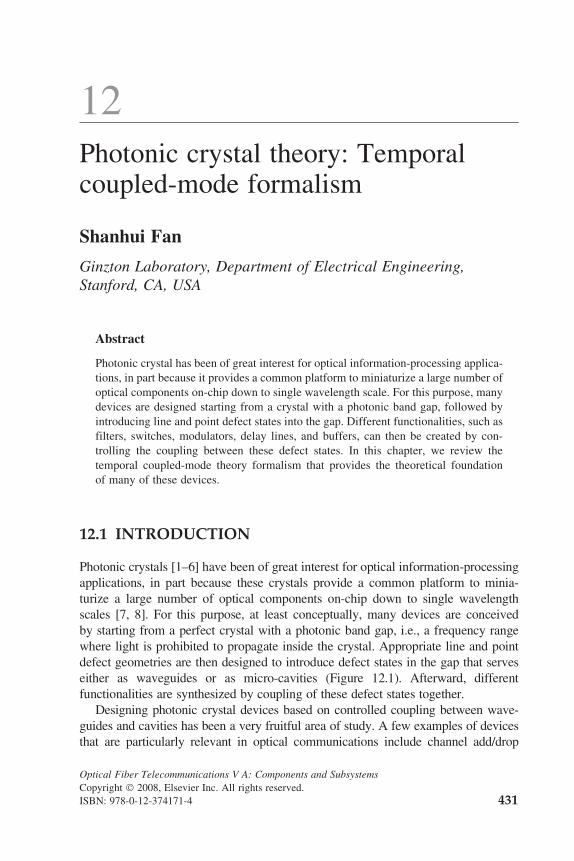
defect geometries are then designed to introduce defect states in the gap that serves
either as waveguides or as micro-cavities (Figure 12.1). Afterward, different
functionalities are synthesized by coupling of these defect states together.
Designing photonic crystal devices based on controlled coupling between wave-
guides and cavities has been a very fruitful area of study. A few examples of devices
that are particularly relevant in optical communications include channel add/drop
Optical Fiber Telecommunications V A: Components and Subsystems
Copyright � 2008, Elsevier Inc. All rights reserved.
ISBN: 978-0-12-374171-4 431
filters [9–17] for wavelength division multiplexing (WDM), optical switches [18–24],
isolators [25–27], static delay lines [28–32], and dynamic optical buffers [33–38].
In this chapter, we review the temporal coupled-mode theory formalism that
provides the theoretical foundation for many of these devices. As examples of
applications of this formalism, we then discuss nonlinear bistable optical switch
and dynamic optical buffers.
12.2 TEMPORAL COUPLED-MODE THEORYFOR OPTICAL RESONATORS
Temporal coupled-mode theory [39] is a powerful theoretical framework for under-
standing a variety of effects that arise from the coupling between waveguides and
resonators. This theory is applicable when the quality factor of the resonator
is sufficiently high, such that the amplitude inside the resonator can be assumed
to decay exponentially in time in the absence of external stimulus. On the basis
of this assumption, a complete theoretical formalism can then be systematically built
up using very general arguments such as energy conservation and time-reversal
symmetry. The beauty of the theory is that aside from a few parameters representing
resonant frequencies and coupling constants, the details of the resonators and the
waveguides are irrelevant. Hence, such a theory is particularly attractive for photo-
nic crystal device structures, which tend to have complicated geometry.
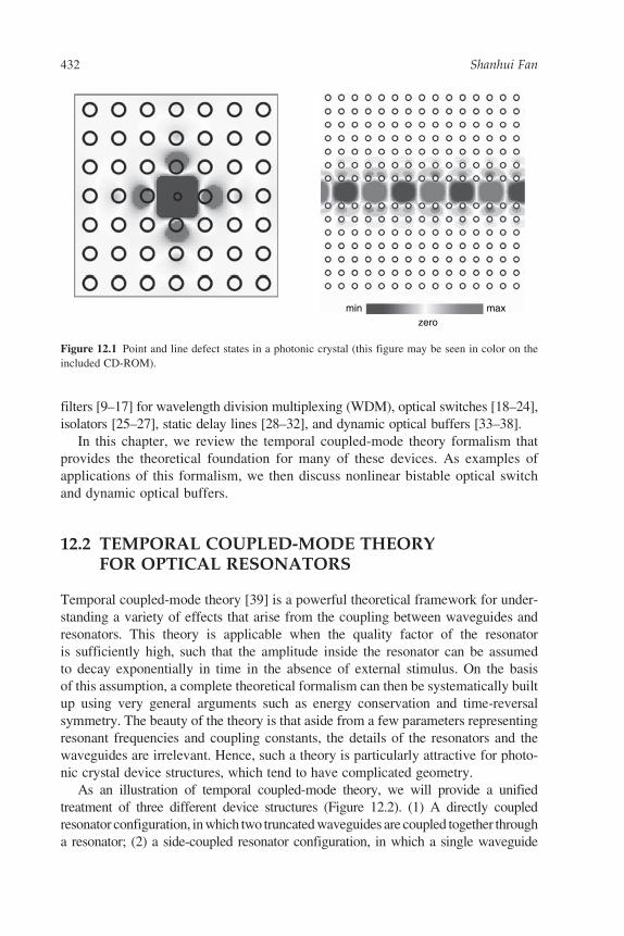
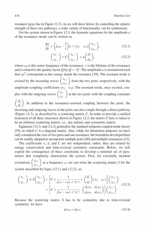
As an illustration of temporal coupled-mode theory, we will provide a unified
treatment of three different device structures (Figure 12.2). (1) A directly coupled
resonator configuration, in which two truncated waveguides are coupled together through
a resonator; (2) a side-coupled resonator configuration, in which a single waveguide
min maxzero
Figure 12.1 Point and line defect states in a photonic crystal (this figure may be seen in color on the
included CD-ROM).
432 Shanhui Fan
is side-coupled to a standing wave resonator; and (3) a Fano-interference configur-
ation, which is similar to (2), except an additional scatterer is placed inside the wave-
guide. These devices provide a number of useful filtering and switching functionalities.
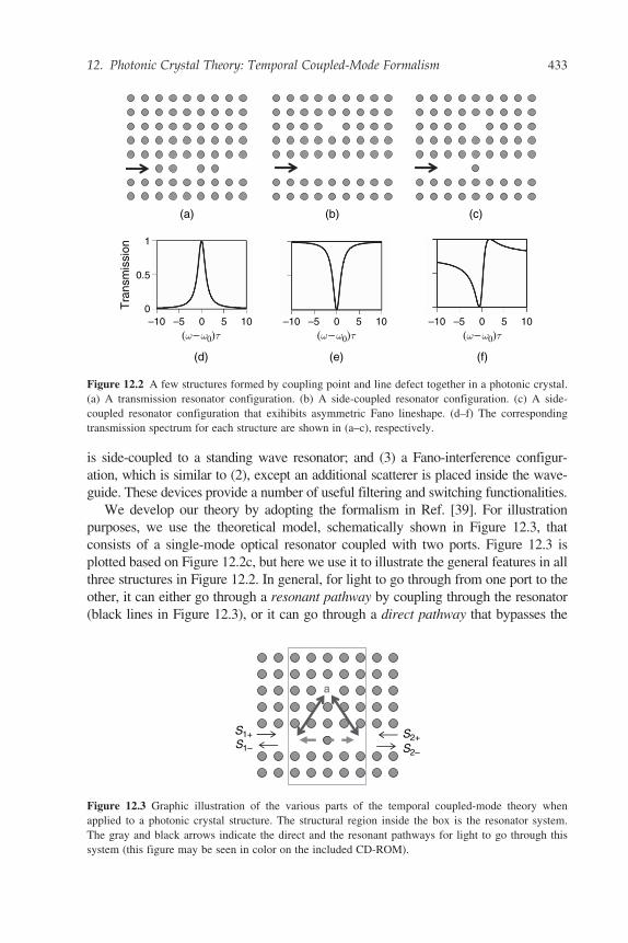
We develop our theory by adopting the formalism in Ref. [39]. For illustration
purposes, we use the theoretical model, schematically shown in Figure 12.3, that
consists of a single-mode optical resonator coupled with two ports. Figure 12.3 is
plotted based on Figure 12.2c, but here we use it to illustrate the general features in all
three structures in Figure 12.2. In general, for light to go through from one port to the
other, it can either go through a resonant pathway by coupling through the resonator
(black lines in Figure 12.3), or it can go through a direct pathway that bypasses the
S1+S1–
S2+S2–
a
Figure 12.3 Graphic illustration of the various parts of the temporal coupled-mode theory when
applied to a photonic crystal structure. The structural region inside the box is the resonator system.
The gray and black arrows indicate the direct and the resonant pathways for light to go through this
system (this figure may be seen in color on the included CD-ROM).
(a) (b) (c)
(d)
1
0.5
0–10 –5 0 5 10 –10 –5 0 5 10 –10 –5 0 5 10
(e) (f)
Tra
nsm
issi
on
(ω − ω0)τ (ω − ω0)τ (ω − ω0)τ
Figure 12.2 A few structures formed by coupling point and line defect together in a photonic crystal.
(a) A transmission resonator configuration. (b) A side-coupled resonator configuration. (c) A side-
coupled resonator configuration that exihibits asymmetric Fano lineshape. (d–f) The corresponding
transmission spectrum for each structure are shown in (a–c), respectively.
12. Photonic Crystal Theory: Temporal Coupled-Mode Formalism 433
resonator (gray line in Figure 12.3). As we will show below, by controlling the relative
strength of these two pathways, a wide variety of functionality can be synthesized.
For the system shown in Figure 12.3, the dynamic equations for the amplitude a
of the resonance mode can be written as
da
dt= j!0 �
1
�
� �aþ �1 �2ð Þ
s1þ
s2þ
� �, (12.1)
s1�
s2�
� �= C
s1þ
s2þ
� �þ a
d1
d2
� �, (12.2)
where !0 is the center frequency of the resonance, � is the lifetime of the resonance
and is related to the quality factor Q by Q= !0�2 . The amplitude a is normalized such
that jaj2 corresponds to the energy inside the resonator [39]. The resonant mode is
excited by the incoming wavess1þs2þ
� �from the two ports, respectively, with the
amplitude-coupling coefficients (�1 �2). The resonant mode, once excited, cou-
ples with the outgoing wavess1�s2�
� �at the two ports with the coupling constants
d1d2
� �. In addition to the resonance-assisted coupling between the ports, the
incoming and outgoing waves in the ports can also couple through a direct pathway
(Figure 12.3), as described by a scattering matrix C. In order to provide a unified
treatment of all three structures shown in Figure 12.2, the matrix C here is taken to
be an arbitrary scattering matrix, i.e., any unitary and symmetric matrix.
Equations (12.1) and (12.2) generalize the standard temporal coupled-mode theory
[39], in which C is a diagonal matrix. Also, while for illustration purposes we have
only considered the case of two ports and one resonance, the formalism developed here
can be readily adopted to incorporate multiple ports [40] and multiple resonances [41].
The coefficients �, d, and C are not independent; rather, they are related by
energy conservation and time-reversal symmetry constraints. Below, we will
exploit the consequence of these constraints to develop a minimal set of para-
meters that completely characterize the system. First, for externally incident
excitationss1þs2þ
� �at a frequency !, we can write the scattering matrix S for the
system described by Eqns (12.1) and (12.2), as:
s1�
s2�
� �� S
s1þ
s2þ
� �= Cþ 1
jð!� !0Þ þ 1=��
d1
d2
� ��1 �2ð Þ
� �s1þ
s2þ
� �
= Cþ 1
jð!� !0Þ þ 1=��
d1�1 d1�2
d2�1 d2�2
� �� �s1þ
s2þ
� � (12.3)
Because the scattering matrix S has to be symmetric due to time-reversal
symmetry, we have
d1�2 = d2�1 (12.4)
434 Shanhui Fan
Also, with incoming wave amplitudess1þs2þ
� �, the amplitude of the resonant
mode is
a =1
j !� !0ð Þ þ 1=��1s1þ þ �2s2þð Þ (12.5)
Instead of considering the case where the resonator is excited by externally
incident wavess1þs2þ
� �, let us now consider an alternative scenario, in which the
external incident wave is absent, i.e.,s1þs2þ
� �= 0, and at t = 0, there is a finite
amplitude of the resonance. At t > 0, the resonant mode shall decay exponentially
into the two ports, as
d aj j2
dt= � 2
�
� �aj j2 = � s1�j j2þ s2�j j2
� �= � aj j2 d1j j2þ d2j j2
� �, (12.6)
which requires that
d1j j2þ d2j j2 = 2=�: (12.7)
Now, let us perform a time-reversal transformation for the exponential decay
process as described by Eqn (12.6). The time-reversed case is represented by
feeding the resonator with exponentially growing waves at a complex frequency
!=!0 � j � 1=� , with incident amplitudes at the two ports when t = 0 equal to
s�1�s�2�
� �. Such excitations cause a resonance amplitude a* at t = 0 to grow expo-
nentially in time. Using Eqn (12.1) at the complex frequency !=!0 � j � 1=� , we
have a�= �2 �1s
�1� þ �2s�2�
� = �
2 �1d�1 þ �2d�2
� a�, and therefore
�1d�1 þ �2d�2 =2
�(12.8)
Combining Eqns (12.4), (12.7) and (12.8), we are led to an important conclusion:
�1 = d1; �2 = d2: (12.9)
The time-reversed excitations�1�s�2�
� �also has to satisfy the condition that no
outgoing wave shall occur upon such excitations, i.e.,
0 = Cs�1�s�2�
� �þ a�
d1
d2
� �= a�C
d1
d2
� ��þ a�
d1
d2
� �: (12.10)
12. Photonic Crystal Theory: Temporal Coupled-Mode Formalism 435
Thus, the coupling constants jdi have to satisfy a further condition:
Cd�1d�2
� �= �
d1
d2
� �: (12.11)
Hence, the coupling constants in general cannot be arbitrary but are instead related
to the scattering matrix of the direct process.
To check that the constraints, Eqns (12.7) and (12.9) and (12.11), indeed
produce a self-consistent temporal coupled-mode theory, we need to ensure that
the scattering matrix S, as defined by Eqn (12.3), is unitary. For this purpose, we
note that
Sþ= Cþ þ 1
�jð!� !0Þ þ 1=��
d1
d2
� ��d1 d2ð Þ� (12.12)
and therefore
SSþ=CCþ þ 2=�ð Þ!�!0ð Þ2þ 1=�ð Þ2
d1
d2
!d�1 d�2ð Þ
þ 1
�j !�!0ð Þþ 1=�ð ÞCd�1
d�2
!d�1 d�2ð Þþ 1
j !�!0ð Þþ 1=�ð Þ
d1
d2
!d1 d2ð ÞCþ (12.13)
Taking advantage of Eqn (12.11) and its complex conjugate,
d1 d2ð ÞCþ= � d1 d2ð Þ�, (12.14)
we can indeed prove the unitary property of the matrix S:
SSþ= CCþþ
2=�
� �!� !0ð Þ2þ 1=�
� �2� 1
�j !� !0ð Þ þ 1=�
� �� 1
j !� !0ð Þ þ 1=�
� �264
375 d1
d2
!d�1 d�2�
= CCþ= I
(12.15)
Below, we apply the general formalism to the structures shown in Figure 12.2.
In general, once the magnitudes of the coupling constants d1 and d2 are fixed, the
phases of the coupling constant can be determined from the scattering matrix C
of the direct process. For the structures shown in Figure 12.2, however, the theory
can be further simplified, because they all possess mirror symmetry. For these
436 Shanhui Fan
structures, if we further assume that the resonance mode is even with respect to the
mirror that maps the two ports, we should have d1 = d2 = d if the reference planes
are symmetrically placed on each side of the mirror plane. With such a symmetric
choice of reference plane location, the scattering matrix for the direct transport
process also acquires a special form [39]:
C = ej�r jt
jt r
� �, (12.16)
where r, t, and � are real constants with r2þ t2 = 1. Using Eqns (12.7) and (12.11),
we can determine d1 and d2 as
d1 = d2 = jej�2
ffiffiffiffiffiffiffiffiffiffiffir þ jt
p�ffiffiffi1
�
r(12.17)
and consequently the scattering matrix S for the overall system as
S = ej�r jt
jt r
� �� 1=�
j !� !0ð Þ þ 1=�r þ jtð Þ
1 1
1 1
� �� �: (12.18)
From Eqn (12.18), the power transmission coefficient T is therefore
T =t2 !� !0ð Þ2þ r2 1=�ð Þ2þ 2rt !� !0ð Þ 1=�ð Þ
!� !0ð Þ2þ 1=�ð Þ2(12.19)
Using Eqn (12.19), we now discuss the three configurations as shown in
Figure 12.2:
(a) Directly coupled resonator configuration (Figure 12.2a). For this structure,
in the absence of the resonator, a photonic crystal region that acts as a tunneling
barrier separates the two waveguides. Therefore r � 1 and t � 0. The power
transmission spectrum
T =1=�ð Þ2
!� !0ð Þ2þ 1=�ð Þ2(12.20)
exhibits a Lorentzian peak (Figure 12.2(d)). Such a configuration therefore func-
tions as a band-pass filter.
(b) Side-coupled resonator configuration (Figure 12.2(b)). For this structure, in
the absence of the resonator, light propagates in the waveguide unperturbed. If one
chooses the reference plane to be exactly where the resonator is, one has
C=0 11 0
� �. Therefore, in Eqn (12.16) one should set r = 0, t = 1, and �= � �
2.
12. Photonic Crystal Theory: Temporal Coupled-Mode Formalism 437
Using Eqn (12.17), we then have d1 = d2 = jffiffi1�
q. Hence, the power transmission
spectrum becomes
T =!� !0ð Þ2
!� !0ð Þ2þ 1=�ð Þ2(12.21)
At resonance, the destructive interference between the direct transmission and the
resonant pathway produces complete reflection (Figure 12.2(e)). The structure
therefore functions as a band-rejection filter.
(c) Fano interference configuration (Figure 12.2(c)). By introducing additional
scatterer inside the waveguide, one can alter the direct pathway such that neither r
nor t is close to zero. In such a case, the transmission spectrum exhibits a sharp
asymmetric Fano lineshape [42], in which the transmission coefficient rapidly
varies from 0 to 100% within a narrow frequency range (Figure 12.2(f)). The
width of such a frequency range can be smaller than 1=� . Consequently, the use
of such sharp asymmetric lineshapes provides an opportunity for enhancing
the sensitivity in sensors and in reducing the power requirements for optical
switches [43].
These examples quoted above highlight the general theory that describes
waveguide–cavity interaction in photonic crystals.
12.3 USING TEMPORAL COUPLED-MODE THEORYTO PREDICT OPTICAL SWITCHING
In addition to its application in linear devices, as outlined above, the temporal
coupled-mode theory can also be used to design nonlinear switching devices.
Optical bistable devices are of great importance for all-optical information-
processing applications [44]. Photonic crystal switches can be constructed by
introducing Kerr nonlinear material into the resonator for all the three structures
shown in Figure 12.2. Compared with conventional devices, the use of photonic
crystal resonator, which possesses high-quality factor and small modal volume,
results in greatly reduced power requirements [18–24].
A judicious choice of waveguide-cavity coupling schemes further allows one to
optimize the device characteristics that are important for practical applications.
For example, in integrated two-port bistable devices, an important consideration is
the contrast ratio in the transmission between the two bistable states. A high
contrast ratio is beneficial for maximum immunity to noise and detection error,
and for fan-out considerations.
Here, as an application of the temporal coupled-mode theory, we compare the
nonlinear behaviors of the structures shown in Figure 12.2a and 12.2b, when a
Kerr nonlinear material is introduced into the cavity region. (The general Fano
interference case corresponding to Figure 12.2(c) is more complicated and can
438 Shanhui Fan
be found in Refs [45–48].) A Kerr nonlinear material has an intensity-dependent
index n = n0 þ n2I. Assuming light is injected into the structure from port 1 only,
i.e., S2þ = 0, from Eqn (12.5), the energy in the cavity therefore in both cases
become
aj j2 =1=�
!� !resð Þ2þ 1=�ð Þ2s1þj j2 (12.22)
(This equation in fact holds true for the general Fano interference case as well.) For
the nonlinear system, the resonant frequency !res becomes dependent upon the
total energy inside the cavity by
!res =!0 � � aj j2 (12.23)
where !0 is the resonant frequency of the linear cavity, and � is a constant that
relates to the Kerr coefficient, n2, and is inversely proportional to the cavity modal
volume V. [19]
For the directly coupled resonator geometry, the transmitted power Ptrans �jS2–j2 is proportional to the energy inside the cavity by Ptrans = 1
� aj j2.
Consequently, Eqn (12.23) can be converted into
Ptrans
Pin� 1
1þ Ptrans=P0 þ �ð Þ2 (12.24)
where �= (! – !0)� is the normalized detuning between the signal frequency with
the resonant frequency of the cavity itself in the low-intensity limit, and P0 = 1��2
defines the scale of the power, because �/ 1/V and � /Q. The power scale is
reduced by a factor Q2/V when a resonator is used. The photonic crystal resonator,
with its high-quality factor and small modal volume therefore provides an impor-
tant opportunity in general for reducing the power requirement in nonlinear optical
devices.
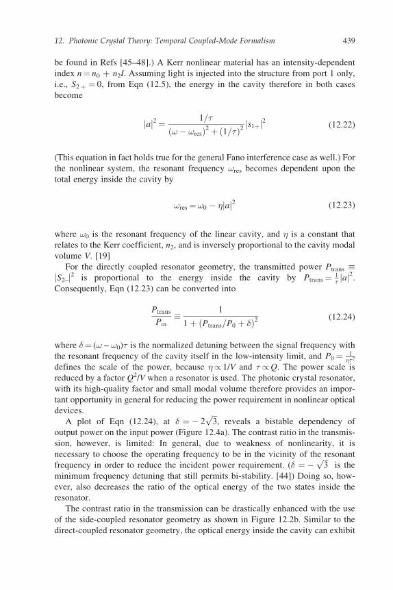
A plot of Eqn (12.24), at � =� 2ffiffiffi3p
, reveals a bistable dependency of
output power on the input power (Figure 12.4a). The contrast ratio in the transmis-
sion, however, is limited: In general, due to weakness of nonlinearity, it is
necessary to choose the operating frequency to be in the vicinity of the resonant
frequency in order to reduce the incident power requirement. (� =�ffiffiffi3p
is the
minimum frequency detuning that still permits bi-stability. [44]) Doing so, how-
ever, also decreases the ratio of the optical energy of the two states inside the
resonator.
The contrast ratio in the transmission can be drastically enhanced with the use
of the side-coupled resonator geometry as shown in Figure 12.2b. Similar to the
direct-coupled resonator geometry, the optical energy inside the cavity can exhibit
12. Photonic Crystal Theory: Temporal Coupled-Mode Formalism 439
bistable dependence on the incident power level and can switch between two states
with either low or high optical energy. However, in this case, one could take
advantage of the interference between the propagating wave inside the waveguide
and the decaying wave from the cavity to greatly enhance achievable contrast ratio
in the transmission between the two bistable states.
Again, starting with Eqs (12.22) and (12.23), but noting in the side-coupled
case, the reflected power Pref � s1�j j2 = 1� aj j2 =Pin � Ptrans, the transmitted
power ratio T for a nonlinear side-coupled resonator can be written as
T � Ptrans
Pin=ðPref=P0 þ �Þ2
1þ ðPref=P0 þ �Þ2(12.25)
For the same frequency detuning �=� 2ffiffiffi3p
, the output power vs input power
for this system is plotted in Figure 12.4b. We note that one of the bistable states
can possess near-zero transmission coefficient, and thus, the contrast ratio can be
infinitely high. This occurs when there is sufficient energy inside the cavity such
that the resonance frequency of the cavity is shifted to coincide with that of the
incident field.
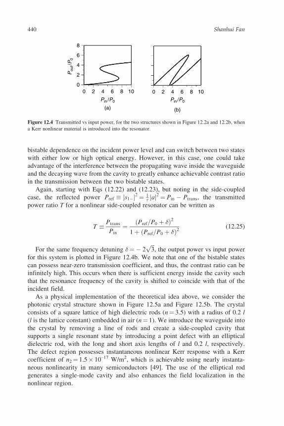
As a physical implementation of the theoretical idea above, we consider the
photonic crystal structure shown in Figure 12.5a and Figure 12.5b. The crystal
consists of a square lattice of high dielectric rods (n = 3.5) with a radius of 0.2 l
(l is the lattice constant) embedded in air (n = 1). We introduce the waveguide into
the crystal by removing a line of rods and create a side-coupled cavity that
supports a single resonant state by introducing a point defect with an elliptical
dielectric rod, with the long and short axis lengths of l and 0.2 l, respectively.
The defect region possesses instantaneous nonlinear Kerr response with a Kerr
coefficient of n2 = 1.5� 10–17 W/m2, which is achievable using nearly instanta-
neous nonlinearity in many semiconductors [49]. The use of the elliptical rod
generates a single-mode cavity and also enhances the field localization in the
nonlinear region.
Pou
t /P
0
Pin /P0 Pin
/P0
(a) (b)
6
6
4
4
2
20
0
8
8 10 6420 8 10
Figure 12.4 Transmitted vs input power, for the two structures shown in Figure 12.2a and 12.2b, when
a Kerr nonlinear material is introduced into the resonator.
440 Shanhui Fan
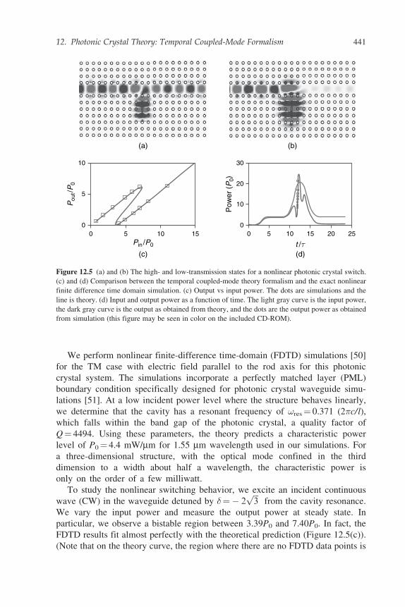
We perform nonlinear finite-difference time-domain (FDTD) simulations [50]
for the TM case with electric field parallel to the rod axis for this photonic
crystal system. The simulations incorporate a perfectly matched layer (PML)
boundary condition specifically designed for photonic crystal waveguide simu-
lations [51]. At a low incident power level where the structure behaves linearly,
we determine that the cavity has a resonant frequency of !res = 0.371 (2�c/l),
which falls within the band gap of the photonic crystal, a quality factor of
Q = 4494. Using these parameters, the theory predicts a characteristic power
level of P0 = 4.4 mW/mm for 1.55 mm wavelength used in our simulations. For
a three-dimensional structure, with the optical mode confined in the third
dimension to a width about half a wavelength, the characteristic power is
only on the order of a few milliwatt.
To study the nonlinear switching behavior, we excite an incident continuous
wave (CW) in the waveguide detuned by �=� 2ffiffiffi3p
from the cavity resonance.
We vary the input power and measure the output power at steady state. In
particular, we observe a bistable region between 3.39P0 and 7.40P0. In fact, the
FDTD results fit almost perfectly with the theoretical prediction (Figure 12.5(c)).
(Note that on the theory curve, the region where there are no FDTD data points is
(a) (b)
(c)
00
5
10
5Pin
/P0
Pou
t /P
0
0
10
20
30
10 15 0 5 10 15 2520
(d)t
/τ
Pow
er (
P0)
Figure 12.5 (a) and (b) The high- and low-transmission states for a nonlinear photonic crystal switch.
(c) and (d) Comparison between the temporal coupled-mode theory formalism and the exact nonlinear
finite difference time domain simulation. (c) Output vs input power. The dots are simulations and the
line is theory. (d) Input and output power as a function of time. The light gray curve is the input power,
the dark gray curve is the output as obtained from theory, and the dots are the output power as obtained
from simulation (this figure may be seen in color on the included CD-ROM).
12. Photonic Crystal Theory: Temporal Coupled-Mode Formalism 441
unstable.) The contrast ratio between the upper and the lower branches approaches
infinity as transmission drops to zero in the lower branch in transmission.
Figure 12.5(a) and 12.5(b) show the field patterns for the two bistable states for
the same input CW power level of 3.95P0. Figure 12.5(a) corresponds to the high
transmission state. In this state, the cavity is off resonance with the excitation. The
field inside the cavity is low and thus the decaying field amplitude from the cavity
is negligible. Figure 12.5b corresponds to the low transmission state. Here, the
field intensity inside the cavity is much higher, pulling the cavity resonance
frequency down to the excitation frequency of the incident field. The decaying
field amplitude from the cavity is significant, and it interferes destructively with
the incoming field. Thus, it is indeed the interference between the wave propagat-
ing in the waveguide and the decaying amplitude from the cavity that result in the
high contrast ratio in transmission.
The FDTD analysis also reveals that the transmission can be switched to the
lower branch from the upper branch with a pulse. Figure 12.5(d) shows the peak
power in each optical period in the waveguide as a function of time, as we switch
the system between the two bistable states shown in Figures 12.5(a) and 12.5(b).
As the input is initially increased to the CW power level of 3.95P0, the system
evolves into a high transmission state, with the transmitted power of 3.65P0.
The switching then occurs after a pulse, which possesses a peak power 20.85P0,
the same carrier frequency as that of CW, and a rise time and a width equal to the
cavity lifetime, is superimposed upon the CW excitation. The pulse pushes
the stored optical energy inside the cavity above the bistable threshold. After the
pulse has passed through the cavity, the system switches to the bistable state with
low transmission power of 0.25P0.
The switching dynamics, as revealed by the FDTD analysis, can also in fact be
completely accounted for with temporal coupled-mode theory developed in this
chapter. The coupled-mode equations (Eqn (12.1)) can be adopted to solve the
reflected amplitude s1� in terms of the input amplitude s1þ as
ds1�dt
= i!0 1� 1
2Q
js1�j2
P0
!s1� �
1
�s1� �
1
�s1þ, (12.26)
from which the transmitted power can then be obtained as js1þ j2 – js21 – j. It is
important to note that the FDTD analysis takes into account the full effects of the
nonlinearity. The coupled-mode theory, on the other hand, neglects higher harmo-
nics of the carrier frequency generated by the nonlinearity. Nevertheless, because
the switching and the cavity decay time scales are far larger than the optical period,
the agreements between the coupled-mode theory and FDTD simulations are
excellent as shown in Figure 12.5(d). Thus, we show that the nonlinear dynamics
in photonic crystal structures can be completely accounted for using coupled-mode
theory, which provides a rigorous and convenient framework for analyzing com-
plex nonlinear processes and devices.
442 Shanhui Fan
12.4 STOPPING LIGHT IN DYNAMIC PHOTONICCRYSTALS
As a last example of this chapter, we show that one could use temporal coupled-
mode theory as a guide for designing dynamic photonic crystals. The idea of
dynamic photonic crystal is to modulate the property of a crystal while an optical
pulse is inside the crystal. In doing so, the spectrum of the pulse can be molded
almost arbitrarily with a small refractive index modulation, leading to highly
nontrivial information-processing capabilities on chip. As examples of such cap-
abilities, we show that the bandwidth of a light pulse can be compressed to zero,
resulting in all-optical stopping and storage of light [33–38].
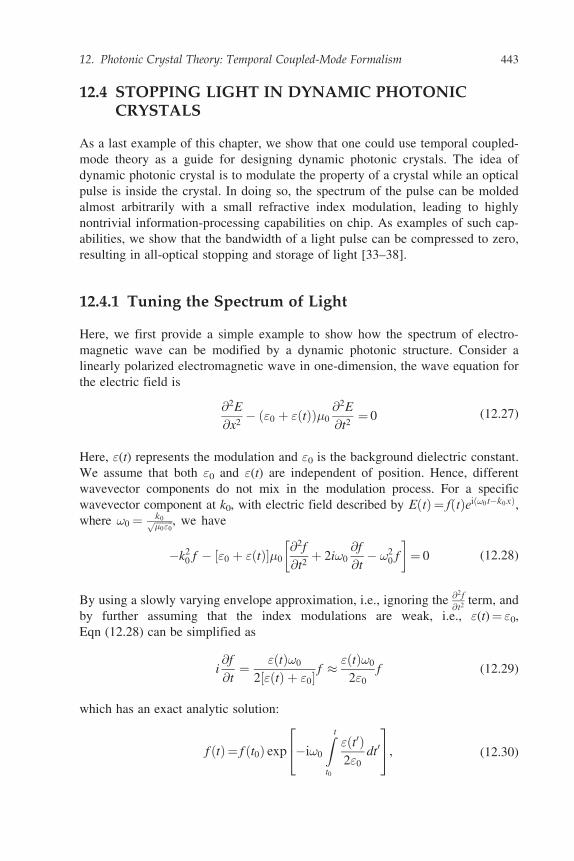
12.4.1 Tuning the Spectrum of Light
Here, we first provide a simple example to show how the spectrum of electro-
magnetic wave can be modified by a dynamic photonic structure. Consider a
linearly polarized electromagnetic wave in one-dimension, the wave equation for
the electric field is
@2E
@x2� "0 þ " tð Þð Þ�0
@2E
@t2= 0 (12.27)
Here, "(t) represents the modulation and "0 is the background dielectric constant.
We assume that both "0 and "(t) are independent of position. Hence, different
wavevector components do not mix in the modulation process. For a specific
wavevector component at k0, with electric field described by E tð Þ= f tð Þei !0t�k0xð Þ,where !0 = k0ffiffiffiffiffiffiffi
�0"0p , we have
�k20 f � "0 þ " tð Þ½ ��0
@2f
@t2þ 2i!0
@f
@t� !2
0 f
� �= 0 (12.28)
By using a slowly varying envelope approximation, i.e., ignoring the @2f
@t2term, and
by further assuming that the index modulations are weak, i.e., "(t) = "0,
Eqn (12.28) can be simplified as
i@f
@t=
" tð Þ!0
2 " tð Þ þ "0½ � f �" tð Þ!0
2"0
f (12.29)
which has an exact analytic solution:
f tð Þ= f t0ð Þ exp �i!0
Z t
t0
" t0ð Þ2"0
dt0
24
35, (12.30)
12. Photonic Crystal Theory: Temporal Coupled-Mode Formalism 443
where t0 is the starting time of the modulation. Thus, the “instantaneous
frequency” of the electric field for this wavevector component is
! tð Þ=!0 1� " tð Þ2"0
� �(12.31)
We note that frequency change is proportional to the magnitude of the refrac-
tive index shift alone. Thus, the process defined here differs in a fundamental way
from traditional nonlinear optical processes. For example, in a conventional sum
frequency conversion process, in order to convert the frequency of light from !1 to
!2, modulations at a frequency !2 – !1 need to be provided. In contrast, in the
process described here, regardless of how slow the modulation is, as long as light is
in the system, the frequency shift can always be accomplished [52]. Below, we will
demonstrate some very spectacular consequence of such frequency shift in the
dynamic photonic crystal, in its application for stopping a light pulse all-optically.
12.4.2 General Conditions for Stopping Light
By stopping light, we aim to reduce the group velocity of a light pulse to zero, while
completely preserving all the coherent information encoded in the pulse. Such
capability holds the key to the ultimate control of light and has profound implica-
tions for optical communications and quantum information processing [53, 54].
There has been extensive work attempting to control the speed of light using
optical resonances in static photonic crystal structures. Group velocities as low as
10–2 c for pulse propagation with negligible distortion have been experimentally
observed in waveguide band edges or with coupled resonator optical waveguides
(CROW) [29, 55–56]. Nevertheless, such structures are fundamentally limited by
the delay-bandwidth product constraint—the group delay from an optical reso-
nance is inversely proportional to the bandwidth within which the delay occurs
[32, 57]. Therefore, for a given optical pulse with a certain temporal duration and
corresponding frequency bandwidth, the minimum group velocity achievable is
limited. In a CROW waveguide structure, for example, the minimum group
velocity that can be accomplished for pulses at 10 Gbit/s rate with a wavelength
of 1.55 mm is no smaller than 10–2 c. For this reason, static photonic structures
could not be used to stop light.
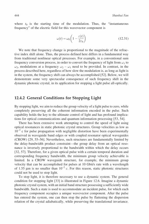
To stop light, it is therefore necessary to use a dynamic system. The general
condition for stopping light [33] is illustrated in Figure 12.6. Imagine a dynamic
photonic crystal system, with an initial band structure possessing a sufficiently wide
bandwidth. Such a state is used to accommodate an incident pulse, for which each
frequency component occupies a unique wavevector component. After the pulse
has entered the system, one can then stop the pulse by flattening the dispersion
relation of the crystal adiabatically, while preserving the translational invariance.
444 Shanhui Fan
In doing so, the spectrum of the pulse is compressed, and its group velocity is
reduced. In the meantime, because the translational symmetry is still preserved, the
wavevector components of the pulse remain unchanged, and thus, one actually
preserves the dimensionality of the phase space. This is crucial in preserving all the
coherent information encoded in the original pulse during the dynamic process.
12.4.3 Tunable Fano Resonance
To create a dynamic photonic crystal, one needs to adjust its properties as a function
of time. This can be accomplished by modulating the refractive index, either with
electro-optic or with nonlinear optic means. However, the amount of refractive
index tuning that can be accomplished with standard optoelectronics technology is
generally quite small, with a fractional change typically on the order of �nn : 10�4.
Therefore, we employ Fano interference schemes in which a small refractive index
modulation leads to a very large change of the bandwidth of the system. The
essence of Fano interference scheme is the presence of multipath interference, in
which at least one of the paths includes a resonant tunneling process [42]. As we
have argued in Section 12.2, such interference can be used to greatly enhance the
sensitivity of resonant devices to small refractive index modulation [43].
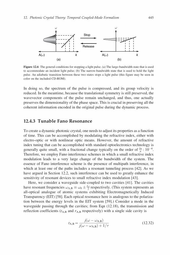
Here, we consider a waveguide side-coupled to two cavities [41]. The cavities
have resonant frequencies !A,B � !0 �!2 respectively. (This system represents an
all-optical analogue of atomic systems exhibiting Electromagnetically Induced
Transparency (EIT) [58]. Each optical resonance here is analogous to the polariza-
tion between the energy levels in the EIT system [59].) Consider a mode in the
waveguide passing through the cavities; from Eqn (12.18), the transmission and
reflection coefficients (tA,B and rA,B respectively) with a single side cavity is
tA,B =j !� !A,Bð Þ
j !� !A,Bð Þ þ 1=�(12.32)
ω
kA(ω) kA(ω)
ω
Stop
Release
(a) (b)
Figure 12.6 The general conditions for stopping a light pulse. (a) The large-bandwidth state that is used
to accommodate an incident light pulse; (b) The narrow-bandwidth state that is used to hold the light
pulse. An adiabatic transition between these two states stops a light pulse (this figure may be seen in
color on the included CD-ROM).
12. Photonic Crystal Theory: Temporal Coupled-Mode Formalism 445
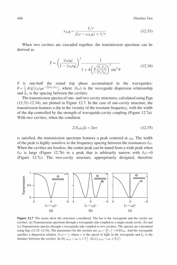
rA,B =1=�
j !� !A,Bð Þ þ 1=�(12.33)
When two cavities are cascaded together, the transmission spectrum can be
derived as
T =tAtBj j
1� rArBj j
� �21
1þ 4
ffiffiffiffiffiffiffiffiffiffiffirArBj j
p1� r
ArBj j
� �2
sin2 (12.34)
is one-half the round trip phase accumulated in the waveguides:
= 12Arg rArBe
�2j !ð ÞL1 �
, where (!) is the waveguide dispersion relationship
and L1 is the spacing between the cavities.
The transmission spectra of one- and two-cavity structures, calculated using Eqn
(12.32–12.34), are plotted in Figure 12.7. In the case of one-cavity structure, the
transmission features a dip in the vicinity of the resonant frequency, with the width
of the dip controlled by the strength of waveguide-cavity coupling (Figure 12.7a).
With two cavities, when the condition
2 !0ð ÞL = 2n� (12.35)
is satisfied, the transmission spectrum features a peak centered at !0. The width
of the peak is highly sensitive to the frequency spacing between the resonances �!.
When the cavities are lossless, the center peak can be tuned from a wide peak when
�! is large (Figure 12.7b) to a peak that is arbitrarily narrow with �!!0
(Figure 12.7c). The two-cavity structure, appropriately designed, therefore
50
Tran
smis
sion
0.5
1
(a) (b) (c)
0 –5(ω – ω0)τ
5 0 –5(ω – ω0)τ
5 0 –5(ω – ω0)τ
Figure 12.7 The insets show the structures considered. The bar is the waveguide and the circles are
cavities. (a) Transmissions spectrum through a waveguide side-coupled to a single-mode cavity. (b) and
(c) Transmission spectra through a waveguide side coupled to two cavities. The spectra are calculated
using Eqs (12.32–12.34), The parameters for the cavities are !0 = 2�cL1
, 1� = 0:05!0. And the waveguide
satisfies a dispersion relation !ð Þ= !c, where c is the speed of light in the waveguide and L1 is the
distance between the cavities. In (b) !a,b =!0 1:5 1� : In ðcÞ!a,b =!0 0:2 1
�.
446 Shanhui Fan
behaves as a tunable bandwidth filter (as well as a tunable delay element), in which
the bandwidth can be in principle adjusted by any order of magnitude with very
small refractive index modulation.
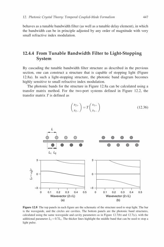
12.4.4 From Tunable Bandwidth Filter to Light-StoppingSystem
By cascading the tunable bandwidth filter structure as described in the previous
section, one can construct a structure that is capable of stopping light (Figure
12.8a). In such a light-stopping structure, the photonic band diagram becomes
highly sensitive to small refractive index modulation.
The photonic bands for the structure in Figure 12.8a can be calculated using a
transfer matrix method. For the two-port systems defined in Figure 12.2, the
transfer matrix T is defined as
s2þ
s2�
� �= T
s1þ
s1�
� �(12.36)
0
–3
0
3
(a)
L1 L2
L
(b)
0.1 0.2
Wavevector (2π/L)0.3 0.4 0.5
(ω –
ω0)
τ
0
–3
0
3
0.1 0.2
Wavevector (2π/L)0.3 0.4 0.5
Figure 12.8 The top panels in each figure are the schematic of the structure used to stop light. The bar
is the waveguide, and the circles are cavities. The bottom panels are the photonic band structures,
calculated using the same waveguide and cavity parameters as in Figure 12.7(b) and 12.7(c), with the
additional parameter L2 = 0.7L1. The thicker lines highlight the middle band that can be used to stop a
light pulse.
12. Photonic Crystal Theory: Temporal Coupled-Mode Formalism 447
For a waveguide side coupled to a single resonator with resonance frequency !i
can be calculated from the scattering matrix S (Eqn (12.3)) as [60]:
Tci=
1þ j=ð!� !iÞ� j=ð!� !iÞ��j=ð!� !iÞ� 1� j=ð!� !iÞ�
� �(12.37)
The transfer matrix through an entire unit cell in Figure 12.8 can then be deter-
mined as
T = Tc1Tl1 Tc2
Tl2 , (12.38)
where Tli =e�jLi 00 ejLi
� �is the transmission matrix for a waveguide section of
length Li. Here, is the wavevector of the waveguide at a given frequency !.
Because det(T) = 1, the eigenvalues of T can be represented as eikl, e–ikl, where
L = L1þ L2 is the length of the unit cell, and k (when it is real) corresponds to the
Bloch wavevector of the entire system. Therefore, we obtain the band diagram of
the system as [35]
1
2Tr Tð Þ= cosðkLÞ= f !ð Þ � cosðLÞ þ Cþ
ð!� !AÞþ C�ð!� !BÞ
, (12.39)
where C= 1� sinðLÞ
2 sinðL1Þ sinðL2Þð!A�!BÞ�2 . In the frequency range where j f(!)j< 1,
the system supports propagating modes, while j f(!)j > 1 corresponds to the fre-
quency ranges of the photonic band gaps.
The band diagrams thus calculated are shown in Figure 12.8, in which the
waveguide and cavity parameters are the same as those used to generate the
transmission spectrum in Figure 12.7. In the vicinity of the resonances, the system
supports three photonic bands, with two gaps occurring around !A and !B. The
width of the middle band depends strongly on the resonant frequencies !A, !B. By
modulating the frequency spacing between the cavities, one goes from a system
with a large bandwidth (Figure 12.8(a)) to a system with a very narrow bandwidth
(Figure 12.8b). In fact, it can be analytically proved that the system can support a
band that is completely flat in the entire first Brillouin zone [35], allowing a light
pulse to be frozen inside the structure with the group velocity reduced to zero.
Moreover, the gaps surrounding the middle band have sizes on the order of the
cavity-waveguide coupling rate, 1/� , and are approximately independent of the
slope of the middle band. Thus, by increasing the waveguide-cavity coupling rate,
this gap can be made large, which is important for preserving the coherent
information during the dynamic bandwidth compression process [33].
12.4.5 Numerical Demonstration in a Photonic Crystal
The system presented above can be implemented in a photonic crystal of a square
lattice of dielectric rods (n = 3.5) with a radius of 0.2a (a is the lattice constant)
448 Shanhui Fan
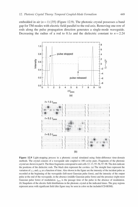
embedded in air (n = 1) [35] (Figure 12.9). The photonic crystal possesses a band
gap for TM modes with electric field parallel to the rod axis. Removing one row of
rods along the pulse propagation direction generates a single-mode waveguide.
Decreasing the radius of a rod to 0.1a and the dielectric constant to n = 2.24
1.0
0.8
0.6
0.4
0.2
0.00 1 2 3 4 5 6 7 8 9 10
–8
–6
–4
–2
0
2
4
6
8
(a)
pulse stopped
pulse released
t /t pass
(b)
t = 1.0 t pass
t = 5.2 t pass
t = 6.3 t pass
Inte
nsity
(ω –
ω0)
τ
Figure 12.9 Light-stopping process in a photonic crystal simulated using finite-difference time-domain
methods. The crystal consists of a waveguide side coupled to 100 cavity pairs. Fragments of the photonic
crystal are shown in part b. The three fragments correspond to unit cells 12–13, 55–56, 97–98. The dots indicate
the positions of the dielectric rods. The black dots represent the cavities. (a) The straight lines represent the
variation of !A and !B as a function of time. Also shown in the figure are the intensity of the incident pulse as
recorded at the beginning of the waveguide (left-most Gaussian pulse form), and the intensity of the output
pulse at the end of the waveguide, in the absence (middle Gaussian pulse form) and the presence (right-most
Gaussian pulse form) of modulation. tpass is the passage time of the pulse in the absence of modulation.
(b) Snapshots of the electric field distributions in the photonic crystal at the indicated times. The gray regions
represent areas with significant field (this figure may be seen in color on the included CD-ROM).
12. Photonic Crystal Theory: Temporal Coupled-Mode Formalism 449
provides a single-mode cavity with resonance frequency at !c = 0.357� (2�c/a).
The nearest neighbor cavities are separated by a distance of l1 = 2a along the
propagation direction, and the unit cell periodicity is l = 8a. The waveguide-cavity
coupling occurs through barrier of one rod, with a coupling rate of 1� =!c=235:8.
The resonant frequencies of the cavities are tuned by refractive index modulation
of the cavity rods.
We simulate the entire process of stopping light for N = 100 pairs of cavities
with FDTD method, which solves Maxwell’s equations without approximation.
The dynamic process for stopping light is shown in Figure 12.9. We generate a
Gaussian pulse in the waveguide (The process is independent of the pulse shape).
The excitation reaches its peak at t = 0.8tpass, where tpass is the traversal time of the
pulse through the static structure. During the pulse generation, the cavities have a
large frequency separation. The field is concentrated in both the waveguide and the
cavities (Figure 12.9b, t = 1.0tpass), and the pulse propagates at a relatively high
speed of vg = 0.082 c. After the pulse is generated, we gradually reduce the
frequency separation of the two cavities. During this process, the speed of light
is drastically reduced to zero. As the bandwidth of the pulse is reduced, the field
concentrates in the cavities (Figure 12.9b, t = 5.2tpass). When zero group velocity
is reached, the photon pulse can be kept in the system as a stationary waveform for
any time duration. In this simulation, we store the pulse for a time delay of 5.0tpass,
and then release the pulse by repeating the same index modulation in reverse
(Figure 12.9(b), t = 6.3tpass). The pulse intensity as a function of time at the right
end of the waveguide is plotted in Figure 12.9a, and shows the same temporal
shape as both the pulse that propagates through the unmodulated system and the
initial pulse recorded at the left end of the waveguide. Thus, the pulse is perfectly
recovered without distortion after the intended delay.
12.4.6 Future Prospects of Dynamic Photonic CrystalSystem
In the all-optical light-stopping scheme presented above, for a small refractive
index shift of �n/n = 10–4 achievable in practical optoelectronic devices, and
assuming a carrier frequency of approximately 200 THz, as used in optical com-
munications, the achievable bandwidths are on the order of 20 GHz, which is
comparable to the bandwidth of a single-wavelength channel in high-speed optical
systems. The storage times are limited only by the cavity lifetimes, which may
eventually approach millisecond time scales as limited by residual loss in trans-
parent materials. The loss in optical resonator systems might be further counter-
acted with the use of gain media in the cavities, or with external amplification.
With such performance, the capabilities for on-chip stopping light should have
important implications for optical communication systems. As an important step
toward its eventual experimental demonstration, the required EIT-like two-cavity
interference effects have recently been observed in a micro-ring cavity system on a
450 Shanhui Fan
silicon chip [61]. The general concept of introducing dynamics into photonic
crystal systems could also be very promising for creating new optical signal-
processing functionalities far beyond the capabilities of static systems.
12.5 CONCLUDING REMARKS
In this chapter, we provide a brief review of the basis of the temporal coupled-mode
theory, as well as its applications in nonlinear and dynamic photonic crystals,
drawing examples from our own recent work in this area. These developments
highlight two general trends in the theoretical work in this field. On one hand, using
computational electromagnetic techniques such as the FDTD methods [50] in
combination with modern large-scale computing architectures, almost any complex
optical processes in photonic crystal can now be simulated through exact numerical
solutions of Maxwell’s equations. On the other hand, with the band structures and
modal properties of passive dielectric photonic structures largely mapped out, one
can now create analytic models with only a few dynamic variables based on these
modal properties, in order to describe the essential physics of optical processes in
photonic crystals. These developments in both theory and simulations, in the context
of very rapid progress in experimental fabrications of photonic crystals, are leading
to ways of controlling light that are truly unprecedented.
ACKNOWLEDGMENT
This work is supported in part by NSF and DARPA. The author acknowledges
Professor Mehmet Fatih Yanik, Professor Marin Soljacic, Professor John
Joannopoulos, Dr Wonjoo Suh, Dr Zheng Wang, Dr Michelle Povinelli, and Sunil
Sandhu for contributions to all aspects of this work.
REFERENCES
[1] E. Yablonovitch, “Inhibited spontaneous emission in solid state physics and electronics,” Phys.
Rev. Lett., 58, 2059–2062, 1987.
[2] S. John, “Strong localization of photons in certain disordered dielectric superlattices,” Phys. Rev.
Lett., 58, 2486–2489, 1987.
[3] J. D. Joannopoulos, R. D. Meade, and J. N. Winn, Photonic Crystals: Molding the Flow of Light,
Princeton University Press, Princeton, NJ, 1995.
[4] C. Soukoulis, ed., Photonic Crystals and Light Localization in the 21st Century, The Netherlands,
NATO ASI Series, Kluwer Academic Publisher, 2001.
[5] S. G. Johnson and J. D. Joannopoulos, Photonic Crystals: The Road from Theory to Practice,
Kluwer Academic Publisher, Boston, 2002.
[6] K. Inoue and K. Ohtaka, Photonic Cryst., Berlin, Springer-Verlag, 2004.
[7] J. D. Joannopoulos, P. R. Villeneuve, and S. Fan, “Photonic crystals: Putting a new twist on light,”
Nature, 386, 143–147, 1997.
12. Photonic Crystal Theory: Temporal Coupled-Mode Formalism 451
[8] A. Mekis, J. C. Chen, I. Kurland et al., “High transmission through sharp bends in photonic crystal
waveguides,” Phys. Rev. Lett., 77, 3787–3790, 1996.
[9] S. Fan, P. R. Villeneuve, J. D. Joannopoulos, and H. A. Haus, “Channel drop tunneling through
localized states,” Phys. Rev. Lett., 80, 960–963, 1998.
[10] S. Fan, P. R. Villeneuve, J. D. Joannopoulos, and H. A. Haus, “Channel drop filters in a photonic
crystal,” Opt. Express., 3, 4–11, 1998.
[11] C. Manolatou, M. J. Khan, S. Fan et al., “Coupling of modes analysis of resonant channel add-drop
filters,” IEEE J. Quant. Electron., 35, 1322–1331, 1999.
[12] S. Noda, A. Chutinan, and M. Imada, “Trapping and emission of photons by a single defect in a
photonic band gap structures,” Nature, 407, 608–610, 2000.
[13] C. Jin, S. Fan, S. Han, and D. Zhang, “Reflectionless multi-channel wavelength demultiplexer in a
transmission resonator configuration,” IEEE J. Quant. Electron., 39, 160–165, 2003.
[14] Y. Akahane, T. Asano, B.-S. Song, and S. Noda, “Investigation of high-Q channel drop filters
using donor-type defects in two-dimensional photonic crystal slabs,” Appl. Phys. Lett., 83,
1513–1515, 2003.
[15] K. H. Hwang and G. H. Song, “Design of a high-Q channel add/drop multiplexer based on the two-
dimensional photonic crystal membrane structure,” Opt. Express., 13, 1948–1957, 2005.
[16] Z. Zhang and M. Qiu, “Coupled-mode analysis of a resonant channel drop filter using waveguides
with mirror boundaries,” J. Opt. Soc. Am. B., 23, 104–113, 2006.
[17] A. Shinya, S. Mitsugi, E. Kuramochi, and M. Notomi, “Ultrasmall multi-port channel drop filter in
two-dimensional photonic crystal on silicon-on-insulator substrate,” Opt. Express., 14, 12394–
12400, 2006.
[18] S. F. Mingaleev and Y. S. Kivshar, “Nonlinear transmission and light localization in photonic-
crystal waveguides,” J. Opt. Soc. Am. B, 19, 2241–2249, 2002.
[19] M. Soljacic, M. Ibanescu, S. G. Johnson et al., “Optimal bistable switching in nonlinear photonic
crystals,” Phys. Rev. E, 66, 055601(R), 2002.
[20] M. Soljacic, C. Luo, J. D. Joannopoulos, and S. Fan, “Nonlinear photonic microdevices for optical
integrations,” Opt. Lett., 28, 637–639, 2003.
[21] M. F. Yanik, S. Fan, and M. Soljacic, “High-contrast all-optical bistable switching in photonic
crystal microcavities,” Appl. Phys. Lett., 83, 2741–3, 2003.
[22] M. F. Yanik, S. Fan, M. Soljacic, and J. D. Joannopoulos, “All-optical transistor action with bistable
switching in photonic crystal cross-waveguide geometry,” Opt. Lett., 28, 2506–2508, 2003.
[23] M. Notomi, A. Shinya, S. Mitsugi et al., “Optical bistable switching action of Si high-Q photonic
crystal nanocavities,” Opt. Express., 13, 2678–2687, 2005.
[24] Y. Tanaka, H. Kawashima, N. Ikeda et al., “Optical bistable operations in AlGaAs-based photonic
crystal slab microcavity at telecommunication wavelengths,” IEEE Photon. Technol. Lett., 18,
1996–1998, 2006.
[25] Z. Wang and S. Fan, “Magneto-optical defects in two-dimensional photonic crystals,” Appl. Phys.
B, 81, 369–375, 2005.
[26] Z. Wang and S. Fan, “Optical circulators in two-dimensional magneto-optical photonic crystals,”
Opt. Lett., 30, 1989–1991, 2005.
[27] Z. Wang and S. Fan, “Add-drop filter in two-dimensional magneto-optical photonic crystals and
suppression of disorder effects by time-reversal breaking,” Photonics and Nanostructures: Funda-
mentals and Applications, 18, 1996–1998, 2006.
[28] N. Stefanou and A. Modinos, “Impurity bands in photonic insulators,” Phys. Rev. B, 57,
12127–12133, 1998.
[29] A. Yariv, Y. Xu, R. K. Lee, and A. Scherer, “Coupled-resonator optical waveguide: a proposal and
analysis,” Opt. Lett., 24, 711–713, 1999.
[30] M. Bayindir, B. Temelkuran, and E. Ozbay, “Tight-binding description of the coupled defect
modes in three-dimensional photonic crystals,” Phys.l Rev. Lett., 84, 2140–2143, 2000.
[31] Y. Xu, Y. Li, R. K. Lee, and A. Yariv, “Scattering-theory analysis of waveguide resonator
coupling,” Phys. Rev. E, 62, 7389–7404, 2000.
452 Shanhui Fan
[32] Z. Wang and S. Fan, “Compact all-pass filters in photonic crystals as the building block for high
capacity optical delay lines,” Phys. Rev. E, 68, Art. No. 066616, 2003.
[33] M. F. Yanik and S. Fan, “Stopping light all-optically,” Phys. Rev. Lett., 92, Art. No. 083901, 2004.
[34] M. F. Yanik and S. Fan, “Time-reversal of light with linear optics and modulators,” Phys. Rev.
Lett., 93, Art. No. 173903, 2004.
[35] M. F. Yanik, W. Suh, Z. Wang, and S. Fan, “Stopping light in a waveguide with an all-optical
analogue of electromagnetically induced transparency,” Phys. Rev. Lett., 93, Art. No. 233903,
2004.
[36] M. F. Yanik and S. Fan, “Stopping and storing light coherently,” Phys. Rev. A, 71, Art.
No. 013803, 2005.
[37] M. F. Yanik and S. Fan, “Dynamic photonic structures: Stopping, storage, and time-reversal of
light,” Studies in Applied Mathematics, 115, 233–254, 2005.
[38] S. Sandhu, M. L. Povinelli, M. F. Yanik, and S. Fan, “Dynamically-tuned coupled resonator delay
lines can be nearly dispersion free,” Opt. Lett., 31, 1981–1983, 2006.
[39] H. A. Haus, Waves and Fields in Optoelectronics, New Jersey, Englewood Cliffs: Prentice-Hall,
1984.
[40] S. Fan, W. Suh, and J. D. Joannopoulos, “Temporal coupled mode theory for Fano resonances in
optical resonators,” J. Opt. Soc. Am. A, 20, 569–573, 2003.
[41] W. Suh, Z. Wang, and S. Fan, “Temporal coupled-mode theory and the presence of non-
orthogonal modes in lossless multimode cavities,” IEEE J. Quant. Electron., 40, 1511–1518,
2004.
[42] U. Fano, “Effects of configuration interaction on intensities and phase shifts,” Phys. Rev., 124,
1866–1878, 1961.
[43] S. Fan, “Sharp asymmetric lineshapes in side-coupled waveguide-cavity systems,” Appl. Phys.
Lett., 80, 908–910, 2002.
[44] H. M. Gibbs, Optical Bistability: Controlling Light with Light, Orlando, Academic Press, 1985.
[45] A. R. Cowan and J. F. Young, “Optical bistability involving photonic crystal microcavities and
Fano lineshapes,” Phys. Rev. E., 68, Art. No. 046606, 2003.
[46] V. Lousse and J. P. Vigeron, “Use of Fano resonances for bistable optical transfer through
photonic crystal films,” Phys. Rev. B., 69, Art. No. 155106, 2004.
[47] A. E. Miroshnichenko and Y. S. Kivshar, “Engineering Fano resonance in discrete arrays,” Phys.
Rev. E., 72, Art. No. 056611, 2005.
[48] S. F. Mingaleev, A. E. Miroshnichenko, Y. S. Kivshar, and K. Busch, “All-optical switching,
bistability, and slow-light transmission in photonic crystal waveguide-resonator systems,” Phys.
Rev. E., 74, Art. No. 046603, 2006.
[49] M. Sheik-Bahae, D. C. Hutchings, D. J. Hagan, and E. W. Van Stryland, “Dispersion of bound
electronic nonlinear refraction in solids,” IEEE J. Quant. Electron., 27, 1296–1309, 1991.
[50] A. Taflove and S. C. Hagness, “Computational Electrodynamics, Norwood MA, Artech House,
2000.
[51] M. Koshiba and Y. Tsuji, “High-performance absorbing boundary conditions for photonic crystal
waveguide simulations,” IEEE Microwave and Wireless Compon. Lett., 11, 152–154, 2001.
[52] E. J. Reed, M. Soljacic, and J. D. Joannopoulos, “Color of shock waves in photonic crystals,”
Phys. Rev. Lett., 91, Art. No. 133901, 2003.
[53] C. Liu, Z. Dutton, C. H. Behroozi, and L. V. Hau, “Observation of coherent optical information
storage in an atomic medium using halted light pulses,” Nature, 409, 490–493, 2001.
[54] D. F. Phillips, A. Fleischhauer, A. Mair et al., “Storage of light in atomic vapors,” Phys. Rev. Lett.,
86, 783–786, 2001.
[55] M. Notomi, K. Yamada, A. Shinya et al., “Extremely large group-velocity dispersion of line-defect
waveguides in photonic crystal slabs,” Phys. Rev. Lett., 87, Art. No. 253902, 2001.
[56] Y. A. Vlasov, M. O’Boyle, H. F. Harmann, and S. J. McNab, “Active control of slow light on a
chip with photonic crystal waveguides,” Nature, 438, 65–69, 2005.
12. Photonic Crystal Theory: Temporal Coupled-Mode Formalism 453
[57] G. Lenz, B. J. Eggleton, C. K. Madsen, and R. E. Slusher, “Optical delay lines based on optical
filters,” IEEE J. Quant. Electron., 37, 525–532, 2001.
[58] S. E. Harris, “Electromagnetically induced transparency,” Phys. Today., 50, 36–42, 1997.
[59] L. Maleki, A. B. Matsko, A. A. Savchenkov, and V. S. Ilchenko, “Tunable delay line with
interacting whispering-gallery-mode resonators,” Opt. Lett., 29, 626–628, 2004.
[60] S. Fan, P. R. Villeneuve, J. D. Joannopoulos et al., “Theoretical investigation of channel drop
tunneling processes,” Phys. Rev. B., 59, 15882–15892, 1999.
[61] Q. Xu, S. Sandhu, M. L. Povinelli et al., “Experimental realization of an on-chip all-optical
analogue to electromagnetically induced transparency,” Phys. Rev. Lett., 96, Art. No. 123901,
2006.
454 Shanhui Fan
13Photonic crystal technologies:Experiment
Susumu Noda
Department of Electronic Science and Engineering,Kyoto University, Kyoto, Japan
Abstract
Photonic crystals, in which the refractive index changes periodically, provide an
exciting new tool for the manipulation of photons and have received keen interest
from a variety of fields. This manuscripts review the recent progresses and future
prospects of photonic crystals and their applications to photonic nanostructure devices.
13.1 INTRODUCTION
Photonic crystals are a kind of nanostructures for light, the refractive indices of
which change in a periodic fashion. They are characterized by the formation of
band structures with respect to photon energy [1, 2] from the analogy to those with
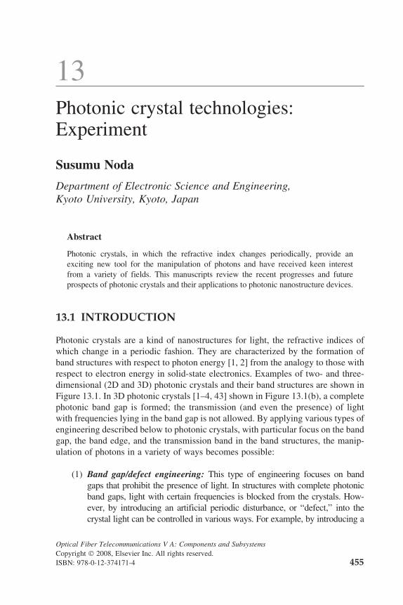
respect to electron energy in solid-state electronics. Examples of two- and three-
dimensional (2D and 3D) photonic crystals and their band structures are shown in
Figure 13.1. In 3D photonic crystals [1–4, 43] shown in Figure 13.1(b), a complete
photonic band gap is formed; the transmission (and even the presence) of light
with frequencies lying in the band gap is not allowed. By applying various types of
engineering described below to photonic crystals, with particular focus on the band
gap, the band edge, and the transmission band in the band structures, the manip-
ulation of photons in a variety of ways becomes possible:
(1) Band gap/defect engineering: This type of engineering focuses on band
gaps that prohibit the presence of light. In structures with complete photonic
band gaps, light with certain frequencies is blocked from the crystals. How-
ever, by introducing an artificial periodic disturbance, or “defect,” into the
crystal light can be controlled in various ways. For example, by introducing a
Optical Fiber Telecommunications V A: Components and Subsystems
Copyright � 2008, Elsevier Inc. All rights reserved.
ISBN: 978-0-12-374171-4 455
line-shaped defect, it is possible to form an ultrasmall waveguide that permits
the transmission of light only along the defect. Light can be trapped at certain
points by introducing point defects, thereby forming photonic nanocavities.
By combining these line and point defects, it is possible to form ultrasmall
photonic circuits (or chips) with various functions. Furthermore, the band
gap itself makes it possible to suppress spontaneous emission, which is a
fundamental factor limiting the performance of various photonic devices.
(2) Band edge engineering: This type of engineering focuses on the band edge, where
the group velocity of light becomes zero. At the band edge, light being propagating
in various directions is combined by Bragg reflection to form a standing wave. By
using this standing wave as a cavity mode, for example, a laser that enables
coherent oscillation over a large 2D area can be realized. The creation of various
types of novel nonlinear optical phenomena might also be possible.
(3) Band engineering: This type of engineering focuses on the transmission
bands that allow the propagation of light. Various types of light control
become possible when the unique dispersion relation obtained from the
band structure can be manipulated. It is anticipated that by considerably
slowing the propagation speed and by altering the propagation direction of
the light in a photonic crystal, or by making negative refraction possible, a
variety of novel applications and photonic devices will be developed.
In addition to the various types of engineering described above, the recent introduc-
tion of a concept of “photonic heterostructures” accelerates the progresses of the field
of photonic crystals. On the basis of the engineering described above, we would like
to introduce some recent developments concerning 2D and 3D photonic crystals.
13.2 BAND GAP/DEFECT ENGINEERING
13.2.1 Two-Dimensional Photonic Crystal Slabs
Two-dimensional photonic crystal research initially targeted structures with
periodicity in two dimensions and a third dimension assumed to be of infinite length
[5], but recently the focus of research has been slab structures [2, 6, 7], such as the one
(a) (b)
Figure 13.1 Schematic representations of (a) a 2D photonic crystal and (b) a 3D photonic crystal.
456 Susumu Noda
shown in Figure 13.1(a), that have a thickness of the order of the wavelength of the
light. The photonic crystal in this figure has a triangular lattice structure. The slab
material is assumed to be a high refractive index medium, such as Si and III–V
semiconductors, and the lattice points are assumed to be comprising a low refractive
index medium, such as air. In 2D photonic crystal slabs, the confinement of light occurs
in the in-plane direction due to a photonic band gap effect, and light is confined in the
perpendicular direction by total internal reflection due to a difference in refractive
indices. Pseudo-3D light control becomes possible as a result. It is, of course, important
to optimize the structure so that leakage of light in the direction perpendicular to the
slab is minimized. Recently, as described below, 2D photonic crystal slabs have been
subjected to various types of band gap/defect engineering, and research with the aim of
realizing ultrasmall photonic circuits has been advancing steadily.
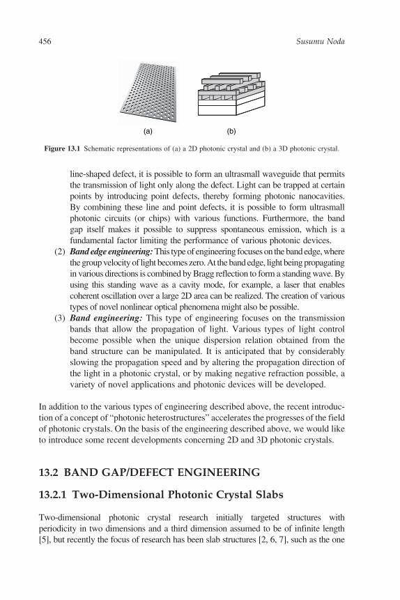
Control of Light by Combined Line/Point-Defect Systems
As shown in Figure 13.2(a), when a line defect is introduced into a 2D photonic
crystal slab, it will act as an ultrasmall optical waveguide. To operate the waveguide
efficiently, it is necessary to devise a way in which the leakage of light in the direction
perpendicular to the slab can be nullified. In 1999, an optical waveguide experiment
was reported [8], but the perpendicular leakage of light was not taken into considera-
tion and the propagation loss was hence extremely large, exceeding 70 dB/mm. A year
later in 2000, detailed results of an examination of the effects of the slab thickness and
the ratio of the low refractive index [the medium (air) that forms the lattice points] to
the high refractive index (the slab material) were reported, and a theoretical zero-loss
waveguide structure was proposed for the first time [9]. In 2001, based on these design
guidelines, a new waveguide experiment was conducted in which a low propagation
loss of 7 dB/mm was obtained [10]. At the same time, discussions were taking place
regarding the effect of modification of the waveguide width on various waveguide
characteristics. It was also pointed out that an increase in propagation loss was caused
by vertical asymmetry in the slab [11]. Regarding this, the importance of using
crystals with a 2D in-plane full band gap was pointed out [12]. Recently, an extremely
(a) (b)
Linedefect
Pointdefect
Figure 13.2 Schematic representations of (a) a line-defect waveguide introduced into a 2D photonic
crystal slab and (b) a combined point-defect resonator and line-defect waveguide system.
13. Photonic Crystal Technologies: Experiment 457
low waveguide loss less than 0.7 dB/mm, one-tenth of the previous best value, has
been achieved [13–15], and it should be possible to fabricate waveguides with
propagation losses of less than 1 dB/cm in the near future. In view of the merits of
the miniaturization enabled by the use of photonic crystals, these recent developments
show that the minimization of waveguide loss in 2D crystal slabs has advanced to the
point where it can almost be ignored.
In conjunction with studies of straight-line waveguides, detailed investigations on
waveguide bends have also been carried out. It was initially pointed out that the
bending of a waveguide was possible in purely 2D crystals, in regions of very broad-
wavelength transmission [5, 16], but that, in slab structures, the effect of light scattering
to the outside of the slab meant that the low-loss band region in the bend part of the
waveguide could not be enlarged to a great extent [9]. Thereafter, the importance of
controlling lattice point shapes positioned in the curved part was highlighted [17], and
the enlargement and shifting of the band area in the curved region were then reported
[18, 19]. In 2004, it was also shown that low-loss curvature of a waveguide at a very
broadband area might be possible even for a bend of 120� [20]. In addition, there have
been some studies of low-loss connections between line-defect waveguides and exter-
nal optical systems [21–24]. Empirical studies have demonstrated that such waveguides
can be connected with optical fibers with losses of less than a few dB [23, 24].
When a point defect is introduced into a photonic crystal, it becomes possible for
this to act as a photonic nanocavity; in other words, as a trap of photons [6, 7]. In
photonic crystals, a point defect and a line defect can integrate quite spontaneously,
thus point defects have been extensively discussed with respect to their combination
with line defects. High-Q nanocavities and fusion with nonlinear and/or active media
will be discussed later. Figure 13.2(b) shows such a combined system of defects [7,
25]. Here, the point defect is formed by filling three lattice points with a high-
refractive index medium. If the resonant frequency of the point defect is defined as fiand light with various wavelengths is introduced from the waveguide, light that has a
frequency of fi is trapped by the point defect. The trapped light resonates in the point-
defect cavity and is emitted perpendicular to the slab surface due to a breakdown in
the total internal reflection conditions. Such optical behavior in a combined line/
point-defect system could be used, for example, as a surface emitting-type ultra-
compact channel add/drop functional device. It would also be possible to apply it as
an ultracompact device for sensing and/or trapping of nanomaterials.
In combined line/point-defect systems, a maximum of 50% of the light intro-
duced into the waveguide is trapped by the point defect and emitted to free space
[26], which can be deduced by coupled mode theory. This maximum efficiency is
obtained when Qin = Qv, where Qin and Qv are defined as the quality factors of
point-defect cavity for in-plane and vertical directions, respectively. More con-
cretely, Qin is determined by the optical coupling between the point-defect cavity
and line-defect waveguide, and Qv is determined by the total internal reflection
conditions of the point defect in the direction perpendicular to the slab. The overall
Q factor is expressed as 1/Q = 1/Qinþ 1/Qv and determines the wavelength resolu-
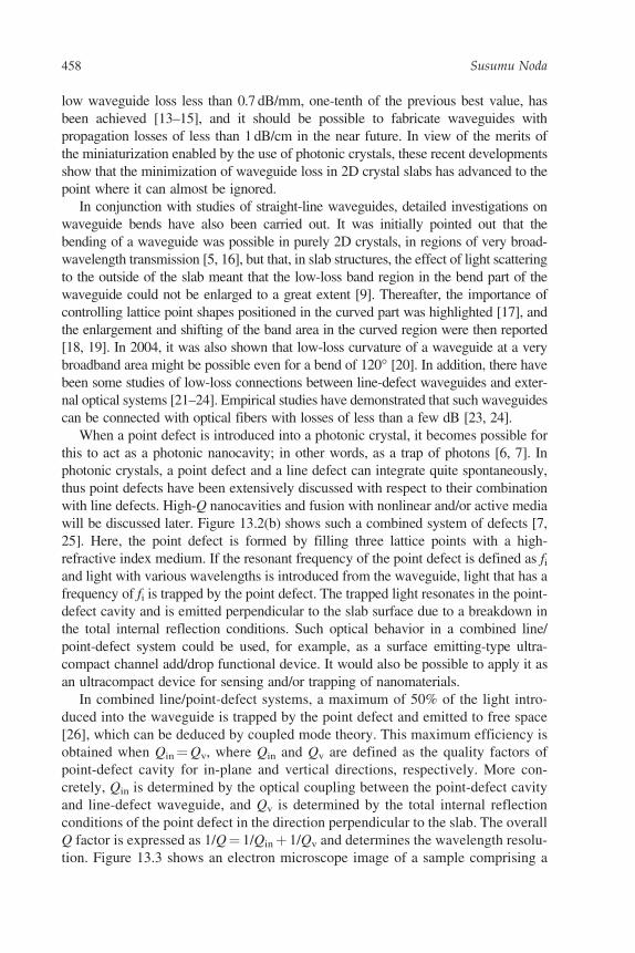
tion. Figure 13.3 shows an electron microscope image of a sample comprising a
458 Susumu Noda
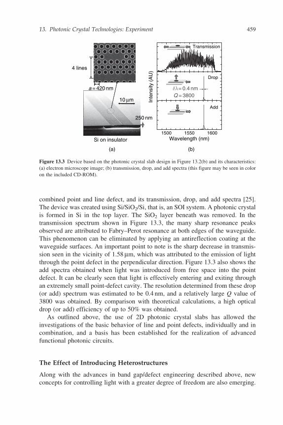
combined point and line defect, and its transmission, drop, and add spectra [25].
The device was created using Si/SiO2/Si, that is, an SOI system. A photonic crystal
is formed in Si in the top layer. The SiO2 layer beneath was removed. In the
transmission spectrum shown in Figure 13.3, the many sharp resonance peaks
observed are attributed to Fabry–Perot resonance at both edges of the waveguide.
This phenomenon can be eliminated by applying an antireflection coating at the
waveguide surfaces. An important point to note is the sharp decrease in transmis-
sion seen in the vicinity of 1.58 mm, which was attributed to the emission of light
through the point defect in the perpendicular direction. Figure 13.3 also shows the
add spectra obtained when light was introduced from free space into the point
defect. It can be clearly seen that light is effectively entering and exiting through
an extremely small point-defect cavity. The resolution determined from these drop
(or add) spectrum was estimated to be 0.4 nm, and a relatively large Q value of
3800 was obtained. By comparison with theoretical calculations, a high optical
drop (or add) efficiency of up to 50% was obtained.
As outlined above, the use of 2D photonic crystal slabs has allowed the
investigations of the basic behavior of line and point defects, individually and in
combination, and a basis has been established for the realization of advanced
functional photonic circuits.
The Effect of Introducing Heterostructures
Along with the advances in band gap/defect engineering described above, new
concepts for controlling light with a greater degree of freedom are also emerging.
(a) (b)
1500 1550 1600Wavelength (nm)
Inte
nsity
(A
U)
Transmission
Drop
Add
δλ = 0.4 nmQ = 3800
10 μm
4 lines
a = 420 nm
250 nm
Si on insulator
Figure 13.3 Device based on the photonic crystal slab design in Figure 13.2(b) and its characteristics:
(a) electron microscope image; (b) transmission, drop, and add spectra (this figure may be seen in color
on the included CD-ROM).
13. Photonic Crystal Technologies: Experiment 459
One of these is the fabrication of photonic crystal heterostructures [27, 28]. In the
field of semiconductor electronics, the fundamental technology involving hetero-
structures is concerned with optical/electronic devices such as laser diodes and
transistors, the importance of which does not need elaboration here. However,
in addition to their functions in electronic systems, heterostructures are also
playing important, albeit different, roles in photonic crystal research. The purpose
of developing heterostructures in photonic crystals is explained below using an in-
plane heterostructure [27] in a 2D crystal slab.
Figure 13.4 shows an example of an in-plane heterostructure. This photonic
crystal has the same basic structure as that shown in Figure 13.3, except that the
lattice constant has been slightly varied to give seven different values. Figure 13.4
also shows an electron microscope image of each part of the sample actually
created. The schematic drawing emphasizes the variation in lattice constant, but
in the fabricated sample the lattice constant in adjacent areas differed by only
1.25 nm, too small to be discerned from the electron microscope image. One of
the promising properties of this type of in-plane heterostructure is the possibility of
obtaining an optimized multiwavelength behavior while maintaining the high
values of Q (3800) and high drop efficiency (50%) for the configuration shown in
Figure 13.3. As described in the previous section, the overall point-defect Q value is
determined by a combination of the in-plane value Qin and the vertical value Qv,
and the radiation efficiency is highest when Qin = Qv. If the size of only one point
defect is changed, in turn changing the operational wavelength, the effective
PC1
Optical input(λ 1, λ 2,..., λ 7)
PC7 PC6
a7 = 418.75 nm a6 = 417.5 nm a2 = 412.5 nm a1 = 411.25 nmHeterointerface
PC5 PC2
Lattice constant difference
Heterointerface
1.25 nm
λ 7
λ 6
λ 1
Figure 13.4 Example of an in-plane heterostructure: The insets show electron microscope images of a
fabricated sample. The schematic drawing highlights the differences in lattice constant, which is too
small (1.25 nm) to see in the microscope images (this figure may be seen in color on the included
CD-ROM).
460 Susumu Noda
refractive index of the defect will also be altered, resulting in a change in Qv.
However, Qin will be relatively unaffected; therefore, the overall Q value will be
altered and the drop efficiency will change together with the wavelength. The
difference in the overall Q value will also cause a change in the wavelength
resolution. When a heterostructure such as that in Figure 13.4 is used to vary the
structure of the overall crystal proportionally, although the operating wavelength
will change with the lattice constant, the Q value and drop efficiency, which are
dimensionless quantities, will be maintained at constant values. In other words,
multiwavelength operations will be possible as long as the wavelength resolution
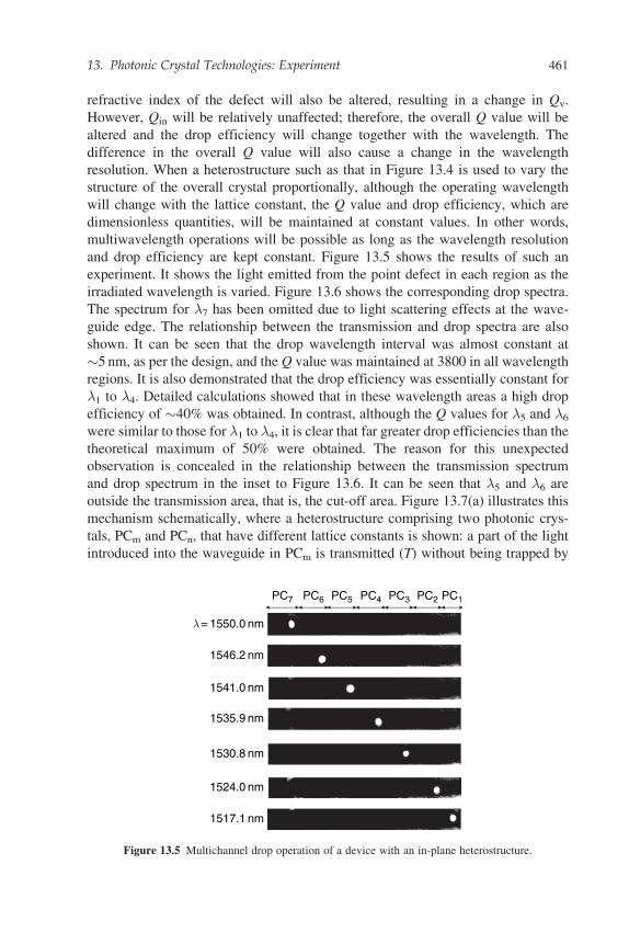
and drop efficiency are kept constant. Figure 13.5 shows the results of such an
experiment. It shows the light emitted from the point defect in each region as the
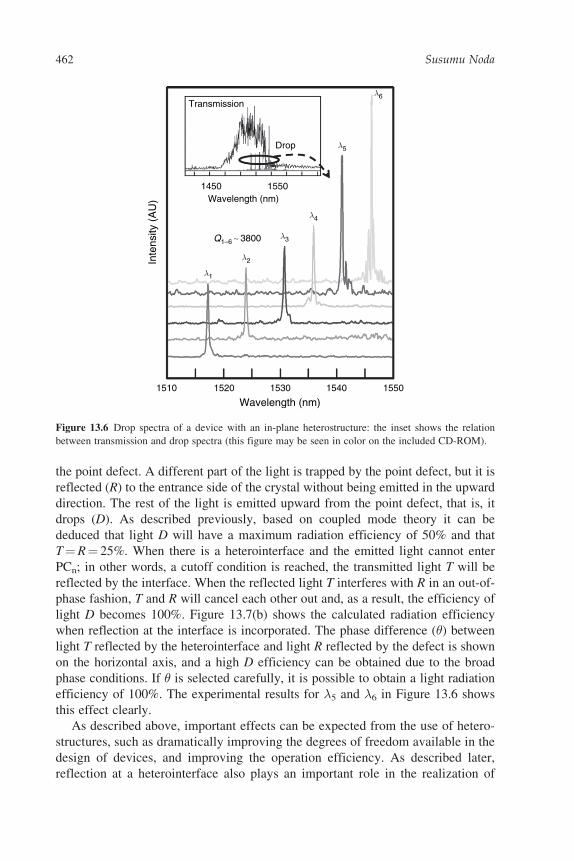
irradiated wavelength is varied. Figure 13.6 shows the corresponding drop spectra.
The spectrum for �7 has been omitted due to light scattering effects at the wave-
guide edge. The relationship between the transmission and drop spectra are also
shown. It can be seen that the drop wavelength interval was almost constant at
�5 nm, as per the design, and the Q value was maintained at 3800 in all wavelength
regions. It is also demonstrated that the drop efficiency was essentially constant for
�1 to �4. Detailed calculations showed that in these wavelength areas a high drop
efficiency of �40% was obtained. In contrast, although the Q values for �5 and �6
were similar to those for �1 to �4, it is clear that far greater drop efficiencies than the
theoretical maximum of 50% were obtained. The reason for this unexpected
observation is concealed in the relationship between the transmission spectrum
and drop spectrum in the inset to Figure 13.6. It can be seen that �5 and �6 are
outside the transmission area, that is, the cut-off area. Figure 13.7(a) illustrates this
mechanism schematically, where a heterostructure comprising two photonic crys-
tals, PCm and PCn, that have different lattice constants is shown: a part of the light
introduced into the waveguide in PCm is transmitted (T) without being trapped by
PC7 PC6 PC5
λ = 1550.0 nm
1546.2 nm
1541.0 nm
1535.9 nm
1530.8 nm
1524.0 nm
1517.1 nm
PC4 PC3 PC2 PC1
Figure 13.5 Multichannel drop operation of a device with an in-plane heterostructure.
13. Photonic Crystal Technologies: Experiment 461
the point defect. A different part of the light is trapped by the point defect, but it is
reflected (R) to the entrance side of the crystal without being emitted in the upward
direction. The rest of the light is emitted upward from the point defect, that is, it
drops (D). As described previously, based on coupled mode theory it can be
deduced that light D will have a maximum radiation efficiency of 50% and that
T = R = 25%. When there is a heterointerface and the emitted light cannot enter
PCn; in other words, a cutoff condition is reached, the transmitted light T will be
reflected by the interface. When the reflected light T interferes with R in an out-of-
phase fashion, T and R will cancel each other out and, as a result, the efficiency of
light D becomes 100%. Figure 13.7(b) shows the calculated radiation efficiency
when reflection at the interface is incorporated. The phase difference (�) between
light T reflected by the heterointerface and light R reflected by the defect is shown
on the horizontal axis, and a high D efficiency can be obtained due to the broad
phase conditions. If � is selected carefully, it is possible to obtain a light radiation
efficiency of 100%. The experimental results for �5 and �6 in Figure 13.6 shows
this effect clearly.
As described above, important effects can be expected from the use of hetero-
structures, such as dramatically improving the degrees of freedom available in the
design of devices, and improving the operation efficiency. As described later,
reflection at a heterointerface also plays an important role in the realization of
λ 2
λ 1
λ 6
λ 5
λ 4
λ 3Q1–6 ∼ 3800
Drop
15501450Wavelength (nm)
Transmission
1510 1520 1530 1540 1550
Inte
nsity
(A
U)
Wavelength (nm)
Figure 13.6 Drop spectra of a device with an in-plane heterostructure: the inset shows the relation
between transmission and drop spectra (this figure may be seen in color on the included CD-ROM).
462 Susumu Noda
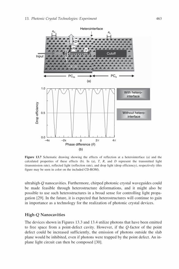
ultrahigh-Q nanocavities. Furthermore, chirped photonic crystal waveguides could
be made feasible through heterostructure deformations, and it might also be
possible to use such heterostructures in a broad sense for controlling light propa-
gation [29]. In the future, it is expected that heterostructures will continue to gain
in importance as a technology for the realization of photonic crystal devices.
High-Q Nanocavities
The devices shown in Figures 13.3 and 13.4 utilize photons that have been emitted
to free space from a point-defect cavity. However, if the Q-factor of the point
defect could be increased sufficiently, the emission of photons outside the slab
plane would be inhibited, even if photons were trapped by the point defect. An in-
plane light circuit can then be composed [30].
am an
RT
D
PCnPCm
With hetero-interface
CutoffInput
Heterointerface
Without hetero-interface
Dro
p ef
ficie
ncy
Phase difference (θ )
(a)
Cancel
(b)
1.0
0.5
0.0–4π –2π 0 2π 4π
Figure 13.7 Schematic drawing showing the effects of reflection at a heterointerface (a) and the
calculated properties of these effects (b). In (a), T, R, and D represent the transmitted light
(transmission rate), reflected light (reflection rate), and drop light (drop efficiency), respectively (this
figure may be seen in color on the included CD-ROM).
13. Photonic Crystal Technologies: Experiment 463
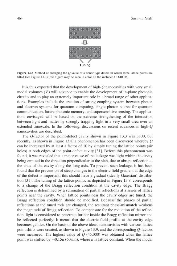
It is thus expected that the development of high-Q nanocavities with very small
modal volumes (V ) will advance to enable the development of in-plane photonic
circuits and to play an extremely important role in a broad range of other applica-
tions. Examples include the creation of strong coupling system between photon
and electron systems for quantum computing, single photon source for quantum
communication, future photonic memory, and supersensitive sensing. The applica-
tions envisaged will be based on the extreme strengthening of the interaction
between light and matter by strongly trapping light in a very small area over an
extended timescale. In the following, discussions on recent advances in high-Q
nanocavities are described.
The Q-factor of the point-defect cavity shown in Figure 13.3 was 3800, but
recently, as shown in Figure 13.8, a phenomenon has been discovered whereby Q
can be increased by at least a factor of 10 by simply tuning the lattice points (air
holes) at both edges of the point-defect cavity [31]. Before this phenomenon was
found, it was revealed that a major cause of the leakage was light within the cavity
being emitted in the direction perpendicular to the slab, due to abrupt reflection at
the ends of the cavity along the long axis. To prevent such leakage, it has been
found that the prevention of steep changes in the electric field gradient at the edge
of the defect is important: this should have a gradual (ideally Gaussian) distribu-
tion [31]. The tuning of the lattice points, as depicted in Figure 13.8, corresponds
to a change of the Bragg reflection condition at the cavity edge. The Bragg
reflection is determined by a summation of partial reflections at a series of lattice
points near the cavity. When lattice points near the cavity edges are tuned, the
Bragg reflection condition should be modified. Because the phases of partial
reflections at the tuned rods are changed, the resultant phase-mismatch weakens
the magnitude of Bragg reflection. To compensate for the reduction of the reflec-
tion, light is considered to penetrate further inside the Bragg reflection mirror and
be reflected perfectly. It means that the electric field profile at the cavity edge
becomes gentler. On the basis of the above ideas, nanocavities with various lattice
point shifts were created, as shown in Figure 13.9, and the corresponding Q-factors
were measured. The highest value of Q (45,000) was obtained when the lattice
point was shifted by �0.15a (60 nm), where a is lattice constant. When the modal
Tuning
Figure 13.8 Method of enlarging the Q-value of a donor-type defect in which three lattice points are
filled (see Figure 13.3) (this figure may be seen in color on the included CD-ROM).
464 Susumu Noda
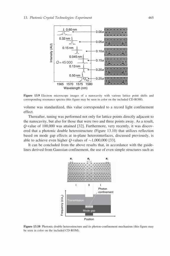
volume was standardized, this value corresponded to a record light confinement
effect.
Thereafter, tuning was performed not only for lattice points directly adjacent to
the nanocavity, but also for those that were two and three points away. As a result,
Q-value of 100,000 was attained [32]. Furthermore, very recently, it was discov-
ered that a photonic double heterostructure (Figure 13.10) that utilizes reflection
based on mode gap effects at in-plane heterointerfaces, discussed previously, is
able to achieve even higher Q-values of �1,000,000 [33].
It can be concluded from the above results that, in accordance with the guide-
lines derived from Gaussian confinement, the use of even simple structures such as
1565 1570 1575 1580Wavelength (nm)
0.00a
0.05a
0.10a
0.15a
0.20a
0.25a
0.60 nm
0.32 nm
0.15 nm
0.045 nm
0.13 nm
0.50 nm
Inte
nsity
(A
U)
Q = 45 000
Figure 13.9 Electron microscope images of a nanocavity with various lattice point shifts and
corresponding resonance spectra (this figure may be seen in color on the included CD-ROM).
Position
Mode gap
Transmission
Photon confinement
Fre
quen
cy (
c/a
2)
a1 a2 a1
IIII
Figure 13.10 Photonic double heterostructure and its photon-confinement mechanism (this figure may
be seen in color on the included CD-ROM).
13. Photonic Crystal Technologies: Experiment 465
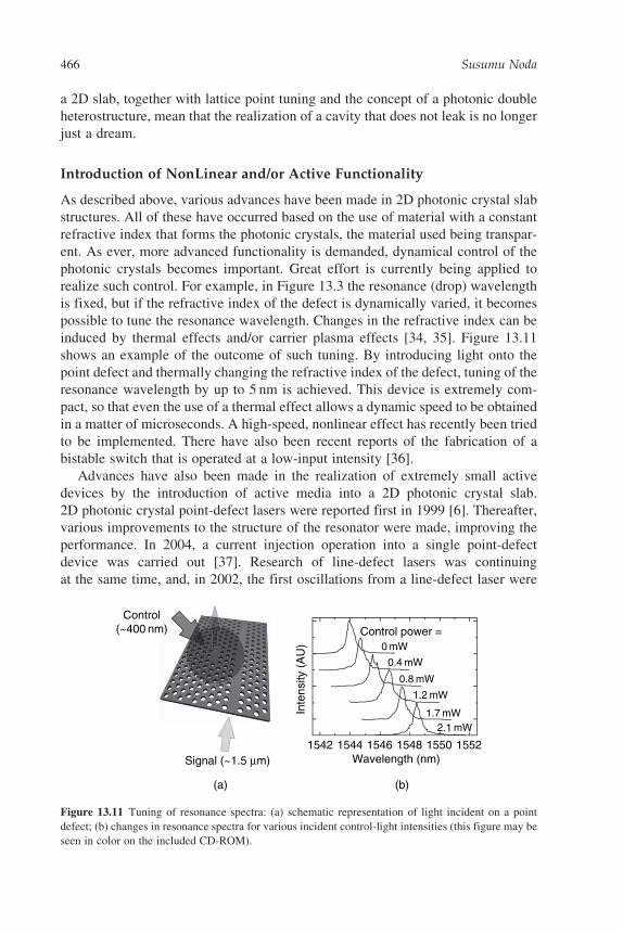
a 2D slab, together with lattice point tuning and the concept of a photonic double
heterostructure, mean that the realization of a cavity that does not leak is no longer
just a dream.
Introduction of NonLinear and/or Active Functionality
As described above, various advances have been made in 2D photonic crystal slab
structures. All of these have occurred based on the use of material with a constant
refractive index that forms the photonic crystals, the material used being transpar-
ent. As ever, more advanced functionality is demanded, dynamical control of the
photonic crystals becomes important. Great effort is currently being applied to
realize such control. For example, in Figure 13.3 the resonance (drop) wavelength
is fixed, but if the refractive index of the defect is dynamically varied, it becomes
possible to tune the resonance wavelength. Changes in the refractive index can be
induced by thermal effects and/or carrier plasma effects [34, 35]. Figure 13.11
shows an example of the outcome of such tuning. By introducing light onto the
point defect and thermally changing the refractive index of the defect, tuning of the
resonance wavelength by up to 5 nm is achieved. This device is extremely com-
pact, so that even the use of a thermal effect allows a dynamic speed to be obtained
in a matter of microseconds. A high-speed, nonlinear effect has recently been tried
to be implemented. There have also been recent reports of the fabrication of a
bistable switch that is operated at a low-input intensity [36].
Advances have also been made in the realization of extremely small active
devices by the introduction of active media into a 2D photonic crystal slab.
2D photonic crystal point-defect lasers were reported first in 1999 [6]. Thereafter,
various improvements to the structure of the resonator were made, improving the
performance. In 2004, a current injection operation into a single point-defect
device was carried out [37]. Research of line-defect lasers was continuing
at the same time, and, in 2002, the first oscillations from a line-defect laser were
Control(~400 nm)
Signal (~1.5 μm)
Control power =
Inte
nsity
(A
U)
Wavelength (nm)
0 mW
0.4 mW
0.8 mW
1.2 mW
1.7 mW2.1 mW
(a) (b)
1542 1544 1546 1548 1550 1552
Figure 13.11 Tuning of resonance spectra: (a) schematic representation of light incident on a point
defect; (b) changes in resonance spectra for various incident control-light intensities (this figure may be
seen in color on the included CD-ROM).
466 Susumu Noda
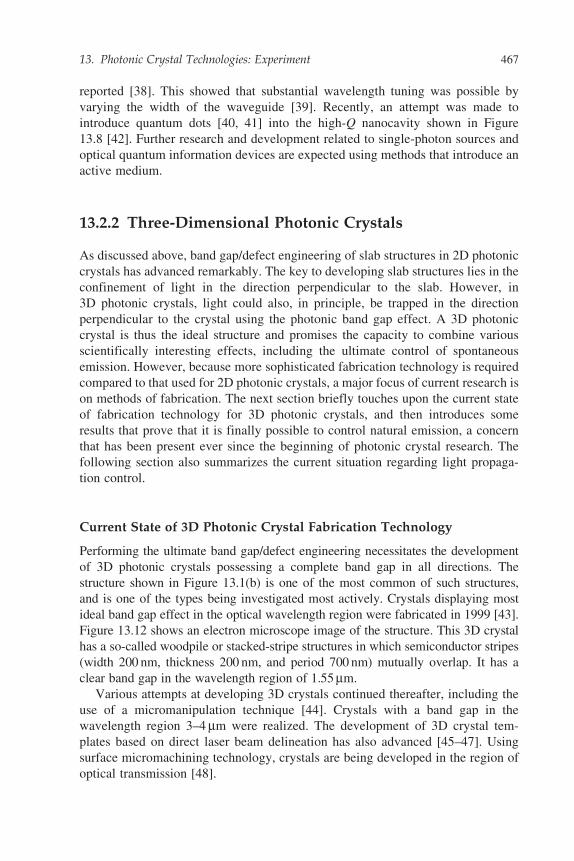
reported [38]. This showed that substantial wavelength tuning was possible by
varying the width of the waveguide [39]. Recently, an attempt was made to
introduce quantum dots [40, 41] into the high-Q nanocavity shown in Figure
13.8 [42]. Further research and development related to single-photon sources and
optical quantum information devices are expected using methods that introduce an
active medium.
13.2.2 Three-Dimensional Photonic Crystals
As discussed above, band gap/defect engineering of slab structures in 2D photonic
crystals has advanced remarkably. The key to developing slab structures lies in the
confinement of light in the direction perpendicular to the slab. However, in
3D photonic crystals, light could also, in principle, be trapped in the direction
perpendicular to the crystal using the photonic band gap effect. A 3D photonic
crystal is thus the ideal structure and promises the capacity to combine various
scientifically interesting effects, including the ultimate control of spontaneous
emission. However, because more sophisticated fabrication technology is required
compared to that used for 2D photonic crystals, a major focus of current research is
on methods of fabrication. The next section briefly touches upon the current state
of fabrication technology for 3D photonic crystals, and then introduces some
results that prove that it is finally possible to control natural emission, a concern
that has been present ever since the beginning of photonic crystal research. The
following section also summarizes the current situation regarding light propaga-
tion control.
Current State of 3D Photonic Crystal Fabrication Technology
Performing the ultimate band gap/defect engineering necessitates the development
of 3D photonic crystals possessing a complete band gap in all directions. The
structure shown in Figure 13.1(b) is one of the most common of such structures,
and is one of the types being investigated most actively. Crystals displaying most
ideal band gap effect in the optical wavelength region were fabricated in 1999 [43].
Figure 13.12 shows an electron microscope image of the structure. This 3D crystal
has a so-called woodpile or stacked-stripe structures in which semiconductor stripes
(width 200 nm, thickness 200 nm, and period 700 nm) mutually overlap. It has a
clear band gap in the wavelength region of 1.55 mm.
Various attempts at developing 3D crystals continued thereafter, including the
use of a micromanipulation technique [44]. Crystals with a band gap in the
wavelength region 3–4 mm were realized. The development of 3D crystal tem-
plates based on direct laser beam delineation has also advanced [45–47]. Using
surface micromachining technology, crystals are being developed in the region of
optical transmission [48].
13. Photonic Crystal Technologies: Experiment 467
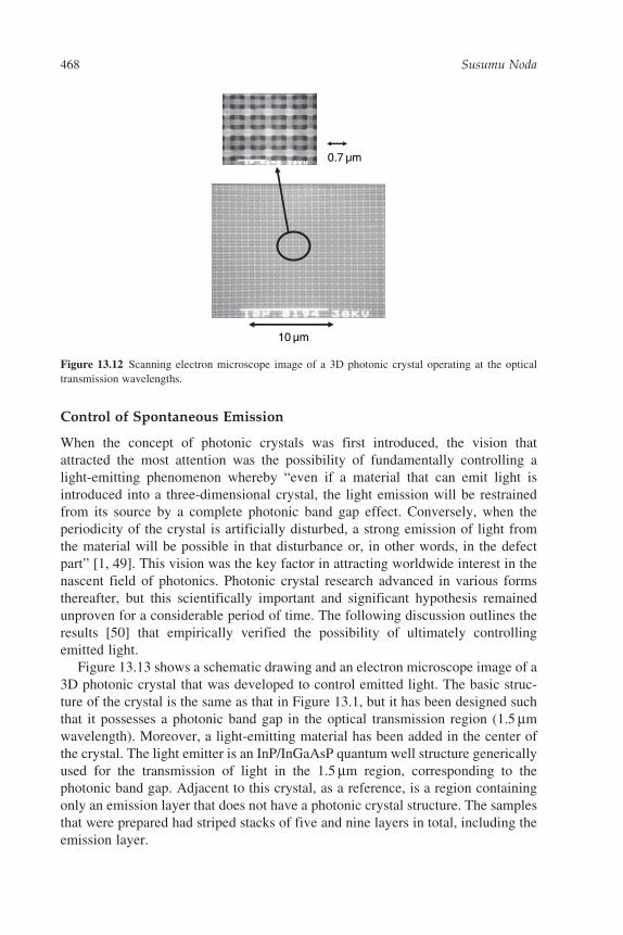
Control of Spontaneous Emission
When the concept of photonic crystals was first introduced, the vision that
attracted the most attention was the possibility of fundamentally controlling a
light-emitting phenomenon whereby “even if a material that can emit light is
introduced into a three-dimensional crystal, the light emission will be restrained
from its source by a complete photonic band gap effect. Conversely, when the
periodicity of the crystal is artificially disturbed, a strong emission of light from
the material will be possible in that disturbance or, in other words, in the defect
part” [1, 49]. This vision was the key factor in attracting worldwide interest in the
nascent field of photonics. Photonic crystal research advanced in various forms
thereafter, but this scientifically important and significant hypothesis remained
unproven for a considerable period of time. The following discussion outlines the
results [50] that empirically verified the possibility of ultimately controlling
emitted light.
Figure 13.13 shows a schematic drawing and an electron microscope image of a
3D photonic crystal that was developed to control emitted light. The basic struc-
ture of the crystal is the same as that in Figure 13.1, but it has been designed such
that it possesses a photonic band gap in the optical transmission region (1.5 mm
wavelength). Moreover, a light-emitting material has been added in the center of
the crystal. The light emitter is an InP/InGaAsP quantum well structure generically
used for the transmission of light in the 1.5 mm region, corresponding to the
photonic band gap. Adjacent to this crystal, as a reference, is a region containing
only an emission layer that does not have a photonic crystal structure. The samples
that were prepared had striped stacks of five and nine layers in total, including the
emission layer.
0.7 µm
10 µm
Figure 13.12 Scanning electron microscope image of a 3D photonic crystal operating at the optical
transmission wavelengths.
468 Susumu Noda
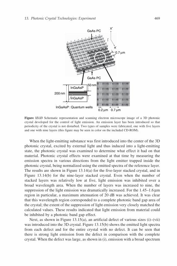
When the light-emitting substance was first introduced into the center of the 3D
photonic crystal, excited by external light and thus induced into a light-emitting
state, the photonic crystal was examined to determine what effect it had on that
material. Photonic crystal effects were examined at that time by measuring the
emission spectra in various directions from the light emitter trapped inside the
photonic crystal, being normalized using the emitted spectra of the reference layer.
The results are shown in Figure 13.14(a) for the five-layer stacked crystal, and in
Figure 13.14(b) for the nine-layer stacked crystal. Even when the number of
stacked layers was relatively low at five, light emission was inhibited over a
broad wavelength area. When the number of layers was increased to nine, the
suppression of the light emission was dramatically increased. For the 1.45–1.6 mm
region in particular, a maximum attenuation of 20 dB was achieved. It was clear
that this wavelength region corresponded to a complete photonic band gap area of
the crystal; the extent of the suppression of light emission very closely matched the
calculated values. These results indicated that light emission from material could
be inhibited by a photonic band gap effect.
Next, as shown in Figure 13.15(a), an artificial defect of various sizes (i)–(vii)
was introduced into the 3D crystal. Figure 13.15(b) shows the emitted light spectra
from each defect and for the entire crystal with no defect. It can be seen that
there is strong light emission from the defect in comparison with the complete
crystal. When the defect was large, as shown in (i), emission with a broad spectrum
200 nm
50 nm
InGaAsP : Quantum wells
0.7 μm
GaAs PC
GaAs PC
0.2 μm 0.7 μm
⎡
X′
K
InGaAsP
InGaAsP
Figure 13.13 Schematic representation and scanning electron microscope image of a 3D photonic
crystal developed for the control of light emission. An emission layer has been introduced so that
periodicity of the crystal is not disturbed. Two types of samples were fabricated, one with five layers
and one with nine layers (this figure may be seen in color on the included CD-ROM).
13. Photonic Crystal Technologies: Experiment 469
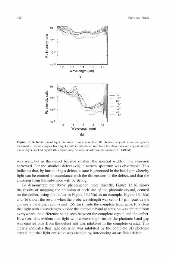
was seen, but as the defect became smaller, the spectral width of the emission
narrowed. For the smallest defect (vii), a narrow spectrum was observable. This
indicates that, by introducing a defect, a state is generated in the band gap whereby
light can be emitted in accordance with the dimensions of the defect, and that the
emission from the substance will be strong.
To demonstrate the above phenomenon more directly, Figure 13.16 shows
the results of mapping the emission at each site of the photonic crystal, centred
on the defect, using the defect in Figure 13.15(a) as an example. Figure 13.16(a)
and (b) shows the results when the probe wavelength was set to 1.3 mm (outside the
complete band gap region) and 1.55 mm (inside the complete band gap). It is clear
that light with a wavelength outside the complete band gap region was emitted from
everywhere, no difference being seen between the complete crystal and the defect.
However, it is evident that light with a wavelength inside the photonic band gap
was emitted only from the defect and was inhibited in the complete crystal. This
clearly indicates that light emission was inhibited by the complete 3D photonic
crystal, but that light emission was enabled by introducing an artificial defect.
0°10°–10°20°–20°30°–30°40°–40°
1.2 1.3 1.4 1.5 1.6
10–1
10–2
10–3
10
PL
inte
nsity
rat
io
10–1
10–2
10–3
10
PL
inte
nsity
rat
io
(b)
(a)
Wavelength (μm)
1.2 1.3 1.4 1.5 1.6
Wavelength (μm)
Figure 13.14 Inhibition of light emission from a complete 3D photonic crystal: emission spectra
measured at various angles from light emitters introduced into (a) a five-layer stacked crystal and (b)
a nine-layer stacked crystal (this figure may be seen in color on the included CD-ROM).
470 Susumu Noda
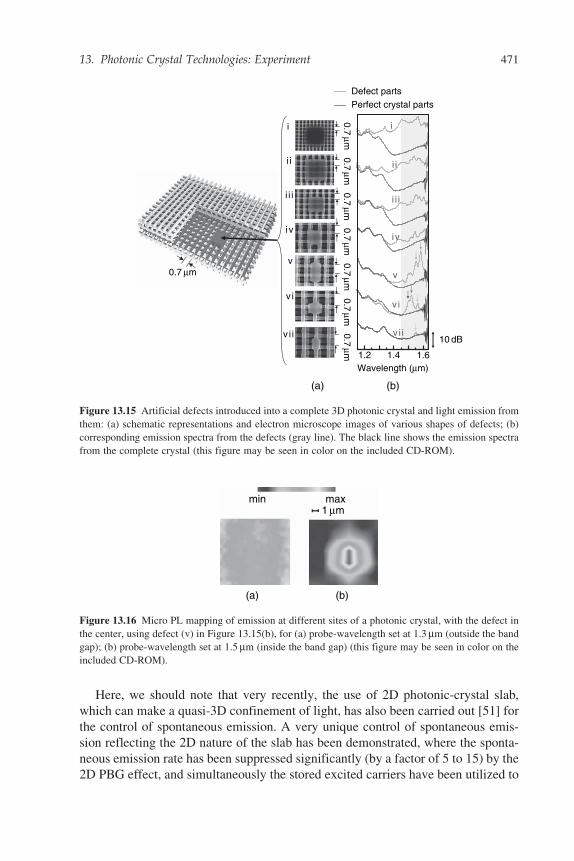
Here, we should note that very recently, the use of 2D photonic-crystal slab,
which can make a quasi-3D confinement of light, has also been carried out [51] for
the control of spontaneous emission. A very unique control of spontaneous emis-
sion reflecting the 2D nature of the slab has been demonstrated, where the sponta-
neous emission rate has been suppressed significantly (by a factor of 5 to 15) by the
2D PBG effect, and simultaneously the stored excited carriers have been utilized to
min max1 μm
(a) (b)
Figure 13.16 Micro PL mapping of emission at different sites of a photonic crystal, with the defect in
the center, using defect (v) in Figure 13.15(b), for (a) probe-wavelength set at 1.3 mm (outside the band
gap); (b) probe-wavelength set at 1.5 mm (inside the band gap) (this figure may be seen in color on the
included CD-ROM).
0.7 μm
0.7 μm
0.7 μm
0.7 μm
0.7 μm
0.7 μm
0.7 μm
0.7 μm
iv
vi
iii
ii
i
iiv
v
Wavelength (μm)1.2 1.4 1.6
10 dB
i
ii
iii
vi
iv
iiv
v
Defect partsPerfect crystal parts
(b)(a)
Figure 13.15 Artificial defects introduced into a complete 3D photonic crystal and light emission from
them: (a) schematic representations and electron microscope images of various shapes of defects; (b)
corresponding emission spectra from the defects (gray line). The black line shows the emission spectra
from the complete crystal (this figure may be seen in color on the included CD-ROM).
13. Photonic Crystal Technologies: Experiment 471
emit light to the direction normal to the photonic-crystal plane where the PBG
effect does not exist.
Control of Light Propagation
As discussed in “Control of Light by Combined Line/Point-Defect Systems”
research on line-defect waveguides in 2D photonic crystal slabs has advanced
remarkably. However, light propagation [52] has recently been observed also in
3D photonic crystals. Figure 13.17(a) shows a schematic drawing of a fabricated
defect waveguide, created by thickening a single stripe in a 3D crystal. A similar
3D crystal structure to that discussed previously was used and, for the defect part,
the single stripe width was thicker than its surroundings. Figure 13.17(b) shows a
scanning electron microscope image of a five-layer state in which one GaAs
striped layer including the waveguide was fused with a four-layer photonic crystal.
Figure 13.17(c) shows a scanning electron microscope image of a cross section of
the crystal after its completion. It is clearly shown that a 3D photonic crystal
waveguide has been successfully formed. A light propagation experiment on the
fabricated samples verified that light can be propagated in a wavelength band of
5 μm
5 μm
(c)(b)
(a)
Figure 13.17 3D photonic-crystal waveguide: (a) schematic representation of a fabricated waveguide;
(b) electron microscope image of the surface of a five-layer configuration in which a four-layer photonic
crystal was combined with a single GaAs striped layer containing a waveguide; (c) scanning electron
microscope image of a cross section of the 3D waveguide after fabrication (this figure may be seen in
color on the included CD-ROM).
472 Susumu Noda
1.5 mm [53]. This experiment represented the first successful propagation of light
in a fiber optic wavelength region in 3D crystals. Currently, the number of layers
that have been stacked is about nine, so the propagation loss is still relatively large,
but it is expected that an increase in the number of layers will cause the propaga-
tion loss to decrease exponentially.
13.3 BAND EDGE ENGINEERING
13.3.1 Outline of Resonance Action at the Band Edge
As is well known, distributed feedback semiconductor lasers have a 1D periodic
lattice. The propagating waves undergo Bragg diffraction from this lattice and are
diffracted in the opposite direction. As a result, the propagating waves merge with
the diffracted waves, which in turn causes a standing wave to be set up and a
resonator to be formed. This is equivalent to providing a state in which the
resonator loss is minimized at the band edge of 1D photonic crystal band gaps,
which enables oscillation [54]. By incorporating this idea into the development of
photonic crystals with 2D lattices and utilizing the combination of several light
waves by Bragg diffraction within the 2D plane, it becomes possible to compose a
stable wave state that extends throughout the entire plane [55]. As a result, it is
possible to obtain an oscillation mode in which the electromagnetic distribution is
fully controlled at each lattice point of the 2D crystal. In other words, it would be
possible in a 2D crystal to regulate, not only the longitudinal mode for the laser
oscillation, but also the beam pattern—the so-called transverse mode. It would
thus be possible to create a laser that could oscillate in single longitudinal and
transverse modes at any time, irrespective of the size of the area, and would be
possible to create a completely new laser that goes beyond conventional concepts.
Oscillation using current injection based on these principles was first realized in
1999 [55]. Research into the laser action of light pumping using organic dyes has
also advanced [56, 57]. Recently, resonators based on this principle have been used
in the field of quantum cascade lasers [58]. This shows promise as a powerful laser
resonator system in 2D photonic slabs with an introduced active medium [59, 60].
Another feature of devices based on this principle is that the formation of band
gaps is unnecessary: such devices can therefore be envisaged for various types of
active media and crystal structures.
13.3.2 Broad Area Coherent Laser Action
Figure 13.18 shows an example of a laser structure based on band edge engineer-
ing [60–63]. This laser comprises two wafers, A and B. Wafer A includes an active
layer, on top of which a photonic crystal has been introduced. By joining wafer A
with wafer B, the photonic crystal is enclosed, thereby completing the device.
13. Photonic Crystal Technologies: Experiment 473
The actual material used is an InGaAs/GaAs semiconductor. As can be seen in the
inset to Figure 13.18, the photonic crystals used have a square lattice structure and
are set up such that the lattice period in the G–X direction matches the emitted
wavelength in the active layer. Light propagated in a specific G–X direction will be
diffracted both in the opposite direction (–180�) and at angles of –90� and 90�. The
resulting four equivalent light waves will be combined, causing a 2D resonator to
form. Figure 13.19(a) shows the corresponding band structure. The resonance
Active
Fusion
Γ–X
Γ–M
–180°
–90° 90°
Wafer B
Wafer A
0°
Figure 13.18 Laser structure constructed by band edge engineering (this figure may be seen in color on the
included CD-ROM).
X
k// k//
Fre
quen
cy
X M
Bandedge
A
B
C
D
980
960
940
920
Wav
elen
gth
(nm
)
(a)
(b)
MX
Γ Γ
Γ
M X
Figure 13.19 (a) Calculated and (b) measured band structures for 2D photonic crystal laser (this figure
may be seen in color on the included CD-ROM).
474 Susumu Noda
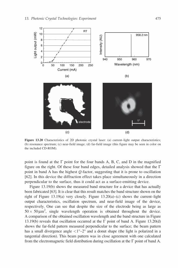
point is found at the G point for the four bands A, B, C, and D in the magnified
figure on the right. Of these four band edges, detailed analysis showed that the Gpoint in band A has the highest Q-factor, suggesting that it is prone to oscillation
[62]. In this device the diffraction effect takes place simultaneously in a direction
perpendicular to the surface, thus it could act as a surface-emitting device.
Figure 13.19(b) shows the measured band structure for a device that has actually
been fabricated [63]. It is clear that this result matches the band structure shown on the
right of Figure 13.19(a) very closely. Figure 13.20(a)–(c) shows the current–light
output characteristics, oscillation spectrum, and near-field image of the device,
respectively. One can see that despite the size of the electrode being as large as
50� 50 mm2, single wavelength operation is obtained throughout the device.
A comparison of the obtained oscillation wavelength and the band structure in Figure
13.19(b) reveals that oscillation occurred at the G point of band A. Figure 13.20(d)
shows the far-field pattern measured perpendicular to the surface; the beam pattern
has a small divergence angle <1�–2� and a donut shape (the light is polarized in a
tangential direction). This beam pattern was in close agreement with one calculated
from the electromagnetic field distribution during oscillation at the G point of band A.
Current (mA)
0
2
4
6
8
10
12
0 50 100 150 200 250
RT
1°
958.2 nm
940 950 960 970
Wavelength (nm)
Inte
nsity
(A
U)
Lig
ht o
utpu
t (m
W)
(d)(c)
(b)(a)
electrode
Figure 13.20 Characteristics of 2D photonic crystal laser: (a) current–light output characteristics;
(b) resonance spectrum; (c) near-field image; (d) far-field image (this figure may be seen in color on
the included CD-ROM).
13. Photonic Crystal Technologies: Experiment 475
The investigations described above show that devices can be fabricated that
operate at the band edge of 2D photonic band structures and that operate in stable
single mode over large areas. The continuous room-temperature oscillation of such
a device has been realized [61].
13.3.3 Lattice Point Control and Polarization Mode Control
A donut-shaped far-field pattern has been obtained using a photonic crystal laser, as
shown in Figure 13.20(d). This type of beam shape is important for optical tweezers
[64] and other applications, such as a light source for omniguide photonic-crystal
fibers [65]. However, controlling the polarization mode and beam patterns would
be important steps for further expanding the range of applications for this laser.
In the following, some of the efforts made to achieve this are described.
Photonic crystals have various degrees of freedom, such as the shape of the
lattice points, the lattice intervals, and the construction of heterostructures as
discussed in “The Effect of Introducing Heterostructures.” By designing these
characteristics, it is possible to control the oscillation mode. In the case of lattice
points with a circular shape, as shown in the inset to Figure 13.18, four light waves
that propagate in a G–X direction are equivalent; in a state of resonance, a highly
symmetrical (i.e., rotationally symmetrical) electromagnetic field distribution
is thus achieved. Consequently, beams that are emitted in a direction perpendicular
to the surface possess the different polarized light components equivalently;
the polarized light does not become unidirectional. In the center of the pattern,
the electromagnetic field is cancelled out and the beam becomes donut-shaped.
Here let us consider that lattice point shape changes from round to elliptical.
The inset to Figure 13.18 shows that the coupled state of the waves progressing
in the 0� and 180� directions and the coupled state of the waves progressing in the
þ90� and –90� directions are modulated, which causes the symmetry of the in-
plane electromagnetic field to break down. As a result, the unidirectional polarized
light state is enhanced and the polarization mode becomes controllable [66].
Moreover, it has currently been demonstrated that it is possible to generate a
range of beam patterns based on more advanced engineering of photonic crystal
structures [67].
Although it has not been discussed here, band edge engineering can not only
enhance the characteristics of lasers as mentioned above, but also a range of
nonlinear optical effects over large areas. Various types of interesting advances
are therefore likely in the near future.
13.4 BAND ENGINEERING
This section discusses control of light by utilizing the dispersion relations
in the transmission bands of photonic crystals, where the utilization of the
476 Susumu Noda
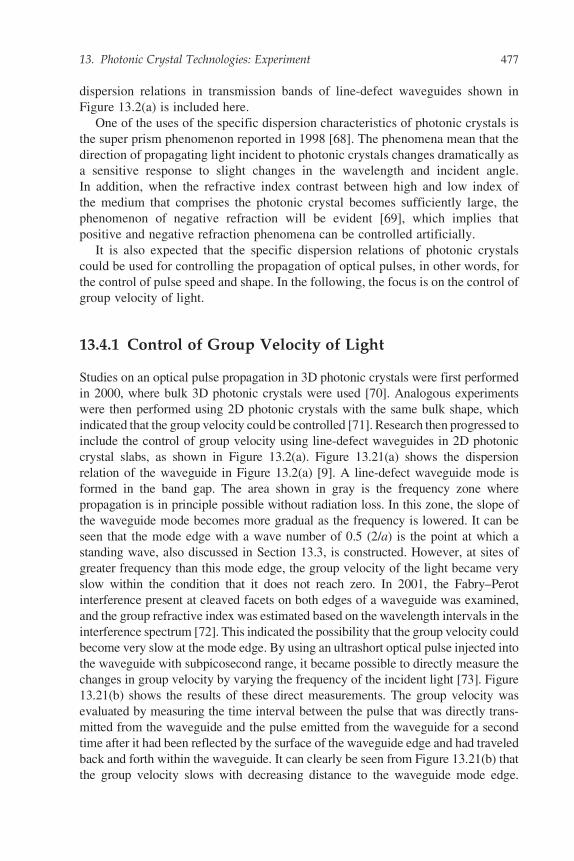
dispersion relations in transmission bands of line-defect waveguides shown in
Figure 13.2(a) is included here.
One of the uses of the specific dispersion characteristics of photonic crystals is
the super prism phenomenon reported in 1998 [68]. The phenomena mean that the
direction of propagating light incident to photonic crystals changes dramatically as
a sensitive response to slight changes in the wavelength and incident angle.
In addition, when the refractive index contrast between high and low index of
the medium that comprises the photonic crystal becomes sufficiently large, the
phenomenon of negative refraction will be evident [69], which implies that
positive and negative refraction phenomena can be controlled artificially.
It is also expected that the specific dispersion relations of photonic crystals
could be used for controlling the propagation of optical pulses, in other words, for
the control of pulse speed and shape. In the following, the focus is on the control of
group velocity of light.
13.4.1 Control of Group Velocity of Light
Studies on an optical pulse propagation in 3D photonic crystals were first performed
in 2000, where bulk 3D photonic crystals were used [70]. Analogous experiments
were then performed using 2D photonic crystals with the same bulk shape, which
indicated that the group velocity could be controlled [71]. Research then progressed to
include the control of group velocity using line-defect waveguides in 2D photonic
crystal slabs, as shown in Figure 13.2(a). Figure 13.21(a) shows the dispersion
relation of the waveguide in Figure 13.2(a) [9]. A line-defect waveguide mode is
formed in the band gap. The area shown in gray is the frequency zone where
propagation is in principle possible without radiation loss. In this zone, the slope of
the waveguide mode becomes more gradual as the frequency is lowered. It can be
seen that the mode edge with a wave number of 0.5 (2/a) is the point at which a
standing wave, also discussed in Section 13.3, is constructed. However, at sites of
greater frequency than this mode edge, the group velocity of the light became very
slow within the condition that it does not reach zero. In 2001, the Fabry–Perot
interference present at cleaved facets on both edges of a waveguide was examined,
and the group refractive index was estimated based on the wavelength intervals in the
interference spectrum [72]. This indicated the possibility that the group velocity could
become very slow at the mode edge. By using an ultrashort optical pulse injected into
the waveguide with subpicosecond range, it became possible to directly measure the
changes in group velocity by varying the frequency of the incident light [73]. Figure
13.21(b) shows the results of these direct measurements. The group velocity was
evaluated by measuring the time interval between the pulse that was directly trans-
mitted from the waveguide and the pulse emitted from the waveguide for a second
time after it had been reflected by the surface of the waveguide edge and had traveled
back and forth within the waveguide. It can clearly be seen from Figure 13.21(b) that
the group velocity slows with decreasing distance to the waveguide mode edge.
13. Photonic Crystal Technologies: Experiment 477
As mentioned above, this phenomenon is expected to provide basic data relevant to
various applications, including pulse shaping and optical delay line function.
13.4.2 Angular Control of Light Propagation
It is easy to see that photonic crystals can play a role as diffraction gratings. By
actively utilizing this diffraction grating action, it becomes possible, for example,
to improve the light extraction efficiency of light-emitting diodes. From this
perspective, great effort is being invested in improving the efficiency of light-
emitting diodes using photonic crystal structures. Current interest is especially
focused on applications [74–77] for GaN system light-emitting diodes and organic
EL elements. The light-emitting efficiency of both of these instruments was
reportedly improved by a factor of �1.5 when photonic crystals were introduced.
For such applications, it is important to develop technology that allows photonic
0.26 0.27 0.28
0.2
0.1
0
a = 0.420 μm
a = 0.415 μm
a = 0.410 μm
Gro
up v
eloc
ity (
c)
Normalized frequency f/(c/a)
32 ps
8.5 ps
15 ps
0.10 0.2 0.3 0.4 0.5. .
0.34
0.32
0.3
0.28
0.26
Wavenumber (2π/a)
Fre
quen
cy (
c/a)
Light line
(a)
(b)–50 0 50
0.001
0.0050.01
0.050.1
0.51
Delay (ps)
Aut
ocor
rela
tion
inte
nsity
(A
U)
–50 0 500.001
0.0050.01
0.050.1
0.51
Delay (ps)A
utoc
orre
latio
nin
tens
ity (
AU
)
–50 0 500.001
0.0050.01
0.050.1
0.51
Delay (ps)
Aut
ocor
rela
tion
inte
nsity
(A
U)
Figure 13.21 Control of group velocity of a light pulse: (a) dispersion relation of the line-defect
waveguide in Figure 13.2(a). The right-hand line represents the boundary of the leakage of light that
propagates through the waveguide. There is no light leakage at frequencies equal to or lower than this
line. The value c on the longitudinal axis represents the speed of the light, and a represents the lattice
constant. (b) measured group velocity calculated using an autocorrelation method (this figure may be
seen in color on the included CD-ROM).
478 Susumu Noda
crystals to be easily formed. Integration with nanoprocessing techniques such as
nanoimprinting is also an extremely interesting development [78, 79].
13.5 SUMMARY AND FUTURE PROSPECTS
Recent advances in photonic crystals have been discussed in terms of (i) band gap and
defect engineering, (ii) band edge engineering, and (iii) band engineering. Although
many of the explanations given may have been insufficient due to space limitations, it
is hoped that the reader has come away with a sense of the steady advances made in
the last few years in fundamental technology for operating and controlling light in
extremely small volumes, which was the initial expectation of photonic crystals.
It is expected that, over the next 10 years, nanoprocessing technology will
dramatically advance, and that more reliable and precise devices will continue to
be developed. In the case of 2D photonic crystal slabs, there is promise of remarkable
advances in Si-based systems, together with progress in integration with electronic
circuits. Further advances can be expected in combined optical and electronic
circuits equipped with features such as optical switching, tuning, and delay function-
ality. It is expected that the main components of such circuits will be optical, and
optical/electronic chips will be developed. There is no doubt that the size and power
consumption of such devices will be more than tens to hundreds of times smaller than
they are now. Advances in a large number of applications can also be expected,
including developments in next generation miniaturized multiple-wavelength light
sources based on the addition of active functionality, supersensitive sensors, optical
memory functions that require a high Q-value, and single photon light sources.
It is expected that band edge lasers will enable surface emission over a large
area with a single wavelength, single light polarization, and single spot, and that by
controlling the photonic crystal structure the beam pattern will also be fully
controllable. It is likely that band edge lasers will be applied in future to a wide
range of fields including information processing, communications, and bio-related
fields. It is believed that progress in integrating photonic crystals with organic EL
and blue LED devices will also be made, and that important advances will occur in
highly efficient emission diodes and display technology.
It is expected that the technology available for the fabrication of 3D photonic
crystals, which are considered to be more difficult to fabricate than 2D crystals at
the present time, will also advance over the coming decade, and that 3D crystals
will witness completely new levels of light control that will also enable intricate
“complete control of fields.”
ACKNOWLEDGMENT
This work was supported by the Core Research for Evolutional Science and
Technology (CREST) program of the Japan Science and Technology Agency, by
13. Photonic Crystal Technologies: Experiment 479
a Grant-in-Aid for Scientific Research of the Ministry of Education, Culture,
Sports, Science and Technology of Japan, by the Global COE program of Kyoto
University.
REFERENCES
[1] E. Yablonovitch, “Applied physics - How to be truly photonic,” Science, 289, 557–559, 2000.
[2] S. Noda and T. Baba (eds), Roadmap on Photonic Crystals, Kluwer Academic Publishers,
Springer, 2003.
[3] K. M. Ho, C. T. Chan, and C. M. Soukoulis, “Existence of a photonic gap in periodic dielectric
structures,” Phys. Rev. Lett., 65, 3152–3155, 1990.
[4] S. Noda, N. Yamamoto, and A. Sasaki, “New realization method for three-dimensional photonic
crystal in optical wavelength region,” Jpn. J. Appl. Phys., 35, L909–L912, 1996.
[5] J. D. Joannopoulos, P. R. Villeneuve, and S. Fan, “Photonic crystals: Putting a new twist on light,”
Nature, 386, 143–149, 1997.
[6] O. Painter, R. K. Lee, A. Scherer et al., “Two-dimensional photonic band-gap defect mode laser,”
Science, 284, 1819–1821, 1999.
[7] S. Noda, A. Chutinan, and M. Imada, “Trapping and emission of photons by a single defect in a
photonic bandgap structure,” Nature, 407, 608–610, 2000.
[8] T. Baba, N. Fukaya, and J. Yonekura, “Observation of light propagation in photonic crystal optical
waveguides with bends,” Electron. Lett., 35, 654–655, 1999.
[9] A. Chutinan and S. Noda, “Waveguides and waveguide bends in two-dimensional photonic crystal
slabs,” Phys. Rev. B, 62, 4488–4492, 2000.
[10] M. Notomi, A. Shinya, K. Yamada et al., “Singlemode transmission within photonic bandgap of
width-varied single-line-defect photonic crystal waveguides on SOI substrates,” Electron. Lett.,
37, 293–295, 2001.
[11] Y. Tanaka, T. Asano, Y. Akahane et al., “Theoretical investigation of a two-dimensional photonic
crystal slab with truncated cone air holes,” Appl. Phys. Lett., 82, 1661–1663, 2003.
[12] S. Takayama, H. Kitagawa, T. Asano et al., “Experimental demonstration of complete photonic
band gap in two-dimensional photonic crystal slabs,” Appl. Phys. Lett., 87, Art. No. 061107, 2005.
[13] S. J. McNab, N. Moll, and Y. A. Vlasov, “Ultra-low loss photonic integrated circuit with
membrane-type photonic crystal waveguides,” Opt. Express, 11, 2927–2939, 2003.
[14] Y. Sugimoto, Y. Tanaka, N. Ikeda et al., “Low propagation loss of 0.76 dB/mm in GaAs-based
single-line-defect two-dimensional photonic crystal slab waveguides up to 1 cm in length,”
Opt. Express, 12, 1090–1096, 2004.
[15] E. Kuramochi, M. Notomi, S. Hughes et al., “Disorder-induced scattering loss of line-defect
waveguides in photonic crystal slabs,” Phys. Rev. B, 72, Art. No. 161318, 2005.
[16] A. Mekis, J. C. Chen, I. Kurland et al., “High transmission through sharp bends in photonic crystal
waveguides,” Phys. Rev. Lett., 77, 3787–3790, 1996.
[17] A. Chutinan, M. Okano, and S. Noda, “Wider bandwidth with high transmission through wave-
guide bends in two-dimensional photonic crystal slabs,” Appl. Phys. Lett., 80, 1698–1700, 2002.
[18] Y. Sugimoto, Y. Tanaka, N. Ikeda et al., “Two dimensional semiconductor-based photonic crystal
slab waveguides for ultra-fast optical signal processing devices,” IEICE Trans. Electron., 87C,
316–327, 2004.
[19] H. Takano, Y. Akahane, T. Asano, and S. Noda, “In-plane-type channel drop filter in a
two-dimensional photonic crystal slab,” Appl. Phys. Lett., 84, 2226–2228, 2004.
[20] P. I. Borel, A. Harpoth, L. H. Frandsen et al., “Topology optimization and fabrication of photonic
crystal structures,” Opt. Express, 12, 1996–2001, 2004.
[21] E. Miyai, M. Okano, M. Mochizuki, and S. Noda, “Analysis of coupling between two-dimensional
photonic crystal waveguide and external waveguide,” Appl. Phys. Lett., 81, 3729–3731, 2002;
480 Susumu Noda
E. Miyai and S. Noda, “Structural dependence of coupling between a two-dimensional photonic
crystal waveguide and a wire waveguide,” J. Opt. Soc. Am. B, 21, 67–72, 2004.
[22] A. Gomyo, J. Ushida, M. Shirane et al., “Low optical loss connection for photonic crystal slab
waveguides,” IEICE Trans. Electron., E87C, 328–335, 2004.
[23] T. Shoji, T. Tsuchizawa, T. Watanabe et al., “Low loss mode size converter from 0.3 mm square
Si wire waveguides to singlemode fibres,” Electron. Lett., 38, 1669–1670, 2002.
[24] M. Notomi, A. Shinya, S. Mitsugi et al., “Waveguides, resonators and their coupled elements in
photonic crystal slabs,” Opt. Express, 12, 1551–1561, 2004.
[25] Y. Akahane, T. Asano, B. S. Song, and S. Noda, “Investigation of high-Q channel drop
filters using donor-type defects in two-dimensional photonic crystal slabs,” Appl. Phys. Lett.,
83, 1512–1514, 2003.
[26] A. Chutinan, M. Mochizuki, M. Imada, and S. Noda, “Surface-emitting channel drop filters using
single defects in two-dimensional photonic crystal slabs,” Appl. Phys. Lett., 79, 2690–2692, 2001.
[27] B. S. Song, S. Noda, and T. Asano, “Photonic devices based on in-plane hetero photonic crystals,”
Science, 300, 1537, 2003.
[28] S. Kawakami, T. Sato, K. Miura et al., “3-D photonic-crystal hetero structures: Fabrication and
in-line resonator,” IEEE Photon. Technol. Lett., 15, 816–818, 2003.
[29] D. Mori and T. Baba, “Dispersion-controlled optical group delay device by chirped photonic
crystal waveguides,” Appl. Phys. Lett., 85, 1101–1103, 2004.
[30] H. Takano, Y. Akahane, T. Asano, and S. Noda, “In-plane-type channel drop filter in a two-
dimensional photonic crystal slab,” Appl. Phys. Lett., 84, 2226–2228, 2004; H. Takano, B. S. Song,
T. Asano, and S. Noda, “Highly efficient multi-channel drop filter in a two-dimensional hetero
photonic crystal,” Opt. Express, 14, 3492–3496, 2006.
[31] Y. Akahane, T. Asano, B. S. Song, and S. Noda, “High-Q photonic nanocavity in a two-dimen-
sional photonic crystal,” Nature, 425, 944–947, 2003.
[32] Y. Akahane, T. Asano, B. S. Song, and S. Noda, “Fine-tuned high-Q photonic-crystal nanocavity,”
Opt. Express, 13, 1202–1214, 2005.
[33] B.S. Song, S. Noda, and T. Asano, “Ultra-high-Q photonic double-heterostructure nanocavity,”
Nat. Mater., 4, 207–210, 2005; T. Asano, B. S. Song, and S. Noda, “Analysis of the experimental Q
factors (similar to 1 million) of photonic crystal nanocavities,” Opt. Express, 14, 1996–2002, 2006.
[34] T. Asano, W. Kunishi, M. Nakamura et al., “Dynamic wavelength tuning of channel-drop device
in two-dimensional photonic crystal slab,” Electron. Lett., 41, 37–38, 2005.
[35] T. Baba, M. Shiga, K. Inoshita, and F. Koyama, “Carrier plasma shift in GaInAsP photonic crystal
point defect cavity,” Electron. Lett., 39, 1516–1518, 2003.
[36] M. Notomi, A. Shinya, S. Mitsugi et al., “Optical bistable switching action of Si high-Q photonic-
crystal nanocavities,” Opt. Express, 13, 2678–2687, 2005.
[37] H. G. Park, S. H. Kim, S. H. Kwon et al., “Electrically driven single-cell photonic crystal laser,”
Science, 305, 1444–1447, 2004.
[38] A. Sugitatsu and S. Noda, “Room temperature operation of 2D photonic crystal slab defect-
waveguide laser with optical pump,” Electron. Lett., 39, 123–125, 2003.
[39] A. Sugitatsu, T. Asano, and S. Noda, “Characterization of line-defect-waveguide lasers in
two-dimensional photonic-crystal slabs,” Appl. Phys. Lett., 84, 5395–5397, 2004.
[40] Y. Arakawa and H. Sakaki, “Multidimensional quantum well laser and temperature-dependence of
its threshold current,” Appl. Phys. Lett., 40, 939–941, 1982.
[41] M. Tabuchi, S. Noda, and A. Sasaki, “Mesoscopic structure in lattice-mismatched heteroepitaxial
interface layers,” Science and Technology of Mesoscopic Structures edited by Nanba et al.,
1992, pp. 379–384; Y. Nabetani, T. Ishikawa, S. Noda, and A. Sasaki, “Initial growth stage and
optical-properties of a 3-dimensional inas structure on gaas,” J. Appl. Phys., 76, 347–351, 1994.
[42] T. Yoshie, A. Scherer, J. Hendrickson et al., “Vacuum Rabi splitting with a single quantum dot in a
photonic crystal nanocavity,” Nature, 432, 200–203, 2004.
[43] S. Noda, K. Tomoda, N. Yamamoto, and A. Chutinan, “Full three-dimensional photonic bandgap
crystals at near-infrared wavelengths,” Science, 289, 604–606, 2000.
13. Photonic Crystal Technologies: Experiment 481
[44] K. Aoki, H. T. Miyazaki, H. Hirayama et al., “Microassembly of semiconductor three-dimensional
photonic crystals,” Nat. Mater., 2, 117–121, 2003.
[45] M. Campbell, D. N. Sharp, M. T. Harrison et al., “Fabrication of photonic crystals for the visible
spectrum by holographic lithography,” Nature, 404, 53–56, 2000.
[46] V. Mizeikis, K. K. Seet, S. Juodkazis, and H. Misawa, “Three-dimensional woodpile photonic
crystal templates for the infrared spectral range,” Opt. Lett., 29, 2061–2063, 2004.
[47] M. Deubel, G. V. Freymann, M. Wegener et al., “Direct laser writing of three-dimensional
photonic-crystal templates for telecommunications,” Nat. Mater., 3, 444–447, 2004.
[48] M. Qi, E. Lidorikis, P. T. Rakich et al., “A three-dimensional optical photonic crystal with
designed point defects,” Nature, 429, 538–542, 2004.
[49] E. Yablonovitch, “Inhibited spontaneous emission in solid-state physics and electronics,” Phys.
Rev. Lett., 58, 2059–2062, 1987.
[50] S. Ogawa, M. Imada, S. Yoshimoto et al., “Control of light emission by 3D photonic crystals,”
Science, 305, 227–229, 2004 (Published online 3 June 2004 (10.1126/science.1097968)).
[51] M. Fujita, S. Takahashi, Y. Tanaka et al., “Simultaneous inhibition and redistribution of sponta-
neous light emission in photonic crystals,” Science, 308, 1296–1298, 2005; K. Kounoike,
M. Yamaguchi, M. Fujita et al., “Investigation of spontaneous emission from quantum dots
embedded in two-dimensional photonic-crystal slab,” Electron. Lett., 41, 1402–1403, 2005.
[52] A. Chutinan and S. Noda, “Highly confined waveguides and waveguide bends in three-dimensional
photonic crystal,” Appl. Phys. Lett., 75, 3739–3741, 1999; M. Okano, S. Kako, and S. Noda,
“Coupling between a point-defect cavity and a line-defect waveguide in three-dimensional photonic
crystal,” Phys. Rev. B, 68, Art. No. 235110, 2003.
[53] M. Imada, L. H. Lee, M. Okano et al., “Development of three-dimensional photonic-crystal
waveguides at optical-communication wavelengths,” Appl. Phys. Lett., 88, Art. No. 171107, 2006.
[54] H. Kogelnik and C. V. Shank, “Coupled-wave theory of distributed feedback lasers,” J. Appl.
Phys., 43, 2327–2335, 1972.
[55] M. Imada, S. Noda, A. Chutinan et al., “Coherent two-dimensional lasing action in surface-
emitting laser with triangular-lattice photonic crystal structure,” Appl. Phys. Lett., 75, 316–318,
1999; M. Imada, A. Chutinan, S. Noda, and M. Mochizuki, “Multidirectionally distributed feed-
back photonic crystal lasers,” Phys. Rev. B, 65, Art. No. 195306, 2002.
[56] M. Meier, A. Mekis, A. Dodabalapur et al., “Laser action from two-dimensional distributed
feedback in photonic crystals,” Appl. Phys. Lett., 74, 7–9, 1999.
[57] M. Notomi, H. Suzuki, and T. Tamamura, “Directional lasing oscillation of two-dimensional organic
photonic crystal lasers at several photonic band gaps,” Appl. Phys. Lett., 78, 1325–1327, 2001.
[58] R. Colombelli, K. Srinivasan, M. Troccoli et al., “Quantum cascade surface-emitting photonic
crystal laser,” Science, 302, 1374–1377, 2003.
[59] S. H. Kwon, S. H. Kim, S. K. Kim et al., “Small, low-loss heterogeneous photonic bandedge
laser,” Opt. Express, 12, 5356–5361, 2004.
[60] D. Ohnishi, K. Sakai, M. Imada, and S. Noda, “Continuous wave operation of surface emitting
two-dimensional photonic crystal laser,” Electron. Lett., 39, 612–614, 2003.
[61] D. Ohnishi, T. Okano, M. Imada, and S. Noda, “Room temperature continuous wave operation of a
surface-emitting two-dimensional photonic crystal diode laser,” Opt. Express, 12, 1562–1568,
2004.
[62] M. Yokoyama and S. Noda, “Finite-difference time-domain simulation of two-dimensional photo-
nic crystal surface-emitting laser having a square-lattice slab structure,” IEICE Trans. Electron.,
E87C, 386–392, 2004.
[63] K. Sakai, D. Ohnishi, T. Okano et al., “Lasing band-edge identification for a surface-emitting
photonic crystal laser,” IEEE J. Sel. Area Commun., 23, 1335–1340, 2005.
[64] A. Ashkin, “History of optical trapping and manipulation of small-neutral particle, atoms, and
molecules,” IEEE J. Sel. Top. Quantum Electron., 6, 841–856, 2000.
[65] Y. Fink, D. J. Ripin, S. H. Fan et al., “Guiding optical light in air using an all-dielectric structure,”
J. Lightw. Technol., 17, 2039–2041, 1999.
482 Susumu Noda
[66] S. Noda, M. Yokoyama, M. Imada et al., “Polarization mode control of two-dimensional photonic
crystal laser by unit cell structure design,” Science, 293, 1123–1125, 2001.
[67] E. Miyai1, K. Sakai1, T. Okano et al., “Lasers producing tailored beams,” Nature, 441, 946, 2006.
[68] H. Kosaka, T. Kawashima, A. Tomita et al., “Superprism phenomena in photonic crystals,” Phys.
Rev. B, 58, R10096–R10099, 1998.
[69] M. Notomi, “Theory of light propagation in strongly modulated photonic crystals: Refractionlike
behavior in the vicinity of the photonic band gap,” Phys. Rev. B, 62, 10696–10705, 2000.
[70] T. Tanaka, S. Noda, A. Chutinan et al., “Ultra-short pulse propagation in 3D GaAs photonic
crystals,” Technical Digest of International Workshop on Photonic and Electromagnetic Crystal
Structure (PESC-II), W4–14, 2000; Opt. Quantum Electron., 34, 37–43, 2002.
[71] K. Inoue, N. Kawai, Y. Sugimoto et al., “Observation of small group velocity in two-dimensional
AlGaAs-based photonic crystal slabs,” Phys. Rev. B, 65, Art. No. 121308, 2002.
[72] M. Notomi, K. Yamada, A. Shinya et al., “Extremely large group-velocity dispersion of line-defect
waveguides in photonic crystal slabs,” Phys. Rev. Lett., 87, Art. No. 253902, 2001.
[73] T. Asano, K. Kiyota, D. Kumamoto et al., “Time-domain measurement of picosecond light-pulse
propagation in a two-dimensional photonic crystal-slab waveguide,” Appl. Phys. Lett., 84,
4690–4692, 2004.
[74] K. Orita, S. Tamura, T. Takizawa et al., “High-extraction-efficiency blue light-emitting diode
using extended-pitch photonic crystal,” Jpn. J. Appl. Phys., 43, 5809–5813, 2004.
[75] M. Fujita, T. Ueno, T. Asano et al., “Organic light-emitting diode with ITO/organic photonic
crystal,” Electron. Lett., 39, 1750–1752, 2003.
[76] Y. R. Do, Y. C. Kim, Y. W. Song et al., “Enhanced light extraction from organic light-emitting
diodes with 2D SiO2/SiNx photonic crystals,” Adv. Mater., 15, 1214–1218, 2003.
[77] M. Fujita, T. Ueno, K. Ishihara et al., “Reduction of operating voltage in organic light-emitting
diode by corrugated photonic crystal structure,” Appl. Phys. Lett., 85, 5769–5771, 2004.
[78] A. Yokoo, H. Suzuki, and M. Notomi, “Organic photonic crystal band edge laser fabricated by
direct nanoprinting,” Jpn. J. Appl. Phys., 43, 4009–4011, 2004.
[79] K. Ishihara, M. Fujita, I. Matsubara et al., “Direct fabrication of photonic crystal on glass substrate
by nanoimprint lithography,” Jpn. J. Appl. Phys., 45, L210–L212, 2006.
13. Photonic Crystal Technologies: Experiment 483
14Photonic crystal fibers: Basicsand applications
Philip St John Russell
Max-Planck Research Group (IOIP)University of Erlangen-Nuremberg, Erlangen, Germany
14.1 INTRODUCTION
Photonic crystal fibers (PCFs)—fibers with a periodic transverse microstructure—
first emerged as practical low-loss waveguides in early 1996 [1, 2]. The initial
demonstration took 4 years of technological development, and since then the
fabrication techniques have become more and more sophisticated. It is now
possible to manufacture the microstructure in air–glass PCF to accuracies of 10 nm
on the scale of 1 mm, which allows remarkable control of key optical properties
such as dispersion, birefringence, nonlinearity, and the position and width of the
photonic band gaps (PBGs) in the periodic “photonic crystal” cladding. PCF has
in this way extended the range of possibilities in optical fibers, both by improv-
ing well-established properties and by introducing new features such as low-loss
guidance in a hollow core.
In this chapter, the properties of the various types of PCF (the main classes of
PCF structure are illustrated in Figure 14.1) are first introduced, followed by a
detailed discussion of their established or emerging applications. An account of the
basic characteristics of PCF is available in [3].
14.2 FABRICATION TECHNIQUES
Photonic crystal fiber structures are currently produced in many laboratories
worldwide using a variety of different techniques (see Figure 14.2 for some
example structures). The first stage is to produce a “preform”—a macroscopic
version of the planned microstructure in the drawn PCF. There are many ways to
do this, including stacking of capillaries and rods [4], extrusion [5–8], sol-gel
Optical Fiber Telecommunications V A: Components and Subsystems
Copyright � 2008, Elsevier Inc. All rights reserved.
ISBN: 978-0-12-374171-4 485
b
a
c
d
e
g
f
Figure 14.1 Representative sketches of different types of PCF. The black regions are hollow, the white
regions are pure glass, and the grey regions are doped glass. (a) highly nonlinear PCF (high-air-filling
fraction, small core); (b) endlessly single-mode solid-core PCF; (c) double-clad PCF with offset doped
lasing core and high-numerical aperture inner cladding for pumping (the photonic crystal cladding is
held in place by thin webs of glass); (d) birefringent PCF; (e) dual-solid-core PCF; (f) 19-cell hollow-
core PCF; (g) hollow-core PCF with a Kagome cladding lattice. PBG-guiding all-solid glass versions of
(b) have been made in which the hollow channels are replaced with raised-index doped glass strands.
Figure 14.2 Selection of scanning electron micrographs of PCF structures. (a) The first working PCF—
the solid glass core is surrounded by a triangular array of 300-nm-diameter air channels, spaced 2.3 mm
apart [4]; (b) endlessly single-mode solid-core PCF (interhole spacing �2 mm; Erlangen); (c)
polarization-preserving solid-core PCF (Erlangen); (d) the first hollow-core PCF [11]; (e) a PCF
extruded from Schott SF6 glass with a core �2 mm in diameter [7]; (f) highly nonlinear PCF (core
diameter 800 nm [12]); (g) hollow-core PCF with Kagome lattice (Erlangen); (h) hollow-core PCF
guiding by a PBG (core diameter 20 mm; BlazePhotonics Limited); (i) detail of (h).
486 Philip St John Russell
casting [9], injection molding, and drilling. The materials used ranged from silica
to compound glasses, chalcogenide glasses, and polymers [10].
The most widely used technique is stacking of circular capillaries. Typically,
meter-length capillaries with an outer diameter of �1 mm are drawn from a
starting tube of high-purity synthetic silica with a diameter of �20 mm. The
inner/outer diameter of the starting tube, which typically lies in the range from
0.3 up to beyond 0.9, largely determines the d/L (hole diameter to spacing ratio)
value in the drawn fiber. The capillaries are stacked horizontally, in a suitably
shaped jig, to form the desired crystalline arrangement. The stack is bound with
wire before being inserted into a jacketing tube, and the whole assembly is then
mounted in the preform feed unit for drawing down to fiber. Judicious use of
pressure and vacuum during the draw allows some limited control over the final
structural parameters, for example, the d/L value.
14.2.1 Design Approach
The successful design of a PCF for a particular application is not simply a matter of
using numerical modeling to calculate the parameters of a structure that yields the
required performance. This is because the fiber-drawing process is not lithographic,
but introduces its own (highly reproducible) types of distortion through the effects of
viscous flow, surface tension, and pressure. As a result, even if the initial preform
stack precisely mimics the theoretically required structure, several modeling and
fabrication iterations are usually needed before a successful design can be reached.
14.3 CHARACTERISTICS OF PHOTONIC CRYSTALCLADDING
The simplest photonic crystal cladding is a biaxially periodic, defect-free, composite
material with its own well-defined dispersion and band structure. These properties
determine the behavior of the guided modes that form at cores (or “structural
defects” in the jargon of photonic crystals). A convenient graphical tool is the
propagation diagram—a map of the ranges of frequency and axial wavevector
component �, where light is evanescent in all transverse directions regardless of
its polarization state (Figure 14.3) [13]. The vertical axis is the normalized frequency
kL (vacuum wavevector k), and the horizontal axis is the normalized axial wave-
vector component �L. Light is unconditionally cutoff from propagating (due to
either total internal reflection (TIR) or PBG) in the black regions.
In any sub region of isotropic material (glass or air) at fixed optical frequency,
the maximum possible value of �L is given by kLn, where n is the refractive index
(at that frequency) of the region under consideration. For �< kn light is free to
propagate, for �> kn it is evanescent, and at �= kn the critical angle is reached—
denoting the onset of TIR for light incident from a medium of index larger than n.
14. Photonic Crystal Fibers: Basics and Applications 487
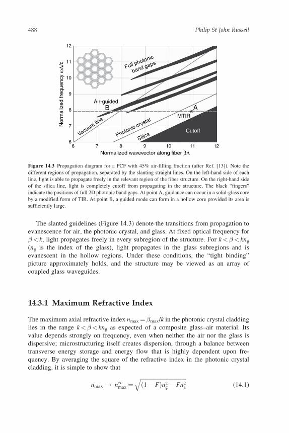
The slanted guidelines (Figure 14.3) denote the transitions from propagation to
evanescence for air, the photonic crystal, and glass. At fixed optical frequency for
� < k, light propagates freely in every subregion of the structure. For k<�< kng
(ng is the index of the glass), light propagates in the glass subregions and is
evanescent in the hollow regions. Under these conditions, the “tight binding”
picture approximately holds, and the structure may be viewed as an array of
coupled glass waveguides.
14.3.1 Maximum Refractive Index
The maximum axial refractive index nmax = �max/k in the photonic crystal cladding
lies in the range k<�< kng as expected of a composite glass–air material. Its
value depends strongly on frequency, even when neither the air nor the glass is
dispersive; microstructuring itself creates dispersion, through a balance between
transverse energy storage and energy flow that is highly dependent upon fre-
quency. By averaging the square of the refractive index in the photonic crystal
cladding, it is simple to show that
nmax ! n1max =ffiffiffiffiffiffiffiffiffiffiffiffiffiffiffiffiffiffiffiffiffiffiffiffiffiffiffiffiffiffiffiffiffið1� FÞn2
g � Fn2a
q(14.1)
12
11
10
9
8
7
66
Vacuum lin
e
Photonic crystal
Silica
7 8
Normalized wavevector along fiber βΛ
Nor
mal
ized
freq
uenc
y ω
Λ/c Full photonic
band gaps
Air-guided
9 10 11 12
Cutoff
MTIR
AB
Figure 14.3 Propagation diagram for a PCF with 45% air-filling fraction (after Ref. [13]). Note the
different regions of propagation, separated by the slanting straight lines. On the left-hand side of each
line, light is able to propagate freely in the relevant region of the fiber structure. On the right-hand side
of the silica line, light is completely cutoff from propagating in the structure. The black “fingers”
indicate the positions of full 2D photonic band gaps. At point A, guidance can occur in a solid-glass core
by a modified form of TIR. At point B, a guided mode can form in a hollow core provided its area is
sufficiently large.
488 Philip St John Russell
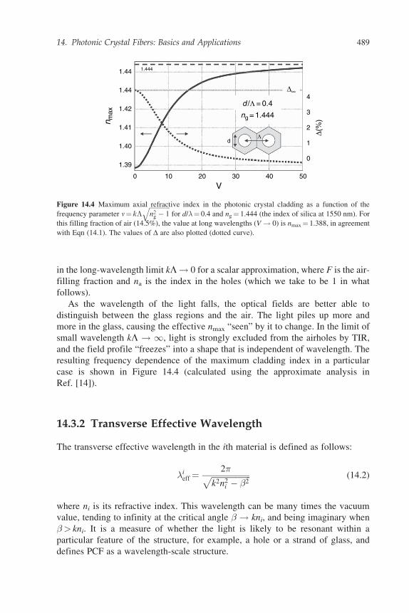
in the long-wavelength limit kL! 0 for a scalar approximation, where F is the air-
filling fraction and na is the index in the holes (which we take to be 1 in what
follows).
As the wavelength of the light falls, the optical fields are better able to
distinguish between the glass regions and the air. The light piles up more and
more in the glass, causing the effective nmax “seen” by it to change. In the limit of
small wavelength kL ! 1, light is strongly excluded from the airholes by TIR,
and the field profile “freezes” into a shape that is independent of wavelength. The
resulting frequency dependence of the maximum cladding index in a particular
case is shown in Figure 14.4 (calculated using the approximate analysis in
Ref. [14]).
14.3.2 Transverse Effective Wavelength
The transverse effective wavelength in the ith material is defined as follows:
�ieff =
2�ffiffiffiffiffiffiffiffiffiffiffiffiffiffiffiffiffiffiffiffik2n2
i � �2p (14.2)
where ni is its refractive index. This wavelength can be many times the vacuum
value, tending to infinity at the critical angle � ! kni, and being imaginary when
� > kni. It is a measure of whether the light is likely to be resonant within a
particular feature of the structure, for example, a hole or a strand of glass, and
defines PCF as a wavelength-scale structure.
1.44 1.444
1.44
1.42
1.41
1.40
1.39
0 10 20 30
V
n max
40 50
0
1
2
3
4d /Λ = 0.4
ng = 1.444
Δ(%
)
Δ∞
dΛ
Figure 14.4 Maximum axial refractive index in the photonic crystal cladding as a function of the
frequency parameter v= k�ffiffiffiffiffiffiffiffiffiffiffiffiffin2g � 1
qfor d/�= 0.4 and ng = 1.444 (the index of silica at 1550 nm). For
this filling fraction of air (14.5%), the value at long wavelengths (V! 0) is nmax = 1.388, in agreement
with Eqn (14.1). The values of D are also plotted (dotted curve).
14. Photonic Crystal Fibers: Basics and Applications 489
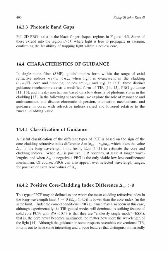
14.3.3 Photonic Band Gaps
Full 2D PBGs exist in the black finger-shaped regions in Figure 14.3. Some of
these extend into the region �< k, where light is free to propagate in vacuum,
confirming the feasibility of trapping light within a hollow core.
14.4 CHARACTERISTICS OF GUIDANCE
In single-mode fiber (SMF), guided modes form within the range of axial
refractive indices ncl< nz< nco, when light is evanescent in the cladding
(nz = �/k; core and cladding indices are nco and ncl). In PCF, three distinct
guidance mechanisms exist: a modified form of TIR [14, 15], PBG guidance
[11, 16], and a leaky mechanism based on a low density of photonic states in the
cladding [17]. In the following subsections, we explore the role of resonance and
antiresonance, and discuss chromatic dispersion, attenuation mechanisms, and
guidance in cores with refractive indices raised and lowered relative to the
“mean” cladding value.
14.4.1 Classification of Guidance
A useful classification of the different types of PCF is based on the sign of the
core-cladding refractive index difference D = (nco � ncl)/ncl, which takes the value
D1 in the long-wavelength limit [using Eqn (14.1) to estimate the core and
cladding indices]. When D1 is positive, TIR operates, at least at longer wave-
lengths, and when D1 is negative a PBG is the only viable low-loss confinement
mechanism. Of course, PBGs can also appear, over selected wavelength ranges,
for positive or even zero values of D1.
14.4.2 Positive Core-Cladding Index Difference D1 > 0
This type of PCF may be defined as one where the mean cladding refractive index in
the long-wavelength limit k ! 0 (Eqn (14.5)) is lower than the core index (in the
same limit). Under the correct conditions, PBG guidance may also occur in this case,
although experimentally the TIR-guided modes will dominate. A striking feature of
solid-core PCFs with d/L< 0.43 is that they are “endlessly single mode” (ESM),
that is, the core never becomes multimode, no matter how short the wavelength of
the light [14]. Although the guidance in some respects resembles conventional TIR,
it turns out to have some interesting and unique features that distinguish it markedly
490 Philip St John Russell
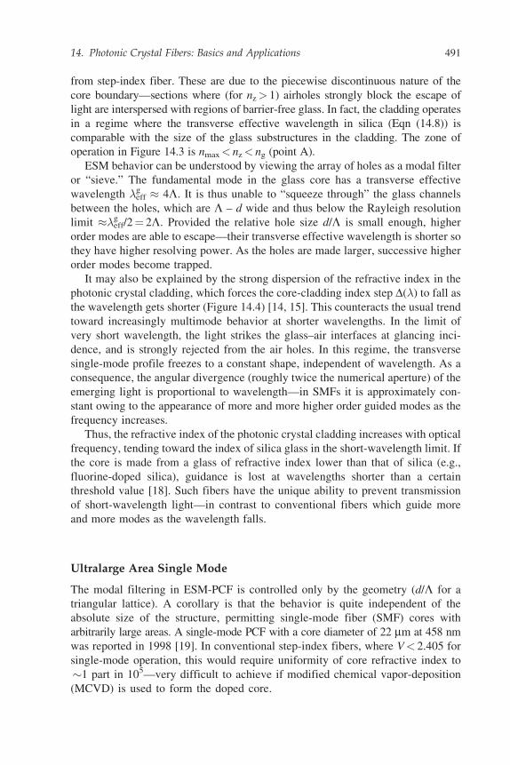
from step-index fiber. These are due to the piecewise discontinuous nature of the
core boundary—sections where (for nz> 1) airholes strongly block the escape of
light are interspersed with regions of barrier-free glass. In fact, the cladding operates
in a regime where the transverse effective wavelength in silica (Eqn (14.8)) is
comparable with the size of the glass substructures in the cladding. The zone of
operation in Figure 14.3 is nmax< nz< ng (point A).
ESM behavior can be understood by viewing the array of holes as a modal filter
or “sieve.” The fundamental mode in the glass core has a transverse effective
wavelength �effg � 4L. It is thus unable to “squeeze through” the glass channels
between the holes, which are L – d wide and thus below the Rayleigh resolution
limit ��effg /2 = 2L. Provided the relative hole size d/L is small enough, higher
order modes are able to escape—their transverse effective wavelength is shorter so
they have higher resolving power. As the holes are made larger, successive higher
order modes become trapped.
It may also be explained by the strong dispersion of the refractive index in the
photonic crystal cladding, which forces the core-cladding index step D(�) to fall as
the wavelength gets shorter (Figure 14.4) [14, 15]. This counteracts the usual trend
toward increasingly multimode behavior at shorter wavelengths. In the limit of
very short wavelength, the light strikes the glass–air interfaces at glancing inci-
dence, and is strongly rejected from the air holes. In this regime, the transverse
single-mode profile freezes to a constant shape, independent of wavelength. As a
consequence, the angular divergence (roughly twice the numerical aperture) of the
emerging light is proportional to wavelength—in SMFs it is approximately con-
stant owing to the appearance of more and more higher order guided modes as the
frequency increases.
Thus, the refractive index of the photonic crystal cladding increases with optical
frequency, tending toward the index of silica glass in the short-wavelength limit. If
the core is made from a glass of refractive index lower than that of silica (e.g.,
fluorine-doped silica), guidance is lost at wavelengths shorter than a certain
threshold value [18]. Such fibers have the unique ability to prevent transmission
of short-wavelength light—in contrast to conventional fibers which guide more
and more modes as the wavelength falls.
Ultralarge Area Single Mode
The modal filtering in ESM-PCF is controlled only by the geometry (d/L for a
triangular lattice). A corollary is that the behavior is quite independent of the
absolute size of the structure, permitting single-mode fiber (SMF) cores with
arbitrarily large areas. A single-mode PCF with a core diameter of 22 mm at 458 nm
was reported in 1998 [19]. In conventional step-index fibers, where V< 2.405 for
single-mode operation, this would require uniformity of core refractive index to
�1 part in 105—very difficult to achieve if modified chemical vapor-deposition
(MCVD) is used to form the doped core.
14. Photonic Crystal Fibers: Basics and Applications 491
Fibers with Multiple Cores
The stacking procedure makes the production of multicore fiber quite straightfor-
ward. A preform stack is built up with a desired number of solid (or hollow) cores
and drawn down to fiber in the usual manner [20]. The coupling strength between
the cores depends on the sites chosen, because the evanescent decay rate of the
fields changes with azimuthal direction. Multicore structures have many potential
applications, from high-power fiber lasers (see Section 14.6.2) to imaging [21] and
curvature sensing [22].
14.4.3 Negative Core-Cladding Index Difference D1 < 0
Because TIR cannot operate under these circumstances, low-loss waveguiding is
only possible if a PBG exists in the range � < kncore.
Hollow-Core Silica/air
In silica–air PCF, larger air-filling fractions and small inter-hole spacings are
necessary to achieve PBGs in the region �< k. The relevant operating region in
Figure 14.3 is to the left of the vacuum line, inside one of the band gap fingers
(point B). These conditions ensure that light is free to propagate, and form guided
modes, within the hollow core while being unable to escape into the cladding. The
number N of such modes is controlled by the depth and width of the refractive
index “potential well” and is approximately given by
N � k2�2ðn2high � n2
lowÞ=2 (14.3)
where nhigh and nlow are the refractive indices at the edges of the PBG at fixed
frequency and � is the core radius. Because the band gaps are quite narrow (nhigh2 �
nlow2 is typically a few percent), the hollow core must be sufficiently large if a
guided mode is to exist at all. In the first hollow-core PCF, reported in 1999 [11],
the core was formed by omitting seven capillaries from the preform stack (Figure
14.2(d)). Electron micrographs of a more recent structure, with a hollow core made
by removing 19 missing capillaries from the stack, are shown in Figures 14.2(h)
and 14.2(i) [23].
Higher Refractive Index Glass
Achieving a band gap in higher refractive index glasses for � < k presents at first
glance a dilemma. Whereas a larger refractive index contrast generally yields
wider band gaps, the higher “mean” refractive index seems likely to make it
more difficult to achieve band gaps for incidence from vacuum. Although this
argument holds in the scalar approximation, the result of calculations show that
vector effects become important at higher levels of refractive index contrast (e.g.,
492 Philip St John Russell
2:1 or higher), and a new species of band gap appears for smaller filling fractions
of air than in silica-based structures. The appearance of this new type of gap means
that it is actually easier to make hollow-core PCF from higher index glasses such
as tellurites or chalcogenides [24].
Surface States on Core-Cladding Boundary
Similar guided modes are commonly seen in hollow-core PCF, where they form
surface states (related to electronic surface states on semiconductor crystals) on the
rim of the core, confined on the cladding side by PBG effects. These surface states
become phase-matched to the air-guided mode at certain wavelengths, creating
couplings (anticrossings on the frequency–wavevector diagram) that perturb the
group velocity dispersion (GVD) and contribute additional attenuation (see the
absorption and scattering section) [25–27].
All-Solid Structures
In all-solid PBG-guiding fibers, the core is made from low-index glass and is
surrounded by an array of high-index glass strands [28–30]. Because the mean
core-cladding index contrast is negative, TIR cannot operate, and PBG effects are
the only possible guidance mechanism. These structures have some similarities
with 1D “ARROW” structures, where antiresonance plays an important role [31].
When the cladding strands are antiresonant, light is confined to the central low-
index core by a mechanism not dissimilar to the modal filtering picture in Section
14.4.2; the high-index cores act as the “bars of a cage,” so that no features in the
cladding are resonant with the core mode, resulting in a low-loss guided mode.
Guidance is achieved over wavelength ranges that are punctuated with high-loss
windows where the cladding ‘bars’ become resonant. Remarkably, it is possible to
achieve PBG guidance by this mechanism even at index contrasts smaller than 1%
[28, 32], with losses as low as 20 dB/km at 1550 nm [33].
Low Leakage Guidance
The transmission bands are greatly widened in hollow-core PCFs with a kagome
cladding lattice [17] [Figures 14.1(g) and 14.2(g)]. The best examples of such
fibers show a minimum loss of �1 dB/m over a bandwidth of several hundred
nanometers. Numerical simulations show that, although the cladding structure
supports no band gaps, the density of states is greatly reduced near the vacuum
line. The consequential poor overlap between the core states, together with the
greatly reduced number of cladding states, appears to inhibit the leakage of light
without completely preventing it. There is also a large number of anticrossings
between the core mode and the multiple states in the cladding, causing rapid
changes in dispersion over narrow wavelength bands within the transmission
window. The precise mechanism of low-loss guidance in kagome PCF is a con-
tinuing topic of debate.
14. Photonic Crystal Fibers: Basics and Applications 493
14.4.4 Birefringence
The guided modes of a perfect sixfold symmetric core-plus-cladding structure are
not birefringent [34]. Birefringence can result from residual strain following the
drawing process, or slight accidental distortions in geometry, which can cause
significant birefringence because of the large glass–air index difference. If, how-
ever, the core is deliberately distorted so as to become twofold symmetric,
extremely high values of birefringence can be achieved. For example, by introdu-
cing capillaries with different wall thicknesses above and below a solid glass core
[Figures 14.1(d) and 14.2(c)], values of birefringence some 10 times larger than in
conventional fibers can be obtained [12]. Hollow-core PCF with moderate levels
of birefringence (�10�4) can be realized either by forming an elliptical core or by
adjusting the structural design of the core surround [35, 36]. By suitable design, it
is even possible to realize a strictly single-polarization PCF in which one polariza-
tion state is cutoff from guidance over a certain range of wavelengths [37].
Experiments show that the birefringence in pure silica PCF is some 100 times
less sensitive to temperature variations than in conventional fibers, a feature that is
important in many applications [38]. This is because traditional “polarization
maintaining” fibers (bow tie, elliptical core, or Panda) contain at least two differ-
ent glasses, each with a different thermal expansion coefficient. In such structures,
the resulting temperature-dependent stresses make the birefringence a strong
function of temperature.
14.4.5 Group Velocity Dispersion
Group velocity dispersion is a factor crucial in the design of telecommunications
systems and in all kinds of nonlinear optical experiments. PCF offers greatly
enhanced control of the magnitude and sign of the GVD as a function of wave-
length. In many ways, this represents an even greater opportunity than a mere
enhancement of the effective nonlinear coefficient (which PCF can also deliver).
Solid Core
As the optical frequency increases, the GVD in SMF changes sign from anomalous
(D> 0) to normal (D< 0) at �1.3 mm. In solid-core PCF, as the holes get larger,
the core becomes increasingly separated from the cladding, until it resembles an
isolated strand of silica glass. If the whole structure is made very small (core
diameters less than 1 mm have been made), the zero dispersion point of the
fundamental guided mode can be shifted to wavelengths in the visible [39, 40].
For example, the PCF in Figure 14.2(f) has a dispersion zero at 560 nm.
By careful design, the wavelength dependence of the GVD can also be reduced
in PCFs at much lower air-filling fractions. Figure 14.5 shows the flattened GVD
profiles of three PCFs with cores several microns in diameter [41, 42]. These fibers
494 Philip St John Russell
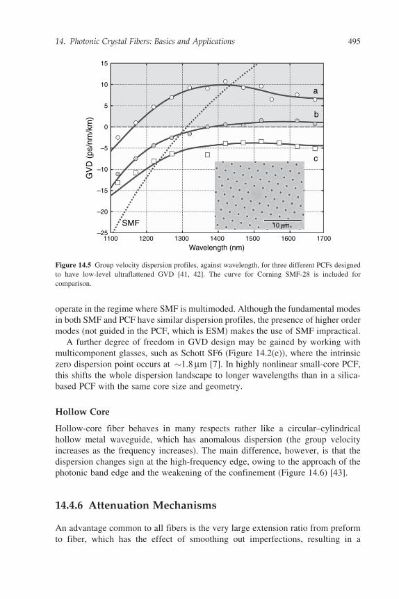
operate in the regime where SMF is multimoded. Although the fundamental modes
in both SMF and PCF have similar dispersion profiles, the presence of higher order
modes (not guided in the PCF, which is ESM) makes the use of SMF impractical.
A further degree of freedom in GVD design may be gained by working with
multicomponent glasses, such as Schott SF6 (Figure 14.2(e)), where the intrinsic
zero dispersion point occurs at �1.8 mm [7]. In highly nonlinear small-core PCF,
this shifts the whole dispersion landscape to longer wavelengths than in a silica-
based PCF with the same core size and geometry.
Hollow Core
Hollow-core fiber behaves in many respects rather like a circular–cylindrical
hollow metal waveguide, which has anomalous dispersion (the group velocity
increases as the frequency increases). The main difference, however, is that the
dispersion changes sign at the high-frequency edge, owing to the approach of the
photonic band edge and the weakening of the confinement (Figure 14.6) [43].
14.4.6 Attenuation Mechanisms
An advantage common to all fibers is the very large extension ratio from preform
to fiber, which has the effect of smoothing out imperfections, resulting in a
1100
SMF–25
–20
–15
–10
–5
0
5
10
15
1200 1300 1400
Wavelength (nm)
GV
D (
ps/n
m/k
m)
1500 1600
10 μm
c
b
a
1700
Figure 14.5 Group velocity dispersion profiles, against wavelength, for three different PCFs designed
to have low-level ultraflattened GVD [41, 42]. The curve for Corning SMF-28 is included for
comparison.
14. Photonic Crystal Fibers: Basics and Applications 495
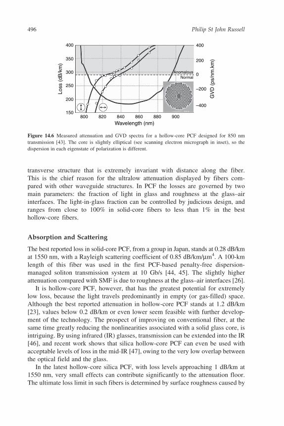
transverse structure that is extremely invariant with distance along the fiber.
This is the chief reason for the ultralow attenuation displayed by fibers com-
pared with other waveguide structures. In PCF the losses are governed by two
main parameters: the fraction of light in glass and roughness at the glass–air
interfaces. The light-in-glass fraction can be controlled by judicious design, and
ranges from close to 100% in solid-core fibers to less than 1% in the best
hollow-core fibers.
Absorption and Scattering
The best reported loss in solid-core PCF, from a group in Japan, stands at 0.28 dB/km
at 1550 nm, with a Rayleigh scattering coefficient of 0.85 dB/km/mm4. A 100-km
length of this fiber was used in the first PCF-based penalty-free dispersion-
managed soliton transmission system at 10 Gb/s [44, 45]. The slightly higher
attenuation compared with SMF is due to roughness at the glass–air interfaces [26].
It is hollow-core PCF, however, that has the greatest potential for extremely
low loss, because the light travels predominantly in empty (or gas-filled) space.
Although the best reported attenuation in hollow-core PCF stands at 1.2 dB/km
[23], values below 0.2 dB/km or even lower seem feasible with further develop-
ment of the technology. The prospect of improving on conventional fiber, at the
same time greatly reducing the nonlinearities associated with a solid glass core, is
intriguing. By using infrared (IR) glasses, transmission can be extended into the IR
[46], and recent work shows that silica hollow-core PCF can even be used with
acceptable levels of loss in the mid-IR [47], owing to the very low overlap between
the optical field and the glass.
In the latest hollow-core silica PCF, with loss levels approaching 1 dB/km at
1550 nm, very small effects can contribute significantly to the attenuation floor.
The ultimate loss limit in such fibers is determined by surface roughness caused by
800150
200
Loss
(dB
/km
)
250
300
350
400
820 840
Wavelength (nm)
GV
D (
ps/n
m.k
m)
860 880 900
AnomalousNormal
–400
–200
0
200
400
Figure 14.6 Measured attenuation and GVD spectra for a hollow-core PCF designed for 850 nm
transmission [43]. The core is slightly elliptical (see scanning electron micrograph in inset), so the
dispersion in each eigenstate of polarization is different.
496 Philip St John Russell
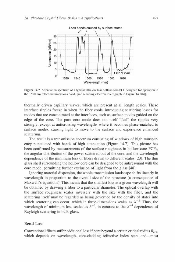
thermally driven capillary waves, which are present at all length scales. These
interface ripples freeze in when the fiber cools, introducing scattering losses for
modes that are concentrated at the interfaces, such as surface modes guided on the
edge of the core. The pure core mode does not itself “feel” the ripples very
strongly, except at anticrossing wavelengths where it becomes phase-matched to
surface modes, causing light to move to the surface and experience enhanced
scattering.
The result is a transmission spectrum consisting of windows of high transpar-
ency punctuated with bands of high attenuation (Figure 14.7). This picture has
been confirmed by measurements of the surface roughness in hollow-core PCFs,
the angular distribution of the power scattered out of the core, and the wavelength
dependence of the minimum loss of fibers drawn to different scales [23]. The thin
glass shell surrounding the hollow core can be designed to be antiresonant with the
core mode, permitting further exclusion of light from the glass [48].
Ignoring material dispersion, the whole transmission landscape shifts linearly in
wavelength in proportion to the overall size of the structure (a consequence of
Maxwell’s equations). This means that the smallest loss at a given wavelength will
be obtained by drawing a fiber to a particular diameter. The optical overlap with
the surface roughness scales inversely with the size with the fiber, and the
scattering itself may be regarded as being governed by the density of states into
which scattering can occur, which in three-dimensions scales as ��2. Thus, the
wavelength of minimum loss scales as ��3, in contrast to the ��4 dependence of
Rayleigh scattering in bulk glass.
Bend Loss
Conventional fibers suffer additional loss if bent beyond a certain critical radius Rcrit,
which depends on wavelength, core-cladding refractive index step, and—most
15200
5
10
15
20
25
30
1540 1560
Wavelength (nm)
Loss bands caused by surface states
Atte
nuat
ion
(dB
/km
)
1580 1600 1620
1.67 dB/km
Figure 14.7 Attenuation spectrum of a typical ultralow loss hollow-core PCF designed for operation in
the 1550 nm telecommunications band. [see scanning electron micrograph in Figure 14.2(h)].
14. Photonic Crystal Fibers: Basics and Applications 497
notably—the third power of core radius, a3 [49]. For wavelengths longer than a
certain value (the “long-wavelength bend edge”), all guidance is effectively lost.
A starting point for understanding bend loss in solid-core ESM-PCF (perhaps the
most interesting case) is the long-wavelength limit. ESM behavior occurs when
d/L< 0.43, which sets the highest air-filling fraction at 16.8% and yields an area-
averaged cladding refractive index of 1.388 (silica index of 1.444)—valid in the
limit k ! 0. This index step is some 10 times higher than in Corning SMF-28,
making ESM-PCF relatively much less susceptible to bend loss at long wavelengths.
For a step-index fiber with a Ge-doped core, 40 mol% of GeO2 would be needed to
reach the same index step (assuming 0.0014 index change per mol% GeO2 [50]).
The result is that the long-wavelength bend edge in ESM-PCF is in the (IR) beyond
the transparency window of silica glass, even when the core radius is large [51].
ESM-PCF also exhibits a short-wavelength bend edge, caused by bend-induced
coupling from the fundamental to higher order modes, which of course leak out of
the core [14]. The critical bend radius for this loss varies as:
Rc e�3=�2 (14.4)
compared with Rc�� for SMF. The reciprocal dependence on �2 makes it inevi-
table that a short-wavelength bend edge will appear in ESM-PCF. It turns out that a
step-index fiber with core-cladding index difference D1 (i.e., the value for an
ESM-PCF in the long-wavelength limit) is multimode over wide parameter ranges
where ESM-PCF has negligible bend loss.
In contrast, hollow-core PCF is experimentally very insensitive to bend loss—
in many cases no appreciable drop in transmission is observed until the fiber
breaks. This is because the effective depth of “potential well” for the guided
light (see Section “Hollow-Core Silica/Air”), given by the distance D� between
the edges of the PBG, is substantially larger than in SMF.
Confinement Loss
The photonic crystal cladding in a realistic PCF is of course finite in extent. For a
guided mode, the Bloch waves in the cladding are evanescent, just like the evanes-
cent plane waves in the cladding of a conventional fiber. If the cladding is not thick
enough, the evanescent field amplitudes at the cladding/coating boundary can be
substantial, causing attenuation. In the solid-core case for small values of d/L, the
resulting loss can be large unless a sufficiently large number of periods is used [41].
Very similar losses are observed in hollow-core fibers, where the “strength” of
the PBG (closely related to its width in �) determines how many periods are
needed to reduce confinement loss to acceptable levels. Numerical modeling is
useful for giving an indication of how many periods are needed to reach a required
loss level. The cladding field intensity in the ultralow loss PCF reported in Ref.
[23] falls by �9 dB per period, reaching �63 dB at the edge of the photonic
crystal region.
498 Philip St John Russell
14.4.7 Kerr Nonlinearities
The ability to enhance or reduce the effective Kerr nonlinearity, and at the same
time control the magnitude and wavelength dependence of the GVD, makes PCF a
versatile vehicle for studies of effects such as four-wave mixing, self-phase
modulation, modulation instability, soliton formation, and stimulated Raman scat-
tering (SRS). For a composite PCF made from two or more homogeneous materials,
the � coefficient of fiber nonlinearity takes the form [52]
� = kX
i
ni2
Ai
(14.5)
where n2i is the nonlinear refractive index of material i and Ai its nonlinear
effective area:
Ai =nm
ÐÐ 2ðx; yÞ dxdy
� �2ÐÐuiðx; yÞ 4ðx; yÞ dxdy
(14.6)
where ui(x, y) equals ni in regions made from material i and zero elsewhere. In this
expression, nm is the guided mode phase index and c(x, y) is the scalar transverse
field amplitude profile.
In air, the nonlinear refractive index is 2.9� 10�23 m2/W1, in silica it is
2.5� 10�20 m2/W1, and in multicomponent glasses it can be an order of magnitude
or more higher. The highest nonlinearity available in conventional step-index
fibers is � ’ 20 W/km1 at 1550 nm [53]. By comparison, a solid-core PCF similar
to the one in Figure 14.1(f) but with a core diameter 1 mm has a nonlinearity of
� ’ 240 W1/km1 at 850 nm, and values as high as �= 550 W/km1 at 1550 nm
have been measured for PCFs made from multicomponent glasses [54]. In
complete contrast, hollow-core PCF has extremely low levels of nonlinearity,
owing to the small overlap between the glass and the light. In a recent example,
a fiber was reported with a nonlinear coefficient �= 0.023 W/km1 (some� 104
smaller than in a typical highly nonlinear solid-core PCF) [55, 56].
Although the level of nonlinearity is clearly important, the actual nonlinear
effects that appear in a particular case are also strongly dependent on the magni-
tude, sign, and wavelength dependence of the GVD (see Section 14.6.3) as well as
on the characteristics of the laser pulses [57].
14.5 INTRA-FIBER DEVICES, CUTTING AND JOINING
As PCF becomes more widely used, there is an increasing need for effective
cleaves, low-loss splices, multiport couplers, intra-fiber devices, and mode-area
transformers. The airholes provide an opportunity not available in standard
14. Photonic Crystal Fibers: Basics and Applications 499
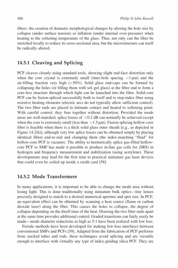
fibers: the creation of dramatic morphological changes by altering the hole size by
collapse (under surface tension) or inflation (under internal over-pressure) when
heating to the softening temperature of the glass. Thus, not only can the fiber be
stretched locally to reduce its cross-sectional area, but the microstructure can itself
be radically altered.
14.5.1 Cleaving and Splicing
PCF cleaves cleanly using standard tools, showing slight end-face distortion only
when the core crystal is extremely small (inter-hole spacing �1 mm) and the
air-filling fraction very high (>50%). Solid glass end-caps can be formed by
collapsing the holes (or filling them with sol–gel glass) at the fiber end to form a
core-less structure through which light can be launched into the fiber. Solid-core
PCF can be fusion-spliced successfully both to itself and to step-index fiber using
resistive heating elements (electric arcs do not typically allow sufficient control).
The two fiber ends are placed in intimate contact and heated to softening point.
With careful control, they fuse together without distortion. Provided the mode
areas are well-matched, splice losses of <0.2 dB can normally be achieved except
when the core is extremely small (less than �1.5 mm). Fusion splicing hollow-core
fiber is feasible when there is a thick solid glass outer sheath [e.g., as depicted in
Figure 14.2(h)], although very low splice losses can be obtained simply by placing
identical fibers end-to-end and clamping them (the index-matching “fluid” for
hollow-core PCF is vacuum). The ability to hermetically splice gas-filled hollow-
core PCF to SMF has made it possible to produce in-line gas cells for (SRS) in
hydrogen and frequency measurement and stabilization (using acetylene). These
developments may lead for the first time to practical miniature gas laser devices
that could even be coiled up inside a credit card [58].
14.5.2 Mode Transformers
In many applications, it is important to be able to change the mode area without
losing light. This is done traditionally using miniature bulk optics—tiny lenses
precisely designed to match to a desired numerical aperture and spot size. In PCF,
an equivalent effect can be obtained by scanning a heat source (flame or carbon
dioxide laser) along the fiber. This causes the holes to collapse, the degree of
collapse depending on the dwell time of the heat. Drawing the two fiber ends apart
at the same time provides additional control. Graded transitions can fairly easily be
made—mode diameter reductions as high as 5:1 have been realized with low loss.
Ferrule methods have been developed for making low-loss interfaces between
conventional SMFs and PCFs [59]. Adapted from the fabrication of PCF preforms
from stacked tubes and rods, these techniques avoid splicing and are versatile
enough to interface with virtually any type of index-guiding silica PCF. They are
500 Philip St John Russell
effective for coupling light into and out of all the individual cores of a multicore
fiber without input or output crosstalk. The technique also creates another oppor-
tunity—the use of taper transitions to couple light between a multimode fiber and
several SMFs. When the number of SMFs matches the number of spatial modes in
the multimode fiber, the transition can have low loss in both directions. This means
that the high performance of SMF devices can be reached in multimode systems,
for example, a multimode fiber filter with the transmission spectrum of a SMF
Bragg grating [60], a device that has applications in earth-based astronomy, where
the high throughput of a multimode fiber can be retained while unwanted atmo-
spheric emission lines are filtered out.
A further degree of freedom may be gained by pressurizing the holes during the
taper process [61]. The resulting hole inflation permits radical changes in the
guidance characteristics. It is possible, for example, to transform a PCF, with a
relatively large core and small air-filling fraction, into a PCF with a very small
core and a large air-filling fraction, the transitions having very low loss [62].
14.5.3 In-Fiber Devices
Precise use of heat and pressure induces large changes in the optical character-
istics of PCF, giving rise to a whole family of new intra-fiber components.
Micro-couplers can be made in a PCF with two optically isolated cores by
collapsing the holes so as to allow the mode fields to expand and interact with
each other, creating local coupling [63]. Long-period gratings, which scatter the
core light into cladding modes within certain wavelength bands, can be made by
periodic modulation of hole size [64]. By rocking a birefringent PCF to and fro,
while scanning a carbon dioxide laser along it, so-called rocking filters can be
made, which transfer power from one polarization state to the other within a
narrow band of wavelengths [65]. All these components have one great advan-
tage over equivalent devices made in conventional fiber: being formed by
permanent changes in morphology, they are highly stable with temperature and
over time.
Heating and stretching PCF can result in quite remarkable changes in the scale
of the micro/nanostructures, without significant distortion. Recently, a solid-core
PCF was reduced five times in linear scale, resulting in a core diameter of 500 nm
(Figure 14.8). This permitted formation of a PCF with a zero dispersion wave-
length that matched the 532 nm emission wavelength of a frequency-doubled
Nd:YAG laser [66] (this is important for supercontinuum (SC) generation—see
Section Supercontinuum Generation). A further compelling advantage of the
tapering approach is that it neatly sidesteps the difficulty of launching light into
submicron-sized cores; light is launched into the entry port (in this case with core
diameter 2.5 mm) and adiabatically evolves, with negligible loss, into the mode of
the 500 nm core.
14. Photonic Crystal Fibers: Basics and Applications 501
14.6 APPLICATIONS
The diversity of new or improved features, beyond conventional fibers, means that
PCFs are finding an increasing number of applications in every widening area of
science and technology.
14.6.1 High Power and Energy Transmission
Larger mode areas allow higher power to be carried before the onset of intensity-
related nonlinearities or damage, with obvious benefits for delivery of high laser
power, and for high-power fiber amplifiers and lasers. ESM-PCF’s ability to
remain single mode at all wavelengths where it guides, and for all scales of
structure, means that the core area can be increased without the penalty of
introducing higher order guided modes [19]. This also suggests that it should
have superior power-handling properties, with applications in, for example, the
field of laser machining. A key issue is bend loss, and as we have seen, it turns out
that PCF offers a wider bandwidth of useful single-mode guidance than high-delta
SMF, because it can operate in the multimode regime of SMF while remaining
single mode (Section “Bend Loss”). This also shifts the long wavelength bend-
edge to longer wavelengths than is possible in standard fibers.
Hollow-core PCF is also an excellent candidate for transmitting high contin-
uous-wave power as well as ultrashort pulses with very high peak powers. Solitons
have been reported at 800 nm using a Ti:sapphire laser [55] and at 1550 nm with
durations of 100 fs and peak powers of 2 MW [67]. The soliton energy is of course
determined by the effective value of � (Section 14.4.7) and the magnitude of the
anomalous GVD. As mentioned in Section “Hollow Core,” the GVD changes sign
Figure 14.8 Scanning electron micrographs (depicted to the same scale) of the fiber cross sections
produced by tapering a solid-core PCF. The structures are well preserved, even down to core diameters
of 500 nm [66].
502 Philip St John Russell
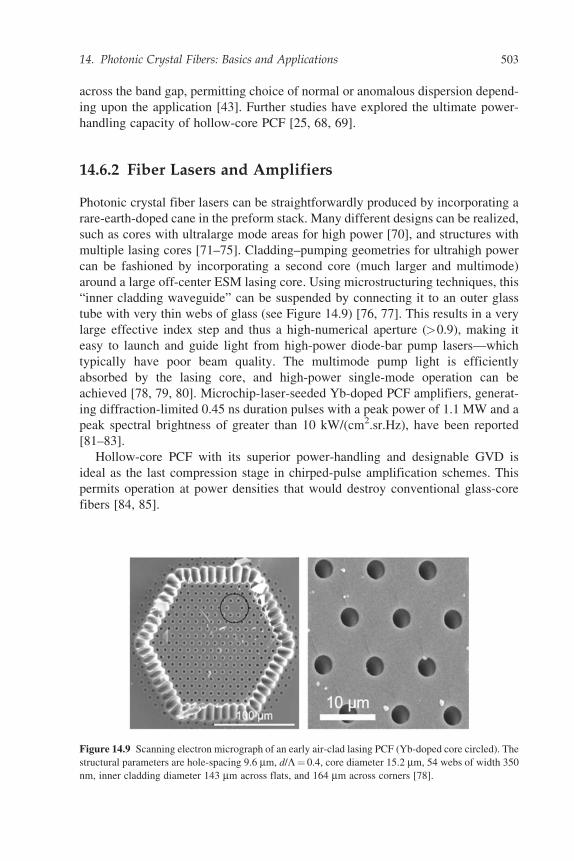
across the band gap, permitting choice of normal or anomalous dispersion depend-
ing upon the application [43]. Further studies have explored the ultimate power-
handling capacity of hollow-core PCF [25, 68, 69].
14.6.2 Fiber Lasers and Amplifiers
Photonic crystal fiber lasers can be straightforwardly produced by incorporating a
rare-earth-doped cane in the preform stack. Many different designs can be realized,
such as cores with ultralarge mode areas for high power [70], and structures with
multiple lasing cores [71–75]. Cladding–pumping geometries for ultrahigh power
can be fashioned by incorporating a second core (much larger and multimode)
around a large off-center ESM lasing core. Using microstructuring techniques, this
“inner cladding waveguide” can be suspended by connecting it to an outer glass
tube with very thin webs of glass (see Figure 14.9) [76, 77]. This results in a very
large effective index step and thus a high-numerical aperture (>0.9), making it
easy to launch and guide light from high-power diode-bar pump lasers—which
typically have poor beam quality. The multimode pump light is efficiently
absorbed by the lasing core, and high-power single-mode operation can be
achieved [78, 79, 80]. Microchip-laser-seeded Yb-doped PCF amplifiers, generat-
ing diffraction-limited 0.45 ns duration pulses with a peak power of 1.1 MW and a
peak spectral brightness of greater than 10 kW/(cm2.sr.Hz), have been reported
[81–83].
Hollow-core PCF with its superior power-handling and designable GVD is
ideal as the last compression stage in chirped-pulse amplification schemes. This
permits operation at power densities that would destroy conventional glass-core
fibers [84, 85].
Figure 14.9 Scanning electron micrograph of an early air-clad lasing PCF (Yb-doped core circled). The
structural parameters are hole-spacing 9.6 mm, d/L= 0.4, core diameter 15.2 mm, 54 webs of width 350
nm, inner cladding diameter 143 mm across flats, and 164 mm across corners [78].
14. Photonic Crystal Fibers: Basics and Applications 503
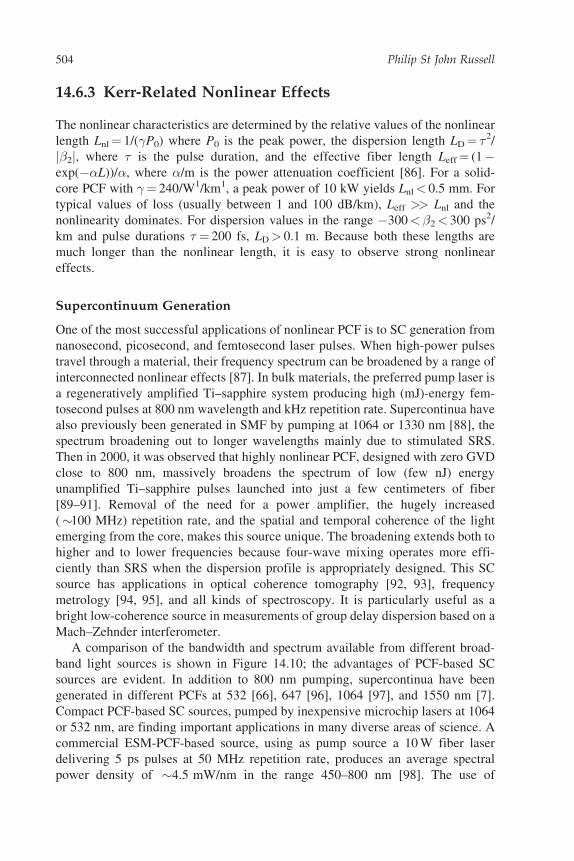
14.6.3 Kerr-Related Nonlinear Effects
The nonlinear characteristics are determined by the relative values of the nonlinear
length Lnl = 1/(�P0) where P0 is the peak power, the dispersion length LD = �2/
j�2j, where � is the pulse duration, and the effective fiber length Leff = (1�exp(��L))/�, where �/m is the power attenuation coefficient [86]. For a solid-
core PCF with �= 240/W1/km1, a peak power of 10 kW yields Lnl< 0.5 mm. For
typical values of loss (usually between 1 and 100 dB/km), Leff >> Lnl and the
nonlinearity dominates. For dispersion values in the range �300<�2< 300 ps2/
km and pulse durations � = 200 fs, LD> 0.1 m. Because both these lengths are
much longer than the nonlinear length, it is easy to observe strong nonlinear
effects.
Supercontinuum Generation
One of the most successful applications of nonlinear PCF is to SC generation from
nanosecond, picosecond, and femtosecond laser pulses. When high-power pulses
travel through a material, their frequency spectrum can be broadened by a range of
interconnected nonlinear effects [87]. In bulk materials, the preferred pump laser is
a regeneratively amplified Ti–sapphire system producing high (mJ)-energy fem-
tosecond pulses at 800 nm wavelength and kHz repetition rate. Supercontinua have
also previously been generated in SMF by pumping at 1064 or 1330 nm [88], the
spectrum broadening out to longer wavelengths mainly due to stimulated SRS.
Then in 2000, it was observed that highly nonlinear PCF, designed with zero GVD
close to 800 nm, massively broadens the spectrum of low (few nJ) energy
unamplified Ti–sapphire pulses launched into just a few centimeters of fiber
[89–91]. Removal of the need for a power amplifier, the hugely increased
(�100 MHz) repetition rate, and the spatial and temporal coherence of the light
emerging from the core, makes this source unique. The broadening extends both to
higher and to lower frequencies because four-wave mixing operates more effi-
ciently than SRS when the dispersion profile is appropriately designed. This SC
source has applications in optical coherence tomography [92, 93], frequency
metrology [94, 95], and all kinds of spectroscopy. It is particularly useful as a
bright low-coherence source in measurements of group delay dispersion based on a
Mach–Zehnder interferometer.
A comparison of the bandwidth and spectrum available from different broad-
band light sources is shown in Figure 14.10; the advantages of PCF-based SC
sources are evident. In addition to 800 nm pumping, supercontinua have been
generated in different PCFs at 532 [66], 647 [96], 1064 [97], and 1550 nm [7].
Compact PCF-based SC sources, pumped by inexpensive microchip lasers at 1064
or 532 nm, are finding important applications in many diverse areas of science. A
commercial ESM-PCF-based source, using as pump source a 10 W fiber laser
delivering 5 ps pulses at 50 MHz repetition rate, produces an average spectral
power density of �4.5 mW/nm in the range 450–800 nm [98]. The use of
504 Philip St John Russell
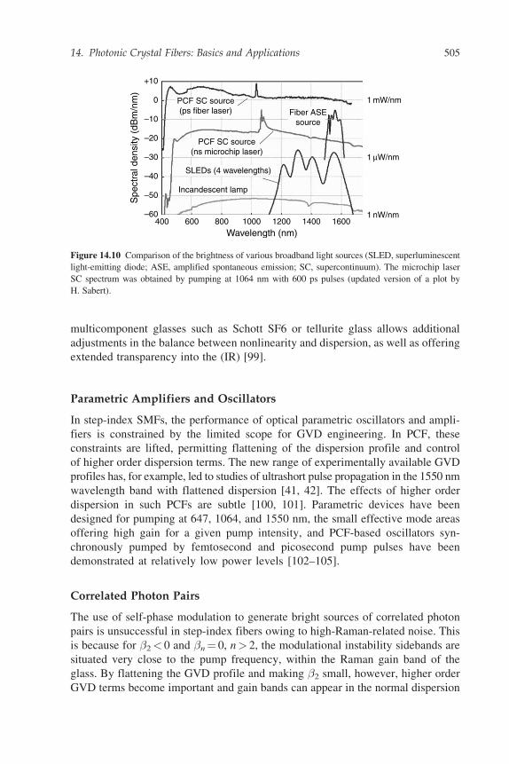
multicomponent glasses such as Schott SF6 or tellurite glass allows additional
adjustments in the balance between nonlinearity and dispersion, as well as offering
extended transparency into the (IR) [99].
Parametric Amplifiers and Oscillators
In step-index SMFs, the performance of optical parametric oscillators and ampli-
fiers is constrained by the limited scope for GVD engineering. In PCF, these
constraints are lifted, permitting flattening of the dispersion profile and control
of higher order dispersion terms. The new range of experimentally available GVD
profiles has, for example, led to studies of ultrashort pulse propagation in the 1550 nm
wavelength band with flattened dispersion [41, 42]. The effects of higher order
dispersion in such PCFs are subtle [100, 101]. Parametric devices have been
designed for pumping at 647, 1064, and 1550 nm, the small effective mode areas
offering high gain for a given pump intensity, and PCF-based oscillators syn-
chronously pumped by femtosecond and picosecond pump pulses have been
demonstrated at relatively low power levels [102–105].
Correlated Photon Pairs
The use of self-phase modulation to generate bright sources of correlated photon
pairs is unsuccessful in step-index fibers owing to high-Raman-related noise. This
is because for �2< 0 and �n = 0, n> 2, the modulational instability sidebands are
situated very close to the pump frequency, within the Raman gain band of the
glass. By flattening the GVD profile and making �2 small, however, higher order
GVD terms become important and gain bands can appear in the normal dispersion
400–60
–50
–40
–30
–20
–10
0
+10
600
Incandescent lamp
SLEDs (4 wavelengths)
PCF SC source(ns microchip laser)
PCF SC source(ps fiber laser) Fiber ASE
source
800 1000Wavelength (nm)
Spe
ctra
l den
sity
(dB
m/n
m)
1200 1400 16001 nW/nm
1 μW/nm
1 mW/nm
Figure 14.10 Comparison of the brightness of various broadband light sources (SLED, superluminescent
light-emitting diode; ASE, amplified spontaneous emission; SC, supercontinuum). The microchip laser
SC spectrum was obtained by pumping at 1064 nm with 600 ps pulses (updated version of a plot by
H. Sabert).
14. Photonic Crystal Fibers: Basics and Applications 505
regime for �2> 0 and �4< 0 [42]. The relevant expression for the sideband gain
(m�1), including �4 and �6, is
gain= ImffiffiffiffiffiffiffiffiffiffiffiffiffiffiffiffiffiffiffiffiffiffiffiffiffiQ Qþ 2�Pð Þ
ph i
Q = �2�2=2þ �4�4=24þ �6�6=720
(14.7)
where � is the nonlinear coefficient (Eqn (14.5)), P the pump power, and � the
angular frequency offset from the pump frequency. This expression may be
used to show that the sidebands can be widely spaced from the pump frequency,
their position and width being controllable by engineering the even-order
higher order dispersion terms (Figure 14.11). It is straightforward to arrange
that these sidebands lie well beyond the Raman gain band, reducing the Raman
noise and allowing PCF to be used as a compact, bright, tunable, single-mode
source of pair-photons with wide applications in quantum communications
[106, 107].
In a recent example, a PCF with zero dispersion at 715 nm was pumped by a
Ti:sapphire laser at 708 nm (normal dispersion) [108]. Under these conditions,
phase-matching is satisfied by signal and idler waves at 587 and 897 nm, and 10
million photon pairs per second were generated and delivered through single-mode
fiber to Si avalanche detectors, producing �3.2� 105 coincidences per second for
a pump power of 0.5 mW. These results point the way to practical and efficient
sources of entangled photon pairs that can be used as building blocks in future
multiphoton interference experiments.
More complicated and potentially engineerable effects can be obtained by
adding one or more pump lasers at different frequencies; this has the effect of
altering the MI gain spectrum.
0
a
Anomalous
Normal
b c–0.10
–0.05
0
0.05
0
Frequency (ω – ωo)
Dis
pers
ion
β 2
0
Figure 14.11 Density plots of the level of modulational instability gain as a function of frequency
offset from a strong single-frequency pump laser and the level of �2 at the pump frequency. The black to
white regions represent gain on a linear scale of grey; gain is zero in the black regions. The nonlinear
length Lnl = 1/(�P0) is 0.1 in each case (see Section 14.6.3): (a) �4 = 0, �2 = 0; (b) �4 =�10�3, �2 = 0;
(c) �4 =�10�3, �2 = 1.24 � 10�5. The units in each case are psn/km for �n.
506 Philip St John Russell
Soliton Self-Frequency Shift Cancellation
The ability to create PCFs with negative dispersion slope at the zero dispersion
wavelength (in SMF the slope is positive, i.e., the dispersion becomes more anom-
alous as the wavelength increases) has made it possible to observe Cerenkov-like
effects in which solitons (which form on the anomalous side of the dispersion zero)
shed power into dispersive radiation at longer wavelengths on the normal side of the
dispersion zero. This occurs because higher order dispersion causes the edges of
the soliton spectrum to phase-match to linear waves. The result is stabilization of the
soliton self-frequency shift, at the cost of gradual loss of soliton energy [109].
The behavior of solitons in the presence of wavelength-dependent dispersion is the
subject of many recent studies, for example, Ref. [110]. Interactions between
solitons have also been studied in a number of recent papers [111, 112].
14.6.4 Brillouin Scattering
The periodic micro/nanostructuring in ultrasmall core glass–air PCF strongly alters
the acoustic properties compared with that in conventional SMF [113–116]. Sound
can be guided in the core both as leaky and as tightly confined acoustic modes. In
addition, the complex geometry and “hard” boundaries cause coupling between all
three displacement components (radial, azimuthal, and axial), with the result that
each acoustic mode has elements of both shear and longitudinal strain. This
complex acoustic behavior strongly alters the characteristics of both forward and
backward Brillouin scattering.
Backward Scattering
When a solid-core silica–air PCF has a core diameter of around 70% of the
vacuum wavelength of the launched laser light, and the air-filling fraction in the
cladding is very high, the spontaneous Brillouin signal displays multiple bands
with Stokes frequency shifts in the 10 GHz range. These peaks are caused by
discrete guided acoustic modes, each with different proportions of longitudinal and
shear strain, strongly localized to the core [117]. At the same time, the threshold
power for stimulated Brillouin scattering increases fivefold—a rather unexpected
result, because conventionally one would assume that higher intensities yield
lower nonlinear threshold powers. This occurs because the effective overlap
between the tightly confined acoustic modes and the optical mode is actually
smaller than in a conventional fiber core; the sound field contains a large propor-
tion of shear strain, which does not contribute significantly to changes in refractive
index. This is of direct practical relevance to parametric amplifiers (Section
“Parametric Amplifiers and Oscillators”), which can be pumped five times harder
before stimulated Brillouin scattering appears.
14. Photonic Crystal Fibers: Basics and Applications 507
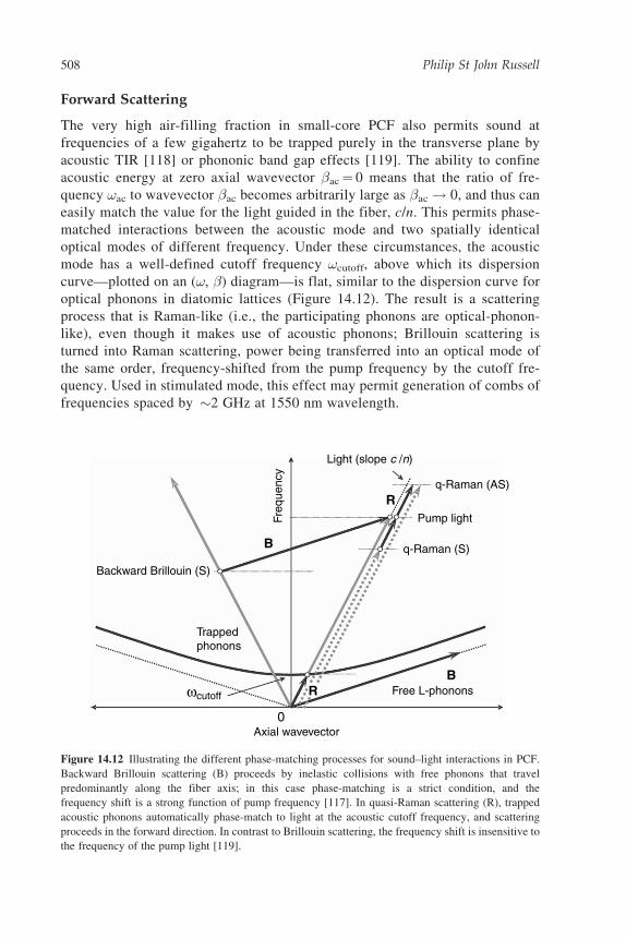
Forward Scattering
The very high air-filling fraction in small-core PCF also permits sound at
frequencies of a few gigahertz to be trapped purely in the transverse plane by
acoustic TIR [118] or phononic band gap effects [119]. The ability to confine
acoustic energy at zero axial wavevector �ac = 0 means that the ratio of fre-
quency !ac to wavevector �ac becomes arbitrarily large as �ac! 0, and thus can
easily match the value for the light guided in the fiber, c/n. This permits phase-
matched interactions between the acoustic mode and two spatially identical
optical modes of different frequency. Under these circumstances, the acoustic
mode has a well-defined cutoff frequency !cutoff, above which its dispersion
curve—plotted on an (!, �) diagram—is flat, similar to the dispersion curve for
optical phonons in diatomic lattices (Figure 14.12). The result is a scattering
process that is Raman-like (i.e., the participating phonons are optical-phonon-
like), even though it makes use of acoustic phonons; Brillouin scattering is
turned into Raman scattering, power being transferred into an optical mode of
the same order, frequency-shifted from the pump frequency by the cutoff fre-
quency. Used in stimulated mode, this effect may permit generation of combs of
frequencies spaced by �2 GHz at 1550 nm wavelength.
0Axial wavevector
R
R
B
B
Trappedphonons
Backward Brillouin (S)
ωcutoff Free L-phonons
q-Raman (S)
q-Raman (AS)
Light (slope c /n)
Freq
uenc
y
Pump light
Figure 14.12 Illustrating the different phase-matching processes for sound–light interactions in PCF.
Backward Brillouin scattering (B) proceeds by inelastic collisions with free phonons that travel
predominantly along the fiber axis; in this case phase-matching is a strict condition, and the
frequency shift is a strong function of pump frequency [117]. In quasi-Raman scattering (R), trapped
acoustic phonons automatically phase-match to light at the acoustic cutoff frequency, and scattering
proceeds in the forward direction. In contrast to Brillouin scattering, the frequency shift is insensitive to
the frequency of the pump light [119].
508 Philip St John Russell
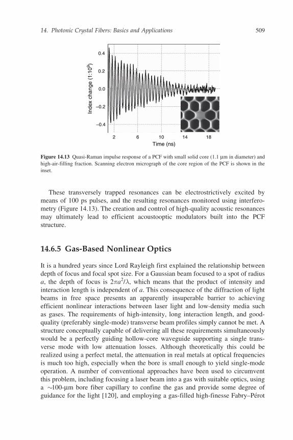
These transversely trapped resonances can be electrostrictively excited by
means of 100 ps pulses, and the resulting resonances monitored using interfero-
metry (Figure 14.13). The creation and control of high-quality acoustic resonances
may ultimately lead to efficient acoustooptic modulators built into the PCF
structure.
14.6.5 Gas-Based Nonlinear Optics
It is a hundred years since Lord Rayleigh first explained the relationship between
depth of focus and focal spot size. For a Gaussian beam focused to a spot of radius
a, the depth of focus is 2�a2/�, which means that the product of intensity and
interaction length is independent of a. This consequence of the diffraction of light
beams in free space presents an apparently insuperable barrier to achieving
efficient nonlinear interactions between laser light and low-density media such
as gases. The requirements of high-intensity, long interaction length, and good-
quality (preferably single-mode) transverse beam profiles simply cannot be met. A
structure conceptually capable of delivering all these requirements simultaneously
would be a perfectly guiding hollow-core waveguide supporting a single trans-
verse mode with low attenuation losses. Although theoretically this could be
realized using a perfect metal, the attenuation in real metals at optical frequencies
is much too high, especially when the bore is small enough to yield single-mode
operation. A number of conventional approaches have been used to circumvent
this problem, including focusing a laser beam into a gas with suitable optics, using
a �100-mm bore fiber capillary to confine the gas and provide some degree of
guidance for the light [120], and employing a gas-filled high-finesse Fabry–Perot
2
–0.4
–0.2
0.0
0.2
0.4
6 10
Time (ns)
Inde
x ch
ange
(1:
109 )
14 18
Figure 14.13 Quasi-Raman impulse response of a PCF with small solid core (1.1 mm in diameter) and
high-air-filling fraction. Scanning electron micrograph of the core region of the PCF is shown in the
inset.
14. Photonic Crystal Fibers: Basics and Applications 509
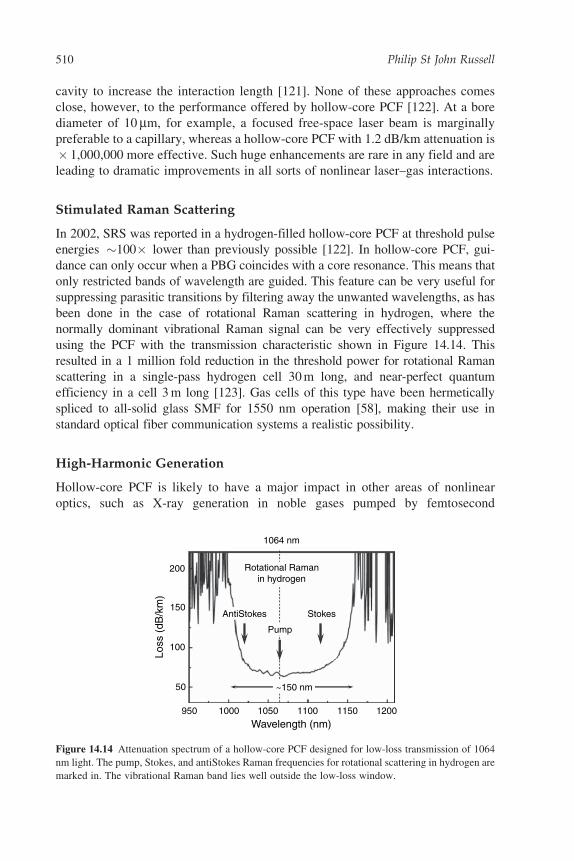
cavity to increase the interaction length [121]. None of these approaches comes
close, however, to the performance offered by hollow-core PCF [122]. At a bore
diameter of 10 mm, for example, a focused free-space laser beam is marginally
preferable to a capillary, whereas a hollow-core PCF with 1.2 dB/km attenuation is
� 1,000,000 more effective. Such huge enhancements are rare in any field and are
leading to dramatic improvements in all sorts of nonlinear laser–gas interactions.
Stimulated Raman Scattering
In 2002, SRS was reported in a hydrogen-filled hollow-core PCF at threshold pulse
energies �100� lower than previously possible [122]. In hollow-core PCF, gui-
dance can only occur when a PBG coincides with a core resonance. This means that
only restricted bands of wavelength are guided. This feature can be very useful for
suppressing parasitic transitions by filtering away the unwanted wavelengths, as has
been done in the case of rotational Raman scattering in hydrogen, where the
normally dominant vibrational Raman signal can be very effectively suppressed
using the PCF with the transmission characteristic shown in Figure 14.14. This
resulted in a 1 million fold reduction in the threshold power for rotational Raman
scattering in a single-pass hydrogen cell 30 m long, and near-perfect quantum
efficiency in a cell 3 m long [123]. Gas cells of this type have been hermetically
spliced to all-solid glass SMF for 1550 nm operation [58], making their use in
standard optical fiber communication systems a realistic possibility.
High-Harmonic Generation
Hollow-core PCF is likely to have a major impact in other areas of nonlinear
optics, such as X-ray generation in noble gases pumped by femtosecond
950
50
100
150
200
1000 1050
~150 nm
Pump
StokesAntiStokes
Rotational Ramanin hydrogen
1064 nm
Wavelength (nm)
Loss
(dB
/km
)
1100 1150 1200
Figure 14.14 Attenuation spectrum of a hollow-core PCF designed for low-loss transmission of 1064
nm light. The pump, Stokes, and antiStokes Raman frequencies for rotational scattering in hydrogen are
marked in. The vibrational Raman band lies well outside the low-loss window.
510 Philip St John Russell
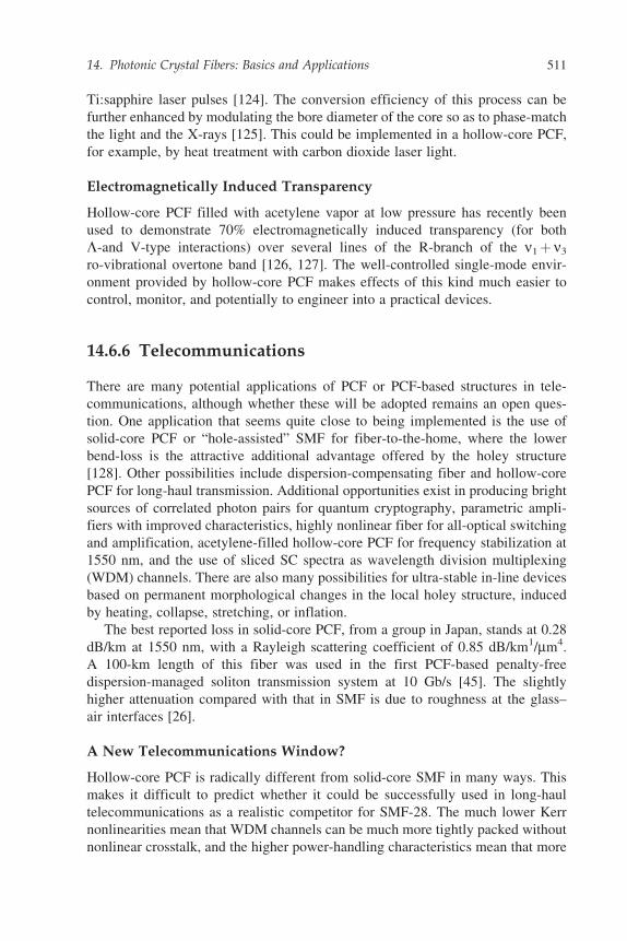
Ti:sapphire laser pulses [124]. The conversion efficiency of this process can be
further enhanced by modulating the bore diameter of the core so as to phase-match
the light and the X-rays [125]. This could be implemented in a hollow-core PCF,
for example, by heat treatment with carbon dioxide laser light.
Electromagnetically Induced Transparency
Hollow-core PCF filled with acetylene vapor at low pressure has recently been
used to demonstrate 70% electromagnetically induced transparency (for both
L-and V-type interactions) over several lines of the R-branch of the n1þ n3
ro-vibrational overtone band [126, 127]. The well-controlled single-mode envir-
onment provided by hollow-core PCF makes effects of this kind much easier to
control, monitor, and potentially to engineer into a practical devices.
14.6.6 Telecommunications
There are many potential applications of PCF or PCF-based structures in tele-
communications, although whether these will be adopted remains an open ques-
tion. One application that seems quite close to being implemented is the use of
solid-core PCF or “hole-assisted” SMF for fiber-to-the-home, where the lower
bend-loss is the attractive additional advantage offered by the holey structure
[128]. Other possibilities include dispersion-compensating fiber and hollow-core
PCF for long-haul transmission. Additional opportunities exist in producing bright
sources of correlated photon pairs for quantum cryptography, parametric ampli-
fiers with improved characteristics, highly nonlinear fiber for all-optical switching
and amplification, acetylene-filled hollow-core PCF for frequency stabilization at
1550 nm, and the use of sliced SC spectra as wavelength division multiplexing
(WDM) channels. There are also many possibilities for ultra-stable in-line devices
based on permanent morphological changes in the local holey structure, induced
by heating, collapse, stretching, or inflation.
The best reported loss in solid-core PCF, from a group in Japan, stands at 0.28
dB/km at 1550 nm, with a Rayleigh scattering coefficient of 0.85 dB/km1/mm4.
A 100-km length of this fiber was used in the first PCF-based penalty-free
dispersion-managed soliton transmission system at 10 Gb/s [45]. The slightly
higher attenuation compared with that in SMF is due to roughness at the glass–
air interfaces [26].
A New Telecommunications Window?
Hollow-core PCF is radically different from solid-core SMF in many ways. This
makes it difficult to predict whether it could be successfully used in long-haul
telecommunications as a realistic competitor for SMF-28. The much lower Kerr
nonlinearities mean that WDM channels can be much more tightly packed without
nonlinear crosstalk, and the higher power-handling characteristics mean that more
14. Photonic Crystal Fibers: Basics and Applications 511
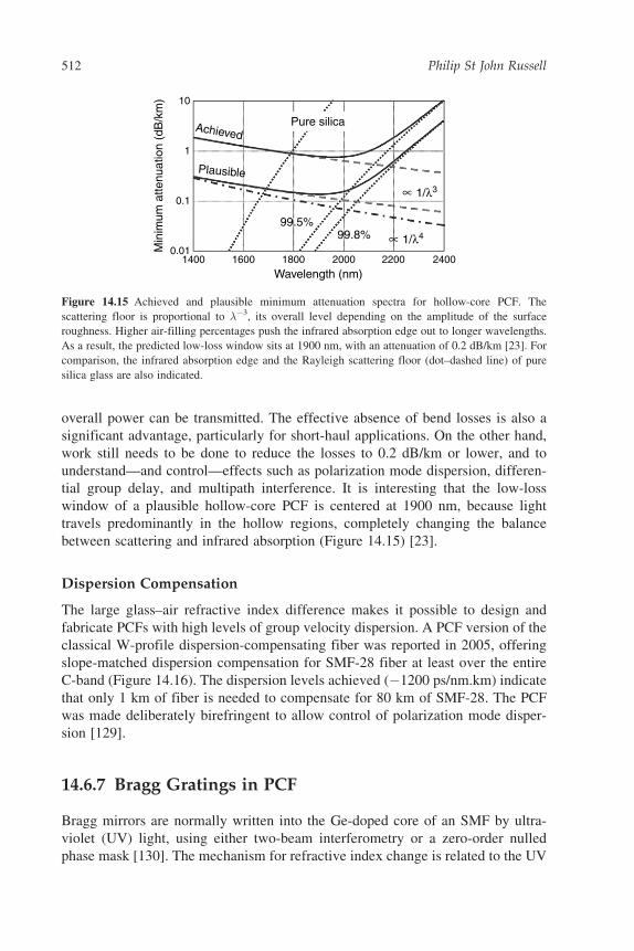
overall power can be transmitted. The effective absence of bend losses is also a
significant advantage, particularly for short-haul applications. On the other hand,
work still needs to be done to reduce the losses to 0.2 dB/km or lower, and to
understand—and control—effects such as polarization mode dispersion, differen-
tial group delay, and multipath interference. It is interesting that the low-loss
window of a plausible hollow-core PCF is centered at 1900 nm, because light
travels predominantly in the hollow regions, completely changing the balance
between scattering and infrared absorption (Figure 14.15) [23].
Dispersion Compensation
The large glass–air refractive index difference makes it possible to design and
fabricate PCFs with high levels of group velocity dispersion. A PCF version of the
classical W-profile dispersion-compensating fiber was reported in 2005, offering
slope-matched dispersion compensation for SMF-28 fiber at least over the entire
C-band (Figure 14.16). The dispersion levels achieved (�1200 ps/nm.km) indicate
that only 1 km of fiber is needed to compensate for 80 km of SMF-28. The PCF
was made deliberately birefringent to allow control of polarization mode disper-
sion [129].
14.6.7 Bragg Gratings in PCF
Bragg mirrors are normally written into the Ge-doped core of an SMF by ultra-
violet (UV) light, using either two-beam interferometry or a zero-order nulled
phase mask [130]. The mechanism for refractive index change is related to the UV
14000.01
0.1
1
10
1600
Plausible
Achieved
1800
Wavelength (nm)
99.5%99.8%
∝ 1/λ3
∝ 1/λ4
Pure silica
Min
imum
atte
nuat
ion
(dB
/km
)
2000 2200 2400
Figure 14.15 Achieved and plausible minimum attenuation spectra for hollow-core PCF. The
scattering floor is proportional to ��3, its overall level depending on the amplitude of the surface
roughness. Higher air-filling percentages push the infrared absorption edge out to longer wavelengths.
As a result, the predicted low-loss window sits at 1900 nm, with an attenuation of 0.2 dB/km [23]. For
comparison, the infrared absorption edge and the Rayleigh scattering floor (dot–dashed line) of pure
silica glass are also indicated.
512 Philip St John Russell
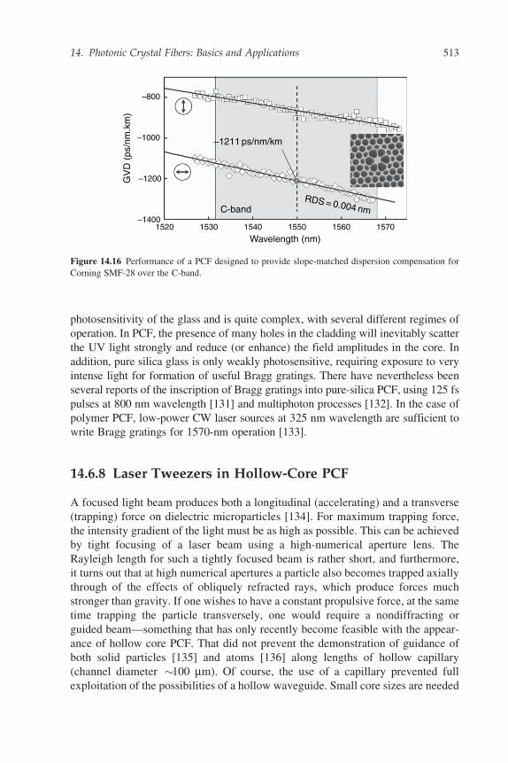
photosensitivity of the glass and is quite complex, with several different regimes of
operation. In PCF, the presence of many holes in the cladding will inevitably scatter
the UV light strongly and reduce (or enhance) the field amplitudes in the core. In
addition, pure silica glass is only weakly photosensitive, requiring exposure to very
intense light for formation of useful Bragg gratings. There have nevertheless been
several reports of the inscription of Bragg gratings into pure-silica PCF, using 125 fs
pulses at 800 nm wavelength [131] and multiphoton processes [132]. In the case of
polymer PCF, low-power CW laser sources at 325 nm wavelength are sufficient to
write Bragg gratings for 1570-nm operation [133].
14.6.8 Laser Tweezers in Hollow-Core PCF
A focused light beam produces both a longitudinal (accelerating) and a transverse
(trapping) force on dielectric microparticles [134]. For maximum trapping force,
the intensity gradient of the light must be as high as possible. This can be achieved
by tight focusing of a laser beam using a high-numerical aperture lens. The
Rayleigh length for such a tightly focused beam is rather short, and furthermore,
it turns out that at high numerical apertures a particle also becomes trapped axially
through of the effects of obliquely refracted rays, which produce forces much
stronger than gravity. If one wishes to have a constant propulsive force, at the same
time trapping the particle transversely, one would require a nondiffracting or
guided beam—something that has only recently become feasible with the appear-
ance of hollow core PCF. That did not prevent the demonstration of guidance of
both solid particles [135] and atoms [136] along lengths of hollow capillary
(channel diameter �100 mm). Of course, the use of a capillary prevented full
exploitation of the possibilities of a hollow waveguide. Small core sizes are needed
1520–1400
–1200
–1000
–800
1530 1540
C-bandRDS = 0.004 nm
1211 ps/nm/km
Wavelength (nm)
GV
D (
ps/n
m.k
m)
1550 1560 1570
Figure 14.16 Performance of a PCF designed to provide slope-matched dispersion compensation for
Corning SMF-28 over the C-band.
14. Photonic Crystal Fibers: Basics and Applications 513
for strong transverse confinement and single-mode operation, so that capillary
losses are very high (they scale with the inverse cube of the radius), even on length
scales of a few millimeters. The same is not true in hollow-core PCF, where core
diameters of �10 mm can be realized with losses as low as a few dB/km. Such
small spot sizes give strong transverse trapping forces for a given longitudinal
force, so that it becomes possible to envisage guiding particles even along tightly
coiled fibers at reasonably high speeds. The first steps toward achieving this goal
were taken in 2002 [137].
A further opportunity lies in the use of laser tweezering to manipulate biologi-
cal cells and channel them into a PCF filled with a biological buffer solution. By
controlling the power of the light, individual particles can be held stationary inside
a hollow liquid-filled core and probed or excited optically using techniques such as
UV-excited fluorescence. Microfluidic flow of chemicals through laser (or focused
ion-beam) machined side-channels offers the possibility of adjusting the chemical
microenvironment. By varying the power and controlling the polarization state of
the light, the trapped particles can be moved up or down, or rotated. In effect, this
represents a new kind of flow cytometry, a well-established technique where cells
are passed single-file through capillaries with inner diameters of 50 to several
100 mm, laminar conditions being achieved by careful design of the flow at the
entrance to the capillary.
14.6.9 Optical Sensors
Sensing is so far a relatively unexplored area for PCFs, although the opportunities
are myriad, spanning many fields including environmental monitoring, biomedical
sensing, and structural monitoring [138]. Solid-core PCF has been used in hydro-
static pressure sensing [139]. Multicore PCF has been used in bend and shape
sensing [22, 140] and Doppler difference velocimetry [141]. Fibers with a central
single-mode core surrounded by a highly multimode cladding waveguide (e.g.,
Figure 14.9) are useful in applications such as two-photon fluorescence sensing
[142], where short pulses are delivered to the sample by the central single-mode
core, and the resulting multiphoton fluorescence efficiently collected by inner
cladding waveguide, which has a large numerical aperture. Sensitivity enhance-
ments of 20 times have been reported. Given the high level of interest, and large
amount of effort internationally, it seems very likely that many more important
sensing applications of PCF will emerge over the next few years.
14.7 FINAL REMARKS
Photonic crystal fiber has improved the efficiency of nonlinear gas–laser interac-
tions by a factor approaching 10 million. It has led to relatively inexpensive and
compact white light sources that are 10,000 times brighter than incandescent
514 Philip St John Russell
lamps. It allows the Kerr nonlinearity of the glass to be adjusted over four orders of
magnitude by manipulating the proportion of light in glass. It allows the realization
of polarization-maintaining fiber, and in-fiber devices 100 times more stable than in
conventional step-index fibers. In-fiber devices based on morphological changes in
the holey structure are intrinsically extremely stable (over time) compared with
those made by photorefractive effects. Such devices permit the realization of low-
loss transitions and mode transformers between radically different core shapes and
sizes. Remarkable adjustments in the shape of the dispersion landscape are possible
by exquisite control of the PCF nanostructure. The behavior of GHz acoustic waves
is strongly affected by the microstructuring, suggesting a new generation of highly
efficient acoustooptic devices. These are just a few examples of the impact that PCF
has, and is having, in many areas of optics and photonics.
By moving away from constraints of conventional fiber optics, PCF has created
new opportunities in diverse areas of science and technology. Already, they are
being adopted in many close-to-commercial fields, including compact SC sources,
frequency comb systems for frequency metrology, constrained photo- or bio
chemistry and microfluidics (making use of the hollow channels [143, 144]),
biophotonic and biomedical devices, medical imaging, astronomy, particle deliv-
ery, high-power fiber lasers, fiber delivery of high-power laser light in manufac-
turing, and gas-based fiber devices.
GLOSSARY
Ai nonlinear effective area of subregion i
� intensity decay rate of guided mode, m�1
� component of wavevector along the fiber axis
�m axial wavevector of guided mode
�max maximum possible axial component of wavevector in the PCF cladding
�n nth-order dispersion in units of psn/km
c velocity of light in vacuum
d hole diameter
D ¼ qq�
1vg
= q2�mq� q!
� �, the group velocity dispersion of guided mode in engi-
neering units (ps/nm.km)
D (nco� ncl)/ncl, where nco and ncl are respectively the core and cladding
refractive indices of a conventional step-index fiber
D1 value of D in the long-wavelength limit
� W�1/km1 nonlinear coefficient of an optical fiber
k vacuum wavevector 2�/�=!/c
LD ( = �2/j�2j), dispersion length, where � is the pulse duration and �2 is the
GVD in ps2/km
Leff [ = (1� exp(��L))/�], effective fiber length before losses become
significant
14. Photonic Crystal Fibers: Basics and Applications 515
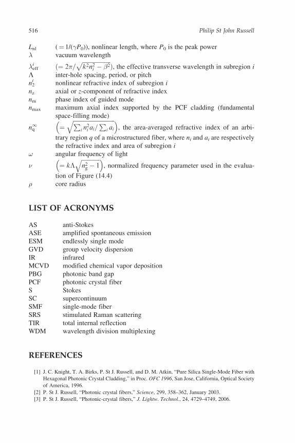
Lnl ( = 1/(�P0)), nonlinear length, where P0 is the peak power
� vacuum wavelength
�effi ð¼ 2�=
ffiffiffiffiffiffiffiffiffiffiffiffiffiffiffiffiffiffiffiffik2n2i � �2
pÞ, the effective transverse wavelength in subregion i
L inter-hole spacing, period, or pitch
n2i nonlinear refractive index of subregion i
nz axial or z-component of refractive index
nm phase index of guided mode
nmax maximum axial index supported by the PCF cladding (fundamental
space-filling mode)
nq1 ¼
ffiffiffiffiffiffiffiffiffiffiffiffiffiffiffiffiffiffiffiffiffiffiffiffiffiffiffiffiffiPi n
2i ai=
Pi ai
q� �, the area-averaged refractive index of an arbi-
trary region q of a microstructured fiber, where ni and ai are respectively
the refractive index and area of subregion i
! angular frequency of light
¼ k�ffiffiffiffiffiffiffiffiffiffiffiffiffin2g � 1
q� �, normalized frequency parameter used in the evalua-
tion of Figure (14.4)
� core radius
LIST OF ACRONYMS
AS anti-Stokes
ASE amplified spontaneous emission
ESM endlessly single mode
GVD group velocity dispersion
IR infrared
MCVD modified chemical vapor deposition
PBG photonic band gap
PCF photonic crystal fiber
S Stokes
SC supercontinuum
SMF single-mode fiber
SRS stimulated Raman scattering
TIR total internal reflection
WDM wavelength division multiplexing
REFERENCES
[1] J. C. Knight, T. A. Birks, P. St J. Russell, and D. M. Atkin, “Pure Silica Single-Mode Fiber with
Hexagonal Photonic Crystal Cladding,” in Proc. OFC 1996, San Jose, California, Optical Society
of America, 1996.
[2] P. St J. Russell, “Photonic crystal fibers,” Science, 299, 358–362, January 2003.
[3] P. St J. Russell, “Photonic-crystal fibers,” J. Lightw. Technol., 24, 4729–4749, 2006.
516 Philip St John Russell
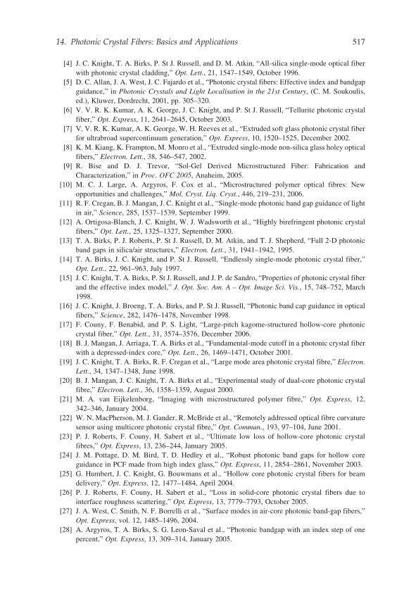
[4] J. C. Knight, T. A. Birks, P. St J. Russell, and D. M. Atkin, “All-silica single-mode optical fiber
with photonic crystal cladding,” Opt. Lett., 21, 1547–1549, October 1996.
[5] D. C. Allan, J. A. West, J. C. Fajardo et al., “Photonic crystal fibers: Effective index and bandgap
guidance,” in Photonic Crystals and Light Localisation in the 21st Century, (C. M. Soukoulis,
ed.), Kluwer, Dordrecht, 2001, pp. 305–320.
[6] V. V. R. K. Kumar, A. K. George, J. C. Knight, and P. St J. Russell, “Tellurite photonic crystal
fiber,” Opt. Express, 11, 2641–2645, October 2003.
[7] V. V. R. K. Kumar, A. K. George, W. H. Reeves et al., “Extruded soft glass photonic crystal fiber
for ultrabroad supercontinuum generation,” Opt. Express, 10, 1520–1525, December 2002.
[8] K. M. Kiang, K. Frampton, M. Monro et al., “Extruded single-mode non-silica glass holey optical
fibers,” Electron. Lett., 38, 546–547, 2002.
[9] R. Bise and D. J. Trevor, “Sol-Gel Derived Microstructured Fiber: Fabrication and
Characterization,” in Proc. OFC 2005, Anaheim, 2005.
[10] M. C. J. Large, A. Argyros, F. Cox et al., “Microstructured polymer optical fibres: New
opportunities and challenges,” Mol. Cryst. Liq. Cryst., 446, 219–231, 2006.
[11] R. F. Cregan, B. J. Mangan, J. C. Knight et al., “Single-mode photonic band gap guidance of light
in air,” Science, 285, 1537–1539, September 1999.
[12] A. Ortigosa-Blanch, J. C. Knight, W. J. Wadsworth et al., “Highly birefringent photonic crystal
fibers,” Opt. Lett., 25, 1325–1327, September 2000.
[13] T. A. Birks, P. J. Roberts, P. St J. Russell, D. M. Atkin, and T. J. Shepherd, “Full 2-D photonic
band gaps in silica/air structures,” Electron. Lett., 31, 1941–1942, 1995.
[14] T. A. Birks, J. C. Knight, and P. St J. Russell, “Endlessly single-mode photonic crystal fiber,”
Opt. Lett., 22, 961–963, July 1997.
[15] J. C. Knight, T. A. Birks, P. St J. Russell, and J. P. de Sandro, “Properties of photonic crystal fiber
and the effective index model,” J. Opt. Soc. Am. A – Opt. Image Sci. Vis., 15, 748–752, March
1998.
[16] J. C. Knight, J. Broeng, T. A. Birks, and P. St J. Russell, “Photonic band cap guidance in optical
fibers,” Science, 282, 1476–1478, November 1998.
[17] F. Couny, F. Benabid, and P. S. Light, “Large-pitch kagome-structured hollow-core photonic
crystal fiber,” Opt. Lett., 31, 3574–3576, December 2006.
[18] B. J. Mangan, J. Arriaga, T. A. Birks et al., “Fundamental-mode cutoff in a photonic crystal fiber
with a depressed-index core,” Opt. Lett., 26, 1469–1471, October 2001.
[19] J. C. Knight, T. A. Birks, R. F. Cregan et al., “Large mode area photonic crystal fibre,” Electron.
Lett., 34, 1347–1348, June 1998.
[20] B. J. Mangan, J. C. Knight, T. A. Birks et al., “Experimental study of dual-core photonic crystal
fibre,” Electron. Lett., 36, 1358–1359, August 2000.
[21] M. A. van Eijkelenborg, “Imaging with microstructured polymer fibre,” Opt. Express, 12,
342–346, January 2004.
[22] W. N. MacPherson, M. J. Gander, R. McBride et al., “Remotely addressed optical fibre curvature
sensor using multicore photonic crystal fibre,” Opt. Commun., 193, 97–104, June 2001.
[23] P. J. Roberts, F. Couny, H. Sabert et al., “Ultimate low loss of hollow-core photonic crystal
fibres,” Opt. Express, 13, 236–244, January 2005.
[24] J. M. Pottage, D. M. Bird, T. D. Hedley et al., “Robust photonic band gaps for hollow core
guidance in PCF made from high index glass,” Opt. Express, 11, 2854–2861, November 2003.
[25] G. Humbert, J. C. Knight, G. Bouwmans et al., “Hollow core photonic crystal fibers for beam
delivery,” Opt. Express, 12, 1477–1484, April 2004.
[26] P. J. Roberts, F. Couny, H. Sabert et al., “Loss in solid-core photonic crystal fibers due to
interface roughness scattering,” Opt. Express, 13, 7779–7793, October 2005.
[27] J. A. West, C. Smith, N. F. Borrelli et al., “Surface modes in air-core photonic band-gap fibers,”
Opt. Express, vol. 12, 1485–1496, 2004.
[28] A. Argyros, T. A. Birks, S. G. Leon-Saval et al., “Photonic bandgap with an index step of one
percent,” Opt. Express, 13, 309–314, January 2005.
14. Photonic Crystal Fibers: Basics and Applications 517
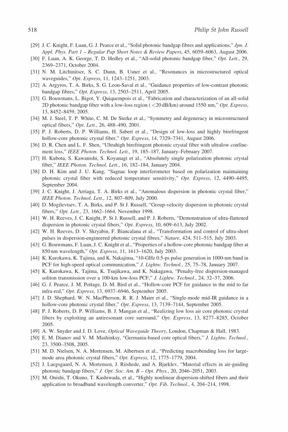
[29] J. C. Knight, F. Luan, G. J. Pearce et al., “Solid photonic bandgap fibres and applications,” Jpn. J.
Appl. Phys. Part 1 – Regular Pap Short Notes & Review Papers, 45, 6059–6063, August 2006.
[30] F. Luan, A. K. George, T. D. Hedley et al., “All-solid photonic bandgap fiber,” Opt. Lett., 29,
2369–2371, October 2004.
[31] N. M. Litchinitser, S. C. Dunn, B. Usner et al., “Resonances in microstructured optical
waveguides,” Opt. Express, 11, 1243–1251, 2003.
[32] A. Argyros, T. A. Birks, S. G. Leon-Saval et al., “Guidance properties of low-contrast photonic
bandgap fibres,” Opt. Express, 13, 2503–2511, April 2005.
[33] G. Bouwmans, L. Bigot, Y. Quiquempois et al., “Fabrication and characterization of an all-solid
2D photonic bandgap fiber with a low-loss region (<20 dB/km) around 1550 nm,” Opt. Express,
13, 8452–8459, 2005.
[34] M. J. Steel, T. P. White, C. M. De Sterke et al., “Symmetry and degeneracy in microstructured
optical fibers,” Opt. Lett., 26, 488–490, 2001.
[35] P. J. Roberts, D. P. Williams, H. Sabert et al., “Design of low-loss and highly birefringent
hollow-core photonic crystal fiber,” Opt. Express, 14, 7329–7341, August 2006.
[36] D. R. Chen and L. F. Shen, “Ultrahigh birefringent photonic crystal fiber with ultralow confine-
ment loss,” IEEE Photon. Technol. Lett., 19, 185–187, January–February 2007.
[37] H. Kubota, S. Kawanishi, S. Koyanagi et al., “Absolutely single polarization photonic crystal
fiber,” IEEE Photon. Technol. Lett., 16, 182–184, January 2004.
[38] D. H. Kim and J. U. Kang, “Sagnac loop interferometer based on polarization maintaining
photonic crystal fiber with reduced temperature sensitivity,” Opt. Express, 12, 4490–4495,
September 2004.
[39] J. C. Knight, J. Arriaga, T. A. Birks et al., “Anomalous dispersion in photonic crystal fiber,”
IEEE Photon. Technol. Lett., 12, 807–809, July 2000.
[40] D. Mogilevtsev, T. A. Birks, and P. St J. Russell, “Group-velocity dispersion in photonic crystal
fibers,” Opt. Lett., 23, 1662–1664, November 1998.
[41] W. H. Reeves, J. C. Knight, P. St J. Russell, and P. J. Roberts, “Demonstration of ultra-flattened
dispersion in photonic crystal fibers,” Opt. Express, 10, 609–613, July 2002.
[42] W. H. Reeves, D. V. Skryabin, F. Biancalana et al., “Transformation and control of ultra-short
pulses in dispersion-engineered photonic crystal fibres,” Nature, 424, 511–515, July 2003.
[43] G. Bouwmans, F. Luan, J. C. Knight et al., “Properties of a hollow-core photonic bandgap fiber at
850 nm wavelength,” Opt. Express, 11, 1613–1620, July 2003.
[44] K. Kurokawa, K. Tajima, and K. Nakajima, “10-GHz 0.5-ps pulse generation in 1000-nm band in
PCF for high-speed optical communication,” J. Lightw. Technol., 25, 75–78, January 2007.
[45] K. Kurokawa, K. Tajima, K. Tsujikawa, and K. Nakagawa, “Penalty-free dispersion-managed
soliton transmission over a 100-km low-loss PCF,” J. Lightw. Technol., 24, 32–37, 2006.
[46] G. J. Pearce, J. M. Pottage, D. M. Bird et al., “Hollow-core PCF for guidance in the mid to far
infra-red,” Opt. Express, 13, 6937–6946, September 2005.
[47] J. D. Shephard, W. N. MacPherson, R. R. J. Maier et al., “Single-mode mid-IR guidance in a
hollow-core photonic crystal fiber,” Opt. Express, 13, 7139–7144, September 2005.
[48] P. J. Roberts, D. P. Williams, B. J. Mangan et al., “Realizing low loss air core photonic crystal
fibers by exploiting an antiresonant core surround,” Opt. Express, 13, 8277–8285, October
2005.
[49] A. W. Snyder and J. D. Love, Optical Waveguide Theory, London, Chapman & Hall, 1983.
[50] E. M. Dianov and V. M. Mashinksy, “Germania-based core optical fibers,” J. Lightw. Technol.,
23, 3500–3508, 2005.
[51] M. D. Nielsen, N. A. Mortensen, M. Albertsen et al., “Predicting macrobending loss for large-
mode area photonic crystal fibers,” Opt. Express, 12, 1775–1779, 2004.
[52] J. Laegsgaard, N. A. Mortensen, J. Riishede, and A. Bjarklev, “Material effects in air-guiding
photonic bandgap fibers,” J. Opt. Soc. Am. B – Opt. Phys., 20, 2046–2051, 2003.
[53] M. Onishi, T. Okuno, T. Kashiwada, et al., “Highly nonlinear dispersion-shifted fibers and their
application to broadband wavelength converter,” Opt. Fib. Technol., 4, 204–214, 1998.
518 Philip St John Russell
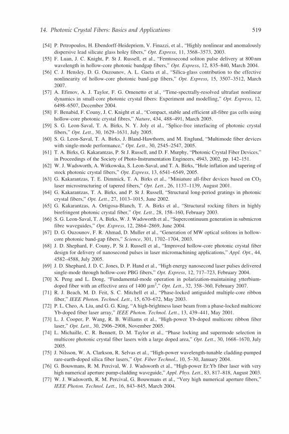
[54] P. Petropoulos, H. Ebendorff-Heidepriem, V. Finazzi, et al., “Highly nonlinear and anomalously
dispersive lead silicate glass holey fibers,” Opt. Express, 11, 3568–3573, 2003.
[55] F. Luan, J. C. Knight, P. St J. Russell, et al., “Femtosecond soliton pulse delivery at 800 nm
wavelength in hollow-core photonic bandgap fibers,” Opt. Express, 12, 835–840, March 2004.
[56] C. J. Hensley, D. G. Ouzounov, A. L. Gaeta et al., “Silica-glass contribution to the effective
nonlinearity of hollow-core photonic band-gap fibers,” Opt. Express, 15, 3507–3512, March
2007.
[57] A. Efimov, A. J. Taylor, F. G. Omenetto et al., “Time-spectrally-resolved ultrafast nonlinear
dynamics in small-core photonic crystal fibers: Experiment and modelling,” Opt. Express, 12,
6498–6507, December 2004.
[58] F. Benabid, F. Couny, J. C. Knight et al., “Compact, stable and efficient all-fibre gas cells using
hollow-core photonic crystal fibres,” Nature, 434, 488–491, March 2005.
[59] S. G. Leon-Saval, T. A. Birks, N. Y. Joly et al., “Splice-free interfacing of photonic crystal
fibers,” Opt. Lett., 30, 1629–1631, July 2005.
[60] S. G. Leon-Saval, T. A. Birks, J. Bland-Hawthorn, and M. Englund, “Multimode fiber devices
with single-mode performance,” Opt. Lett., 30, 2545–2547, 2005.
[61] T. A. Birks, G. Kakarantzas, P. St J. Russell, and D. F. Murphy, “Photonic Crystal Fiber Devices,”
in Proceedings of the Society of Photo-Instrumentation Engineers, 4943, 2002, pp. 142–151.
[62] W. J. Wadsworth, A. Witkowska, S. Leon-Saval, and T. A. Birks, “Hole inflation and tapering of
stock photonic crystal fibers,” Opt. Express, 13, 6541–6549, 2005.
[63] G. Kakarantzas, T. E. Dimmick, T. A. Birks et al., “Miniature all-fiber devices based on CO2
laser microstructuring of tapered fibers,” Opt. Lett., 26, 1137–1139, August 2001.
[64] G. Kakarantzas, T. A. Birks, and P. St J. Russell, “Structural long-period gratings in photonic
crystal fibers,” Opt. Lett., 27, 1013–1015, June 2002.
[65] G. Kakarantzas, A. Ortigosa-Blanch, T. A. Birks et al., “Structural rocking filters in highly
birefringent photonic crystal fiber,” Opt. Lett., 28, 158–160, February 2003.
[66] S. G. Leon-Saval, T. A. Birks, W. J. Wadsworth et al., “Supercontinuum generation in submicron
fibre waveguides,” Opt. Express, 12, 2864–2869, June 2004.
[67] D. G. Ouzounov, F. R. Ahmad, D. Muller et al., “Generation of MW optical solitons in hollow-
core photonic band-gap fibers,” Science, 301, 1702–1704, 2003.
[68] J. D. Shephard, F. Couny, P. St J. Russell et al., “Improved hollow-core photonic crystal fiber
design for delivery of nanosecond pulses in laser micromachining applications,” Appl. Opt., 44,
4582–4588, July 2005.
[69] J. D. Shephard, J. D. C. Jones, D. P. Hand et al., “High energy nanosecond laser pulses delivered
single-mode through hollow-core PBG fibers,” Opt. Express, 12, 717–723, February 2004.
[70] X. Peng and L. Dong, “Fundamental-mode operation in polarization-maintaining ytterbium-
doped fiber with an effective area of 1400 mm2,” Opt. Lett., 32, 358–360, February 2007.
[71] R. J. Beach, M. D. Feit, S. C. Mitchell et al., “Phase-locked antiguided multiple-core ribbon
fiber,” IEEE Photon. Technol. Lett., 15, 670–672, May 2003.
[72] P. L. Cheo, A. Liu, and G. G. King, “A high-brightness laser beam from a phase-locked multicore
Yb-doped fiber laser array,” IEEE Photon. Technol. Lett., 13, 439–441, May 2001.
[73] L. J. Cooper, P. Wang, R. B. Williams et al., “High-power Yb-doped multicore ribbon fiber
laser,” Opt. Lett., 30, 2906–2908, November 2005.
[74] L. Michaille, C. R. Bennett, D. M. Taylor et al., “Phase locking and supermode selection in
multicore photonic crystal fiber lasers with a large doped area,” Opt. Lett., 30, 1668–1670, July
2005.
[75] J. Nilsson, W. A. Clarkson, R. Selvas et al., “High-power wavelength-tunable cladding-pumped
rare-earth-doped silica fiber lasers,” Opt. Fiber Technol., 10, 5–30, January 2004.
[76] G. Bouwmans, R. M. Percival, W. J. Wadsworth et al., “High-power Er:Yb fiber laser with very
high numerical aperture pump-cladding waveguide,” Appl. Phys. Lett., 83, 817–818, August 2003.
[77] W. J. Wadsworth, R. M. Percival, G. Bouwmans et al., “Very high numerical aperture fibers,”
IEEE Photon. Technol. Lett., 16, 843–845, March 2004.
14. Photonic Crystal Fibers: Basics and Applications 519
[78] W. J. Wadsworth, R. M. Percival, G. Bouwmans et al., “High power air-clad photonic crystal
fibre laser,” Opt. Express, 11, 48–53, January 2003.
[79] A. Tunnermann, S. Hofer, S. Liem et al., “Power scaling of high-power fiber lasers and
amplifiers,” Laser Phys., 15, 107–117, 2005.
[80] J. Limpert, T. Schreiber, S. Nolte et al., “High-power air-clad large-mode-area photonic crystal
fiber laser,” Opt. Express, 11, 818–823, April 2003.
[81] F. Di Teodoro and C. D. Brooks, “1.1 MW peak-power, 7 W average-power, high-spectral-
brightness, diffraction-limited pulses from a photonic crystal fiber amplifier,” Opt. Lett., 30,
2694–2696, October 2005.
[82] C. D. Brooks and F. Di Teodoro, “Multimegawatt peak-power, single-transverse-mode operation
of a 100 mu m core diameter, Yb-doped rodlike photonic crystal fiber amplifier,” Appl. Phys.
Lett., 89, September 2006.
[83] C. D. Brooks and F. Di Teodoro, “1-mJ energy, 1-MW peak-power, 10-W average-power,
spectrally narrow, diffraction-limited pulses from a photonic-crystal fiber amplifier,” Opt.
Express, 13, 8999–9002, October 2005.
[84] C. J. S. de Matos, S. V. Popov, A. B. Rulkov et al., “All-fiber format compression of frequency
chirped pulses in air-guiding photonic crystal fibers,” Phys. Rev. Lett., 93, September 2004.
[85] J. Limpert, T. Schreiber, S. Nolte et al., “All fiber chirped-pulse amplification system based on
compression in air-guiding photonic band gap fiber,” Opt. Express, 11, 3332–3337, 2003.
[86] G. P. Agrawal, Nonlinear Fiber Optics, Academic Press, San Diego, London, 2001.
[87] R. R. Alfano, The Supercontinuum Laser Source, New York, Springer-Verlag, 1989.
[88] S. V. Chernikov, Y. Zhu, J. R. Taylor, and V. P. Gapontsev, “Supercontinuum self-Q-switched
ytterbium fiber laser,” Opt. Lett., 22, 298–300, 1997.
[89] J. M. Dudley, G. Genty, and S. Coen, “Supercontinuum generation in photonic crystal fiber,”
Rev. Mod. Phys., 78, 1135–1184, October–December 2006.
[90] W. J. Wadsworth, A. Ortigosa-Blanch, J. C. Knight et al., “Supercontinuum generation in
photonic crystal fibers and optical fiber tapers: a novel light source,” J. Opt. Soc. Am. B – Opt.
Physics, 19, 2148–2155, September 2002.
[91] J. K. Ranka, R. S. Windeler, and A. J. Stentz, “Visible continuum generation in air–silica
microstructure optical fibers with anomalous dispersion at 800 nm,” Opt. Lett., 25, 25–27, 2000.
[92] G. Humbert, W. J. Wadsworth, S. G. Leon-Saval et al., “Supercontinuum generation system for
optical coherence tomography based on tapered photonic crystal fibre,” Opt. Express, 14,
1596–1603, February 2006.
[93] I. Hartl, X. D. Li, C. Chudoba et al., “Ultrahigh-resolution optical coherence tomography using
continuum generation in an air-silica microstructure optical fiber,” Opt. Lett., 26, 608–610,
May 2001.
[94] H. Hundertmark, D. Kracht, D. Wandt, et al., “Supercontinuum generation with 200 pJ laser
pulses in an extruded SF6 fiber at 1560 nm,” Opt. Express, 11, 3196–3201, December 2003.
[95] R. Holzwarth, T. Udem, T. W. Haensch, et al., “Optical frequency synthesizer for precision
spectroscopy,” Phys. Rev. Lett., 85, 2264–2267, September 2000.
[96] S. Coen, A. H. L. Chau, R. Leonhardt, et al., “Supercontinuum generation by stimulated Raman
scattering and parametric four-wave mixing in photonic crystal fibers,” J. Opt. Soc. Am. B – Opt.
Phys., 19, 753–764, April 2002.
[97] W. J. Wadsworth, N. Joly, J. C. Knight et al., “Supercontinuum and four-wave mixing with
Q-switched pulses in endlessly single-mode photonic crystal fibres,” Opt. Express, 12, 299–309,
January 2004.
[98] Fianium Limited, www.fianium.com.
[99] F. G. Omenetto, N. A. Wolchover, M. R. Wehner et al., “Spectrally smooth supercontinuum from
350 nm to 3 um in sub-centimeter lengths of soft-glass photonic crystal fibers,” Opt. Express, 14,
4928–4934, May 2006.
[100] M. Yu, C. J. McKinstrie, and G. P. Agrawal, “Modulational instabilities in dispersion-flattened
fibers,” Phys. Rev. E, 52, 1072–1080, 1995.
520 Philip St John Russell
[101] A. Y. H. Chen, G. K. L. Wong, S. G. Murdoch et al., “Widely tunable optical parametric
generation in a photonic crystal fiber,” Opt. Lett., 30, 762–764, April 2005.
[102] Y. J. Deng, Q. Lin, F. Lu et al., “Broadly tunable femtosecond parametric oscillator using a
photonic crystal fiber,” Opt. Lett., 30, 1234–1236, May 2005.
[103] J. Lasri, P. Devgan, R. Y. Tang et al., “A microstructure-fiber-based 10-GHz synchronized
tunable optical parametric oscillator in the 1550-nm regime,” IEEE Photon. Technol. Lett., 15,
1058–1060, August 2003.
[104] J. E. Sharping, M. Fiorentino, P. Kumar, and R. S. Windeler, “Optical parametric oscillator based
on four-wave mixing in microstructure fiber,” Opt. Lett., 27, 1675–1677, October 2002.
[105] J. D. Harvey, R. Leonhardt, S. Coen et al., “Scalar modulation instability in the normal dispersion
regime by use of a photonic crystal fiber,” Opt. Lett., 28, 2225–2227, November 2003.
[106] J. Fan and A. Migdall, “A broadband high spectral brightness fiber-based two-photon source,”
Opt. Express, 15, 2915–2920, March 2007.
[107] J. G. Rarity, J. Fulconis, J. Duligall et al., “Photonic crystal fiber source of correlated photon
pairs,” Opt. Express, 13, 534–544, January 2005.
[108] J. Fulconis, O. Alibart, W. J. Wadsworth et al., “High brightness single mode source of correlated
photon pairs using a photonic crystal fiber,” Opt. Express, 13, 7572–7582, September 2005.
[109] D. V. Skryabin, F. Luan, J. C. Knight, and P. St J. Russell, “Soliton self-frequency shift
cancellation in photonic crystal fibers,” Science, 301, 1705–1708, September 2003.
[110] N. Y. Joly, F. G. Omenetto, A. Efimov et al., “Competition between spectral splitting and Raman
frequency shift in negative-dispersion slope photonic crystal fiber,” Opt. Commun., 248,
281–285, April 2005.
[111] F. Luan, D. V. Skryabin, A. V. Yulin, and J. C. Knight, “Energy exchange between colliding
solitons in photonic crystal fibers,” Opt. Express, 14, 9844–9853, October 2006.
[112] A. Podlipensky, P. Szarniak, N. Y. Joly et al., “Bound soliton pairs in photonic crystal fiber,”
Opt. Express, 15, 1653–1662, Feburary 2007.
[113] V. Laude, A. Khelif, S. Benchbane et al., “Phononic band-gap guidance of acoustic modes in
photonic crystal fibers,” Phys. Rev. B, 71, 045107, 2005.
[114] S. Guenneau and A. B. Movchan, “Analysis of elastic band structures for oblique incidence,”
Arch. Rational Mech. Anal., 171, 129–150, 2004.
[115] P. St J. Russell, E. Marin, A. Diez et al., “Sonic band gaps in PCF preforms: enhancing the
interaction of sound and light,” Opt. Express, 11, 2555–2560, October 2003.
[116] P. St J. Russell, “Light in a tight space: enhancing matter-light interactions using photonic
crystals,” in Proc. NOC 2002, Hawaii, 2002, pp. 377–379.
[117] P. Dainese, P. St J. Russell, N. Joly et al., “Stimulated Brillouin scattering from multi-GHz-
guided acoustic phonons in nanostructured photonic crystal fibres,” Nat. Phy., 2, 388–392, June
2006.
[118] J. C. Beugnot, T. Sylvestre, H. Maillotte et al., “Guided acoustic wave Brillouin scattering in
photonic crystal fibers,” Opt. Lett., 32, 17–19, January 2007.
[119] P. Dainese, P. St J. Russell, G. S. Wiederhecker et al., “Raman-like light scattering from acoustic
phonons in photonic crystal fiber,” Opt. Express, 14, 4141–4150, May 2006.
[120] P. Rabinowitz, A. Stein, R. Brickman, and A. Kaldor, “Efficient tunable hydrogen Raman laser,”
Appl. Phys. Lett., 35, 739–741, 1979.
[121] L. S. Meng, K. S. Repasky, P. A. Roos, and J. L. Carlsten, “Widely tunable continuous-wave
Raman laser in diatomic hydrogen pumped by an external-cavity diode laser,” Opt. Lett., 25,
472–474, 2000.
[122] F. Benabid, J. C. Knight, G. Antonopoulos, and P. St J. Russell, “Stimulated Raman scattering in
hydrogen-filled hollow-core photonic crystal fiber,” Science, 298, 399–402, October 2002.
[123] F. Benabid, G. Bouwmans, J. C. Knight, et al., “Ultrahigh efficiency laser wavelength conversion
in a gas-filled hollow core photonic crystal fiber by pure stimulated rotational Raman scattering
in molecular hydrogen,” Phys. Rev. Lett., 93, September 2004.
14. Photonic Crystal Fibers: Basics and Applications 521
[124] T. Brabec and F. Krausz, “Intense few-cycle laser fields: Frontiers of nonlinear optics,” Rev.
Mod. Phys., 72, 545–591, 2000.
[125] A. Paul, R. A. Bartels, R. Tobey et al., “Quasi-phase-matched generation of coherent extreme-
ultraviolet light,” Nature, 421, 51–54, 2003.
[126] F. Couny, P. S. Light, F. Benabid, and P. St J. Russell, “Electromagnetically induced transpar-
ency and saturable absorption in all-fiber devices based on 12C2H2-filled hollow-core photonic
crystal fiber,” Opt. Commun., 263, 28–31, July 2006.
[127] S. Ghosh, J. H. Sharp, D. G. Ouzounov, and A. L. Gaeta, “Resonant optical interactions with
molecules confined in photonic band-gap fibers,” Phys. Rev. Lett., 94, 093902, 2005.
[128] K. Nakajima, K. Hogari, J. Zhou et al., “Hole-assisted fiber design for small bending and splice
losses,” IEEE Photon. Technol. Lett., 15, 1737–1739, 2003.
[129] P. J. Roberts, B. Mangan, H. Sabert et al., “Control of dispersion in photonic crystal fibers,”
J. Opt. Fib. Commun. Rep., 2, 435–461, 2005.
[130] R. Kashyap, Fiber Bragg Gratings, Academic Press, San Diego, 1999.
[131] S. J. Mihailov, D. Grobnic, H. M. Ding et al., “Femtosecond IR laser fabrication of Bragg
gratings in photonic crystal fibers and tapers,” IEEE Photon. Technol. Lett., 18, 1837–1839,
September–October 2006.
[132] D. N. Nikogosyan, “Multi-photon high-excitation-energy approach to fibre grating inscription,”
Meas. Sci. Technol., 18, R1–R29, January 2007.
[133] H. Dobb, D. J. Webb, K. Kalli et al., “Continuous wave ultraviolet light-induced fiber Bragg
gratings in few- and single-mode microstructured polymer optical fibers,” Opt. Lett., 30,
3296–3298, December 2005.
[134] A. Ashkin, “Acceleration and trapping of particles by radiation pressure,” Phys. Rev. Lett., 24,
156–159, 1970.
[135] M. J. Renn, R. Pastel, and H. J. Lewandowski, “Laser guidance and trapping of mesoscale
particles in hollow-core optical fibers,” Phys. Rev. Lett., 82, 1574–1577, 1999.
[136] M. J. Renn, D. Montgomery, O. Vdovin et al., “Laser-guided atoms in hollow-core optical fiber,”
Phys. Rev. Lett., 75, 3253–3256, 1995.
[137] F. Benabid, J. C. Knight, and P. St J. Russell, “Particle levitation and guidance in hollow-core
photonic crystal fiber,” Opt. Express, 10, 1195–1203, October 2002.
[138] T. M. Monro, W. Belardi, K. Furusawa et al., “Sensing with microstructured optical fibres,”
Meas. Sci. Technol., 12, 854–858, 2001.
[139] W. N. MacPherson, E. J. Rigg, J. D. C. Jones et al., “Finite-element analysis and experimental
results for a microstructured fiber with enhanced hydrostatic pressure sensitivity,” J. Lightw.
Technol., 23, 1227–1231, March 2005.
[140] P. M. Blanchard, J. G. Burnett, G. R. G. Erry et al., “Two-dimensional bend sensing with a single,
multi-core optical fibre,” Smart Mater. Struct., 9, 132–140, April 2000.
[141] W. N. MacPherson, J. D. C. Jones, B. J. Mangan et al., “Two-core photonic crystal fibre for
Doppler difference velocimetry,” Opt. Commun., 223, 375–380, August 2003.
[142] M. T. Myaing, J. Y. Ye, T. B. Norris et al., “Enhanced two-photon biosensing with double-clad
photonic crystal fibers,” Opt. Lett., 28, 1224–1226, July 2003.
[143] C. E. Finlayson, A. Amezcua-Correa, P. J. A. Sazio et al., “Electrical and Raman characterization
of silicon and germanium-filled microstructured optical fibers,” Appl. Phys. Lett., 90, March
2007.
[144] P. J. A. Sazio, A. Amezcua-Correa, C. E. Finlayson et al., “Microstructured optical fibers as high-
pressure microfluidic reactors,” Science, 311, 1583–1586, 2006.
522 Philip St John Russell
15Specialty fibers for opticalcommunication systems
Ming-Jun Li, Xin Chen, Daniel A. Nolan, Ji Wang,
James A. West, and Karl W. Koch
Corning Inc., Corning, NY, USA
15.1 INTRODUCTION
Optical fiber communications have changed our lives in many ways over the last
40 years. There is no doubt that low-loss optical transmission fibers have been critical
to the enormous success of optical communications technology. It is less well known
however, that fiber-based components have also played a critical role in this success.
Initially, fiber optic transmission systems were point to point systems, with lengths
significantly less than 100 km. Then in the 1980s, rapid progress was made on the
research and understanding of optical components including fiber components. Many of
these fiber components found commercial applications in optical sensor technology
such as in fiber gyroscopes and other optical sensor devices. Simple components such as
power splitters, polarization controllers, multiplexing components, interferometric
devices, and other optical components proved to be very useful. A significant number
of these components were fabricated from polarization maintaining fibers (PMFs).
Although not a large market, optical fiber sensor applications spurred research into
the fabrication of new components such as polarization multiplexers for the optical
gyroscope, for example. Apart from these polarization maintaining components, other
components such as power splitters were fabricated from standard multimode (MM) or
single-mode telecommunication fiber. In the telecommunication sector, the so-called
passive optical network was proposed for the already envisioned fiber-to-the-home
(FTTH) network. This network relied heavily on the use of passive optical splitters.
These splitters were fabricated from standard single-mode fibers (SMFs). Although
FTTH, at a large scale, did not occur until decades later, research into the use of
components for telecommunications applications continued.
Optical Fiber Telecommunications V A: Components and Subsystems
Copyright � 2008, Elsevier Inc. All rights reserved.
ISBN: 978-0-12-374171-4 523
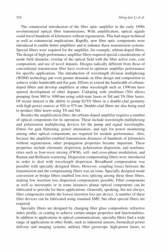
The commercial introduction of the fiber optic amplifier in the early 1990s
revolutionized optical fiber transmissions. With amplification, optical signals
could travel hundreds of kilometers without regeneration. This had major technical
as well as commercial implications. Rapidly, new fiber optic components were
introduced to enable better amplifiers and to enhance these transmission systems.
Special fibers were required for the amplifier, for example, erbium-doped fibers.
The design of high-performance amplifier fibers required special considerations of
mode field diameter, overlap of the optical field with the fiber active core, core
composition, and use of novel dopants. Designs radically different from those of
conventional transmission fiber have evolved to optimize amplifier performance
for specific applications. The introduction of wavelength division multiplexing
(WDM) technology put even greater demands on fiber design and composition to
achieve wider bandwidth and flat gain. Efforts to extend the bandwidth of erbium-
doped fibers and develop amplifiers at other wavelength such as 1300 nm have
spurred development of other dopants. Codoping with ytterbium (Yb) allows
pumping from 900 to 1090 nm using solid-state lasers or Nd and Yb fiber lasers.
Of recent interest is the ability to pump Er/Yb fibers in a double-clad geometry
with high power sources at 920 or 975 nm. Double-clad fibers are also being used
to produce fiber lasers using Yb and Nd.
Besides the amplification fiber, the erbium-doped amplifier requires a number
of optical components for its operation. These include wavelength multiplexing
and polarization multiplexing devices for the pump and signal wavelengths.
Filters for gain flattening, power attenuators, and taps for power monitoring
among other optical components are required for module performance. Also,
because the amplifier-enabled transmission distances of hundreds of kilometers
without regeneration, other propagation properties became important. These
properties include chromatic dispersion, polarization dispersion, and nonlinea-
rities such as four-wave mixing (FWM), self- and cross-phase modulation, and
Raman and Brillouin scattering. Dispersion compensating fibers were introduced
in order to deal with wavelength dispersion. Broadband compensation was
possible with specially designed fibers. However, coupling losses between the
transmission and the compensating fibers was an issue. Specially designed mode
conversion or bridge fibers enabled low-loss splicing among these three fibers,
making low insertion loss dispersion compensators possible. Fiber components
as well as microoptic or in some instances planar optical components can be
fabricated to provide for these applications. Generally speaking, but not always,
fiber components enable the lowest insertion loss per device. A number of these
fiber devices can be fabricated using standard SMF, but often special fibers are
required.
Specialty fibers are designed by changing fiber glass composition, refractive
index profile, or coating to achieve certain unique properties and functionalities.
In addition to applications in optical communications, specialty fibers find a wide
range of applications in other fields, such as industrial sensors, biomedical power
delivery and imaging systems, military fiber gyroscope, high-power lasers, to
524 Ming-Jun Li et al.
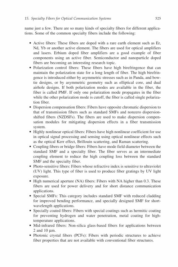
name just a few. There are so many kinds of specialty fibers for different applica-
tions. Some of the common specialty fibers include the following:
• Active fibers: These fibers are doped with a rare earth element such as Er,
Nd, Yb or another active element. The fibers are used for optical amplifiers
and lasers. Erbium doped fiber amplifiers are a good example of fiber
components using an active fiber. Semiconductor and nanoparticle doped
fibers are becoming an interesting research topic.
• Polarization control fibers: These fibers have high birefringence that can
maintain the polarization state for a long length of fiber. The high birefrin-
gence is introduced either by asymmetric stresses such as in Panda, and bow-
tie designs, or by asymmetric geometry such as elliptical core, and dual
airhole designs. If both polarization modes are available in the fiber, the
fiber is called PMF. If only one polarization mode propagates in the fiber
while the other polarization mode is cutoff, the fiber is called single polariza-
tion fiber.
• Dispersion compensation fibers: Fibers have opposite chromatic dispersion to
that of transmission fibers such as standard SMFs and nonzero dispersion-
shifted fibers (NZDSFs). The fibers are used to make dispersion compen-
sation modules for mitigating dispersion effects in a fiber transmission
system.
• Highly nonlinear optical fibers: Fibers have high nonlinear coefficient for use
in optical signal processing and sensing using optical nonlinear effects such
as the optical Kerr effect, Brillouin scattering, and Raman scattering.
• Coupling fibers or bridge fibers: Fibers have mode field diameter between the
standard SMF and a specialty fiber. The fiber serves as an intermediate
coupling element to reduce the high coupling loss between the standard
SMF and the specialty fiber.
• Photo-sensitive fibers: Fibers whose refractive index is sensitive to ultraviolet
(UV) light. This type of fiber is used to produce fiber gratings by UV light
exposure.
• High numerical aperture (NA) fibers: Fibers with NA higher than 0.3. These
fibers are used for power delivery and for short distance communication
applications.
• Special SMFs: This category includes standard SMF with reduced cladding
for improved bending performance, and specially designed SMF for short-
wavelength applications.
• Specially coated fibers: Fibers with special coatings such as hermitic coating
for preventing hydrogen and water penetration, metal coating for high-
temperature applications.
• Mid-infrared fibers: Non-silica glass-based fibers for applications between
2 and 10 mm.
• Photonic crystal fibers (PCFs): Fibers with periodic structures to achieve
fiber properties that are not available with conventional fiber structures.
15. Specialty Fibers for Optical Communication Systems 525
This is by no means an exhaustive list. It is practically impossible to cover all
specialty fiber in one chapter or even in one book. For optical communications-
related specialty fibers, some of them have been discussed in great detail in
previous editions of Optical Fiber Telecommunications. For example, erbium-
doped fibers and amplifiers are discussed in Chapter 2 of the third edition and
Chapter 4 of the fourth edition. Fiber gratings and devices are covered in Chapter 7
of the third edition and Chapter 10 of the fourth edition.
In this chapter, we select a few specialty fiber topics for discussion. Section 2
discusses dispersion compensation fibers. Section 15.3 deals with PMFs and single
polarization fibers (SPFs). Section 15.4 focuses on nonlinear fibers. Section 15.5
describes double-clad fiber for high-power lasers and amplifiers. And the last
section, Section 15.6 covers the topic of photonic crystal fibers.
15.2 DISPERSION COMPENSATION FIBERS
15.2.1 Dispersion Compensation Technologies
High-capacity WDM long-haul transmission systems with large channel counts
(�40 channels) and high channel speeds (�10 Gb/s) are being proposed and
deployed to meet the increasing demand for bandwidth [1–4]. In such systems,
chromatic dispersion is one of the primary limits [5–7]. There are two approaches to
combating the effects of dispersion. One is to design new fibers with reduced
dispersion, and the other is to compensate the dispersion with dispersion compen-
sation modules. Standard SMF with a dispersion of around 17 ps/nm/km at 1550 nm
limits the transmission distance to less than 100 km for a system with 10 Gbit/s bit
rate or higher. To increase the transmission distance, NZDSFs with reduced
dispersion were developed for WDM systems. However, even with NZDSFs,
some dispersion compensation at the terminals is needed for a 10-Gb/s WDM
system with 500-km distance. For a 10-Gbit/s WDM system with a longer reach
or a 40 Gb/s WDM system, both dispersion and dispersion slope compensation are
required.
Different technologies have been proposed to achieve dispersion and dispersion
slope compensation. They can be classified into four categories:
• Dispersion compensation fibers
• Higher order mode dispersion compensation fibers
• Fiber Bragg grating-based devices
• Virtual image-phased array (VIPA)-based devices
• Planar waveguide-based devices
Among the dispersion compensation technologies listed above, dispersion com-
pensation fiber [8–21] is currently the best choice because it has good overall
526 Ming-Jun Li et al.
performance and has been proven to be a reliable solution. Furthermore, large-
scale production processes are available. Although the other technologies possess
some unique features and potentials, they have issues that need to be addressed.
This section discusses dispersion compensation fibers using the fundamental
mode.
15.2.2 Principle of Dispersion Compensating Fibers
Fiber Dispersion
When an optical pulse propagates in an optical fiber, different frequency
components travel with different velocities. The phase velocity is given by
�p =!/�, where ! is the frequency, and � is the propagation constant. The
phase velocity describes the propagation of the phase front. For an optical pulse,
the center of the pulse travels with a speed called group velocity, which is
defined as �g = d!/d�. When a pulse travels though an optical fiber, the time
delay per unit length due to the group velocity is called group delay:
�g = 1/�g = d�/d!. The change of the group delay with frequency results in
fiber dispersion, which is defined as
D =d�gd�
= � 2�c
�
d2�
d!2� �
c
d2neff
d�2(15.1)
where � is the wavelength, c is the speed of light in the vacuum, and the neff is the
effective index of the mode in the fiber. The fiber dispersion causes pulse broad-
ening that limits the transmission data rate.
The fiber dispersion consists of two parts: material dispersion and waveguide
dispersion. For silica-based fiber material doped with Germania (GeO2) or Fluor-
ine, the material dispersion changes slightly with the dopant level and its value is
positive in the wavelength range of interest between 1300 and 1650 nm. The
waveguide dispersion can be changed by fiber profile design and its value can
be either positive or negative.
Fibers that have been installed or are being installed in long-haul systems can
be classified into three categories: standard SMF, dispersion-shifted fiber (DSF),
and NZDSF. The fiber dispersion for these three types of fiber is shown in
Figure 15.1, together with the fiber attenuation curve. These fibers have different
dispersion and dispersion slope values in the 1550-nm window. Table 15.1
compares the values of dispersion, dispersion slope, and dispersion/dispersion
slope ratio of different types of fibers at 1550 nm. It is common to use the �value, that is, the ratio of dispersion to dispersion slope, when describing fiber
dispersion characteristics. The fibers listed in Table 15.1 have � values ranging
from 50 to 300 nm, which means they need different amounts of dispersion and
dispersion slope compensation.
15. Specialty Fibers for Optical Communication Systems 527
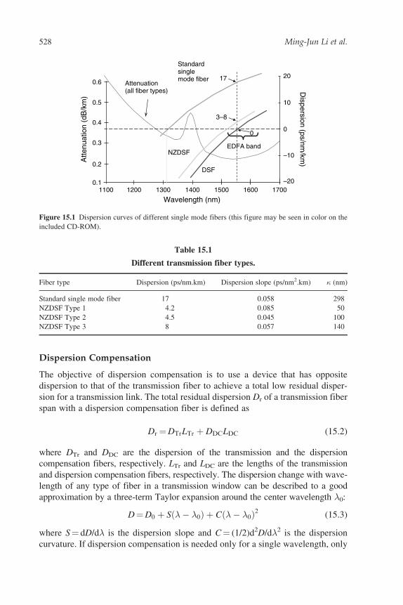
Dispersion Compensation
The objective of dispersion compensation is to use a device that has opposite
dispersion to that of the transmission fiber to achieve a total low residual disper-
sion for a transmission link. The total residual dispersion Dr of a transmission fiber
span with a dispersion compensation fiber is defined as
Dr = DTrLTr þ DDCLDC (15.2)
where DTr and DDC are the dispersion of the transmission and the dispersion
compensation fibers, respectively. LTr and LDC are the lengths of the transmission
and dispersion compensation fibers, respectively. The dispersion change with wave-
length of any type of fiber in a transmission window can be described to a good
approximation by a three-term Taylor expansion around the center wavelength �0:
D = D0 þ Sð�� �0Þ þ Cð�� �0Þ2 (15.3)
where S = dD/d� is the dispersion slope and C = (1/2)d2D/d�2 is the dispersion
curvature. If dispersion compensation is needed only for a single wavelength, only
Dispersion (ps/nm
/km)
0.1
0.2
0.3
0.4
0.5
0.6A
ttenu
atio
n (d
B/k
m)
1100 1200 1300 1400 1500 1600 1700
Wavelength (nm)
DSF
20
EDFA bandNZDSF
Attenuation(all fiber types)
10
0
–10
–20
17
3–8
0
Standardsinglemode fiber
Figure 15.1 Dispersion curves of different single mode fibers (this figure may be seen in color on the
included CD-ROM).
Table 15.1
Different transmission fiber types.
Fiber type Dispersion (ps/nm.km) Dispersion slope (ps/nm2.km) � (nm)
Standard single mode fiber 17 0.058 298
NZDSF Type 1 4.2 0.085 50
NZDSF Type 2 4.5 0.045 100
NZDSF Type 3 8 0.057 140
528 Ming-Jun Li et al.
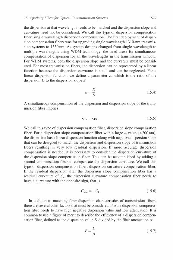
the dispersion at that wavelength needs to be matched and the dispersion slope and
curvature need not be considered. We call this type of dispersion compensation
fiber, single wavelength dispersion compensation. The first deployment of disper-
sion compensation fibers was for upgrading single wavelength 1310-nm transmis-
sion systems to 1550 nm. As system designs changed from single wavelength to
multiple wavelengths using WDM technology, the need arose for simultaneous
compensation of dispersion for all the wavelengths in the transmission window.
For WDM systems, both the dispersion slope and the curvature must be consid-
ered. For most transmission fibers, the dispersion can be represented by a linear
function because the dispersion curvature is small and can be neglected. For a
linear dispersion function, we define a parameter �, which is the ratio of the
dispersion D to the dispersion slope S:
�=D
S(15.4)
A simultaneous compensation of the dispersion and dispersion slope of the trans-
mission fiber implies
�Tr =�DC (15.5)
We call this type of dispersion compensation fiber, dispersion slope compensation
fiber. For a dispersion slope compensation fiber with a large � value (>200 nm),
the dispersion has a linear dispersion function along with negative dispersion slope
that can be designed to match the dispersion and dispersion slope of transmission
fibers resulting in very low residual dispersion. If more accurate dispersion
compensation is needed, it is necessary to consider the dispersion curvature of
the dispersion slope compensation fiber. This can be accomplished by adding a
second compensation fiber to compensate the dispersion curvature. We call this
type of dispersion compensation fiber, dispersion curvature compensation fiber.
If the residual dispersion after the dispersion slope compensation fiber has a
residual curvature of Cr, the dispersion curvature compensation fiber needs to
have a curvature with the opposite sign, that is
CCC =�Cr (15.6)
In addition to matching fiber dispersion characteristics of transmission fibers,
there are several other factors that must be considered. First, a dispersion compensa-
tion fiber needs to have high negative dispersion value and low attenuation. It is
common to use a figure of merit to describe the efficiency of a dispersion compen-
sation fiber, defined as the dispersion value D divided by the fiber attenuation �:
F =D
�(15.7)
15. Specialty Fibers for Optical Communication Systems 529
The figure of merit is related to the attenuation increase in a link due to the
dispersion compensation fiber. The higher the figure of merit is, the lower the
incremental attenuation that is added to the system. The fiber attenuation is affected
by many factors. For an optical fiber, the total attenuation can be expressed by
�=�absorption þ �scattering þ �imperfection þ �bending (15.8)
In Eqn 15.8, �absorption is the attenuation caused by material absorptions at UV
and infrared wavelengths and color centers. �scattering is the attenuation due to linear
scattering that is due to fluctuations in material density and composition. This type
of scattering is also called “Rayleigh scattering.” In addition to linear scattering,
nonlinear scattering can occur, if the power is sufficiently high, which increases
fiber attenuation. The nonlinear scattering includes stimulated Brillouin scattering
(SBS) due to acoustic phonons and stimulated Raman scattering (SRS) due to
optical phonons. The third term is the attenuation due to waveguide imperfections
such as defects and stresses. The last term, �bending is the attenuation due to fiber
bending including both the macro- and the microbending. The absorption loss does
not change much with fiber design for Ge-doped silica fibers. On the other hand,
different profile designs can change the other three terms significantly.
Second, a dispersion compensation fiber needs to have a sufficiently large
effective area to minimize the nonlinear effects introduced to the system. If the
effective area is too small, the nonlinear effects in the dispersion compensation
fiber can introduce system penalty and increase splice losses. In the nonlinear
regime, a higher figure of merit as defined in Eqn 15.7 does not mean that the
system will have better performance. From a nonlinear perspective, a different
figure of merit, the so-called nonlinear figure of merit, is necessary to take into
account the impact of nonlinear effects [22]. The nonlinear figure of merit takes
into consideration the dispersion D, fiber attenuation �, effective area A, and
nonlinear coefficient of both the dispersion compensation fiber and the transmis-
sion fiber, and is defined as follows
Fnl ¼TrDC
ADC
ATr
�DC
�Tr
ðlTr � 1Þ2
lTr
lDC
ðlDC � 1Þ2(15.9)
where lTr = e�TrLTr, lDC = e�DCLDC = e�DCLTrDTr/DDC. The nonlinear figure of merit is
closely related to the system performance. A higher nonlinear figure of merit
results in a lower nonlinear signal degradation. The design of dispersion compen-
sation fiber should aim for increasing the dispersion and effective area while
reducing the attenuation. Because the dispersion and the dispersion slope of
dispersion compensation fiber are controlled by waveguide dispersion, the effec-
tive area tends to become smaller when the dispersion and the dispersion slope
become more negative. It is a challenging task to design a dispersion compensation
fiber with a high figure of merit and a large effective area.
530 Ming-Jun Li et al.
Third, a dispersion compensation fiber must introduce low multiple path inter-
ference (MPI) to the system when splicing to transmissions fibers. MPI happens
when more than one mode propagates in the fiber [23], and the power coupling
between the fundamental mode and the higher-order modes causes the transmitted
power to fluctuate with wavelength. For single-mode dispersion compensation
fibers, this implies the effective cutoff wavelength must be below the operating
window.
Fourth, the polarization mode dispersion (PMD) of a dispersion compensation fiber
must be low. Because of the high delta and small core designs for dispersion
compensation fibers, their PMD values are normally much higher than that of
transmission fibers. Low PMD requires more careful control of the fiber geometry
and stresses during the fiber-manufacturing process. In addition, fiber-spinning tech-
niques can be used to mitigate the PMD of dispersion compensation fibers [24, 25].
15.2.3 Dispersion Compensation Fibers
Fiber Profile Designs
In designing dispersion compensation fibers, one needs to manipulate the fiber
refractive index profile to achieve negative waveguide dispersion and dispersion
slope. The profile designs for dispersion compensation fibers can be grouped into
four design types, as shown in Figure 15.2 [8–21]. Design (a) is a simple step core
with a single cladding that was used in the early days of dispersion compensation
fiber development. The design has two parameters only: the relative core refractive
index change D and the core radius r. Total negative dispersion is achieved by
creating more negative waveguide dispersion to move the zero-dispersion wave-
length to a wavelength longer than the operating wavelength such as 1550 nm.
This is done by adjusting the core delta and core radius. Negative waveguide
dispersion results from the rapid change of power from the core to the cladding
with wavelength. As the wavelength increases, the mode power extends further
(a) (b)
(c) (d)
Figure 15.2 Profile types for dispersion compensation fibers.
15. Specialty Fibers for Optical Communication Systems 531
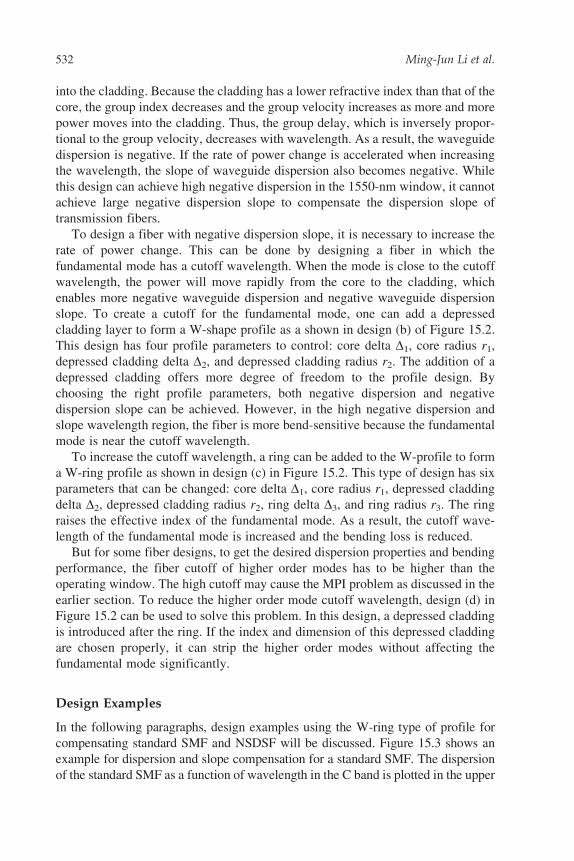
into the cladding. Because the cladding has a lower refractive index than that of the
core, the group index decreases and the group velocity increases as more and more
power moves into the cladding. Thus, the group delay, which is inversely propor-
tional to the group velocity, decreases with wavelength. As a result, the waveguide
dispersion is negative. If the rate of power change is accelerated when increasing
the wavelength, the slope of waveguide dispersion also becomes negative. While
this design can achieve high negative dispersion in the 1550-nm window, it cannot
achieve large negative dispersion slope to compensate the dispersion slope of
transmission fibers.
To design a fiber with negative dispersion slope, it is necessary to increase the
rate of power change. This can be done by designing a fiber in which the
fundamental mode has a cutoff wavelength. When the mode is close to the cutoff
wavelength, the power will move rapidly from the core to the cladding, which
enables more negative waveguide dispersion and negative waveguide dispersion
slope. To create a cutoff for the fundamental mode, one can add a depressed
cladding layer to form a W-shape profile as a shown in design (b) of Figure 15.2.
This design has four profile parameters to control: core delta D1, core radius r1,
depressed cladding delta D2, and depressed cladding radius r2. The addition of a
depressed cladding offers more degree of freedom to the profile design. By
choosing the right profile parameters, both negative dispersion and negative
dispersion slope can be achieved. However, in the high negative dispersion and
slope wavelength region, the fiber is more bend-sensitive because the fundamental
mode is near the cutoff wavelength.
To increase the cutoff wavelength, a ring can be added to the W-profile to form
a W-ring profile as shown in design (c) in Figure 15.2. This type of design has six
parameters that can be changed: core delta D1, core radius r1, depressed cladding
delta D2, depressed cladding radius r2, ring delta D3, and ring radius r3. The ring
raises the effective index of the fundamental mode. As a result, the cutoff wave-
length of the fundamental mode is increased and the bending loss is reduced.
But for some fiber designs, to get the desired dispersion properties and bending
performance, the fiber cutoff of higher order modes has to be higher than the
operating window. The high cutoff may cause the MPI problem as discussed in the
earlier section. To reduce the higher order mode cutoff wavelength, design (d) in
Figure 15.2 can be used to solve this problem. In this design, a depressed cladding
is introduced after the ring. If the index and dimension of this depressed cladding
are chosen properly, it can strip the higher order modes without affecting the
fundamental mode significantly.
Design Examples
In the following paragraphs, design examples using the W-ring type of profile for
compensating standard SMF and NSDSF will be discussed. Figure 15.3 shows an
example for dispersion and slope compensation for a standard SMF. The dispersion
of the standard SMF as a function of wavelength in the C band is plotted in the upper
532 Ming-Jun Li et al.
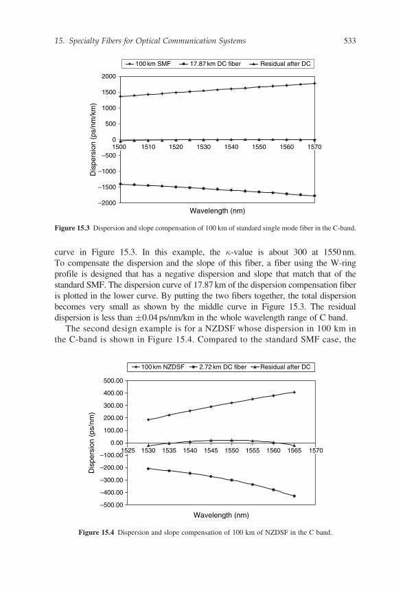
curve in Figure 15.3. In this example, the �-value is about 300 at 1550 nm.
To compensate the dispersion and the slope of this fiber, a fiber using the W-ring
profile is designed that has a negative dispersion and slope that match that of the
standard SMF. The dispersion curve of 17.87 km of the dispersion compensation fiber
is plotted in the lower curve. By putting the two fibers together, the total dispersion
becomes very small as shown by the middle curve in Figure 15.3. The residual
dispersion is less than �0.04 ps/nm/km in the whole wavelength range of C band.
The second design example is for a NZDSF whose dispersion in 100 km in
the C-band is shown in Figure 15.4. Compared to the standard SMF case, the
–2000
–1500
–1000
–500
0
500
1000
1500
2000
1510 1520 1530 1540 1550 1560
Wavelength (nm)
Dis
pers
ion
(ps/
nm/k
m)
100 km SMF 17.87 km DC fiber Residual after DC
15701500
Figure 15.3 Dispersion and slope compensation of 100 km of standard single mode fiber in the C-band.
–500.00
–400.00
–300.00
–200.00
–100.00
0.001525 1530 1535 1540 1545 1550 1555 1560 1565
100.00
200.00
300.00
400.00
500.00
Wavelength (nm)
Dis
pers
ion
(ps/
nm)
100 km NZDSF 2.72 km DC fiber Residual after DC
1570
Figure 15.4 Dispersion and slope compensation of 100 km of NZDSF in the C band.
15. Specialty Fibers for Optical Communication Systems 533
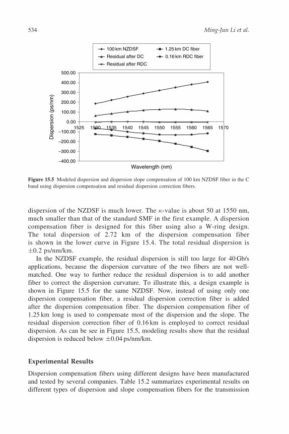
dispersion of the NZDSF is much lower. The �-value is about 50 at 1550 nm,
much smaller than that of the standard SMF in the first example. A dispersion
compensation fiber is designed for this fiber using also a W-ring design.
The total dispersion of 2.72 km of the dispersion compensation fiber
is shown in the lower curve in Figure 15.4. The total residual dispersion is
�0.2 ps/nm/km.
In the NZDSF example, the residual dispersion is still too large for 40 Gb/s
applications, because the dispersion curvature of the two fibers are not well-
matched. One way to further reduce the residual dispersion is to add another
fiber to correct the dispersion curvature. To illustrate this, a design example is
shown in Figure 15.5 for the same NZDSF. Now, instead of using only one
dispersion compensation fiber, a residual dispersion correction fiber is added
after the dispersion compensation fiber. The dispersion compensation fiber of
1.25 km long is used to compensate most of the dispersion and the slope. The
residual dispersion correction fiber of 0.16 km is employed to correct residual
dispersion. As can be see in Figure 15.5, modeling results show that the residual
dispersion is reduced below �0.04 ps/nm/km.
Experimental Results
Dispersion compensation fibers using different designs have been manufactured
and tested by several companies. Table 15.2 summarizes experimental results on
different types of dispersion and slope compensation fibers for the transmission
–400.00
–300.00
–200.00
–100.00
0.00
100.00
200.00
300.00
400.00
500.00
Wavelength (nm)
Dis
pers
ion
(ps/
nm)
100 km NZDSF 1.25 km DC fiber
Residual after DC 0.16 km RDC fiber
Residual after RDC
1530 1535 1540 1545 1550 1555 1560 1565 15701525
Figure 15.5 Modeled dispersion and dispersion slope compensation of 100 km NZDSF fiber in the C
band using dispersion compensation and residual dispersion correction fibers.
534 Ming-Jun Li et al.
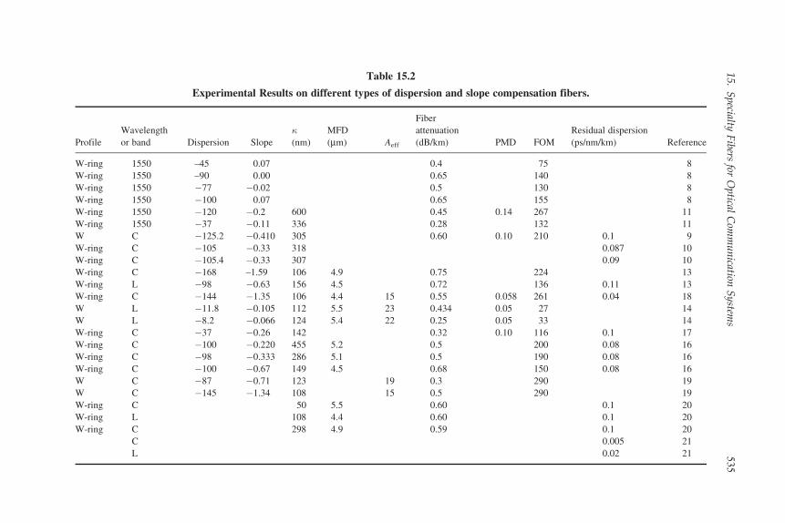
Table 15.2
Experimental Results on different types of dispersion and slope compensation fibers.
Profile
Wavelength
or band Dispersion Slope
�
(nm)
MFD
(mm) Aeff
Fiber
attenuation
(dB/km) PMD FOM
Residual dispersion
(ps/nm/km) Reference
W-ring 1550 –45 0.07 0.4 75 8
W-ring 1550 –90 0.00 0.65 140 8
W-ring 1550 �77 �0.02 0.5 130 8
W-ring 1550 �100 0.07 0.65 155 8
W-ring 1550 �120 �0.2 600 0.45 0.14 267 11
W-ring 1550 �37 �0.11 336 0.28 132 11
W C �125.2 �0.410 305 0.60 0.10 210 0.1 9
W-ring C �105 �0.33 318 0.087 10
W-ring C �105.4 �0.33 307 0.09 10
W-ring C �168 –1.59 106 4.9 0.75 224 13
W-ring L �98 �0.63 156 4.5 0.72 136 0.11 13
W-ring C �144 �1.35 106 4.4 15 0.55 0.058 261 0.04 18
W L �11.8 �0.105 112 5.5 23 0.434 0.05 27 14
W L �8.2 �0.066 124 5.4 22 0.25 0.05 33 14
W-ring C �37 �0.26 142 0.32 0.10 116 0.1 17
W-ring C �100 �0.220 455 5.2 0.5 200 0.08 16
W-ring C �98 �0.333 286 5.1 0.5 190 0.08 16
W-ring C �100 �0.67 149 4.5 0.68 150 0.08 16
W C �87 �0.71 123 19 0.3 290 19
W C �145 �1.34 108 15 0.5 290 19
W-ring C 50 5.5 0.60 0.1 20
W-ring L 108 4.4 0.60 0.1 20
W-ring C 298 4.9 0.59 0.1 20
C 0.005 21
L 0.02 21
15
.S
pecialty
Fibers
forO
ptical
Com
mu
nication
Sy
stems
53
5
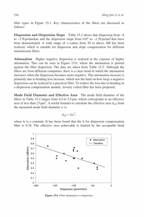
fiber types in Figure 15.1. Key characteristics of the fibers are discussed as
follows:
Dispersion and Dispersion Slope Table 15.2 shows that dispersion from –8
to –178 ps/nm/km and the dispersion slope from 0.07 to –1.59 ps/nm2/km have
been demonstrated. A wide range of �-values from 50 to above 300 has been
realized, which is suitable for dispersion and slope compensation for different
transmission fibers.
Attenuation Higher negative dispersion is realized at the expense of higher
attenuation. This can be seen in Figure 15.6, where the attenuation is plotted
against the fiber dispersion. The data are taken from Table 15.2. Although the
fibers are from different companies, there is a clear trend in which the attenuation
increases when the dispersion becomes more negative. This attenuation increase is
primarily due to bending loss increase, which sets the limit on how large a negative
dispersion can be realized in a practical fiber. To reduce the loss due to bending in
a dispersion compensation module, loosely coiled fiber has been proposed.
Mode Field Diameter and Effective Area The mode field diameter of the
fibers in Table 15.2 ranges from 4.4 to 5.5 mm, which corresponds to an effective
area of less than 23 mm2. A useful formula to calculate the effective area Aeff from
the measured mode field diameter w is
Aeff = kw2;
where k is a constant. It has been found that the k for dispersion compensation
fiber is 0.76. The effective area achievable is limited by the acceptable bend
0–200 –150 –100 –50 0
0.1
0.2
0.3
0.4
0.5
0.6
0.7
0.8
0.9
1
Dispersion (ps/nm/km)
Atte
nuat
ion
(dB
/km
)
Attenuation
Trendline
Figure 15.6 Fiber attenuation vs dispersion.
536 Ming-Jun Li et al.
sensitivity. Because the high dispersion acts to rapidly increase the effective area
as a function of wavelength, the trade-off between effective area and bend loss we
observe in any fiber design is intensified. In order to achieve a fiber with good
bend characteristics, the effective area must be reduced. The result is dispersion
compensation fibers with effective areas less than 20 mm2, although advanced
coating formulations can be leveraged to increase this figure.
Nonlinear Properties Because the nonlinear refractive index n2 of dispersion
compensation fiber is only slightly higher than conventional fiber, the major
factor affecting the nonlinear properties is the effective area. The common
perception is that small effective areas of dispersion compensation fiber are
unacceptable because propagation nonlinearities will be increased. Self-phase
modulation (SPM) and cross-phase modulation (XPM) generated in the disper-
sion compensation fiber are the nonlinear impairments most likely to affect
transmission. SPM is a significant impairment when the power launched per
channel exceeds several milliwatts in a typical dispersion compensation module.
XPM and FWM penalties are observed to be very small compared with transmis-
sion fiber. This is because (1) the fiber has high dispersion and (2) the power
launched into the dispersion compensation fiber is not proportionally higher.
SPM, on the other hand, is a single-channel impairment, which depends more on
the fiber nonlinearity (n2/Aeff) rather than on local dispersion. The nonlinear
response of a typical dispersion compensation module (consisting of several
kilometers of small effective area fiber) is often negligible in long-haul systems
as long as the dispersion compensation module is deployed where the power per
channel is not extremely large. We should note that with the proliferation of
Raman amplification, smaller effective areas in dispersion compensation fibers
may actually prove beneficial.
PMD As discussed earlier, it is a challenge to make dispersion compensation
fibers with low PMD because dispersion compensation fibers are more sensitive to
core deformation than conventional fibers due to the high core delta. To reduce the
PMD in dispersion compensation fibers, extreme care must be taken to reduce core
asymmetry due to geometry and stresses. In addition, a common technique to
improve PMD is to use fiber spinning during the fiber draw. It has been reported
that fiber spinning reduces the effective fiber PMD distribution. The average PMD
is lowered from 0.21 to 0.091 ps/km½, and the standard deviation is reduced from
0.19 to 0.065 ps/km½.
PMD is sensitive to fiber deployment. For dispersion compensation fiber that is
coiled in a dispersion compensation module, the coil diameter has a significant
impact on fiber PMD. In a coiled fiber, fiber bending introduces stress birefrin-
gence. This stress-induced birefringence causes a significant increase in fiber PMD
because dispersion compensation fibers are very sensitive to fiber bending. One
way to reduce the stress-induced birefringence is to reduce the fiber diameter from
the standard 125 mm, for example, to 80 mm. However, a fiber with reduced fiber
15. Specialty Fibers for Optical Communication Systems 537
diameter is more susceptible to microbending loss. In addition, reducing the
cladding diameter does nothing to improve bent fiber form birefringence, another
potentially significant source of birefringence. Both PMD and microbending loss
must be considered in dispersion compensation fiber design. With proper designs
and advanced manufacturing technologies, PMD below 0.1 ps/km½ has been
demonstrated, as summarized in Table 15.2.
Splicing Loss Dispersion compensation fibers have a mode field diameter of
about 5 mm, which is much smaller than the 10.5 mm mode field diameter of
standard SMF. Theoretical calculations show that the coupling loss due to the
mode field mismatch is as high as 2.2 dB. However, practical fusion splice loss
between dispersion compensation fiber and standard SMF is much lower than this
value. This is because doping materials in the core regions will diffuse when the
fiber is heated during the fusion-splicing process, which creates a tapered region
with increased mode field diameter. By optimizing the fusion splice parameters,
the splice loss between dispersion compensation fiber and standard SMF is
reduced to less than 0.25 dB.
15.2.4 Summary
Dispersion compensation fibers were discussed in this section. Design concepts
and physics for achieving negative dispersion and dispersion slope are explained.
Compensation fiber designs for standard SMF and NZDSF fibers are described in
detail.
Results on single mode dispersion compensation fibers from different compa-
nies were reviewed. They show that dispersion compensation fibers with different
dispersion and slope values are possible and can be used for different types of
transmission fibers. With the continuous development of high-data-rate, long-
distance WDM optical networks, it is expected that dispersion will remain an
important issue. As in the past, transmission fiber technologies and dispersion
compensation technologies will work together to mitigate dispersion effects.
Future developments are anticipated in the following areas:
• Dispersion-managed fiber cable systems. In these systems, the cable is made
of matched positive and negative dispersion fibers. By managing the lengths
of the two fibers, optimum system performance can be achieved. Because the
positive and negative dispersion fibers compensate each other, this kind of
system can have very low residual dispersion that can be easily compensated,
if further compensation is needed.
• Continuous improvements in performance of dispersion compensation fibers.
These improvements include increasing the fiber’s effective area, reducing
residual dispersion, and reducing bending and splice losses.
538 Ming-Jun Li et al.
• Dispersion compensation fiber amplifiers. This type of dispersion compen-
sation fiber devices incorporate SRS to compensate both dispersion and
power loss.
• Development of dynamic tunable dispersion compensation devices. For sys-
tems with a bit rate greater than 40 Gb/s, very accurate dispersion control is
required. Such systems will necessitate dynamic tunable dispersion devices
on a channel by channel basis.
• Better understanding of electronic dispersion compensation (EDC) technique
in terms of its capability and limitations. This will enable designing new
transmission and dispersion compensation fibers to work with EDC.
15.3 POLARIZATION MAINTAINING AND SINGLEPOLARIZATION FIBERS
15.3.1 Polarization Effects in Optical Fibers
Although SMFs are often misunderstood to be fibers that can only transmit a
“single” mode by simply taking the words literally, SMFs can actually support two
polarization modes. By one definition [26], SMFs are optical fibers which support
only a single mode per polarization direction at a given wavelength. Each polar-
ization mode has its own effective propagation constant, which can take different
values resulting in polarization effects. Extensive study of polarization effects in
SMF began several decades ago [27]. In the past decade, they received increasing
attention as they can induce significant impairment in higher bit-rate optical
communication systems.
In practice, it is very difficult to make fibers with perfect circular symmetry so
that the two orthogonally polarized HE11 modes have the same propagation
constant. The origin of polarization effects in SMFs is related to the asymmetry
in either the fiber geometry or the stress distribution in the fibers. The latter
results from imperfections in the preform-making process, which could be
modified chemical vapor deposition (MCVD), outside vapor deposition
(OVD), or other processes. The distortion of the geometry of the fiber core
leads directly to different propagation constants or phase velocities in the two
polarization modes. At different radial positions in the fiber, the fiber is formed
with different chemical composition with distinct thermal expansion coeffi-
cients. The distortion in geometry can cause the stress field in the core to become
asymmetric as the fiber is drawn and cooled down from a high temperature.
Through the stress–optic effect, the asymmetric stress is translated into an
anisotropic refractive index change across the fiber. Even after the fiber is
made, the polarization properties of SMFs can be altered through external factors
such as bending, twisting, or applying lateral load to the fibers when the fibers
are deployed for actual use.
15. Specialty Fibers for Optical Communication Systems 539
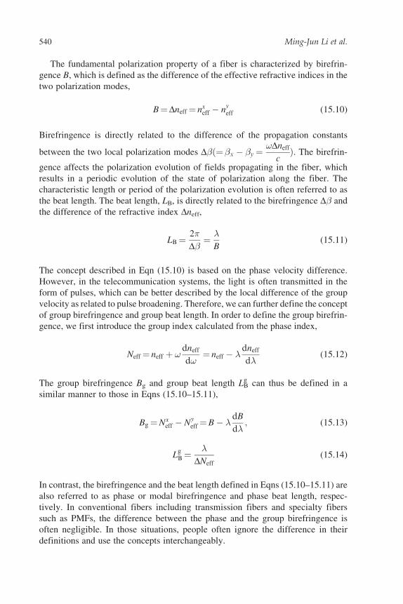
The fundamental polarization property of a fiber is characterized by birefrin-
gence B, which is defined as the difference of the effective refractive indices in the
two polarization modes,
B = Dneff = nxeff � n
yeff (15.10)
Birefringence is directly related to the difference of the propagation constants
between the two local polarization modes D�ð= �x � �y =!Dneff
cÞ. The birefrin-
gence affects the polarization evolution of fields propagating in the fiber, which
results in a periodic evolution of the state of polarization along the fiber. The
characteristic length or period of the polarization evolution is often referred to as
the beat length. The beat length, LB, is directly related to the birefringence D� and
the difference of the refractive index Dneff,
LB =2�
D�=�
B(15.11)
The concept described in Eqn (15.10) is based on the phase velocity difference.
However, in the telecommunication systems, the light is often transmitted in the
form of pulses, which can be better described by the local difference of the group
velocity as related to pulse broadening. Therefore, we can further define the concept
of group birefringence and group beat length. In order to define the group birefrin-
gence, we first introduce the group index calculated from the phase index,
Neff = neff þ !dneff
d!= neff � �
dneff
d�(15.12)
The group birefringence Bg and group beat length LBg can thus be defined in a
similar manner to those in Eqns (15.10–15.11),
Bg = Nxeff � N
yeff = B� � dB
d�; (15.13)
LgB =
�
DNeff(15.14)
In contrast, the birefringence and the beat length defined in Eqns (15.10–15.11) are
also referred to as phase or modal birefringence and phase beat length, respec-
tively. In conventional fibers including transmission fibers and specialty fibers
such as PMFs, the difference between the phase and the group birefringence is
often negligible. In those situations, people often ignore the difference in their
definitions and use the concepts interchangeably.
540 Ming-Jun Li et al.
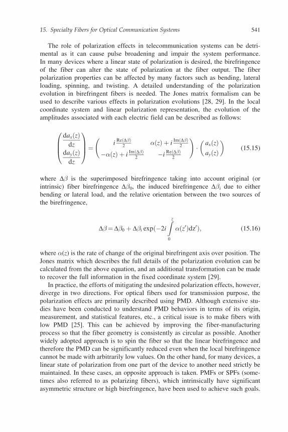
The role of polarization effects in telecommunication systems can be detri-
mental as it can cause pulse broadening and impair the system performance.
In many devices where a linear state of polarization is desired, the birefringence
of the fiber can alter the state of polarization at the fiber output. The fiber
polarization properties can be affected by many factors such as bending, lateral
loading, spinning, and twisting. A detailed understanding of the polarization
evolution in birefringent fibers is needed. The Jones matrix formalism can be
used to describe various effects in polarization evolutions [28, 29]. In the local
coordinate system and linear polarization representation, the evolution of the
amplitudes associated with each electric field can be described as follows:
daxðzÞdz
dayðzÞdz
0BB@
1CCA=
iReðD�Þ
2�ðzÞ þ i
ImðD�Þ2
��ðzÞ þ iImðD�Þ
2�i
ReðD�Þ2
!�
axðzÞayðzÞ
� �(15.15)
where D� is the superimposed birefringence taking into account original (or
intrinsic) fiber birefringence D�0, the induced birefringence D�i due to either
bending or lateral load, and the relative orientation between the two sources of
the birefringence,
D�= D�0 þ D�i expð�2i
Zz
0
�ðz0Þdz0Þ; (15.16)
where �(z) is the rate of change of the original birefringent axis over position. The
Jones matrix which describes the full details of the polarization evolution can be
calculated from the above equation, and an additional transformation can be made
to recover the full information in the fixed coordinate system [29].
In practice, the efforts of mitigating the undesired polarization effects, however,
diverge in two directions. For optical fibers used for transmission purpose, the
polarization effects are primarily described using PMD. Although extensive stu-
dies have been conducted to understand PMD behaviors in terms of its origin,
measurement, and statistical features, etc., a critical issue is to make fibers with
low PMD [25]. This can be achieved by improving the fiber-manufacturing
process so that the fiber geometry is consistently as circular as possible. Another
widely adopted approach is to spin the fiber so that the linear birefringence and
therefore the PMD can be significantly reduced even when the local birefringence
cannot be made with arbitrarily low values. On the other hand, for many devices, a
linear state of polarization from one part of the device to another need strictly be
maintained. In these cases, an opposite approach is taken. PMFs or SPFs (some-
times also referred to as polarizing fibers), which intrinsically have significant
asymmetric structure or high birefringence, have been used to achieve such goals.
15. Specialty Fibers for Optical Communication Systems 541
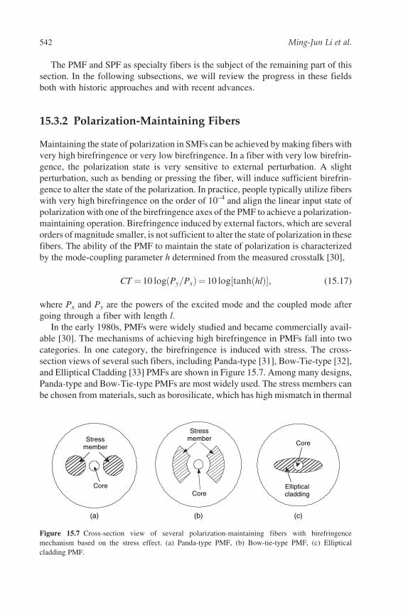
The PMF and SPF as specialty fibers is the subject of the remaining part of this
section. In the following subsections, we will review the progress in these fields
both with historic approaches and with recent advances.
15.3.2 Polarization-Maintaining Fibers
Maintaining the state of polarization in SMFs can be achieved by making fibers with
very high birefringence or very low birefringence. In a fiber with very low birefrin-
gence, the polarization state is very sensitive to external perturbation. A slight
perturbation, such as bending or pressing the fiber, will induce sufficient birefrin-
gence to alter the state of the polarization. In practice, people typically utilize fibers
with very high birefringence on the order of 10–4 and align the linear input state of
polarization with one of the birefringence axes of the PMF to achieve a polarization-
maintaining operation. Birefringence induced by external factors, which are several
orders of magnitude smaller, is not sufficient to alter the state of polarization in these
fibers. The ability of the PMF to maintain the state of polarization is characterized
by the mode-coupling parameter h determined from the measured crosstalk [30],
CT = 10 logðPy=PxÞ= 10 log½tanhðhlÞ�, (15.17)
where Px and Py are the powers of the excited mode and the coupled mode after
going through a fiber with length l.
In the early 1980s, PMFs were widely studied and became commercially avail-
able [30]. The mechanisms of achieving high birefringence in PMFs fall into two
categories. In one category, the birefringence is induced with stress. The cross-
section views of several such fibers, including Panda-type [31], Bow-Tie-type [32],
and Elliptical Cladding [33] PMFs are shown in Figure 15.7. Among many designs,
Panda-type and Bow-Tie-type PMFs are most widely used. The stress members can
be chosen from materials, such as borosilicate, which has high mismatch in thermal
(a)
Stressmember
Core
(b)
Stressmember
Core
(c)
Core
Ellipticalcladding
Figure 15.7 Cross-section view of several polarization-maintaining fibers with birefringence
mechanism based on the stress effect. (a) Panda-type PMF, (b) Bow-tie-type PMF, (c) Elliptical
cladding PMF.
542 Ming-Jun Li et al.
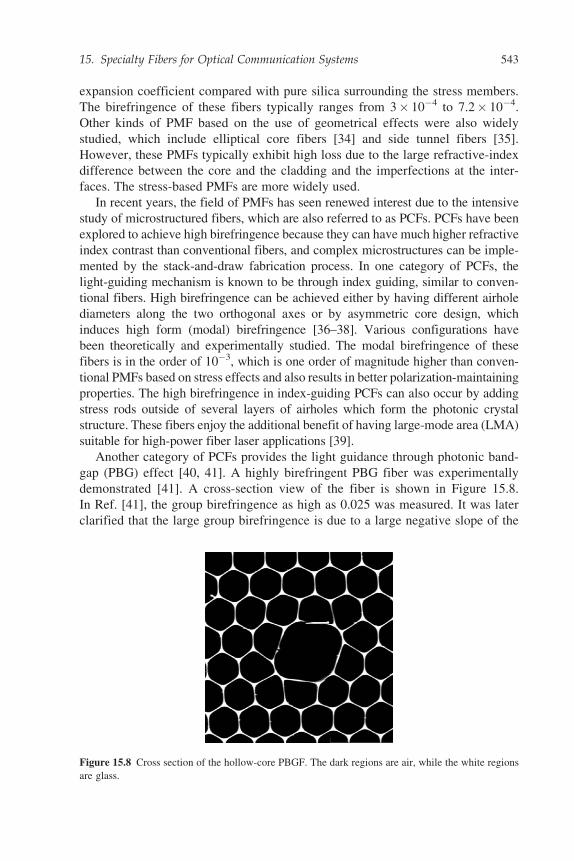
expansion coefficient compared with pure silica surrounding the stress members.
The birefringence of these fibers typically ranges from 3� 10�4 to 7.2� 10�4.
Other kinds of PMF based on the use of geometrical effects were also widely
studied, which include elliptical core fibers [34] and side tunnel fibers [35].
However, these PMFs typically exhibit high loss due to the large refractive-index
difference between the core and the cladding and the imperfections at the inter-
faces. The stress-based PMFs are more widely used.
In recent years, the field of PMFs has seen renewed interest due to the intensive
study of microstructured fibers, which are also referred to as PCFs. PCFs have been
explored to achieve high birefringence because they can have much higher refractive
index contrast than conventional fibers, and complex microstructures can be imple-
mented by the stack-and-draw fabrication process. In one category of PCFs, the
light-guiding mechanism is known to be through index guiding, similar to conven-
tional fibers. High birefringence can be achieved either by having different airhole
diameters along the two orthogonal axes or by asymmetric core design, which
induces high form (modal) birefringence [36–38]. Various configurations have
been theoretically and experimentally studied. The modal birefringence of these
fibers is in the order of 10�3, which is one order of magnitude higher than conven-
tional PMFs based on stress effects and also results in better polarization-maintaining
properties. The high birefringence in index-guiding PCFs can also occur by adding
stress rods outside of several layers of airholes which form the photonic crystal
structure. These fibers enjoy the additional benefit of having large-mode area (LMA)
suitable for high-power fiber laser applications [39].
Another category of PCFs provides the light guidance through photonic band-
gap (PBG) effect [40, 41]. A highly birefringent PBG fiber was experimentally
demonstrated [41]. A cross-section view of the fiber is shown in Figure 15.8.
In Ref. [41], the group birefringence as high as 0.025 was measured. It was later
clarified that the large group birefringence is due to a large negative slope of the
Figure 15.8 Cross section of the hollow-core PBGF. The dark regions are air, while the white regions
are glass.
15. Specialty Fibers for Optical Communication Systems 543
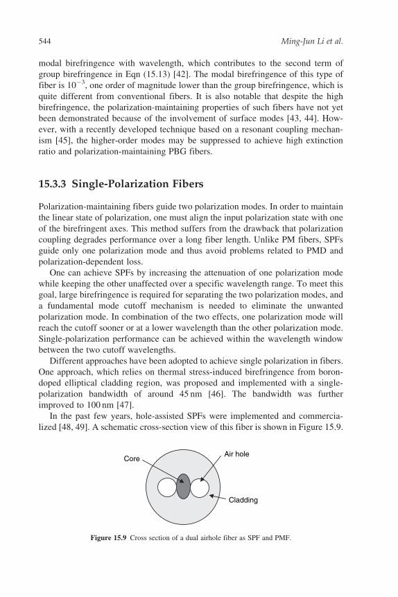
modal birefringence with wavelength, which contributes to the second term of
group birefringence in Eqn (15.13) [42]. The modal birefringence of this type of
fiber is 10�3, one order of magnitude lower than the group birefringence, which is
quite different from conventional fibers. It is also notable that despite the high
birefringence, the polarization-maintaining properties of such fibers have not yet
been demonstrated because of the involvement of surface modes [43, 44]. How-
ever, with a recently developed technique based on a resonant coupling mechan-
ism [45], the higher-order modes may be suppressed to achieve high extinction
ratio and polarization-maintaining PBG fibers.
15.3.3 Single-Polarization Fibers
Polarization-maintaining fibers guide two polarization modes. In order to maintain
the linear state of polarization, one must align the input polarization state with one
of the birefringent axes. This method suffers from the drawback that polarization
coupling degrades performance over a long fiber length. Unlike PM fibers, SPFs
guide only one polarization mode and thus avoid problems related to PMD and
polarization-dependent loss.
One can achieve SPFs by increasing the attenuation of one polarization mode
while keeping the other unaffected over a specific wavelength range. To meet this
goal, large birefringence is required for separating the two polarization modes, and
a fundamental mode cutoff mechanism is needed to eliminate the unwanted
polarization mode. In combination of the two effects, one polarization mode will
reach the cutoff sooner or at a lower wavelength than the other polarization mode.
Single-polarization performance can be achieved within the wavelength window
between the two cutoff wavelengths.
Different approaches have been adopted to achieve single polarization in fibers.
One approach, which relies on thermal stress-induced birefringence from boron-
doped elliptical cladding region, was proposed and implemented with a single-
polarization bandwidth of around 45 nm [46]. The bandwidth was further
improved to 100 nm [47].
In the past few years, hole-assisted SPFs were implemented and commercia-
lized [48, 49]. A schematic cross-section view of this fiber is shown in Figure 15.9.
CoreAir hole
Cladding
Figure 15.9 Cross section of a dual airhole fiber as SPF and PMF.
544 Ming-Jun Li et al.
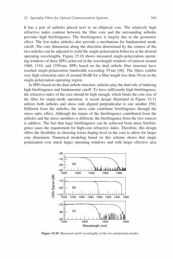
It has a pair of airholes placed next to an elliptical core. The relatively high
refractive index contrast between the fiber core and the surrounding airholes
provides high birefringence. The birefringence is largely due to the geometric
effect. The low-index airholes also provide a mechanism for fundamental mode
cutoff. The core dimension along the direction determined by the centers of the
two airholes can be adjusted to yield the single-polarization behavior at the desired
operating wavelengths. Figure 15.10 shows measured single-polarization operat-
ing windows of three SPFs achieved in the wavelength windows of interest around
1060, 1310, and 1550 nm. SPFs based on the dual airhole fiber structure have
reached single-polarization bandwidth exceeding 55 nm [48]. The fibers exhibit
very high extinction ratio of around 60 dB for a fiber length less than 30 cm in the
single-polarization operating region.
In SPFs based on the dual airhole structure, airholes play the dual role of inducing
high birefringence and fundamental cutoff. To have sufficiently high birefringence,
the refractive index of the core should be high enough, which limits the core size of
the fiber for single-mode operation. A recent design illustrated in Figure 15.11
utilizes both airholes and stress rods aligned perpendicular to one another [50].
Different from the airholes, the stress rods contribute birefringence through the
stress–optic effect. Although the nature of the birefringence contributed from the
airholes and the stress members is different, the birefringence from the two sources
is additive. The fact that large birefringence can be achieved from stress birefrin-
gence eases the requirement for high-core refractive index. Therefore, this design
offers the flexibility in choosing lower doping level in the core to allow for larger
core dimension. Numerical modeling based on this scheme shows that single
polarization over much larger operating windows and with larger effective area
Wavelength (nm)
–90
–80
–70
OS
A S
igna
l (dB
)
–110
–90
–70
–901000 1020 1040 1060 1080
1220 1240 1260 1280 1300 1320 1340 1360
1450 1500 1550 1600
–80
–70
–60
(a)
(b)
(c)
Figure 15.10 Measured cutoff wavelengths of the two polarization modes.
15. Specialty Fibers for Optical Communication Systems 545
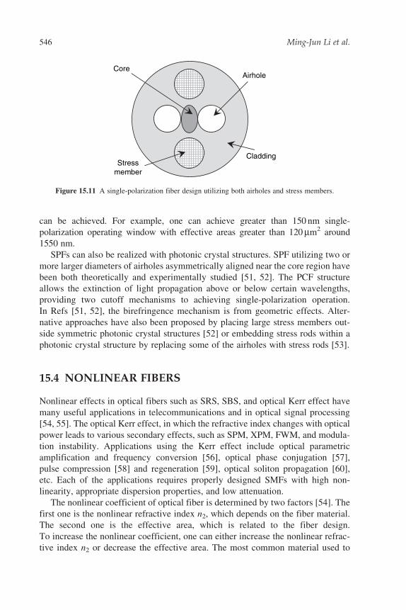
can be achieved. For example, one can achieve greater than 150 nm single-
polarization operating window with effective areas greater than 120 mm2 around
1550 nm.
SPFs can also be realized with photonic crystal structures. SPF utilizing two or
more larger diameters of airholes asymmetrically aligned near the core region have
been both theoretically and experimentally studied [51, 52]. The PCF structure
allows the extinction of light propagation above or below certain wavelengths,
providing two cutoff mechanisms to achieving single-polarization operation.
In Refs [51, 52], the birefringence mechanism is from geometric effects. Alter-
native approaches have also been proposed by placing large stress members out-
side symmetric photonic crystal structures [52] or embedding stress rods within a
photonic crystal structure by replacing some of the airholes with stress rods [53].
15.4 NONLINEAR FIBERS
Nonlinear effects in optical fibers such as SRS, SBS, and optical Kerr effect have
many useful applications in telecommunications and in optical signal processing
[54, 55]. The optical Kerr effect, in which the refractive index changes with optical
power leads to various secondary effects, such as SPM, XPM, FWM, and modula-
tion instability. Applications using the Kerr effect include optical parametric
amplification and frequency conversion [56], optical phase conjugation [57],
pulse compression [58] and regeneration [59], optical soliton propagation [60],
etc. Each of the applications requires properly designed SMFs with high non-
linearity, appropriate dispersion properties, and low attenuation.
The nonlinear coefficient of optical fiber is determined by two factors [54]. The
first one is the nonlinear refractive index n2, which depends on the fiber material.
The second one is the effective area, which is related to the fiber design.
To increase the nonlinear coefficient, one can either increase the nonlinear refrac-
tive index n2 or decrease the effective area. The most common material used to
CladdingStress
member
CoreAirhole
Figure 15.11 A single-polarization fiber design utilizing both airholes and stress members.
546 Ming-Jun Li et al.
make optical fiber is Ge-doped silica whose n2 is 3.2� 10�16 cm/W. Although
materials with n2 higher than Ge-doped silica glass exist (e.g. chalcogenide
glass), it is difficult to make an optical fiber with low loss using these materials.
For Ge-doped silica fiber, because the increase of n2 is not very significant with Ge
concentration, the main player for increasing the nonlinearity is to decrease the
effective area. However, the effective area is only one of the many fiber para-
meters that need to be considered. Other parameters such as dispersion, cutoff
wavelength, and attenuation are also important for nonlinear applications. There-
fore, an optimum nonlinear fiber design depends on the tradeoffs among the
different parameters.
This section discusses nonlinear fiber designs for applications using optical
Kerr effects.
15.4.1 Nonlinear Fiber Requirements
In designing a nonlinear fiber, several requirements need to be considered. The
first one is that the fiber needs to have high nonlinearity to achieve an efficient
nonlinear interaction. The fiber nonlinearity can be described by the nonlinear
coefficient , which is defined by [54]
=2�
�
n2
Aeff(15.18)
where n2 is the fiber nonlinear refractive index, and Aeff is the effective area of the
mode, and � is the wavelength of the light. For Ge-doped fibers, n2 does not
change significantly with Ge-doping level. Therefore, the effective area has to be
small to increase the nonlinear coefficient.
The second requirement is that the fiber needs to have low attenuation to
increase the effective interaction length, which is defined as
Leff =1� e��L
�(15.19)
where L is the fiber length. For a long fiber, Leff is approximately 1/�. Lowering
the fiber attenuation increases the effective interaction length. The four factors that
contribute to total attenuation are described by Eqn (15.8). Some of these factors
can be changed by profile designs.
If the loss due to the nonlinear scattering is not significant, it is common to use a
figure of merit to describe the nonlinear efficiency:
F0 =
�(15.20)
15. Specialty Fibers for Optical Communication Systems 547
When the pump power reaches the threshold of nonlinear scattering, the loss due to
the nonlinear scattering becomes dominant. However, in the nonlinear scattering
regime where the loss due to nonlinear scattering increases with the pump power,
the conventional figure of merit definition is no longer appropriate to describe the
nonlinear efficiency. A new figure of merit definition was introduced by taking the
pump power P0 into account:
F =P0
�=
Leff
Lnl(15.21)
Note that 1/� is the effective length and 1/P0 is the nonlinear length. The physical
meaning of the nonlinear figure of merit is that the nonlinear effect is enhanced by
increasing the effective length or decreasing the nonlinear length. Because the
threshold of SRS is normally much smaller than that of SBS, the pump power that
can be used is mainly limited by SBS. Therefore, in the nonlinear scattering
regime, the pump power loss is approximately proportional to the average gain
coefficient of SBS �gB and the pump power:
�= �gBP0 (15.22)
The figure of merit in Eqn (15.21) becomes:
F =
�gB(15.23)
This new definition is convenient to compare fibers when the SBS limits the
amount of useable power. High figure of merit means more pump power can be
used to produce the desired nonlinear effect.
The third requirement is that the fiber must have the right amount of dispersion,
which depends on the application. For example, for FWM, the dispersion needs to be
near zero to achieve the phase-matching condition. For optical soliton effects, a
certain amount of anomalous (D> 0) dispersion is required depending on the pump
power level. Furthermore, it is advantageous to design a dispersion-decreasing fiber
(DDF) to adapt the power decrease along the fiber for this type of application [61].
Another requirement is that the fiber must have low PMD. There are two ways
to reduce fiber PMD [25]. The first one is to minimize asymmetries in the index
profile and stress profile [62]. The second method for reducing fiber PMD is to
introduce controlled polarization-mode coupling by fiber spinning [24, 63].
15.4.2 Fiber Designs
Fiber profile design plays an important role in meeting the three above-mentioned
requirements. For designing a nonlinear fiber, the simplest design is the step-index
548 Ming-Jun Li et al.
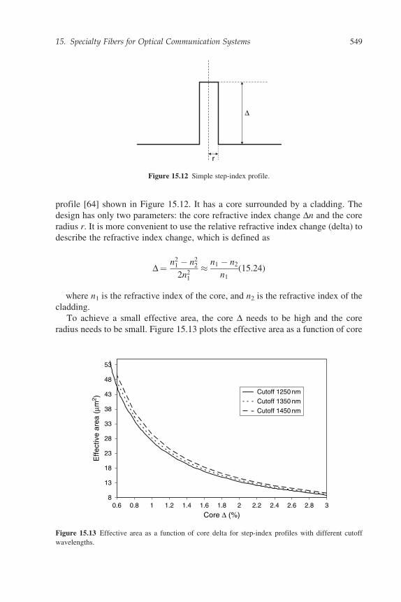
profile [64] shown in Figure 15.12. It has a core surrounded by a cladding. The
design has only two parameters: the core refractive index change Dn and the core
radius r. It is more convenient to use the relative refractive index change (delta) to
describe the refractive index change, which is defined as
D =n2
1 � n22
2n21
� n1 � n2
n1
(15.24)
where n1 is the refractive index of the core, and n2 is the refractive index of the
cladding.
To achieve a small effective area, the core D needs to be high and the core
radius needs to be small. Figure 15.13 plots the effective area as a function of core
Δ
r
Figure 15.12 Simple step-index profile.
8
13
18
23
28
33
38
43
48
53
0.6 0.8 1 1.2 1.4 1.6 1.8 2 2.2 2.4 2.6 2.8 3
Core Δ (%)
Effe
ctiv
e ar
ea (
μm2 )
Cutoff 1250 nm
Cutoff 1350 nm
Cutoff 1450 nm
Figure 15.13 Effective area as a function of core delta for step-index profiles with different cutoff
wavelengths.
15. Specialty Fibers for Optical Communication Systems 549
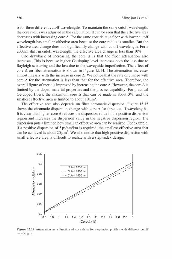
D for three different cutoff wavelengths. To maintain the same cutoff wavelength,
the core radius was adjusted in the calculation. It can be seen that the effective area
decreases with increasing core D. For the same core delta, a fiber with lower cutoff
wavelength has smaller effective area because the core radius is smaller. But the
effective area change does not significantly change with cutoff wavelength. For a
200 nm shift in cutoff wavelength, the effective area change is less than 10%.
One drawback of increasing the core D is that the fiber attenuation also
increases. This is because higher Ge-doping level increases both the loss due to
Rayleigh scattering and the loss due to the waveguide imperfection. The effect of
core D on fiber attenuation is shown in Figure 15.14. The attenuation increases
almost linearly with the increase in core D. We notice that the rate of change with
core D for the attenuation is less than that for the effective area. Therefore, the
overall figure of merit is improved by increasing the core D. However, the core D is
limited by the doped material properties and the process capability. For practical
Ge-doped fibers, the maximum core D that can be made is about 3%, and the
smallest effective area is limited to about 10 mm2.
The effective area also depends on fiber chromatic dispersion. Figure 15.15
shows the chromatic dispersion change with core D for three cutoff wavelengths.
It is clear that higher-core D reduces the dispersion value in the positive dispersion
region and increases the dispersion value in the negative dispersion region. The
dispersion puts a limit on how small an effective area can be realized. For example,
if a positive dispersion of 5 ps/nm/km is required, the smallest effective area that
can be achieved is about 20 mm2. We also notice that high positive dispersion with
small effective area is difficult to realize with a step-index design.
0.2
0.22
0.24
0.26
0.28
0.3
0.32
0.6 0.8 1 1.2 1.4 1.6 1.8 2 2.2 2.4 2.6 2.8 3
Core Δ (%)
Atte
nuat
ion
(dB
/km
) Cutoff 1250 nm
Cutoff 1350 nm
Cutoff 1450 nm
Figure 15.14 Attenuation as a function of core delta for step-index profiles with different cutoff
wavelengths.
550 Ming-Jun Li et al.
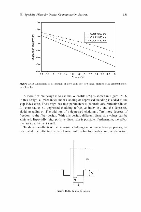
A more flexible design is to use the W-profile [65] as shown in Figure 15.16.
In this design, a lower-index inner cladding or depressed cladding is added to the
step-index core. The design has four parameters to control: core refractive index
D1, core radius r1, depressed cladding refractive index D2, and the depressed
cladding radius r2. The addition of a depressed cladding offers more degrees of
freedom to the fiber design. With this design, different dispersion values can be
achieved. Especially, high positive dispersion is possible. Furthermore, the effec-
tive area can be kept small.
To show the effects of the depressed cladding on nonlinear fiber properties, we
calculated the effective area change with refractive index in the depressed
–40
–30
–20
–10
0
10
20
30
0.6 0.8 1 1.2 1.4 1.6 1.8 2 2.2 2.4 2.6 2.8 3
Core Δ (%)
Dis
pers
ion
(ps/
nm/k
m) Cutoff 1250 nm
Cutoff 1350 nm
Cutoff 1450 nm
Figure 15.15 Dispersion as a function of core delta for step-index profiles with different cutoff
wavelengths.
Δ1
r1
r2
Δ2
Figure 15.16 W-profile design.
15. Specialty Fibers for Optical Communication Systems 551
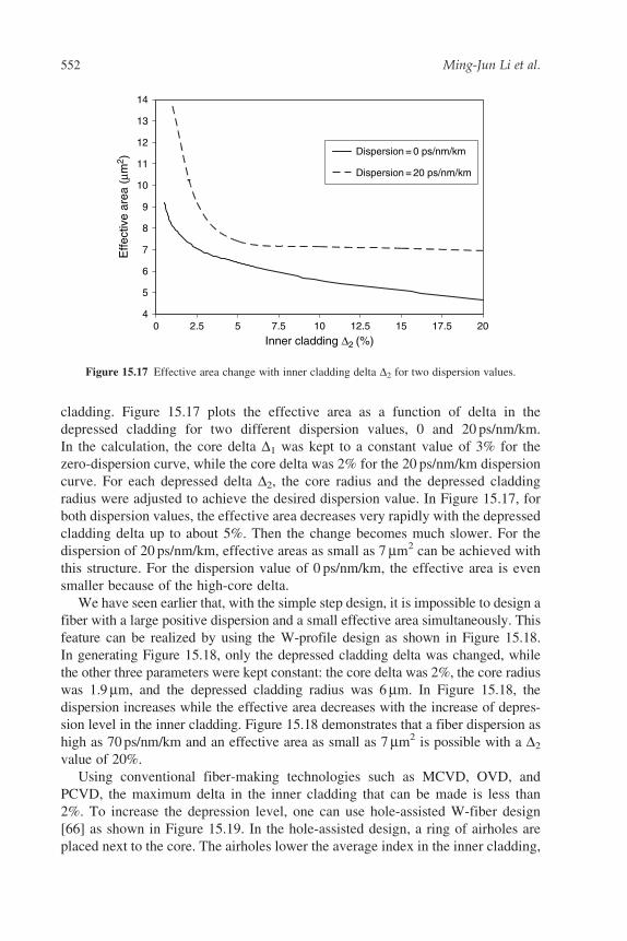
cladding. Figure 15.17 plots the effective area as a function of delta in the
depressed cladding for two different dispersion values, 0 and 20 ps/nm/km.
In the calculation, the core delta D1 was kept to a constant value of 3% for the
zero-dispersion curve, while the core delta was 2% for the 20 ps/nm/km dispersion
curve. For each depressed delta D2, the core radius and the depressed cladding
radius were adjusted to achieve the desired dispersion value. In Figure 15.17, for
both dispersion values, the effective area decreases very rapidly with the depressed
cladding delta up to about 5%. Then the change becomes much slower. For the
dispersion of 20 ps/nm/km, effective areas as small as 7 mm2 can be achieved with
this structure. For the dispersion value of 0 ps/nm/km, the effective area is even
smaller because of the high-core delta.
We have seen earlier that, with the simple step design, it is impossible to design a
fiber with a large positive dispersion and a small effective area simultaneously. This
feature can be realized by using the W-profile design as shown in Figure 15.18.
In generating Figure 15.18, only the depressed cladding delta was changed, while
the other three parameters were kept constant: the core delta was 2%, the core radius
was 1.9 mm, and the depressed cladding radius was 6 mm. In Figure 15.18, the
dispersion increases while the effective area decreases with the increase of depres-
sion level in the inner cladding. Figure 15.18 demonstrates that a fiber dispersion as
high as 70 ps/nm/km and an effective area as small as 7 mm2 is possible with a D2
value of 20%.
Using conventional fiber-making technologies such as MCVD, OVD, and
PCVD, the maximum delta in the inner cladding that can be made is less than
2%. To increase the depression level, one can use hole-assisted W-fiber design
[66] as shown in Figure 15.19. In the hole-assisted design, a ring of airholes are
placed next to the core. The airholes lower the average index in the inner cladding,
40 2.5 5 7.5 10 12.5 15 17.5 20
5
6
7
8
9
10
11
12
13
14
Inner cladding Δ2 (%)
Effe
ctiv
e ar
ea (
μm2 )
Dispersion = 0 ps/nm/km
Dispersion = 20 ps/nm/km
Figure 15.17 Effective area change with inner cladding delta D2 for two dispersion values.
552 Ming-Jun Li et al.
creating an effective depressed cladding structure. In this design, the depression
level in the inner cladding depends on the air fraction. For an average delta of
�20%, the air-fill fraction is about 65%, which can be realized in a practical hole-
assisted fiber. Using a hole-assisted design, a fiber with dispersion of 43.8 ps/nm/km
and effective area of 23 mm2 has been demonstrated [66].
For applications in optical signal processing such as adiabatic pulse compres-
sion using optical soliton effects, DDFs are desired to achieve effective amplifica-
tion through the change of the dispersion. There are two ways to make DDFs.
4
6
8
10
12
14
16
–10
0
10
20
30
40
50
60
70
80
90
Dis
pers
ion
(ps/
nm/k
m)
Aeff
Dispersion
Effe
ctiv
e ar
ea (
μm2 )
Inner cladding Δ2 (%)0 2.5 5 7.5 10 12.5 15 17.5 20
Figure 15.18 Dispersion and effective area change with inner cladding delta D2.
Cladding
Ge-doped core
Airhole
Figure 15.19 Hole-assisted W-profile design.
15. Specialty Fibers for Optical Communication Systems 553
The first one is to change the core diameter, and the second one is to change the
core delta. The core diameter can be changed easily by changing the fiber diameter
during the fiber draw process. Figure 15.20(a) shows an example of dispersion
change with the fiber diameter. The profile in Figure 15.20(a) is a W-profile with
the following parameters when the fiber diameter is 125 mm: D1 = 2%,
r1 = 1.89 mm, D2 =�0.4%, and r2 = 7 mm. By drawing the fiber diameter from
135 to 115 mm, the dispersion is decreased by about 14 ps/nm/km. Meanwhile, the
effective area is also decreased. The core delta change can be realized by changing
the dopant level in the core during the preform-making process. An example of
dispersion change with core delta is shown in Figure 15.20(b). The profile in
–6115
0.8 0.9 1 1.1 1.2 1.3 1.4 1.5 1.6 1.7 1.8
120 125 130 135
–4
–2
0
2
4
6
8
10
12
Fiber diameter (μm)
(a)
(b)
Dis
pers
ion
(ps/
nm/k
m)
Dis
pers
ion
(ps/
nm/k
m)
11
12
13
14
15
Effe
ctiv
e ar
ea (
μm2 )
Effe
ctiv
e ar
ea (
μm2 )
DispersionEffective area
DispersionEffective area
0
2
4
6
8
10
12
14
16
18
20
Core delta (%)
14
16
18
20
22
24
26
Figure 15.20 Effects of fiber diameter (a) and fiber core delta (b) on fiber dispersion and effective area.
554 Ming-Jun Li et al.
Figure 15.20(b) is also a W-profile. By reducing the core delta from 1.8 to 0.8%,
the dispersion is decreased by about 16 ps/nm/km. Unlike the case of fiber
diameter change, the effective area increases with decreasing dispersion. One
advantage of changing the core delta is that SBS effects can be reduced, while
changing the core diameter has very little impact on SBS.
15.4.3 Typical Fiber Performance
Silica-based nonlinear fibers can be manufactured by different manufacturing
processes such as OVD, MCVD, and PCVD. For nonlinear fibers made by the
OVD process, typical fiber performance is listed in Table 15.3. It can be seen that
the effective area is in the range between 15 and 25 mm2, depending on the
dispersion and dispersion slope of the fiber. Dispersion values can be controlled
from 0 to 20 ps/nm/km. Dispersion slope is less than 0.06 ps/nm2/km. Flat disper-
sion around 1550 nm can also be achieved. The cutoff wavelength is less than
1550 nm, which is suitable for applications at the 1550-nm wavelength window.
Typical attenuation is about 0.5 dB/km.
15.5 DOUBLE-CLAD FIBERS FOR FIBER LASERSAND AMPLIFIERS BY OVD
15.5.1 Introduction
The concept of double-clad fibers first emerged in the late 1980s at Polaroid
Corporation [67] as a means to boost power-scaling properties in fiber lasers and
amplifiers. Fiber lasers/amplifiers had been invented in the 1960s by Snitzer [68]
at the then American Optical, not long after the first demonstration of solid-state
lasers [69]. However, it was not until the 1980s that these fiber-based devices
began to be exploited in industrial applications. There were two key-enabling
drivers developed during that period. The first was the development of semicon-
ductor laser diode, which enabled a practical and efficient pumping mechanism for
Table 15.3
Typical properties of nonlinear fibers.
Parameter Typical value
Effective area 15–25 mm2
Dispersion 0–20 ps/nm/km
Dispersion slope 0–0.06 ps/nm2/km
Cutoff wavelength 1200–1500 nm
Attenuation 0.4–0.7 dB/km
15. Specialty Fibers for Optical Communication Systems 555
fiber-based lasers and amplifiers. The second was achievement of low-loss, rare-
earth-doped optical fiber [70] as the gain media in the fiber devices. Early work on
single-transverse-mode fiber lasers focused on devices that could be pumped with
single-mode laser diodes [71]. Then, it became apparent later in the 1980s that
scaling to higher powers was limited by the single-mode pump access. To over-
come the limitation, the group at Polaroid fabricated the first double-clad fiber,
also called “cladding-pumped fiber,” as a way to explore the use of higher power
capable, MM semiconductor laser diodes/bars to generate higher power fiber laser
devices [72]. The concept generated intense interest worldwide on the develop-
ment of practical high-power fiber laser oscillators and amplifiers with superior
beam-quality to other conventional solid-state lasers.
Attractive features of fiber lasers are many that include small footprint, light
weight, low operation/maintenance cost, minimal thermal-effect, excellent quan-
tum-efficiency and reliability, superior beam-quality (often near diffraction-
limited), flexible beam delivery, and capable of a variety of operating wavelengths
for both CW- and pulsed-mode operation. In recent years, high-power fiber lasers
have clearly emerged as a new generation of lasers. They are highly competitive
for many important industrial applications such as in material processing, biome-
dical, printing, microfabrication, military, coherent, and space communications
systems. Most typically, they compete in those applications traditionally served by
diode- or lamp-pumped solid-state YAG lasers, and potentially also in areas
covered by high-power CO2 gas lasers among others. These recognitions have
enabled fiber lasers to steadily gain ground on other laser markets, especially after
several recent impressive demonstrations of near-diffraction-limited beam quali-
ties at kilowatt output power levels from fiber laser sources [73].
New glass-composition fiber design and advanced fiber fabrication have, and
will continue, to play key roles as technological enablers for further scaling the
output power of fiber laser oscillator or amplifier with high beam quality [74]. This
section will briefly review the fundamental working principle of double-clad
optical fibers, and then introduce some newly established fiber design and fabrica-
tion method by OVD for the development of advanced double-clad optical fibers
that can mitigate, or eliminate, various detrimental nonlinear optical effects, such
as SBS, SRS, and other Kerr-type nonlinear effects in higher power applications.
15.5.2 Double-Clad Fiber 101
Different from conventional “single-clad” optical fiber, double-clad optical fiber
has a core with two cladding layers, the inner- and outer clad, as schematically
shown in Figure 15.21. The inner-clad is optically used as a “pump-core” to allow
the launched light coupling into the fiber from MM semiconductor laser diodes/
bars, while the outer clad accordingly serves as a “pump-clad” to secure the pump
guiding and coupling from the MM laser-diodes or laser-bars. Hence the reason in
the early days, these fibers were often referred to as “cladding-pumped fibers.”
556 Ming-Jun Li et al.
The pump coupling is conventionally launched through either or both fiber-end(s).
However, there are novel methods developed by pumping through the sides of
double-clad fibers [75]. The core is preferably Yb-doped in the double-clad fiber
for high-power applications. This is because the Yb3þ has a very simple
energy-level scheme as shown in Figure 15.22. It has key characteristics like low
quantum-defect (10% when pumping at 976 nm and lasing at 1080 nm), and high
quantum-yield (no ESA or upconversion transitions). Plus, Yb3þ has high absorp-
tion cross sections at 976, 940, and 915 nm (also shown in Figure 15.22), where
powerful semiconductor laser diodes or bars are readily available in hundreds of
kWs commercially. These make Yb an ideal dopant, and well suited, for high-
power applications. Other typical rare-earth dopants for active fibers include Er3þ,
Tm3þ, Nd3þ, Pr3þ, Ho3þ, Tb3þ, and Sm3þ. The doped core is preferably centered in
the fiber but having a noncircular inner-clad perimeter shape; otherwise, an off-
centered core is necessary [76] as given in Figure 15.21(a). This is to allow good
overlap of the MM pump-light with the actively doped core largely through
Core
Inner clad
Outer clad
CoreInner clad
Outer clad
(a) (b)
Figure 15.21 Schematic of double-clad optical fibers (this figure may be seen in color on the included
CD-ROM).
9002F7/2
2F5/2
910 974 1005 1040 1068 nm
102671057010990 cm–1
650
8500
500
1000
Cro
ss s
ectio
ns (
10–2
7 m2 )
1500
2000
2500
3000
900
Absorption
Emission
950
Wavelength [nm]1000 1050 1100 1150
3200
Figure 15.22 Yb3þ energy levels and spectral properties in silica.
15. Specialty Fibers for Optical Communication Systems 557
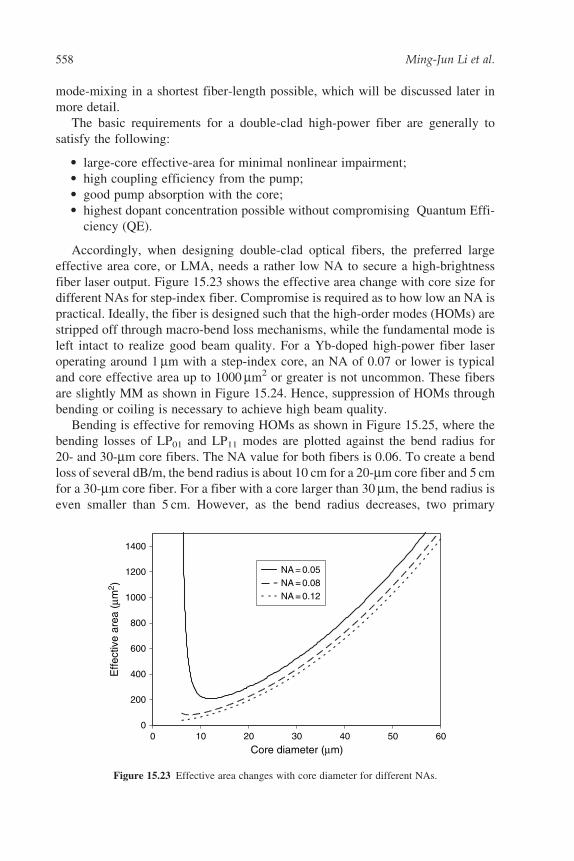
mode-mixing in a shortest fiber-length possible, which will be discussed later in
more detail.
The basic requirements for a double-clad high-power fiber are generally to
satisfy the following:
• large-core effective-area for minimal nonlinear impairment;
• high coupling efficiency from the pump;
• good pump absorption with the core;
• highest dopant concentration possible without compromising Quantum Effi-
ciency (QE).
Accordingly, when designing double-clad optical fibers, the preferred large
effective area core, or LMA, needs a rather low NA to secure a high-brightness
fiber laser output. Figure 15.23 shows the effective area change with core size for
different NAs for step-index fiber. Compromise is required as to how low an NA is
practical. Ideally, the fiber is designed such that the high-order modes (HOMs) are
stripped off through macro-bend loss mechanisms, while the fundamental mode is
left intact to realize good beam quality. For a Yb-doped high-power fiber laser
operating around 1 mm with a step-index core, an NA of 0.07 or lower is typical
and core effective area up to 1000 mm2 or greater is not uncommon. These fibers
are slightly MM as shown in Figure 15.24. Hence, suppression of HOMs through
bending or coiling is necessary to achieve high beam quality.
Bending is effective for removing HOMs as shown in Figure 15.25, where the
bending losses of LP01 and LP11 modes are plotted against the bend radius for
20- and 30-mm core fibers. The NA value for both fibers is 0.06. To create a bend
loss of several dB/m, the bend radius is about 10 cm for a 20-mm core fiber and 5 cm
for a 30-mm core fiber. For a fiber with a core larger than 30 mm, the bend radius is
even smaller than 5 cm. However, as the bend radius decreases, two primary
00 10 20 30 40 50 60
200
400
600
800
1000
1200
1400
Core diameter (μm)
Effe
ctiv
e ar
ea (
μm2 )
NA = 0.05NA = 0.08NA = 0.12
Figure 15.23 Effective area changes with core diameter for different NAs.
558 Ming-Jun Li et al.
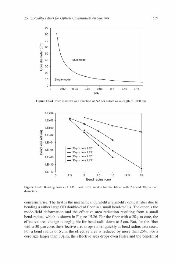
concerns arise. The first is the mechanical durability/reliability optical fiber due to
bending a rather large OD double-clad fiber in a small bend-radius. The other is the
mode-field deformation and the effective area reduction resulting from a small
bend-radius, which is shown in Figure 15.26. For the fiber with a 20-mm core, the
effective area change is negligible for bend-radii down to 5 cm. But, for the fiber
with a 30-mm core, the effective area drops rather quickly as bend radius decreases.
For a bend radius of 5 cm, the effective area is reduced by more than 25%. For a
core size larger than 30 mm, the effective area drops even faster and the benefit of
Single mode
Multimode
00 0.02 0.04 0.06 0.08 0.1 0.12 0.14
10
20
30
40
50
60
70
80
90
NA
Cor
e di
amet
er (
μm)
Figure 15.24 Core diameter as a function of NA for cutoff wavelength of 1060 nm.
1.E–120 2.5 5 7.5 10 12.5 15
1.E–10
1.E–08
1.E–06
1.E–04
1.E–02
1.E+00
1.E+02
1.E+04
Bend radius (cm)
Ben
d lo
ss (
dB/m
)
20 μm core LP0120 μm core LP1130 μm core LP0130 μm core LP11
Figure 15.25 Bending losses of LP01 and LP11 modes for the fibers with 20- and 30-mm core
diameters.
15. Specialty Fibers for Optical Communication Systems 559
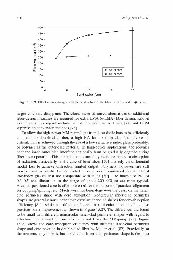
larger core size disappears. Therefore, more advanced alternatives or additional
fiber-design measures are required for extra LMA (e-LMA) fiber design. Known
examples in this regard include helical-core double-clad fibers [77] and HOM
suppression/conversion methods [78].
To allow the high-power MM pump light from laser diode bars to be efficiently
coupled into double-clad fiber, a high NA for the inner-clad “pump-core” is
critical. This is achieved through the use of a low-refractive-index glass preferably,
or polymer as the outer-clad material. In high-power applications, the polymer
near the inner–outer clad interface can easily burn or gradually degrade during
fiber laser operation. This degradation is caused by moisture, stress, or absorption
of radiation, particularly in the case of bent fibers [79] that rely on differential
modal loss to achieve diffraction-limited output. Polymers, however, are still
mostly used in reality due to limited or very poor commercial availability of
low-index glasses that are compatible with silica [80]. The inner-clad NA of
0.3–0.5 and dimension in the range of about 200–450 mm are most typical.
A center-positioned core is often preferred for the purpose of practical alignment
for coupling/splicing, etc. Much work has been done over the years on the inner-
clad perimeter shape with core absorption. Noncircular inner-clad perimeter
shapes are generally much better than circular inner-clad shapes for core-absorption
efficiency [81], while an off-centered core in a circular inner cladding also
provides some improvement as shown in Figure 15.27. The differences are found
to be small with different noncircular inner-clad perimeter shapes with regard to
effective core absorption similarly launched from the MM-pump [82]. Figure
15.27 shows the core-absorption efficiency with different inner-clad perimeter
shape and core position in double-clad fiber by Muller et al. [82]. Practically, at
the moment, a symmetric but noncircular inner-clad perimeter shape is the most
00 5 10 15 20
50
100
150
200
250
300
350
400
450
500
Bend radius (cm)
Effe
ctiv
e ar
ea (
μm2 )
20 μm core30 μm core
Figure 15.26 Effective area changes with the bend radius for the fibers with 20- and 30-mm core.
560 Ming-Jun Li et al.
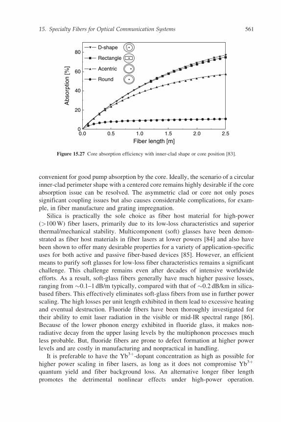
convenient for good pump absorption by the core. Ideally, the scenario of a circular
inner-clad perimeter shape with a centered core remains highly desirable if the core
absorption issue can be resolved. The asymmetric clad or core not only poses
significant coupling issues but also causes considerable complications, for exam-
ple, in fiber manufacture and grating impregnation.
Silica is practically the sole choice as fiber host material for high-power
(>100 W) fiber lasers, primarily due to its low-loss characteristics and superior
thermal/mechanical stability. Multicomponent (soft) glasses have been demon-
strated as fiber host materials in fiber lasers at lower powers [84] and also have
been shown to offer many desirable properties for a variety of application-specific
uses for both active and passive fiber-based devices [85]. However, an efficient
means to purify soft glasses for low-loss fiber characteristics remains a significant
challenge. This challenge remains even after decades of intensive worldwide
efforts. As a result, soft-glass fibers generally have much higher passive losses,
ranging from 0.1–1 dB/m typically, compared with that of 0.2 dB/km in silica-
based fibers. This effectively eliminates soft-glass fibers from use in further power
scaling. The high losses per unit length exhibited in them lead to excessive heating
and eventual destruction. Fluoride fibers have been thoroughly investigated for
their ability to emit laser radiation in the visible or mid-IR spectral range [86].
Because of the lower phonon energy exhibited in fluoride glass, it makes non-
radiative decay from the upper lasing levels by the multiphonon processes much
less probable. But, fluoride fibers are prone to defect formation at higher power
levels and are costly in manufacturing and nonpractical in handling.
It is preferable to have the Yb3þ-dopant concentration as high as possible for
higher power scaling in fiber lasers, as long as it does not compromise Yb3þ
quantum yield and fiber background loss. An alternative longer fiber length
promotes the detrimental nonlinear effects under high-power operation.
Fiber length [m]
D-shape
Rectangle
Acentric
Round
80
60
40
20
00.0 0.5 1.0 1.5 2.0 2.5
Abs
orpt
ion
[%]
Figure 15.27 Core absorption efficiency with inner-clad shape or core position [83].
15. Specialty Fibers for Optical Communication Systems 561
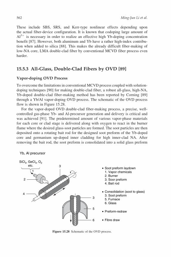
These include SBS, SRS, and Kerr-type nonlinear effects depending upon
the actual fiber-device configuration. It is known that codoping large amount of
Al3þ is necessary in order to realize an effective high Yb-doping concentration
benefit [87]. However, both aluminum and Yb have a rather high-index contribu-
tion when added to silica [88]. This makes the already difficult fiber-making of
low-NA core, LMA double-clad fiber by conventional MCVD fiber process even
harder.
15.5.3 All-Glass, Double-Clad Fibers by OVD [89]
Vapor-doping OVD Process
To overcome the limitations in conventional MCVD process coupled with solution-
doping techniques [90] for making double-clad fiber, a robust all-glass, high-NA,
Yb-doped double-clad fiber-making method has been reported by Corning [89]
through a Yb/Al vapor-doping OVD process. The schematic of the OVD process
flow is shown in Figure 15.28.
For the vapor-doped OVD double-clad fiber-making process, a precise, well-
controlled gas-phase Yb- and Al-precursor generation and delivery is critical and
was achieved [91]. The predetermined amount of various vapor-phase materials
for each core or clad stage is delivered along with oxygen to react in the burner
flame where the desired glass-soot particles are formed. The soot particles are then
deposited onto a rotating bait rod for the designed soot preform of the Yb-doped
core and germanium up-doped inner cladding for high inner-clad NA. After
removing the bait rod, the soot preform is consolidated into a solid glass preform
Yb, Al precursor
SiCl4, GeCl4, O2etc.
1
2
4
3Soot preform laydown1. Vapor chemicals2. Burner3. Soor preform4. Bait rod
•
• Consolidation (soot to glass)3. Soot preform5. Furnace6. Glass
• Preform-redraw
• Fibre draw
3
5
6
Figure 15.28 Schematic of the OVD process.
562 Ming-Jun Li et al.
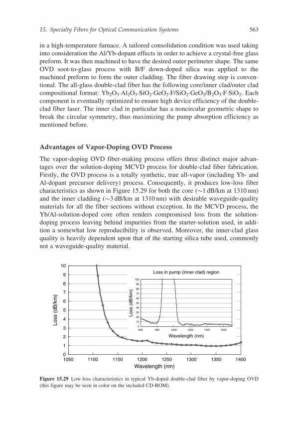
in a high-temperature furnace. A tailored consolidation condition was used taking
into consideration the Al/Yb-dopant effects in order to achieve a crystal-free glass
preform. It was then machined to have the desired outer perimeter shape. The same
OVD soot-to-glass process with B/F down-doped silica was applied to the
machined preform to form the outer cladding. The fiber drawing step is conven-
tional. The all-glass double-clad fiber has the following core/inner clad/outer clad
compositional format: Yb2O3�Al2O3�SiO2�GeO2�F/SiO2�GeO2/B2O3�F�SiO2. Each
component is eventually optimized to ensure high device efficiency of the double-
clad fiber laser. The inner clad in particular has a noncircular geometric shape to
break the circular symmetry, thus maximizing the pump absorption efficiency as
mentioned before.
Advantages of Vapor-Doping OVD Process
The vapor-doping OVD fiber-making process offers three distinct major advan-
tages over the solution-doping MCVD process for double-clad fiber fabrication.
Firstly, the OVD process is a totally synthetic, true all-vapor (including Yb- and
Al-dopant precursor delivery) process. Consequently, it produces low-loss fiber
characteristics as shown in Figure 15.29 for both the core (1 dB/km at 1310 nm)
and the inner cladding (3 dB/km at 1310 nm) with desirable waveguide-quality
materials for all the fiber sections without exception. In the MCVD process, the
Yb/Al-solution-doped core often renders compromised loss from the solution-
doping process leaving behind impurities from the starter-solution used, in addi-
tion a somewhat low reproducibility is observed. Moreover, the inner-clad glass
quality is heavily dependent upon that of the starting silica tube used, commonly
not a waveguide-quality material.
0
1
2
3
4
5
6
7
8
9
10
1050
Wavelength (nm)
Loss
(dB
/km
)
1100 1150 1200 1250 1300 1350 1400
0
10
20
30
40
50
60
70
80
90
100
600 800 1000 1200 1400 1600
Loss in pump (inner clad) region
Wavelength (nm)
Loss
(dB
/km
)
Figure 15.29 Low-loss characteristics in typical Yb-doped double-clad fiber by vapor-doping OVD
(this figure may be seen in color on the included CD-ROM).
15. Specialty Fibers for Optical Communication Systems 563
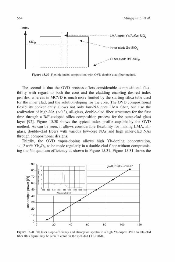
The second is that the OVD process offers considerable compositional flex-
ibility with regard to both the core and the cladding enabling desired index
profiles, whereas in MCVD is much more limited by the starting silica tube used
for the inner clad, and the solution-doping for the core. The OVD compositional
flexibility conveniently allows not only low-NA core LMA fiber, but also the
realization of high-NA (>0.3), all-glass, double-clad fiber structures for the first
time through a B/F-codoped silica composition process for the outer-clad glass
layer [92]. Figure 15.30 shows the typical index profile capable by the OVD
method. As can be seen, it allows considerable flexibility for making LMA, all-
glass, double-clad fibers with various low-core NAs and high inner-clad NAs
through compositional designs.
Thirdly, the OVD vapor-doping allows high Yb-doping concentration,
1.2 wt% Yb2O3, to be made regularly in a double-clad fiber without compromis-
ing the Yb quantum-efficiency as shown in Figure 15.31. Figure 15.31 shows the
SiO2
LMA core: Yb/Al/Ge-SiO2
Inner clad: Ge-SiO2
Outer clad: B/F-SiO2
Index
Figure 15.30 Flexible index composition with OVD double-clad fiber method.
90
80
70
60
50
Lase
r ou
tput
pow
er [W
]
40
30
20
10
00 20 40 60 80 100 120
y = 0.8198 × –7.547710
8
6
4
2
0900 920 940 960 980
Wavelength (nm)
Atte
nuat
ion
(dB
/m)
1000 1020 1040 1060
Figure 15.31 Yb laser slope-efficiency and absorption spectra in a high Yb-doped OVD double-clad
fiber (this figure may be seen in color on the included CD-ROM).
564 Ming-Jun Li et al.
Yb3þ absorption spectra measured for power launched through the MM inner-clad
pump region (insert in the figure) and the laser-slope efficiency. The fiber has a
30-mm/350-mm core/inner-clad ratio, and the doped core has 1.2 wt% Yb2O3.
The Yb peak absorption of about 8 dB/m at 976 nm, is the highest to date, to our
knowledge, with an uncompromised Yb3þ laser slope-efficiency of 82%.
15.5.4 High-Performance Yb-Doped Double-Clad Fibers
Introduction
In this section, we give an example of using the above-described “vapor-doping
OVD” process to the development of a high-performance Yb-doped double-clad
fiber, which mitigates detrimental nonlinear SBS. As fiber laser technology con-
tinues to progress with higher power output into the kilowatt range and beyond
[93], one important way to further high-power scaling is through coherent beam-
combining technology for 10s and 100s of kWs. Fiber lasers suitable for such
applications require not only high power and good beam-quality but also narrow
linewidth. High-power, narrow-linewidth fiber lasers are generally achieved by
using a master-oscillator-power-amplifier (MOPA) configuration. Typical fiber
cavity lengths of several meters make the discrimination of closely spaced long-
itudinal modes difficult in fiber lasers. The narrow-linewidth requirement of the
fiber MOPA means that SBS must be effectively managed for high-power opera-
tion, as it becomes the limiting factor in the maximal power achievable. SBS in a
fiber laser can be dealt with through geometric [94]/compositional effect(s) in the
fiber profile design and/or through the distributed temperature [95] and/or stress/
strain [96] effect(s) in the fiber laser-packaging design. Either way, raising the
SBS threshold in a high-power fiber laser represents a considerable challenge.
SBS Effect in Optical Fiber
The origin of SBS lies in the backscattering of light by acoustic waves generated in
the fiber material through the electrostrictive effect [97]. This backscattered light
has a characteristically narrow linewidth (50 MHz in silica) and is down-shifted
in frequency by the Brillouin shift, which depends on the fiber material [98]. For
common silica-based fibers, the shift is about 11 GHz at 1.55 mm (the third
telecomm window) and about 16 GHz at 1 mm (the Yb-fiber laser wavelength).
The narrow linewidth aspect of SBS makes it particularly harmful for narrow-
linewidth high-power fiber laser operation. The backscattered light in a fiber
interferes with the signal light and reinforces the density grating formed by the
electrostrictive effect. This reinforced grating then stimulates more of the forward
signal light to be backscattered. When the gain of the backscattered light is greater
than the losses due to fiber attenuation we reach the SBS-threshold, after which the
amount of backscattered light increases very rapidly with increasing input power
until nearly all the input power is reflected. The transmitted power at the fiber output
15. Specialty Fibers for Optical Communication Systems 565
saturates at a level that barely increases with increasing input power. For SMF
of lengths about 10 km, the SBS threshold can lie in the range of 8–10 dBm.
In general, larger core size, shorter fiber length, higher signal light frequency, and
broader signal linewidth all help to raise the nonlinear SBS threshold [99].
A thorough and comprehensive analysis of the SBS threshold was conducted
[100] recently with regard to the fiber-related parameters. An expression for the
threshold in terms of fiber and material parameters was derived, yielding
Pth /KAeff�u
gð�maxÞLeff�Iao
u
, (15.25)
where g(�max) is the effective gain coefficient at peak frequency, �u is the acoustic
attenuation coefficient for the acoustic mode of order u, Aeff is the optical effective
area, K is the polarization factor, Leff is the effective interaction length, and �Iaou is
the normalized overlap integral between the optic and acoustic modes. The above
equation indicates that the SBS threshold can be increased by increasing the
effective area, polarization factor, and acoustic loss or by decreasing the overlap
integral and the maximum gain coefficient. Among all the factors that affect SBS,
the effective area and overlap integral can be controlled by fiber refractive index
profile design and acoustic velocity profile design. The acoustic loss can be
controlled by glass composition. The gain coefficient can also be lowered by
creating an axially nonuniform Brillouin gain spectrum through distributed glass
dopant or stress concentrations along the fiber. And, finally, the polarization factor
can be increased through polarization control.
SBS-Managed Fiber Composition Design
As seen from Eqn (15.25), one way to raise the SBS threshold is by increasing the
optical effective area, Aeff. Indeed, this was how the now well-known LMA fiber
design concept initially came about [94]. As a matter of fact, the LMA core
increases the power thresholds for all nonlinear effects such as SRS, SBS, and
all optical Kerr-type effects in the fiber. This is simply because of the geometri-
cally reduced power density in such core design.
By taking the double-clad fiber requirement into account, we have also con-
sidered feasible compositional means to reduce SBS.
Table 15.4 lists the dopants that can be used for making silica-based fibers and
their effects on relevant optical and acoustic properties [101]. Among all the
dopants listed, alumina remarkably, is the only dopant known that lowers
the acoustic index in silica. It has been well known that boron and fluorine are
the only dopants lowering the optical index in silica. The nature and mechanism as
to why/how the addition of alumina lowers the acoustic index in silica, while
nothing else does, is an extremely complex phenomenon.
Two compositional approaches can be used for reducing the SBS effect. One
method is to design a fiber structure using different dopants that guides the optical
566 Ming-Jun Li et al.
wave but antiguides the acoustic wave. This is accomplished, for example, by
choosing a dopant in the core such as Al2O3 to increase the optical index but decrease
the acoustic index [102] or by choosing a dopant in the cladding such as F to decrease
the optical index but increase the acoustic index [103]. The resulting optical and
acoustic refractive index profiles are shown schematically in Figure 15.32(a).
Because the acoustic wave is not guided in the core region, the interaction between
the optical and the acoustic waves is reduced. Increased SBS threshold using this
approach has been experimentally demonstrated [102, 103].
The second approach to suppressing SBS effects is to use different dopants
within the core by changing the optical and acoustic field distribution to reduce the
overlap-integral, �Iaou between the optical and the acoustic field as indicated from
the Eqn (15.25). This overlap effect is ignored in conventional SBS theory [104].
For an SMF with a step-index profile made using a single dopant, this overlap
integral is approximately unity. Thus, ignoring this factor does not affect the SBS
evaluation. For all other cases however, this overlap term can be significantly
smaller than unity and cannot be neglected as demonstrated in Ref. [100]. An
example of two doping regions in the core is shown in Figure 15.32(b). In this
case, the first core region is doped with GeO2 and the second core region is doped
with Al2O3. The optical refractive index profile is selected to be a step, but the
acoustic index profile becomes a W-shape. The optical field is confined in both the
core regions while the acoustic field is confined in the first core region only. As a
result, the overlap integral is reduced significantly. Numerical modeling indicates
that the SBS threshold increase of 3–6 dB is possible using this approach.
Table 15.4
Effect on optical and acoustic properties of various dopants in silica.
Dopant GeO2 P2O5 TiO2 B2O3 F Al2O3
Optical refractive index " " " # # "Acoustic refractive index " " " " " #
Optical
Acoustic
Al2O3doped
(a) (b)
Al2O3doped GeO2
doped
Figure 15.32 Optical and acoustic profiles in fiber design.
15. Specialty Fibers for Optical Communication Systems 567
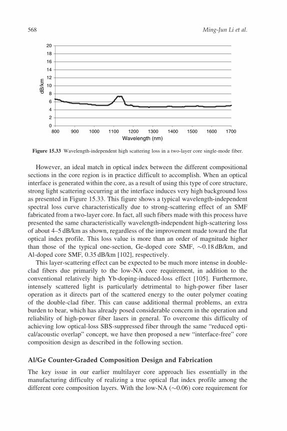
However, an ideal match in optical index between the different compositional
sections in the core region is in practice difficult to accomplish. When an optical
interface is generated within the core, as a result of using this type of core structure,
strong light scattering occurring at the interface induces very high background loss
as presented in Figure 15.33. This figure shows a typical wavelength-independent
spectral loss curve characteristically due to strong-scattering effect of an SMF
fabricated from a two-layer core. In fact, all such fibers made with this process have
presented the same characteristically wavelength-independent high-scattering loss
of about 4–5 dB/km as shown, regardless of the improvement made toward the flat
optical index profile. This loss value is more than an order of magnitude higher
than those of the typical one-section, Ge-doped core SMF, 0.18 dB/km, and
Al-doped core SMF, 0.35 dB/km [102], respectively.
This layer-scattering effect can be expected to be much more intense in double-
clad fibers due primarily to the low-NA core requirement, in addition to the
conventional relatively high Yb-doping-induced-loss effect [105]. Furthermore,
intensely scattered light is particularly detrimental to high-power fiber laser
operation as it directs part of the scattered energy to the outer polymer coating
of the double-clad fiber. This can cause additional thermal problems, an extra
burden to bear, which has already posed considerable concern in the operation and
reliability of high-power fiber lasers in general. To overcome this difficulty of
achieving low optical-loss SBS-suppressed fiber through the same “reduced opti-
cal/acoustic overlap” concept, we have then proposed a new “interface-free” core
composition design as described in the following section.
Al/Ge Counter-Graded Composition Design and Fabrication
The key issue in our earlier multilayer core approach lies essentially in the
manufacturing difficulty of realizing a true optical flat index profile among the
different core composition layers. With the low-NA (0.06) core requirement for
0800 900 1000 1100 1200 1300 1400 1500 1600 1700
2
4
6
8
10
12
14
16
18
20
Wavelength (nm)
dB/k
m
Figure 15.33 Wavelength-independent high scattering loss in a two-layer core single-mode fiber.
568 Ming-Jun Li et al.
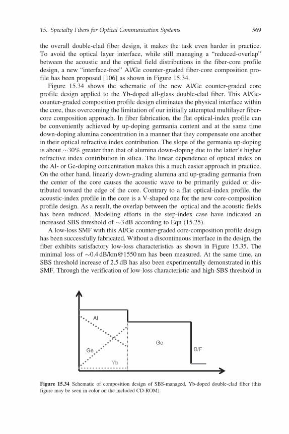
the overall double-clad fiber design, it makes the task even harder in practice.
To avoid the optical layer interface, while still managing a “reduced-overlap”
between the acoustic and the optical field distributions in the fiber-core profile
design, a new “interface-free” Al/Ge counter-graded fiber-core composition pro-
file has been proposed [106] as shown in Figure 15.34.
Figure 15.34 shows the schematic of the new Al/Ge counter-graded core
profile design applied to the Yb-doped all-glass double-clad fiber. This Al/Ge-
counter-graded composition profile design eliminates the physical interface within
the core, thus overcoming the limitation of our initially attempted multilayer fiber-
core composition approach. In fiber fabrication, the flat optical-index profile can
be conveniently achieved by up-doping germania content and at the same time
down-doping alumina concentration in a manner that they compensate one another
in their optical refractive index contribution. The slope of the germania up-doping
is about 30% greater than that of alumina down-doping due to the latter’s higher
refractive index contribution in silica. The linear dependence of optical index on
the Al- or Ge-doping concentration makes this a much easier approach in practice.
On the other hand, linearly down-grading alumina and up-grading germania from
the center of the core causes the acoustic wave to be primarily guided or dis-
tributed toward the edge of the core. Contrary to a flat optical-index profile, the
acoustic-index profile in the core is a V-shaped one for the new core-composition
profile design. As a result, the overlap between the optical and the acoustic fields
has been reduced. Modeling efforts in the step-index case have indicated an
increased SBS threshold of 3 dB according to Eqn (15.25).
A low-loss SMF with this Al/Ge counter-graded core-composition profile design
has been successfully fabricated. Without a discontinuous interface in the design, the
fiber exhibits satisfactory low-loss characteristics as shown in Figure 15.35. The
minimal loss of 0.4 dB/km@1550 nm has been measured. At the same time, an
SBS threshold increase of 2.5 dB has also been experimentally demonstrated in this
SMF. Through the verification of low-loss characteristic and high-SBS threshold in
Al
Ge
GeB/F
Yb
Figure 15.34 Schematic of composition design of SBS-managed, Yb-doped double-clad fiber (this
figure may be seen in color on the included CD-ROM).
15. Specialty Fibers for Optical Communication Systems 569
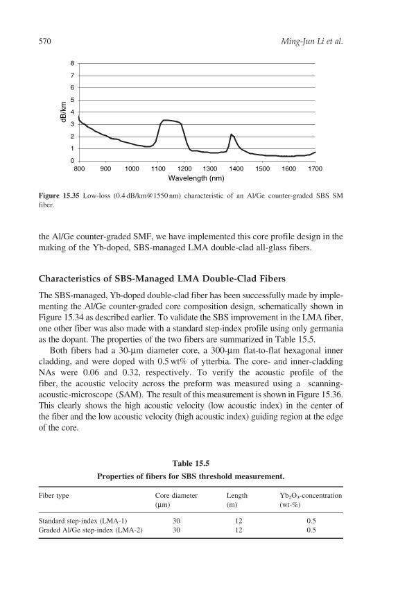
the Al/Ge counter-graded SMF, we have implemented this core profile design in the
making of the Yb-doped, SBS-managed LMA double-clad all-glass fibers.
Characteristics of SBS-Managed LMA Double-Clad Fibers
The SBS-managed, Yb-doped double-clad fiber has been successfully made by imple-
menting the Al/Ge counter-graded core composition design, schematically shown in
Figure 15.34 as described earlier. To validate the SBS improvement in the LMA fiber,
one other fiber was also made with a standard step-index profile using only germania
as the dopant. The properties of the two fibers are summarized in Table 15.5.
Both fibers had a 30-mm diameter core, a 300-mm flat-to-flat hexagonal inner
cladding, and were doped with 0.5 wt% of ytterbia. The core- and inner-cladding
NAs were 0.06 and 0.32, respectively. To verify the acoustic profile of the
fiber, the acoustic velocity across the preform was measured using a scanning-
acoustic-microscope (SAM). The result of this measurement is shown in Figure 15.36.
This clearly shows the high acoustic velocity (low acoustic index) in the center of
the fiber and the low acoustic velocity (high acoustic index) guiding region at the edge
of the core.
Table 15.5
Properties of fibers for SBS threshold measurement.
Fiber type Core diameter
(mm)
Length
(m)
Yb2O3-concentration
(wt-%)
Standard step-index (LMA-1) 30 12 0.5
Graded Al/Ge step-index (LMA-2) 30 12 0.5
0800 900 1000 1100 1200 1300 1400 1500 1600 1700
1
2
3
4
5
6
7
8
Wavelength (nm)
dB/k
m
Figure 15.35 Low-loss (0.4 dB/km@1550 nm) characteristic of an Al/Ge counter-graded SBS SM
fiber.
570 Ming-Jun Li et al.
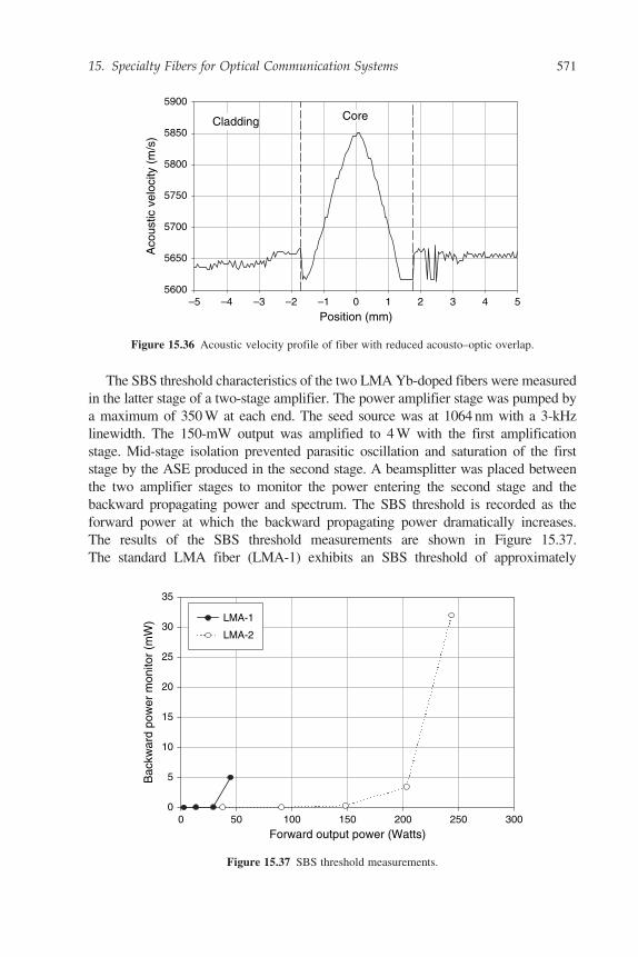
The SBS threshold characteristics of the two LMA Yb-doped fibers were measured
in the latter stage of a two-stage amplifier. The power amplifier stage was pumped by
a maximum of 350 W at each end. The seed source was at 1064 nm with a 3-kHz
linewidth. The 150-mW output was amplified to 4 W with the first amplification
stage. Mid-stage isolation prevented parasitic oscillation and saturation of the first
stage by the ASE produced in the second stage. A beamsplitter was placed between
the two amplifier stages to monitor the power entering the second stage and the
backward propagating power and spectrum. The SBS threshold is recorded as the
forward power at which the backward propagating power dramatically increases.
The results of the SBS threshold measurements are shown in Figure 15.37.
The standard LMA fiber (LMA-1) exhibits an SBS threshold of approximately
Position (mm)
Aco
ustic
vel
ocity
(m
/s)
5600–5 –4 –3 –2 –1 0 1 2 3 4 5
5650
5700
5750
5800
5850
5900
Cladding Core
Figure 15.36 Acoustic velocity profile of fiber with reduced acousto–optic overlap.
Forward output power (Watts)
Bac
kwar
d po
wer
mon
itor
(mW
)
00 50 100 150 200 250 300
5
10
15
20
25
30
35
LMA-1
LMA-2
Figure 15.37 SBS threshold measurements.
15. Specialty Fibers for Optical Communication Systems 571
40 W while the fiber with reduced acousto-optic overlap (LMA-2) showed a threshold
of between 150 and 200 W. This measurement clearly demonstrates the feasibility of
raising the SBS threshold through dopant profiling in the core of the fiber. Further-
more with the LMA-2 fiber, a fiber laser slope efficiency of over 80% has been
measured, demonstrating that such profiling provides uncompromised laser perfor-
mance. Record high-power, narrow-linewidth fiber amplifiers have also been demon-
strated with this SBS-managed fiber design, and the details are given in Ref. [107].
15.5.5 Conclusions
Vapor-doping, all-glass, double-clad fiber processes have been established through
the OVD method. The major benefits of such processes include ultralow loss, high
Yb-doping concentration, and compositional flexibility. Experimental realization
of double-clad fibers from this process provide superior power scaling and hand-
ling reliability for practical use due to its all-glass structure. Using OVD fiber-
making advantages, recent work on the composition, design, and fabrication of
SBS-managed, LMA-2 double-clad fiber lasers have been described. An alumi-
num/germanium (Al/Ge) counter-graded fiber-core composition profile has been
proposed and demonstrated as a practical means for reducing the nonlinear SBS
effect, through the reduced overlap between optical and acoustic fields in the fiber.
Such Al/Ge counter-graded composition-profile designs overcome the limitation
of multilayer fiber-core compositional approach in low-loss fiber fabrication. The
new compositionally SBS-managed, LMA-2 Yb-doped double-clad fiber laser has
been demonstrated with low-loss characteristics and high laser efficiency.
15.6 MICROSTRUCTURED OPTICAL FIBERS
15.6.1 Introduction
Microstructured optical fibers represent a new class of optical fibers that has
reinvigorated the field of specialty fibers and has redefined our understanding of
optical waveguides. As with any new advance, we can see precursors of the
technology dating back for decades before reaching a critical mass that defined
the field in its own right. In the case of microstructured fibers, the early roots of the
technology are in evidence in the holey fibers of Kaiser et al. in 1974 [108], in the
Bragg fibers from CalTech in 1978 [109], and even in the segmented core designs
of dispersion-compensating fiber and NZDSF fibers of the late 1980s and 1990s.
The turning point in the technology came in the early 1990s with the development
of the formal ideas surrounding the PBGs produced by materials with periodic
variations of refractive index [110]. It was at this time that a new class of optical
fiber was proposed based on photonic crystal effects [111], but the decade would
nearly end before a true PCF would be realized [112].
572 Ming-Jun Li et al.
The scope of microstructured fibers is very large and cannot be covered in its
entirety in this article. Rather than surveying the myriad structures and applica-
tions, we choose to focus on air/silica-microstructured fibers to convey the general
principles and most important applications of this technology. We begin with a
discussion of the fundamental principles behind waveguiding in these unusual
waveguides and then follow with more detailed discussions of the properties of
the two natural categories of microstructured optical fibers: effective index-
microstructured optical fibers (EI-MOFs) and photonic band-gap fibers (PBGFs)
as illustrated in Figure 15.38.
15.6.2 Waveguiding in Microstructured Optical Fibers
Until the introduction of photonic crystals it was generally accepted that wave-
guides required total internal reflection (TIR) to define guided optical modes.
Incomplete reflections such as those provided by metallic or dielectric surfaces
can define relatively low-loss cavities but true modes of conventional waveguides
require a high-index core that produces TIR at the core/cladding interface. This is
of course a simplified explanation motivated by a ray picture of guiding light, but
it is a conceptual picture that has had a powerful influence on the way we under-
stand waveguides. A deeper explanation of the physics behind waveguiding
ultimately resorts to a full application of Maxwell’s equations in which the rays
are replaced by electromagnetic waves, and the index profile takes on the role of a
potential. It is from this more complete electromagnetic description that the
concepts of photonic crystals and PBGs take form, ultimately leading to a broader
understanding of the requirements to observe optical waveguiding.
As we have described it, a conventional waveguide requires a high index core
surrounded by a lower index cladding that is considered to extend to infinity.
(a) (b)
Figure 15.38 Representative geometries for the two major class of air-silica microstructured optical
fibers: (a) EI-MOF and (b) PBGF. The dark areas represent airholes or voids and the light areas
represent solid glass or other optically transparent material.
15. Specialty Fibers for Optical Communication Systems 573
In reality, many conventional waveguides and optical fibers have complex core
geometries that may contain regions with refractive indices lower than that of
the cladding, making it difficult to explain the waveguide in terms of TIR at a
single interface. In anticipation of the PBG discussion, we approach conventional
waveguiding from a different direction using concepts borrowed from photonic
crystals [113].
An important yet often unappreciated result is that a homogenous material such
as a block of glass has a region of frequencies for which propagation is forbidden.
To understand this, we examine the relationship between the optical frequency !and the propagation constant � of the optical field. In a homogeneous material of
refractive index n1, a propagating solution with a propagation constant � must
have a frequency greater than �c/n1. If the frequency is less than this value, the
optical field decays and fails to propagate. This then defines a range of forbidden
frequencies from zero to �c/n1. If the refractive index is increased to n2, the
forbidden gap is smaller going from zero to �c/n2, and frequencies between
�c/n2 and �c/n1 that are forbidden in the region of refractive index n1 are now
allowed in the region of refractive index n2. Thus, an embedded high-index region
supports propagation for a range of frequencies at which propagation with propa-
gation constant � is forbidden in the lower-index cladding. This is the basic
principle behind conventional waveguides.
The above explanation still relies on two distinct macroscopic regions with a
well-defined single interface. But the concept of forbidden frequencies is a general
one, and even for more complicated waveguide geometries, there is still a well-
defined cladding whose forbidden frequencies can be calculated. The core must
then be designed to place modes at frequencies inside the forbidden range of the
cladding in order to confine the light to the core. The precise design of the core
determines the number of modes and their spatial and optical properties.
In conventional waveguides the forbidden frequency range of a homogeneous
cladding is accessed by adding a core containing high-index regions as described
above. The core may contain some regions with material indices lower than that of
the cladding, but guided modes are obtained only if the modal frequencies lie
within the forbidden gap of the cladding.
We have been implicitly assuming that the cladding must be homogeneous. But
what if the cladding contains a well-defined structure such as those shown in
Figure 15.38? Such a cladding also produces a forbidden frequency region from
!= 0 to != �c/neff, where neff is the effective cladding index with a strong
dispersion related to the scale of the geometry. Once again, the core must be
designed to push modes into the range of forbidden frequencies of this cladding.
The most common periodic cladding uses a triangular lattice of airholes extending
continuously throughout the length of the fiber. If we follow the approach used for
conventional waveguides and introduce a core region with a higher index than the
effective cladding index, we have an EI-MOF (as shown in Figure 15.38(a)). From
this discussion, we see that there is no fundamental difference between conven-
tional fibers and EI-MOFs.
574 Ming-Jun Li et al.
It is often pointed out that the periodic cladding region is invariably truncated
and the modes of microstructured fibers are not truly bound. Strictly speaking, this
is true and in EI-MOFs with just a few rows of holes this may be a concern. But as
more rows of holes are added, it becomes a very good approximation to assume
that the cladding is infinite. One must remember that the situation is identical in
conventional fiber because the finite cladding is jacketed by polymer materials
with higher refractive indices than that of the cladding. In theory, light tunnels
through the cladding even in conventional fibers, but this can be neglected if the
cladding diameter is large enough.
If a periodic cladding only produced the forbidden zone from != 0 to
!= �c/neff, this chapter would include only EI-MOFs. However, the periodicity
also produces other forbidden zones at higher frequencies for which propagation
would be allowed if the material was truly homogeneous. We refer to these regions
as band gaps, indicating that they are gaps between bands of allowed frequencies.
To make a waveguide that supports propagation, we must once again introduce a
core region into the cladding to provide modal frequencies in the band gaps. If we
introduce high-index core regions, we access the lower forbidden region discussed
previously for EI-MOFs. However, if we introduce core regions with indices lower
than the effective index of the cladding, we can create allowed modes in the band
gaps. A fiber that guides light using one of the band gaps is referred to as a PBGF
and is shown in Figure 15.38(b). Although it may share many similar properties
with EI-MOFs, a PBGF is a fundamentally different waveguide and must not be
confused with the EI-MOFs.
In the following sections, we cover the categories of holey fibers, discussing
design considerations, principles of operation, attributes, and example applica-
tions. Our objective is to present the reader with a clear understanding of
the advantages and limitations so that full potential of this new class of fiber can
be realized in applications that are appropriate to the strengths of the technology.
15.6.3 Effective-Index Microstructured Optical Fibers
Basic Concepts
Although the original goal was to produce a PBGF, the first of the modern
EI-MOF to be realized experimentally [114] was the air-silica PCF. The dopant-
free fiber preform was made by stacking hexagonal silica capillaries and then the
resulting bundle of capillaries was drawn into fiber. This remains one of the
techniques still used for making these fibers today.
The basic cross section of a PCF is shown in Figure 15.39(a). Airholes of
diameter d in a glass or other dielectric are spaced with a lattice parameter or pitch
given by �. In a PCF, the pitch � defines the overall scale of fiber including the
core diameter and the lattice spacing. Ignoring the wavelength dependence of the
refractive index of the glass, we find that the fiber properties are the same for fibers
15. Specialty Fibers for Optical Communication Systems 575
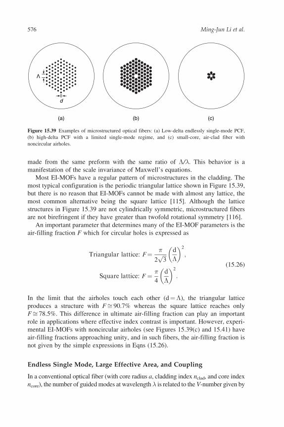
made from the same preform with the same ratio of �/�. This behavior is a
manifestation of the scale invariance of Maxwell’s equations.
Most EI-MOFs have a regular pattern of microstructures in the cladding. The
most typical configuration is the periodic triangular lattice shown in Figure 15.39,
but there is no reason that EI-MOFs cannot be made with almost any lattice, the
most common alternative being the square lattice [115]. Although the lattice
structures in Figure 15.39 are not cylindrically symmetric, microstructured fibers
are not birefringent if they have greater than twofold rotational symmetry [116].
An important parameter that determines many of the EI-MOF parameters is the
air-filling fraction F which for circular holes is expressed as
Triangular lattice: F=�
2ffiffiffi3p d
�
� �2
;
Square lattice: F =�
4
d
�
� �2
:
(15.26)
In the limit that the airholes touch each other (d = �), the triangular lattice
produces a structure with Fffi 90.7% whereas the square lattice reaches only
Fffi 78.5%. This difference in ultimate air-filling fraction can play an important
role in applications where effective index contrast is important. However, experi-
mental EI-MOFs with noncircular airholes (see Figures 15.39(c) and 15.41) have
air-filling fractions approaching unity, and in such fibers, the air-filling fraction is
not given by the simple expressions in Eqns (15.26).
Endless Single Mode, Large Effective Area, and Coupling
In a conventional optical fiber (with core radius a, cladding index nclad, and core index
ncore), the number of guided modes at wavelength� is related to the V-number given by
(a)
d
V
(b) (c)
Figure 15.39 Examples of microstructured optical fibers: (a) Low-delta endlessly single-mode PCF,
(b) high-delta PCF with a limited single-mode regime, and (c) small-core, air-clad fiber with
noncircular airholes.
576 Ming-Jun Li et al.
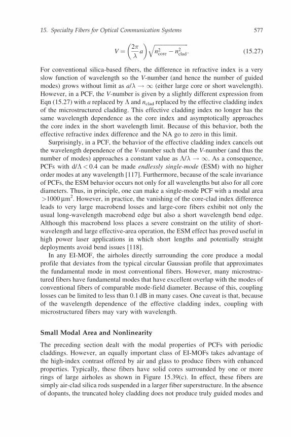
V =2�
�a
� � ffiffiffiffiffiffiffiffiffiffiffiffiffiffiffiffiffiffiffiffiffiffiffiffin2core � n2
clad
q: (15.27)
For conventional silica-based fibers, the difference in refractive index is a very
slow function of wavelength so the V-number (and hence the number of guided
modes) grows without limit as a/� ! 1 (either large core or short wavelength).
However, in a PCF, the V-number is given by a slightly different expression from
Eqn (15.27) with a replaced by � and nclad replaced by the effective cladding index
of the microstructured cladding. This effective cladding index no longer has the
same wavelength dependence as the core index and asymptotically approaches
the core index in the short wavelength limit. Because of this behavior, both the
effective refractive index difference and the NA go to zero in this limit.
Surprisingly, in a PCF, the behavior of the effective cladding index cancels out
the wavelength dependence of the V-number such that the V-number (and thus the
number of modes) approaches a constant value as �/� ! 1. As a consequence,
PCFs with d/�< 0.4 can be made endlessly single-mode (ESM) with no higher
order modes at any wavelength [117]. Furthermore, because of the scale invariance
of PCFs, the ESM behavior occurs not only for all wavelengths but also for all core
diameters. Thus, in principle, one can make a single-mode PCF with a modal area
>1000 mm2. However, in practice, the vanishing of the core-clad index difference
leads to very large macrobend losses and large-core fibers exhibit not only the
usual long-wavelength macrobend edge but also a short wavelength bend edge.
Although this macrobend loss places a severe constraint on the utility of short-
wavelength and large effective-area operation, the ESM effect has proved useful in
high power laser applications in which short lengths and potentially straight
deployments avoid bend issues [118].
In any EI-MOF, the airholes directly surrounding the core produce a modal
profile that deviates from the typical circular Gaussian profile that approximates
the fundamental mode in most conventional fibers. However, many microstruc-
tured fibers have fundamental modes that have excellent overlap with the modes of
conventional fibers of comparable mode-field diameter. Because of this, coupling
losses can be limited to less than 0.1 dB in many cases. One caveat is that, because
of the wavelength dependence of the effective cladding index, coupling with
microstructured fibers may vary with wavelength.
Small Modal Area and Nonlinearity
The preceding section dealt with the modal properties of PCFs with periodic
claddings. However, an equally important class of EI-MOFs takes advantage of
the high-index contrast offered by air and glass to produce fibers with enhanced
properties. Typically, these fibers have solid cores surrounded by one or more
rings of large airholes as shown in Figure 15.39(c). In effect, these fibers are
simply air-clad silica rods suspended in a larger fiber superstructure. In the absence
of dopants, the truncated holey cladding does not produce truly guided modes and
15. Specialty Fibers for Optical Communication Systems 577
can lead to high attenuation. However, in applications where low loss is more
critical, additional rows of holes can be added to produce similar optical perfor-
mance with improved attenuation.
The large index contrast in air-clad fibers requires a small core diameter to
achieve single-mode operation. This combination of high-index contrast and small
modal area can lead to high birefringence (in asymmetric designs), high disper-
sion, and high nonlinearity. In many applications, these properties are not desirable
and small modal area can make efficient coupling difficult. However, in nonlinear
device applications, the small modal area leads to significant nonlinear enhance-
ment and the dopant-free design lends itself to other nonsilica glass systems with
higher nonlinear coefficients. The resulting fibers [119] lead to enhanced nonlinear
interactions in short device lengths with low latency. However, because nonsilica
fibers have very high losses (>1 dB/m), nonlinear figures of merit that include
attenuation may remain lower than those obtained using silica fibers.
Dispersion
Dispersion is an important property in many optical fiber applications, and
although standard fiber designs offer a wide range of dispersion characteristics,
EI-MOFs broaden and extend this range to limits which may be difficult to achieve
with standard fiber-processing techniques [120]. The benefit comes from the large
index contrast of the airholes and because of the wavelength dependence of the
effective-cladding index described above.
Early work [121] concentrated on using air-clad EI-MOF designs that had large
air-filling fractions and small pitches to produce a very large waveguide dispersion
feature (see Figure 15.40). At long wavelengths, this feature produces a dispersion
Wavelength (nm)
D (
ps/n
m/k
m)
500
300
0
–300
–600
–900
–12001000 1500
Λ = 1000 nm
bulk materiald/Λ = 0.900.800.600.40
2000 2500
Figure 15.40 Modeled dispersion parameter for a standard air-silica PCF design with � = 1000 nm and
for a range of air-filling fractions. The material refractive index is also plotted.
578 Ming-Jun Li et al.
parameter D with a large negative component (less than–2000 ps/nm/km) that has
potential application in dispersion compensation for telecommunication. However,
such applications have been hampered by the nonlinearity and coupling issues
resulting from the small core size. At short wavelengths, the dispersive feature
produces a surprisingly large positive-D component (>100 ps/nm/km) that can be
used to balance the large material dispersion at visible wavelengths leading to
fibers with zero-dispersion wavelengths as low as 550 nm [122]. This zero-
dispersion wavelength combined with the small core size enables efficient non-
linear processes that lead to dramatic effects such as broadband continuum
generation [123].
More recently, EI-MOF designs have focused on slope compensation [120] and
dispersion-flattened [124] designs. These designs, with more complex core geo-
metries, have more reasonable effective areas (>40 mm2), but the performance
improvement over conventional fiber has not been sufficient to drive commercial
application.
Attenuation
Although early EI-MOF fibers had losses >100 dB/km, improvements in proces-
sing and design now yield silica-based EI-MOFs with attenuation as low as
0.28 dB/km [125]. It has been suggested that EI-MOFs might be the ultimate
low-loss fiber because of the absence of all dopants. However, the large index
contrast greatly enhances scattering at the air/silica interfaces and can lead to
excess scattering losses, which are typically negligible in conventional fibers.
The attenuation can be very dependant on the air-filling fraction, the pitch �,
and the water content in the fiber [126], thus it is not possible to achieve low
attenuation in every application, especially those in which the light is confined to a
very small core diameter. However, in most applications, transmission losses can
be expected to be on the order of 0.5–5 dB/km.
As mentioned in the discussion of ESM, macrobending losses can be very
significant in EI-MOFs at long and short wavelengths. However, if designed
correctly, holey fibers can achieve excellent bend loss especially when used in
combination with more conventional fiber designs [127]. Such designs have been
suggested for FTTH applications but have yet to achieve acceptance because of
their nonstandard modal properties and higher production cost.
Microbending in EI-MOFs has received little attention, but it is predicted to be
somewhat better than conventional fibers [128].
15.6.4 Hollow-Core PBGF
The second major class of microstructured optical fibers is the PBGF. The first
demonstration of guiding light in air with a 2D dielectric PBGF was reported in
1999 [112]. While those initial demonstrations were in fibers only a few
15. Specialty Fibers for Optical Communication Systems 579
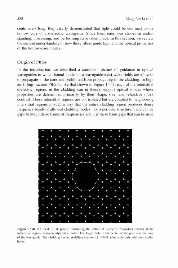
centimeters long, they clearly demonstrated that light could be confined to the
hollow core of a dielectric waveguide. Since then, enormous strides in under-
standing, processing, and performing have taken place. In this section, we review
the current understanding of how these fibers guide light and the optical properties
of the hollow-core modes.
Origin of PBGs
In the introduction, we described a consistent picture of guidance in optical
waveguides in which bound modes of a waveguide exist when fields are allowed
to propagate in the core and prohibited from propagating in the cladding. In high
air-filling fraction PBGFs, like that shown in Figure 15.41, each of the interstitial
dielectric regions in the cladding can in theory support optical modes whose
properties are determined primarily by their shape, size, and refractive index
contrast. These interstitial regions are not isolated but are coupled to neighboring
interstitial regions in such a way that the entire cladding region produces dense
frequency bands of allowed cladding modes. For a periodic structure, there can be
gaps between these bands of frequencies and it is these band gaps that can be used
Figure 15.41 An ideal PBGF profile illustrating the lattice of dielectric resonators formed at the
interstitial regions between adjacent airholes. The larger hole in the center of the profile is the core
of the waveguide. The cladding has an air-filling fraction of >94% achievable only with noncircular
holes.
580 Ming-Jun Li et al.
to confine light to defects in the periodic structure. The defect serves as a core of
the waveguide.
Most PBGFs have employed a triangular lattice, which is mechanically
robust and resistant to perturbation. The practical benefit of other lattices has
not been demonstrated for hollow-core fibers and many lattices, in fact, produce
smaller more fragmented band gaps unsuitable for hollow-core guidance. The
exception is a so-called Kagome lattice that has no band gaps to support
hollow-core guidance but has found applications nonetheless in enhancing the
interaction between optical fields and atoms and molecules filling the hollow
core [129]. As in the case of EI-MOF, air fraction plays the key role in
determining the band-gap width, as well as the dispersion, loss, and nonlinearity
of the core modes. In addition, it also affects the position of the band gap. In
air-silica PBGF, larger air fraction increases the band-gap width and decreases
the center wavelength of the band gap.
The finite frequency range of these band gaps limits the bandwidth of operation
for band-gap-guided modes. However, normalized band-gap widths, D!/! (the
spectral width of the gap divided by the central frequency of the gap), as large as
0.3 have been demonstrated [130], which translates to a 500-nm bandwidth
centered at 1500 nm. As mentioned previously, if material dispersion can be
neglected, Maxwell’s equations are scale invariant. Therefore, the center fre-
quency of the band gap can be shifted to longer or shorter wavelengths by
respectively increasing or decreasing the scale of the PBGF profile. If the geome-
try of the fiber profile is maintained through these scale changes, then the normal-
ized band-gap width remains unchanged.
The core of a PBGF is defined by a defect formed in the photonic crystal lattice,
typically through the removal of a series of adjacent capillaries. The removal of
seven adjacent capillaries forms a hexagonal defect in the profile. This core has
been demonstrated to support three to five different transverse mode profiles
[130, 131]. Larger defects have also been demonstrated; removing the next row
of capillaries results in a 19-cell core [131]. Similar to conventional optical fibers,
large-core PBGFs support additional higher-order modes.
Dispersion in Hollow-Core PBGF
Two important attributes of fiber propagation are chromatic and modal dispersion.
In this section we discuss chromatic and modal dispersion, as well as the transverse
profiles of the bound modes associated with hollow-core PBGFs.
If we think of PBGFs as waveguides that prohibit propagating modes in the
cladding, a simple analytical model can be used to approximate the boundary
between the core and cladding, treating the PBGF as a perfectly reflecting hollow
cylinder [113]. This approach is a very good approximation for estimating the
dispersion and mode profiles in hollow-core PBGFs. More accurate descriptions of
these and other optical properties require numerical modeling, which can be
accomplished using a variety of techniques [132–135]. The modes and dispersion
15. Specialty Fibers for Optical Communication Systems 581
of a perfectly reflecting hollow cylinder have the simple relationship between the
frequency, !, and propagation constant, �, of the modes:
n2!2
c2= �2 þ jpq
R
� �2
; (15.28)
where n is the refractive index of the core material, R is the radius of the core, c
is the speed of light in a vacuum, and jpq is the qth zero of the pth-order Bessel
function of the first kind. It is convenient to recast Eqn (15.28) in terms of the
effective index of the mode, neff � �c/!:
n2eff = n2 � jpqc
!R
� �2
: (15.29)
Interestingly, the effective indices of these modes are less than the index of the
core material, n. For a hollow core, with n = 1, the mode effective index is less
than one, which means the phase fronts propagate in the fiber with a velocity
greater than the speed of light in vacuum. The group velocity of such modes is less
than the speed of light in vacuum and the effective group index, ng, is given by
ng = neff þ !dneff
d!= 1=neff: (15.30)
The fundamental mode of the hollow core is characterized by the first zero of
the zeroth-order Bessel function, j01 ffi 2.4048. In Figure 15.42, we plot the band
gaps associated with the PBGF profile shown in Figure 15.41, along with the
dispersion of the hollow-core modes of Eqn (15.29). The calculated core modes of
the profile are in close agreement with the modes of a perfectly reflecting hollow
cylinder, except for the regions near the band edges, where coupling between the
core and band modes causes the dispersion of the core mode to deviate from that of
a perfectly reflecting hollow cylinder mode.
Unlike conventional optical fibers, some PBGF designs also support modes that
exist on the boundary between the core and the periodic lattice [44, 136]. Due to
their strong localization to small glass regions of the fiber profile, these surface
modes are highly susceptible to structural variations in these regions. This results
in significantly higher losses for these modes as compared with hollow-core
modes, which have a much smaller overlap with the glass structure and thus
experience a smaller impact due to structural variations. The surface modes have
very different dispersion from the core modes (see Figure 15.42), which results in a
strong interaction between the modes that have the same propagation constant at
a given frequency. When the symmetry of a surface mode is the same as that of a
core mode, they can interact strongly and result in an anticrossing, as seen in
Figure 15.42. This strong interaction and mixing of the modes lead to increased
attenuation of core-guided modes at frequencies near these crossing regions.
582 Ming-Jun Li et al.
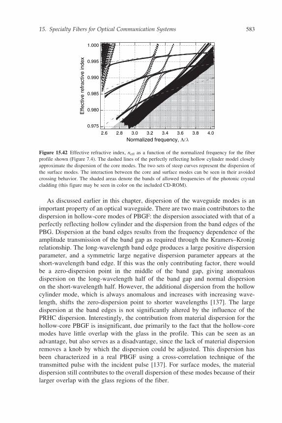
As discussed earlier in this chapter, dispersion of the waveguide modes is an
important property of an optical waveguide. There are two main contributors to the
dispersion in hollow-core modes of PBGF: the dispersion associated with that of a
perfectly reflecting hollow cylinder and the dispersion from the band edges of the
PBG. Dispersion at the band edges results from the frequency dependence of the
amplitude transmission of the band gap as required through the Kramers–Kronig
relationship. The long-wavelength band edge produces a large positive dispersion
parameter, and a symmetric large negative dispersion parameter appears at the
short-wavelength band edge. If this was the only contributing factor, there would
be a zero-dispersion point in the middle of the band gap, giving anomalous
dispersion on the long-wavelength half of the band gap and normal dispersion
on the short-wavelength half. However, the additional dispersion from the hollow
cylinder mode, which is always anomalous and increases with increasing wave-
length, shifts the zero-dispersion point to shorter wavelengths [137]. The large
dispersion at the band edges is not significantly altered by the influence of the
PRHC dispersion. Interestingly, the contribution from material dispersion for the
hollow-core PBGF is insignificant, due primarily to the fact that the hollow-core
modes have little overlap with the glass in the profile. This can be seen as an
advantage, but also serves as a disadvantage, since the lack of material dispersion
removes a knob by which the dispersion could be adjusted. This dispersion has
been characterized in a real PBGF using a cross-correlation technique of the
transmitted pulse with the incident pulse [137]. For surface modes, the material
dispersion still contributes to the overall dispersion of these modes because of their
larger overlap with the glass regions of the fiber.
Effe
ctiv
e re
frac
tive
inde
x
1.000
0.995
0.990
0.985
0.980
0.975
4.03.83.63.43.23.02.82.6
Normalized frequency, Λ/λ
Figure 15.42 Effective refractive index, neff as a function of the normalized frequency for the fiber
profile shown (Figure 7.4). The dashed lines of the perfectly reflecting hollow cylinder model closely
approximate the dispersion of the core modes. The two sets of steep curves represent the dispersion of
the surface modes. The interaction between the core and surface modes can be seen in their avoided
crossing behavior. The shaded areas denote the bands of allowed frequencies of the photonic crystal
cladding (this figure may be seen in color on the included CD-ROM).
15. Specialty Fibers for Optical Communication Systems 583
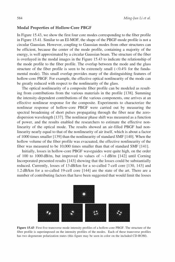
Modal Properties of Hollow-Core PBGF
In Figure 15.43, we show the first four core modes corresponding to the fiber profile
in Figure 15.41. Similar to an EI-MOF, the shape of the PBGF-mode profile is not a
circular Gaussian. However, coupling to Gaussian modes from other structures can
be efficient, because the center of the mode profile, containing a majority of the
energy, is well approximated by a circular Gaussian beam. The structure of the fiber
is overlayed in the modal images in the Figure 15.43 to indicate the relationship of
the mode profile to the fiber profile. The overlap between the mode and the glass
structure of the fiber profile is seen to be extremely small (<0.4% for the funda-
mental mode). This small overlap provides many of the distinguishing features of
hollow-core PBGF. For example, the effective optical nonlinearity of the mode can
be greatly reduced with respect to the nonlinearity of the glass.
The optical nonlinearity of a composite fiber profile can be modeled as result-
ing from contributions from the various materials in the profile [138]. Summing
the intensity-dependent contributions of the various components, one arrives at an
effective nonlinear response for the composite. Experiments to characterize the
nonlinear response of hollow-core PBGF were carried out by measuring the
spectral broadening of short pulses propagating through the fiber near the zero-
dispersion wavelength [137]. The nonlinear phase shift was measured as a function
of power, and the results enabled the researchers to estimate the effective non-
linearity of the optical mode. The results showed an air-filled PBGF had non-
linearity nearly equal to that of the nonlinearity of air itself, which is about a factor
of 1000 times smaller [139] than the nonlinearity of standard SMF [140]. When the
hollow volume of the fiber profile was evacuated, the effective nonlinearity of the
fiber was measured to be 10,000 times smaller than that of standard SMF [141].
Initially, losses in hollow-core PBGF waveguides were quite high, on the order
of 100 to 1000 dB/m, but improved to values of 1 dB/m [142] until Corning
Incorporated presented results [143] showing that the losses could be substantially
reduced. Currently, losses of 13 dB/km for a so-called 7-cell core [130, 143] and
1.2 dB/km for a so-called 19-cell core [144] are the state of the art. There are a
number of contributing factors that have been suggested that would limit the losses
Figure 15.43 First five transverse mode intensity profiles of a hollow-core PBGF. The structure of the
fiber profile is superimposed on the intensity profiles of the modes. Each of these transverse profiles
has two degenerate polarization states (this figure may be seen in color on the included CD-ROM).
584 Ming-Jun Li et al.
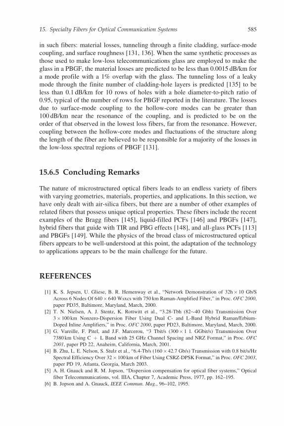
in such fibers: material losses, tunneling through a finite cladding, surface-mode
coupling, and surface roughness [131, 136]. When the same synthetic processes as
those used to make low-loss telecommunications glass are employed to make the
glass in a PBGF, the material losses are predicted to be less than 0.0015 dB/km for
a mode profile with a 1% overlap with the glass. The tunneling loss of a leaky
mode through the finite number of cladding-hole layers is predicted [135] to be
less than 0.1 dB/km for 10 rows of holes with a hole diameter-to-pitch ratio of
0.95, typical of the number of rows for PBGF reported in the literature. The losses
due to surface-mode coupling to the hollow-core modes can be greater than
100 dB/km near the resonance of the coupling, and is predicted to be on the
order of that observed in the lowest loss fibers, far from the resonance. However,
coupling between the hollow-core modes and fluctuations of the structure along
the length of the fiber are believed to be responsible for a majority of the losses in
the low-loss spectral regions of PBGF [131].
15.6.5 Concluding Remarks
The nature of microstructured optical fibers leads to an endless variety of fibers
with varying geometries, materials, properties, and applications. In this section, we
have only dealt with air-silica fibers, but there are a number of other examples of
related fibers that possess unique optical properties. These fibers include the recent
examples of the Bragg fibers [145], liquid-filled PCFs [146] and PBGFs [147],
hybrid fibers that guide with TIR and PBG effects [148], and all-glass PCFs [113]
and PBGFs [149]. While the physics of the broad class of microstructured optical
fibers appears to be well-understood at this point, the adaptation of the technology
to applications appears to be the main challenge for the future.
REFERENCES
[1] K. S. Jepsen, U. Gliese, B. R. Hemenway et al., “Network Demonstration of 32h� 10 Gb/S
Across 6 Nodes Of 640� 640 Wsxcs with 750 km Raman-Amplified Fiber,” in Proc. OFC 2000,
paper PD35, Baltimore, Maryland, March, 2000.
[2] T. N. Nielsen, A. J. Stentz, K. Rottwitt et al., “3.28-Tbh (8240 Gbh) Transmission Over
3� 100 km Nonzero-Dispersion Fiber Using Dual C- and L-Band Hybrid Raman/Erbium-
Doped Inline Amplifiers,” in Proc. OFC 2000, paper PD23, Baltimore, Maryland, March, 2000.
[3] G. Vareille, F. Pitel, and J.F. Marcerou, “3 Tbit/s (300� 1 l. GGbit/s) Transmission Over
7380 km Using C þ L Band with 25 GHz Channel Spacing and NRZ Format,” in Proc. OFC
2001, paper PD 22, Anaheim, California, March, 2001.
[4] B. Zhu, L. E. Nelson, S. Stulz et al., “6.4-Tb/s (160� 42.7 Gb/s) Transmission with 0.8 bit/s/Hz
Spectral Efficiency Over 32� 100 km of Fiber Using CSRZ-DPSK Format,” in Proc. OFC 2003,
paper PD 19, Atlanta, Georgia, March 2003.
[5] A. H. Gnauck and R. M. Jopson, “Dispersion compensation for optical fiber systems,” Optical
fiber Telecommunications, vol. IIIA, Chapter 7, Academic Press, 1977, pp. 162–195.
[6] B. Jopson and A. Gnauck, IEEE Commun. Mag., 96–102, 1995.
15. Specialty Fibers for Optical Communication Systems 585
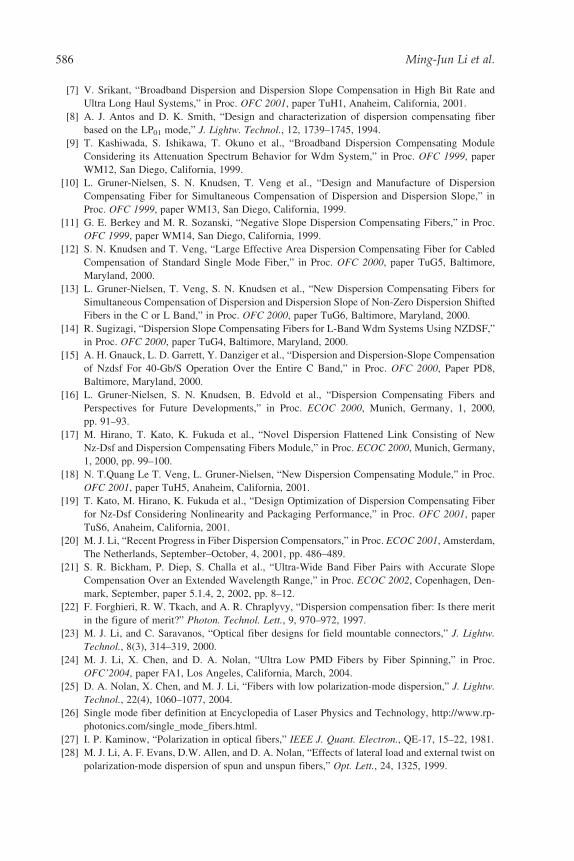
[7] V. Srikant, “Broadband Dispersion and Dispersion Slope Compensation in High Bit Rate and
Ultra Long Haul Systems,” in Proc. OFC 2001, paper TuH1, Anaheim, California, 2001.
[8] A. J. Antos and D. K. Smith, “Design and characterization of dispersion compensating fiber
based on the LP01 mode,” J. Lightw. Technol., 12, 1739–1745, 1994.
[9] T. Kashiwada, S. Ishikawa, T. Okuno et al., “Broadband Dispersion Compensating Module
Considering its Attenuation Spectrum Behavior for Wdm System,” in Proc. OFC 1999, paper
WM12, San Diego, California, 1999.
[10] L. Gruner-Nielsen, S. N. Knudsen, T. Veng et al., “Design and Manufacture of Dispersion
Compensating Fiber for Simultaneous Compensation of Dispersion and Dispersion Slope,” in
Proc. OFC 1999, paper WM13, San Diego, California, 1999.
[11] G. E. Berkey and M. R. Sozanski, “Negative Slope Dispersion Compensating Fibers,” in Proc.
OFC 1999, paper WM14, San Diego, California, 1999.
[12] S. N. Knudsen and T. Veng, “Large Effective Area Dispersion Compensating Fiber for Cabled
Compensation of Standard Single Mode Fiber,” in Proc. OFC 2000, paper TuG5, Baltimore,
Maryland, 2000.
[13] L. Gruner-Nielsen, T. Veng, S. N. Knudsen et al., “New Dispersion Compensating Fibers for
Simultaneous Compensation of Dispersion and Dispersion Slope of Non-Zero Dispersion Shifted
Fibers in the C or L Band,” in Proc. OFC 2000, paper TuG6, Baltimore, Maryland, 2000.
[14] R. Sugizagi, “Dispersion Slope Compensating Fibers for L-Band Wdm Systems Using NZDSF,”
in Proc. OFC 2000, paper TuG4, Baltimore, Maryland, 2000.
[15] A. H. Gnauck, L. D. Garrett, Y. Danziger et al., “Dispersion and Dispersion-Slope Compensation
of Nzdsf For 40-Gb/S Operation Over the Entire C Band,” in Proc. OFC 2000, Paper PD8,
Baltimore, Maryland, 2000.
[16] L. Gruner-Nielsen, S. N. Knudsen, B. Edvold et al., “Dispersion Compensating Fibers and
Perspectives for Future Developments,” in Proc. ECOC 2000, Munich, Germany, 1, 2000,
pp. 91–93.
[17] M. Hirano, T. Kato, K. Fukuda et al., “Novel Dispersion Flattened Link Consisting of New
Nz-Dsf and Dispersion Compensating Fibers Module,” in Proc. ECOC 2000, Munich, Germany,
1, 2000, pp. 99–100.
[18] N. T.Quang Le T. Veng, L. Gruner-Nielsen, “New Dispersion Compensating Module,” in Proc.
OFC 2001, paper TuH5, Anaheim, California, 2001.
[19] T. Kato, M. Hirano, K. Fukuda et al., “Design Optimization of Dispersion Compensating Fiber
for Nz-Dsf Considering Nonlinearity and Packaging Performance,” in Proc. OFC 2001, paper
TuS6, Anaheim, California, 2001.
[20] M. J. Li, “Recent Progress in Fiber Dispersion Compensators,” in Proc. ECOC 2001, Amsterdam,
The Netherlands, September–October, 4, 2001, pp. 486–489.
[21] S. R. Bickham, P. Diep, S. Challa et al., “Ultra-Wide Band Fiber Pairs with Accurate Slope
Compensation Over an Extended Wavelength Range,” in Proc. ECOC 2002, Copenhagen, Den-
mark, September, paper 5.1.4, 2, 2002, pp. 8–12.
[22] F. Forghieri, R. W. Tkach, and A. R. Chraplyvy, “Dispersion compensation fiber: Is there merit
in the figure of merit?” Photon. Technol. Lett., 9, 970–972, 1997.
[23] M. J. Li, and C. Saravanos, “Optical fiber designs for field mountable connectors,” J. Lightw.
Technol., 8(3), 314–319, 2000.
[24] M. J. Li, X. Chen, and D. A. Nolan, “Ultra Low PMD Fibers by Fiber Spinning,” in Proc.
OFC’2004, paper FA1, Los Angeles, California, March, 2004.
[25] D. A. Nolan, X. Chen, and M. J. Li, “Fibers with low polarization-mode dispersion,” J. Lightw.
Technol., 22(4), 1060–1077, 2004.
[26] Single mode fiber definition at Encyclopedia of Laser Physics and Technology, http://www.rp-
photonics.com/single_mode_fibers.html.
[27] I. P. Kaminow, “Polarization in optical fibers,” IEEE J. Quant. Electron., QE-17, 15–22, 1981.
[28] M. J. Li, A. F. Evans, D.W. Allen, and D. A. Nolan, “Effects of lateral load and external twist on
polarization-mode dispersion of spun and unspun fibers,” Opt. Lett., 24, 1325, 1999.
586 Ming-Jun Li et al.
[29] X. Chen, M.-J. Li, and D. A. Nolan, “Polarization Evolution in Spun Fibers,” in Proc. SPIE,
Shanghai, China, 6019, 2005, pp. 60192J.
[30] J. Noda, K. Okamoto, and Y. Sasaki, “Polarization-Maintaining Fibers and Their Applications,”
J. Lightw. Technol., LT-4, 1071–1089, 1986.
[31] T. Hosaka, K. Okamoto, T. Miya et al., “Low-loss single-polarization fibers with asymmetrical
strain birefringence,” Electron. Lett., 17, 530–531, 1981.
[32] M. P. Varnham, D. N. Payne, R. D. Birch, and E. J. Tarbox, “Single-polarization operation of
highly birefringent bow-tie optical fibers,” Electron. Lett., 19, 246–247, 1983.
[33] T. Katsuyama, H. Matsumura, and T. Suganuma, “Propagation characteristics of single polariza-
tion fibers,” Appl. Opt., 22, 1748–1753, 1983.
[34] R. B. Dyott, J. R. Cozens, and D. G. Morris, “Preservation of polarization in optical-fiber
waveguides with elliptical cores,” Electron. Lett., 15, 380–382, 1979.
[35] T. Okoshi, K. Oyamada, M. Nishimura, and H. Yokota, “Side-tunnel Fiber: An approach to
polarization-maintaining optical waveguiding scheme,” Electron. Lett., 18, 824–826, 1982.
[36] A. Ortigosa-Blanch, J. C. Knight, W. J. Wadsworth et al., “Highly birefringent photonic crystal
fibers,” Opt. Lett., 25, 1325–1327, 2000.
[37] T. P. Hansen, J. Broeng, S. E. B. Libori et al., “Highly birefrigent index-guiding photonic crystal
fibers,” IEEE Photon. Technol. Lett., 13, 588–590, 2001.
[38] K. Suzuki, H. Kubota, S. Kawanishi et al., “Optical properties of a low-loss polarization-
maintaining photonic crystal fiber,” Opt. Express, 9, 676–680, 2001.
[39] J. R. Folkenberg, M. D. Nielsen, N. A. Mortensen et al., “Polarization maintaining large mode
area photonic crystal fiber,” Opt. Express, 12, 956–960, 2004.
[40] K. Saitoh and M. Koshiba, “Photonic bandgap fibers with high birefringence,” IEEE Photon.
Technol. Lett., 14, 1291–1293, 2002.
[41] X. Chen, M.-J. Li, N. Venkataraman et al., “Highly birefringent hollow-core photonic bandgap
fiber,” Opt. Express, 12, 3888–3893, 2004.
[42] M. S. Alam, K. Saitoh, and M. Koshiba, “High group birefringence in air-core photonic bandgap
fibers,” Opt. Lett., 30, 824–826, 2005.
[43] K. Saitoh, N. A. Mortensen, and M. Koshiba, “Air-core photonic band-gap fibers: the impact of
surface modes,” Opt. Express, 12, 394, 2004.
[44] J. A. West, C. M. Smith, N. F. Borrelli et al., “Surface modes in air-core photonic band-gap
fibers,” Opt. Express., 12, 1485, 2004.
[45] K. Saitoh, N. Florous, T. Murao, and M. Koshiba, “Design of Large Hollow-Core Photonic Band-
Gap Fibers with Suppressed Higher-Order Modes,” in Proc. OFC/ENFOEC CD-ROM 2007,
paper OML2, Washington, DC, Optical Society of America, 2007.
[46] J. R. Simpson, R. H. Stolen, F. M. Sears et al., “A Single polarization fiber,” J. Lightw. Technol.,
LT-1, 370–373, 1983.
[47] M. J. Messerly, J. R. Onstott, and R. C. Mikkelson, “A broad-band single polarization optical
fiber,” J. Lightw. Technol., 9, 817, 1991.
[48] D. A. Nolan, G. E. Berkey, M.-J. Li et al., “Single-polarization fiber with a high extinction ratio,”
Opt. Lett., 29, 1855, 2004.
[49] D. A. Nolan, M.-J. Li, X. Chen, and J. Koh, “Single Polarization Fibers and Applications,” in
Proc. OFC/ENFOEC CD-ROM 2006, paper OWA1, Washington, DC, Optical Society of
America, 2006.
[50] M.-J. Li, X. Chen, J. Wang et al., “Fiber Designs for Higher Power Lasers,” in Proc. SPIE,
San Jose, California, 6469, 2007, pp. 64690H.
[51] H. Kubota, S. Kawanishi, S. Koyanagi et al., “Absolutely Single Polarization Photonic Crystal
Fiber,” IEEE Photon. Technol. Lett., 16, 182, 2004.
[52] J. R. Folkenberg, M. D. Nielsen, and C. Jakobsen, “Broadband single-polarization photonic
crystal fiber,” Opt. Lett., 30, 1446–1448, 2005.
[53] T. Schreiber, F. Roser, O. Schmidt et al., “Stress-induced single-polarization single-transverse
mode photonic crystal fiber with low nonlinearity,” Opt. Express, 13, 7621–7630, 2005.
15. Specialty Fibers for Optical Communication Systems 587
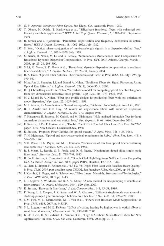
[54] G. P. Agrawal, Nonlinear Fiber Optics, San Diego, CA, Academic Press, 1989.
[55] T. Okuno, M. Onishi, T. Kashiwada et al., “Silica-base functional fibers with enhanced non-
linearity and their applications,” IEEE J. Sel. Top. Quant. Electron., 5, 1385–1391, September
1999.
[56] R. Stolen and J. Bjorkholm, “Parametric amplification and frequency conversion in optical
fibers,” IEEE J. Quant. Electron., 18, 1062–1072, July 1982.
[57] S. Wen, “Optical phase conjugation of multiwavelength signals in a dispersion-shifted fiber,”
J. Lightw. Technol., 15, 1061–1070, July 1997.
[58] M. Sauer, D. Nolan, M. Li, and G. Berkey, “Simultaneous Multichannel Pulse Compression for
Broadband Dynamic Dispersion Compensation,” in Proc. OFC 2003, Atlanta, Georgia, March, 1,
2003, pp. 23–28, 298–300.
[59] S. Li, M. Sauer, Z. D. Gaeta et al., “Broad-band dynamic dispersion compensation in nonlinear
fiber-based device,” J. Lightw. Technol., 22, 29–38, January 2004.
[60] H. A. Haus, “Optical Fiber Solitons, Their Properties and Uses,” in Proc. IEEE, 81, July 1993, pp.
970–983.
[61] Ming-Jun Li, Shenping Li, and Daniel A. Nolan, “Nonlinear Fibers for Signal Processing Using
Optical Kerr Effects,” J. Lightw. Technol., 23(11), 3606–3614, 2005.
[62] D. Q. Chowdhury and D. A. Nolan, “Perturbation model for computingoptical fiber birefringence
from two-dimensional refractive index profile,” Opt. Lett., 20, 1973–1975, 1995.
[63] M. J. Li and D. A. Nolan, “Fiber spin-profile designs for producing fibers with low polarization
mode dispersion,” Opt. Lett., 23, 1659–1661, 1998.
[64] M. J. Adams, An Introduction to Optical Waveguides, Chichester, John Wiley & Sons Ltd., 1981.
[65] B. J. Ainslie and C.R. Day, “A review of single-mode fibers with modified dispersion
characteristics,” J. Lightw. Technol., 4, 967–979, August 1986.
[66] T. Hasegawa, E. Sasaoka, M. Onishi, and M. Nishimura, “Hole-assisted lightguide fiber for large
anomalous dispersion and low optical loss,” Opt. Express., 9, 681–686, December 2001.
[67] E. Snitzer, H. Po, F. Hakimi et al., “Double Clad Offset Core Nd Fiber Laser,” in Proc. OFSTM,
paper PD 5, New Orleans, Louisiana/USA, 1988.
[68] E. Snitzer, “Proposed Fiber Cavities for optical masers,” J. Appl. Phys., 32(1), 36, 1961.
[69] T. H. Mainman, “Optical and microwave optical experiments in Ruby,” Phys. Rev. Lett., 4(11),
564–566, 1960.
[70] S. B. Poole, D. N. Payne, and M. E. Fermann, “Fabrication of low loss optical fibers containing
rare-earth ions,” Electron. Lett., 21, 737–738, 1985.
[71] R. J. Mears, L. Reekie, S. B. Poole, and D. N. Payne, “Neodymium-doped silica single-mode
fibre laser,” Electron. Lett., 21, 738–740, 1985.
[72] H. Po, E. Snitzer, R. Tumminelli et al., “Double Clad High Brightness Nd Fiber Laser Pumped by
GaAlAs Phased Array,” in Proc. OFC, paper PDP7, Houston, TX/USA, 1989.
[73] A. Liem, J. Limpert, H. Zellmer et al., “1.3 kW Yb-Doped Fiber Laser with Excellent Beam Quality,”
in Proc. CLEO 2004, post-deadline paper CPDD2, San Francisco, USA, May, 2004, pp. 16–21.
[74] J. Kirchhof, S. Unger, and A. Schwuchow, “Fiber Lasers: Materials, Structures and Technologies,”
in Proc. SPIE, 4957, 2003, pp. 1–15.
[75] J. P. Koplow, S. W. Moore, and D. A. V. Kliner, “A new method for side pumping of double-clad
fiber sources,” J. Quant. Elelectron., 39(4), 529–540, 2003.
[76] E. Snitzer, “Rare-earth fiber laser,” J. LessCommon Met., 148, 45–58, 1989.
[77] P. Wang, L. J. Cooper, J. K. Sahu, and W. A. Clarkson, “Efficient single-mode operation of a
cladding-pumped ytterbium-doped helical-core fiber laser,” Opt. Lett., 31, 226–228, 2006.
[78] J. M. Fini, M. D. Mermelstein, M. F. Yan et al., “Fibers with Resonant Mode Suppression,” in
Proc. SPIE, 6453, 2007, p. 64530F.
[79] S. L. Logunov and M. E. DeRosa, “Effect of coating heating by high power in optical fibres at
small bend diameters,” Electron. Lett., 39, 897–898, 2003.
[80] K. -F. Klein, H. S. Eckhardt, C. Vincze et al., “High NA-Fibers: Silica-Based Fibers for New
Applications,” in Proc. SPIE, San Jose, California, 5691, 2005, pp. 30–41.
588 Ming-Jun Li et al.
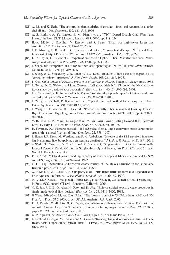
[81] A. Liu and K. Ueda, “The absorption characteristics of circular, offset, and rectangular double-
clad fibers,” Opt. Commun., 132, 511–518, 1996.
[82] A. S. Kurkov, A. Yu. Laptev, E. M. Dianov et al., “Yb3þ -Doped Double-Clad Fibers and
Lasers,” in Proc. SPIE, Moscow, Russia, 4083, 2000, pp. 118–126.
[83] H.–R. Muller, J. Kirchhof, V. Reichel, and S. Unger “Fibers for high-power lasers and
amplifiers,” C. R. Physique, 7, 154–162, 2006.
[84] J. D. Minelly, E. R. Taylor, K. P. Jedrzejewski et al., “Laser-Diode-Pumped Nd-Doped Fiber
Laser with Output Power > 1W,” in Proc. CLEO 1992, Anaheim, CA, 1995, p. 246.
[85] E. R. Taylor, D. Taylor et al. “Application-Specific Optical Fibers Manufactured from Multi-
component Glasses,” in Proc. MRS, 172, 1990, pp. 321–327.
[86] J. Schneider, “Properties of a fluoride fiber laser operating at 3.9 mm,” in Proc. SPIE, Denver,
Colorado, 2841, 1996, pp. 230–236.
[87] J. Wang, W. S. Brocklesby, J. R. Lincoln et al., “Local structures of rare-earth ions in glasses: the
‘crystal-chemistry’ approach,” J. Non-Cryst. Solids, 163, 261–267, 1993.
[88] F. Gan, Calculations of Physical Properties of Inorganic Glasses, Shanghai science press, 1978.
[89] J. Wang, D. T. Walton, and L.A. Zenteno, “All-glass, high NA, Yb-doped double-clad laser
fibers made by outside-vapor deposition”, Electron. Lett., 40(10), 590–592, 2004.
[90] J. E. Townsend, S. B. Poole, and D. N. Payne, “Solution-doping technique for fabrication of rare-
earth-doped optical fibers,” Electron. Lett., 23, 329–331, 1987.
[91] J. Wang, R. Kimball, R. Knowlton et al., “Optical fiber and method for making such fiber,”
Patent Application WO2005082801A2, 2005.
[92] J. Wang, D. T. Walton, M. J. Li et al., “Recent Specialty Fiber Research at Corning Towards
High-Power and High-Brightness Fiber Lasers”, in Proc. SPIE, 6028, 2005, pp. 6028021–
6028026.
[93] V. Reichel, K. W. Moerl, S. Unger et al., “Fiber-Laser Power Scaling Beyond the 1-Kilowatt
Level by Nd:Yb Co-Doping,” in Proc. SPIE, 5777, 2005, pp. 404–407.
[94] D. Taverner, D. J. Richardson et al., “158-mJ pulses from a single-transverse-mode, large-mode-
area erbium-doped fiber amplifier,” Opt. Lett., 22, 378, 1997.
[95] J. Hansryd, F. Dross, M. Westlund, and P. A. Andrekson, “Increase of the SBS threshold in a short
highly nonlinear fiber by applying a temperature distribution,” J. Lightw. Technol., 19(11), 1691, 2001.
[96] A.Wada, T. Nozawa, D. Tanaka, and R. Yamauchi, “Suppression of SBS by Intentionally
Induced Periodic Residual-Strain in Single-Mode Optical Fibers,” in Proc. 17th ECOC, paper
No.B1.1, Paris, France, 1991.
[97] R. G. Smith, “Optical power handling capacity of low-loss optical fiber as determined by SRS
and SBS,” Appl. Opt., 11, 2489–2494, 1972.
[98] C. L. Tang, “Saturation and spectral characteristics of the stokes emission in the stimulated
Brillouin process,” J. Appl. Phys., 37, 2945, 1966.
[99] X. P. Mao, R. W. Tkach, A. R. Chraplyvy et al., “Stimulated Brillouin threshold dependence on
fiber type and uniformity,” IEEE Photon. Technol. Lett., 4, 66–69, 1992.
[100] M. -J. Li, X. Chen, J. Wang et al., “Fiber Designs for Reducing Stimulated Brillouin Scattering,”
in Proc. OFC, paper# OTuA4, Anaheim, California, 2006.
[101] C. K. Jen, J. E. B. Oliveira, N. Goto, and K. Abe, “Role of guided acoustic wave properties in
single-mode optical fiber design,” Electron. Lett., 24, 1419–1420, 1988.
[102] Ji Wang, Ming-Jun, Li, and Dan Nolan, “The Lowest Loss of 0.35 dB/km in an Al-Doped SM
Fiber”, in Proc. OFC 2006, paper OThA1, Anaheim, CA, USA, 2006.
[103] P. D. Draglc, C. -H. Liu, G. C. Papen, and Almantas Galvanauskas, “Optical Fiber with an
Acoustic Guiding Layer for Stimulated Brillouin Scattering Suppression,” in Proc. CLEO 2005,
paper CThZ3, San Jose, California, 2005.
[104] G. P. Agrawal, Nonlinear Fiber Optics, San Diego, CA, Academic Press, 1989.
[105] J. Kirchhof, S. Unger, V. Reichel, and St. Grimm, “Drawing-Dependent Losses in Rare-Earth and
Heavy Metal Doped Silica Optical Fibers,” in Proc. OFC 1997, paper WL21, 1997, Dallas, TX/
USA, 1997.
15. Specialty Fibers for Optical Communication Systems 589
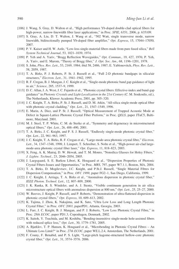
[106] J. Wang, S. Gray, D. Walton et al., “High performance Yb-doped double-clad optical fibers for
high-power, narrow-linewidth fiber laser applications,” in Proc. SPIE, 6351, 2006, p. 635109.
[107] S. Gray, A. Liu, D. T. Walton, J. Wang et al., “502 Watt, single transverse mode, narrow
linewidth, bidirectionally pumped Yb-doped fiber amplifier,” Opt. Express, 15, 17044–17050,
2007.
[108] P. V. Kaiser and H. W. Astle, “Low-loss single-material fibers made from pure fused silica,” Bell
System Technical Journal, 53, 1021–1039, 1974.
[109] P. Yeh and A. Yariv, “Bragg Reflection Waveguides,” Opt. Commun., 19, 427, 1976; P. Yeh,
A. Yariv, and E. Marom, “Theory of Bragg fiber,” J. Opt. Soc. Am., 68, 1196–1201, 1978.
[110] S. John, Phys. Rev. Lett., 53, 2169, 1984; ibid 58, 2486, 1987; E. Yablonovitch, Phys. Rev. Lett.,
58, 2059, 1987.
[111] T. A. Birks, P. J. Roberts, P. St. J. Russell et al., “Full 2-D photonic bandgaps in silica/air
structures,” Electron. Lett., 31, 1941–1942, 1995.
[112] R. F. Cregan, B. J. Mangan, J. C. Knight et al., “Single-mode photonic band gap guidance of light
in air,” Science, 285, 1537–9, 1999.
[113] D. C. Allan, J. A. West, J. C. Fajardo et al., “Photonic crystal fibers: Effective-index and band-gap
guidance” in Photonic Crystals and Light Localization in the 21st Century (C. M. Soukoulis, ed.),
The Netherlands, Kluwer Academic Press, 2001, pp. 305–320.
[114] J. C. Knight, T. A. Birks, P. St. J. Russell, and D. M. Atkin, “All-silica single-mode optical fiber
with photonic crystal cladding,” Opt. Lett., 21, 1547–1549, 1996.
[115] E. Marin, A. Diez, and P. St. J. Russell, “Optical Measurement of Trapped Acoustic Mode at
Defect in Square-Lattice Photonic Crystal Fiber Preform,” in Proc. QELS, paper JTuC5, Balti-
more, Maryland, 2001.
[116] M. J. Steel, T. P. White, C. M. de Sterke et al., “Symmetry and degeneracy in microstructured
optical fibers,” Opt. Lett., 26, 488–490, 2001.
[117] T. A. Birks, J. C. Knight, and P. S. J. Russell, “Endlessly single-mode photonic crystal fiber,”
Opt. Lett., 22, 961–963, 1997.
[118] J. C. Knight, T. A. Birks, R. F. Cregan et al., “Large-mode-area photonic crystal fibre,” Electron.
Lett., 34, 1347–1348, 1998; J. Limpert, T. Schreiber, S. Nolte et al., “High-power air-clad large-
mode-area photonic crystal fiber laser,” Opt. Express, 11, 818–823, 2003.
[119] X. Feng, A. K. Mairaj, D. W. Hewak, and T. M. Monro, “Nonsilica Glasses for Holey Fibers,”
J. Lightw. Technol., 23, 2046–2054, 2005.
[120] J. Laegsgaard, S. E. Barkou Libori, K. Hougaard et al., “Dispersion Properties of Photonic
Crystal Fibers-Issues and Opportunities,” in Proc. MRS, 797, paper W7.1.1, Boston, MA, 2004.
[121] T. A. Birks, D. Mogilevtsev, J.C. Knight, and P.St.J. Russell, “Single Material Fibres for
Dispersion Compensation,” in Proc. OFC 1999, paper FG2–1, San Diego, California, 1999.
[122] J. C. Knight, J. Arriaga, T. A. Birks et al., “Anomalous dispersion in photonic crystal fiber,”
IEEE Photon. Technol. Lett., 12, 807–809, 2000.
[123] J. K. Ranka, R. S. Windeler, and A. J. Stentz, “Visible continuum generation in air silica
microstructure optical fibers with anomalous dispersion at 800 nm,” Opt. Lett., 25, 25–27, 2000.
[124] W. Reeves, J. Knight, P. Russell, and P. Roberts, “Demonstration of ultra-flattened dispersion in
photonic crystal fibers,” Opt. Express, 10, 609–613, 2002.
[125] K. Tajima, J. Zhou, K. Nakajima, and K. Sato, “Ultra Low Loss and Long Length Photonic
Crystal Fiber,” in Proc. OFC 2003, paperPD1, Atlanta, Georgia, 2003.
[126] L. Farr, J. C. Knight, B. J. Mangan, and P. J. Roberts, “Low Loss Photonic Crystal Fibre,” in
Proc. 28th ECOC, paper PD1.3, Copenhagen, Denmark, 2002.
[127] K. Saitoh, Y. Tsuchida, and M. Koshiba, “Bending-insensitive single-mode hole-assisted fibers
with reduced splice loss,” Opt. Lett., 30, 1779–1781, 2005.
[128] A. Bjarklev, T. P. Hansen, K. Hougaard et al., “Microbending in Photonic Crystal Fibres – An
Ultimate Loss Limit?“ in Proc. 27th ECOC, paper WE.L.2.4, Amsterdam, The Netherlands, 2001.
[129] F. Couny, F. Benabid, and P. S. Light, “Large-pitch kagome-structured hollow-core photonic
crystal fiber,” Opt. Lett., 31, 3574–3576. 2006.
590 Ming-Jun Li et al.
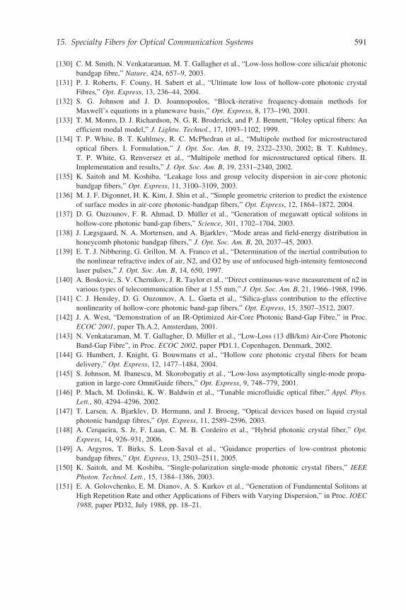
[130] C. M. Smith, N. Venkataraman, M. T. Gallagher et al., “Low-loss hollow-core silica/air photonic
bandgap fibre,” Nature, 424, 657–9, 2003.
[131] P. J. Roberts, F. Couny, H. Sabert et al., “Ultimate low loss of hollow-core photonic crystal
Fibres,” Opt. Express, 13, 236–44, 2004.
[132] S. G. Johnson and J. D. Joannopoulos, “Block-iterative frequency-domain methods for
Maxwell’s equations in a planewave basis,” Opt. Express, 8, 173–190, 2001.
[133] T. M. Monro, D. J. Richardson, N. G. R. Broderick, and P. J. Bennett, “Holey optical fibers: An
efficient modal model,” J. Lightw. Technol., 17, 1093–1102, 1999.
[134] T. P. White, B. T. Kuhlmey, R. C. McPhedran et al., “Multipole method for microstructured
optical fibers. I. Formulation,” J. Opt. Soc. Am. B, 19, 2322–2330, 2002; B. T. Kuhlmey,
T. P. White, G. Renversez et al., “Multipole method for microstructured optical fibers. II.
Implementation and results,” J. Opt. Soc. Am. B, 19, 2331–2340, 2002.
[135] K. Saitoh and M. Koshiba, “Leakage loss and group velocity dispersion in air-core photonic
bandgap fibers,” Opt. Express, 11, 3100–3109, 2003.
[136] M. J. F. Digonnet, H. K. Kim, J. Shin et al., “Simple geometric criterion to predict the existence
of surface modes in air-core photonic-bandgap fibers,” Opt. Express, 12, 1864–1872, 2004.
[137] D. G. Ouzounov, F. R. Ahmad, D. Muller et al., “Generation of megawatt optical solitons in
hollow-core photonic band-gap fibers,” Science, 301, 1702–1704, 2003.
[138] J. Lægsgaard, N. A. Mortensen, and A. Bjarklev, “Mode areas and field-energy distribution in
honeycomb photonic bandgap fibers,” J. Opt. Soc. Am. B, 20, 2037–45, 2003.
[139] E. T. J. Nibbering, G. Grillon, M. A. Franco et al., “Determination of the inertial contribution to
the nonlinear refractive index of air, N2, and O2 by use of unfocused high-intensity femtosecond
laser pulses,” J. Opt. Soc. Am. B, 14, 650, 1997.
[140] A. Boskovic, S. V. Chernikov, J. R. Taylor et al., “Direct continuous-wave measurement of n2 in
various types of telecommunication fiber at 1.55 mm,” J. Opt. Soc. Am. B, 21, 1966–1968, 1996.
[141] C. J. Hensley, D. G. Ouzounov, A. L. Gaeta et al., “Silica-glass contribution to the effective
nonlinearity of hollow-core photonic band-gap fibers,” Opt. Express, 15, 3507–3512, 2007.
[142] J. A. West, “Demonstration of an IR-Optimized Air-Core Photonic Band-Gap Fibre,” in Proc.
ECOC 2001, paper Th.A.2, Amsterdam, 2001.
[143] N. Venkataraman, M. T. Gallagher, D. Muller et al., “Low-Loss (13 dB/km) Air-Core Photonic
Band-Gap Fibre”, in Proc. ECOC 2002, paper PD1.1, Copenhagen, Denmark, 2002.
[144] G. Humbert, J. Knight, G. Bouwmans et al., “Hollow core photonic crystal fibers for beam
delivery,” Opt. Express, 12, 1477–1484, 2004.
[145] S. Johnson, M. Ibanescu, M. Skorobogatiy et al., “Low-loss asymptotically single-mode propa-
gation in large-core OmniGuide fibers,” Opt. Express, 9, 748–779, 2001.
[146] P. Mach, M. Dolinski, K. W. Baldwin et al., “Tunable microfluidic optical fiber,” Appl. Phys.
Lett., 80, 4294–4296, 2002.
[147] T. Larsen, A. Bjarklev, D. Hermann, and J. Broeng, “Optical devices based on liquid crystal
photonic bandgap fibres,” Opt. Express, 11, 2589–2596, 2003.
[148] A. Cerqueira, S. Jr, F. Luan, C. M. B. Cordeiro et al., “Hybrid photonic crystal fiber,” Opt.
Express, 14, 926–931, 2006.
[149] A. Argyros, T. Birks, S. Leon-Saval et al., “Guidance properties of low-contrast photonic
bandgap fibres,” Opt. Express, 13, 2503–2511, 2005.
[150] K. Saitoh, and M. Koshiba, “Single-polarization single-mode photonic crystal fibers,” IEEE
Photon. Technol. Lett., 15, 1384–1386, 2003.
[151] E. A. Golovchenko, E. M. Dianov, A. S. Kurkov et al., “Generation of Fundamental Solitons at
High Repetition Rate and other Applications of Fibers with Varying Dispersion,” in Proc. IOEC
1988, paper PD32, July 1988, pp. 18–21.
15. Specialty Fibers for Optical Communication Systems 591


