Embed Size (px)
Citation preview

Nanoscale
PAPER
aDepartment of Chemistry, PLASMANT R
Universiteitsplein 1, B-2610 Wilrijk-Antwer
ua.ac.bebIMEC, Kapeldreef 75, B-3001 Leuven, BelgicDepartment of Mechanical and Nuclear Eng
Park, Pennsylvania 16802, USA
Cite this: Nanoscale, 2013, 5, 719
Received 21st August 2012Accepted 13th November 2012
DOI: 10.1039/c2nr32387g
www.rsc.org/nanoscale
This journal is ª The Royal Society of
Reactive molecular dynamics simulations on SiO2-coated ultra-small Si-nanowires
Umedjon Khalilov,*a Geoffrey Pourtois,ab Annemie Bogaerts,a Adri C. T. van Duinc
and Erik C. Neytsa
The application of core–shell Si–SiO2 nanowires as nanoelectronic devices strongly depends on their
structure, which is difficult to tune precisely. In this work, we investigate the formation of the core–shell
nanowires at the atomic scale, by reactive molecular dynamics simulations. The occurrence of two
temperature-dependent oxidation mechanisms of ultra-small diameter Si-NWs is demonstrated. We
found that control over the Si-core radius and the SiOx (x # 2) oxide shell is possible by tuning the
growth temperature and the initial Si-NW diameter. Two different structures were obtained, i.e.,
ultrathin SiO2 silica nanowires at high temperature and Si core|ultrathin SiO2 silica nanowires at low
temperature. The transition temperature is found to linearly decrease with the nanowire curvature.
Finally, the interfacial stress is found to be responsible for self-limiting oxidation, depending on both the
initial Si-NW radius and the oxide growth temperature. These novel insights allow us to gain control
over the exact morphology and structure of the wires, as is needed for their application in nanoelectronics.
1 Introduction
Small-diameter (<10 nm) Si-NWs are potentially very attractivebecause of the quantization of the electronic structure.1,2 Nor-mally, such Si-NWs are obtained by oxidizing a large nanowireand subsequently removing the oxide layer.3–5 Such oxidationcan reduce the Si-NW diameter below the Bohr exciton radius toobtain visible photoluminescence due to quantum connementeffects. Interestingly, in this case, the band gap becomes sizedependent and increases as the size of the nanostructuredecreases, which indicates the possibility of developing Si-NWmaterials with a controllable band gap.1 For these and otherapplications to occur, obtaining an accurate control over theoxidation process is critical, which, however, is difficult toachieve.6 This requires a fundamental understanding of theoxidation mechanism of such small Si-NWs, which may besignicantly different from the existing mechanisms formicrometer sized Si-NWs.7,8
In microelectronics, self-limiting oxidation of Si nanowiresand spheres at the micrometer scale is of considerable concern,for instance for the design of metal–oxide–semiconductor(MOS) devices,2,8–14 such as wrap-gated15 and top-gated9 FETs orphotovoltaic cells.16 The oxidation behavior in this micrometerregime has been successfully modeled by Kao et al. for the case
esearch Group, University of Antwerp,
p, Belgium. E-mail: umedjon.khalilov@
um
ineering, Penn State University, University
Chemistry 2013
of wet Si-NW oxidation.8 However, the oxidation behaviorduring dry oxidation has not yet been properly investigated.Furthermore, such studies for ultra-small diameter Si-NWsbegin to appear only now.10
Once the self-limiting oxidation is established for small Si-NWs, the understanding of the stress dependence and the non-conservative nature of the oxidation process will be useful forcontrolling non-planar oxidation large scale integratedprocesses.11 The residual stress results in self- (or stress-)limiting oxidation when the strain energy at the interface islarger than the energy gain for the ambient oxygen to diffuseinto and oxidize the inner Si. Because the oxide should expandmore to accommodate the volume expansion in thinner Si-NWs,the self-limiting oxidation is more signicant in Si-NWs withsmaller diameters.11 According to the Kao model,8 compressivestresses normal to the Si|SiO2 interface reduce the interfacialreaction rate compared to a planar Si surface, whereas tensilestresses generated within the oxide shell reduce the effectiveoxide viscosity and enhance the oxygen diffusivity and solu-bility.6 However, such stress behavior may change in theoxidation of Si-NWs at the nanoscale, as the shape of thenanowire changes accordingly from circular to polygonal withincreasing curvature. Thus, stress results at the nanoscale maydisagree with the conclusions for Si-NW oxidation at the micro-scale due to this “curvature effect”.17
As mentioned above, the oxidation of ultra-small Si-NWs(<3 nm) has not yet been oen studied. Various characteristicsand processes, including dry oxidation mechanisms of small Si-NWs at different temperatures, self-limiting oxidation behavior,as well as the effects of size, temperature and stress on the
Nanoscale, 2013, 5, 719–725 | 719

Nanoscale Paper
oxidation process have not been properly studied yet. In thispaper we therefore focus on the oxidation of ultra-small Si-NWsin order to unravel these effects during and aer oxidation atthe atomic scale. We will specically discuss the ability tocontrol the Si-core radius and oxide sheath thickness by drythermal oxidation of (100) Si-NWs with initial diameters 1.0–3.0 nm in the temperature range of 300–1200 K.
Fig. 1 (a) Ideal (0 K) and thermalized (300 K and 1200 K) structures of Sinanowires (Si-NWs) with a diameter (d0) range of 1–3 nm. The indices 1 and 2indicate the {110} and {001}-type facets, respectively, which terminate thenanowires. (b) Top view of the facets in the Si-NW with d0 ¼ 2.5 nm at 0 K, 300 Kand 1200 K, respectively.
2 Computational detailsReaxFF potential
Oxidation of ultra-small Si-nanowires is studied using reactivemolecular dynamics (MD) simulations, employing the ReactiveForce Field (ReaxFF).18,19
ReaxFF is a classical force eld with parameters optimizedagainst both experimental and quantum mechanical (QM) datafor reaction energies, reaction barriers and congurationenergies as well as geometrical and structural data. ReaxFFaccurately simulates bond breaking and bond formationprocesses, commonly approaching QM accuracy. Thus, ReaxFFserves as a link between QM and empirical force elds.20 ReaxFFis based on the concept of the bond length–bond order/bondorder–bond energy relationship.21 The total system energyconsists of partial energy terms related to bond energies, lonepairs, undercoordination, overcoordination, valence andtorsion angles, conjugation, hydrogen bonding, as well as vander Waals and Coulomb interactions and so on.19
ReaxFF can currently describe tens of elements and theircombinations and its generic nature ensures its applicability toa wide range of materials and processes.22–32 In this work, we usethe force eld parameters employed by Buehler et al.33 Thisforce eld was trained extensively against both Si and SiO2
phases. Although SiOx (x < 2.0) suboxide phases were notincluded explicitly in this training set, our previous results on aplanar Si|SiO2 interface including these Si suboxide specieswere in good agreement with both experimental and DFTresults.34 A detailed description of the force eld can be foundelsewhere.19,33–35
Our choice for ReaxFF is based on the fact that it has beenparameterized to describe deformations and strains36,37
including bond breaking and formation, and its ability toaccurately describe the expansion of the crystal during the oxideformation process.38
Simulation details
In Fig. 1a, ideal (0 K) and thermalized (300 K and 1200 K)structures of the Si (100) nanowires (Si-NWs) with a diameter inthe range 1–3 nm are shown. In Fig. 1b, the top view of the {110}and {001} facets in the 2.5 nm diameter Si-NW is illustrated. Inour calculations, the nanowire diameter d0 corresponds to theaveraged distance between the center of mass of the wire andthe positions of the surface atoms in the radial direction in the(x,y) plane. A periodic boundary condition is applied along thez-axis, which corresponds to a unit cell length of 1 nm, to mimican innitely long nanowire. In reality, however, Si-NW havenite lengths, and longer than 1 nm. In order to test the “length
720 | Nanoscale, 2013, 5, 719–725
effect” we have performed a number of test calculations for1 nm diameter Si-NWs having different lengths (1 nm, 5 nm and10 nm). The results showed that the oxidation mechanism isidentical in all cases although the shapes are slightly different.Thus, we choose the 1 nm length Si-NW to minimize thecomputational time.
Prior to oxidation, the ideal Si(100) NWs are equilibrated at10 temperatures ranging from 300–1200 K in steps of 100 K for40 ps, using the isothermal–isobaric ensemble (i.e., NpTdynamics)39 with temperature and pressure coupling parame-ters of 0.1 ps and 5.0 ps, respectively. We employ the NpTensemble to ensure the generation of a zero-pressure structureat the desired temperature. To verify that the resulting structureis effectively relaxed at the desired temperature, the obtainedstructures are subsequently relaxed in the microcanonical NVEensemble for another 20 ps.
The structures at low temperatures (300–700 K) display both{110} and {001} facets, similar to the ideal samples as shown inFig. 1a. This suggested that the faceting affects the surfacereaction coefficient and subsequently the oxidation rate aswell.8,13,40,41 The shapes of the NW structures at high tempera-tures (800–1200 K), on the other hand, become more circular(see Fig. 1a). Si–Si bond-lengths and Si–Si–Si bond angles in allstructures are close to the experimental values for small Si(100)NWs.1
Oxygen impacts are performed as follows. Each incidentoxygen molecule (rO–O ¼ 0.121 nm) is randomly positioned at1 nm above the uppermost atom of the nanowire in the (x,y)plane. The O2 molecule is rotated randomly prior to impact.Every impact is followed for 10 ps, aer which the next impactstarts. The initial velocity vector of the incident molecule israndomized and its magnitude is set to the root-mean-squarevelocity corresponding to the oxidation temperature. During theimpacts, NpT dynamics are applied to allow for a volumeexpansion due to the oxidation process, as mentioned above.
Stress calculation details
During and aer oxidation, Cauchy atomic stresses werecalculated as the virial stress for pristine Si and the oxide
This journal is ª The Royal Society of Chemistry 2013

Fig. 2 Oxide formation and growth as a function of the O2 fluence in the 2 nmSi-NW at (a) low (300 K) and (b) high (1200 K) temperature, respectively. 1 MLcorresponds to 28 O2. Each structure is analyzed by the radial distribution of theSi-(sub)oxide components (black circles) and the O–O peroxyl bridges (red trian-gles). R is the radial distance from the centre of the Si-NW (i.e., R ¼ 0) to thenanowire atoms in the (x,y) plane. Here, Si, SiOx, (x > 2) and SiO2 correspond to thecrystalline silicon (or Si-core), non-stoichiometric oxide and amorphous silicaregions, respectively.
Paper Nanoscale
sheathed Si nanowires.42 The local stress is calculated bydividing the nanowire structure into small rectangular boxes.43
The stress tensor has 6 components for each atom and is storedas a 6-elements vector in rectangular Cartesian coordinates(x,y,z): sxx, syy, szz, syz, szx, and sxy. The local tensor of each iatom is dened as
si ¼24 sixx sixy sixz
siyx siyy siyz
sizx sizy sizz
35 ¼ 1
2U
XNk¼1
~F ik �~rik (1)
where U is the volume of the rectangular box, Fik is the vector ofthe force acting on atom i due to atom k, which are separatedfrom each other by the vector rik. N is the total number ofneighbors of atom i. The stresses in Cartesian coordinates aretransformed into cylindrical coordinates (r,q,z) as srr, sqq, szz,sqz, szr, and srq as follows:44
srr ¼ sxxcos2 qþ syysin
2qþ sxysin 2q
sqq ¼ sxxsin2qþ syycos
2q� sxysin 2q
szz ¼ szz
sqz ¼ syzcos q� szxsin q
szr ¼ syzsin qþ szxcos qsrq ¼ ðsyy � sxxÞsin qcos qþ sxycos 2q
(2)
where, cos q ¼ xr, sin q ¼ y
r, z ¼ z. The local stress in each box is
calculated by averaging the atomic stresses of the atomsincluded in the box.
For all stress calculations, the structures were rst equili-brated at 0.01 K using NpT dynamics, to remove the kineticenergy part from the stress calculation. Subsequently, the totalenergy was minimized using the steepest descent and conjugategradient techniques.45
3 Temperature-dependent oxidationmechanism
The dry oxidation behavior of a 2 nm diameter ultrasmall Si-NWis illustrated in Fig. 2, showing the oxide formation and growthprocess of the nanowire as a function of the O2 uence at (a) low(300 K) and (b) high (1200 K) temperature. The time evolution ofthe formation and growth of the oxygenated silicon is studied byobserving the variation of the silicon sub-oxide components(Sii+, i# 4) in order to easily compare with experiment (i.e., Si-2pphotoemission spectra46) and validate our results.
Prior to oxidation, only Si0 components are found, i.e., Si–Obonds do not exist in the Si-NW (Fig. 2, initial structures). Whenthe oxidation process starts, only Si1+ and Si2+ are initiallyformed. As the oxidation progresses, these are transformed intoSi3+ and subsequently into Si4+. Note that the notation usedcorresponds to the formal charge states and not to the actualatomic charges. Our calculations show that the Si1+, Si2+, andSi3+ fractions consecutively dominate in the initial oxidationstage. In this stage, the oxygenated Si-NW consists of crystallinesilicon (c-Si) and a SiOx region. Aer a uence of 2 ML (Fig. 2),the Si4+ suboxide species are also found on the oxidized Si-NWat low temperature, but not yet at high temperature. This meansthat the consecutive Si1+ / Si2+ / Si3+ / Si4+ conversion (i.e.,the appearance of a new silica layer) occurs much faster at low
This journal is ª The Royal Society of Chemistry 2013
temperature than at high temperature. Indeed, at low temper-ature, the penetrated O atoms or molecules cannot move deeperinto the nanowire due to the associated energy barrier and theSi–Si bonds convert relatively fast into Si–O bonds in the SiOx
region. When a stoichiometric (SiO2) oxide layer appears, thefraction of Si4+ components increases continuously and thefractions of the other suboxide components therefore decrease,as is clear from Fig. 2. This indicates the end of the initialoxidation stage. Our simulations show that this stage endsearlier at low temperature than at high temperature.
In the stage between 2 ML and 10 ML, the oxide growthprocess at low temperature is almost entirely stopped due to theenergy barrier, interfacial stresses and lowered diffusivity of thepenetrated oxygen species. This also leads to the appearance ofsome overcoordinated silicon (Si5+) species in the SiO2
region,10,47 albeit at low concentration (see Fig. 2a). The silicacontains a number of O–O peroxyl bonds as well (see Fig. 2, redtriangles),48 which also play a role in the appearance of Si5+ inthe oxygenated Si-NW. A similar effect was also suggested byDFT calculations by analyzing various defects during planar Sioxidation.34,47,49,50
Starting from 10 ML, the number of peroxyl linkages andve-fold coordinated silicon atoms increases and they spread inthe whole silica region. This indicates that Si-NW oxidation isonly continued by diffusing oxygen species. Therefore, theduration of this process is much longer than the initial oxida-tion stage. Indeed, the oxidation rate not only depends on thesurface reaction coefficient, but also on the transfer and diffu-sion coefficients. Such an oxidation behavior is also explainedin depth by Kao and co-workers in their micro-scale model.8
Furthermore, distribution of the O–O peroxyl bridges in the Si-NW at low temperature indicated that oxidation continues in
Nanoscale, 2013, 5, 719–725 | 721

Nanoscale Paper
the slow oxidation stage (see 10 and 40 ML in Fig. 2a). Such anoxidation behaviour was not reported in wet oxidation of Si-NWs.8 A similar oxidation behaviour is also observed at hightemperature (40 ML, Fig. 2b), albeit its contribution is smallcompared with the low temperature case. Although the oxidegrowth continues, the Si-core radius remains constant at lowtemperature aer 40 ML. At high temperature, some oxygenspecies penetrate into the Si-NW center already at 10 ML. In thenal oxidized nanowire (Fig. 2b, 100 ML), all Si atoms are in theSi4+ oxidation state and all O–O peroxyl bridges disappear. Onthe other hand, at low temperature, all Si-suboxide components(including some Si5+) can be found in the nal structure aer100 ML, as is illustrated in Fig. 2a. However, such intermediatestructures, i.e., overcoordinated Si atoms and peroxyl linkages,are only found on the silica surface, and not in the whole silicaregion, indicating that the oxide growth by diffusing oxygenspecies has entirely stopped.
Finally, at the end of the oxidation process, two differentstructures are obtained (Fig. 2, nal structures). The overallspread in the radial distribution function (RDF), angle andmass density distributions conrms that the initially crystallinesilicon (c-Si) nanowire converts into either a silicon-silica (c-Si|SiOx|a-SiO2) nanowire at a low temperature (300 K) or anamorphous silica (a-SiO2) nanowire at a high temperature(1200 K). This was also reported in our previous work, as well asin the literature.10,51 The formation of the structure obtained atlow temperature can be explained by self-limiting oxidation,8,11
as will be further explained below.
4 Ultra-small Si|SiOx|SiO2 nanowires
As mentioned in the previous section, and as illustrated inFig. 3, two types of nanostructures are ultimately obtained, i.e.,c-Si|SiOx|a-SiO2 (typical at low temperatures) and a-SiO2 nano-wires (typical at the higher temperatures). Only the 1 nmdiameter Si-NW (not shown in Fig. 3) completely converts intothe a-SiO2 nanowire at all temperatures. In Fig. 3a, all nallyobtained core shell c-Si|SiOx|a-SiO2 structures are shown. Attemperatures above 800 K, all obtained structures are fullyamorphous and are therefore not shown. The gure illustrates
Fig. 3 (a) The c-Si|SiOx|a-SiO2 nanowires with initial diameters in the range 1.5–3 nm after oxidation at T ¼ 300–800 K. (b) Final radii of Si-core (r) and Si-NW (R),compared with theoretical calculations derived from eqn (3).
722 | Nanoscale, 2013, 5, 719–725
that both the Si-core radius (r) as well as the Si-NW radius (R)depend on the d0 diameter and inversely depend on the
oxidation (or oxide growth) temperature T, i.e., rðor RÞe d0T. We
found that the maximum radius of the Si-core is about 0.26 nm,0.46 nm, 0.65 nm and 0.91 nm for 1.5, 2, 2.5 and 3 nm diameterSi-NWs, respectively, at 300 K. Due to the increasing diffusivityand mobility of the penetrated oxygen atoms, the core radiusdrops with rising temperature. While the growth temperatureincreases, the Si-core radius decreases to zero (r / 0) andconsequently the nanowire converts into a pure SiOx (x # 2)nanowire at a certain “transition temperature” (Ttrans). Thus, fora given nanowire diameter, Ttrans is the temperature abovewhich amorphous silica (a-SiO2) is obtained, and below whichcore–shell c-Si|SiOx|a-SiO2 nanowires are obtained. From Fig. 3ait can be seen that Ttrans is roughly equal to 500 K, 600 K, 700 Kand 800 K for Si-NWs with diameters of 1.5 nm, 2 nm, 2.5 nmand 3 nm, respectively. This clearly demonstrates that controlover the Si-core radius is possible by selecting the appropriateinitial diameter of the Si-NW and the growth temperature.
The nal radii of the c-Si|SiOx|a-SiO2 nanowires, as obtainedin our MD calculations, can be compared with a theoreticalderivation, to which also most experimentalists compare theirresults:9,40,51
p�R2 � r2
�L� p
�R0
2 � r02�L ¼ USiO2
USi
p�r0
2 � r2�L (3)
where r0, r and R0, R are the initial and nal radii of the Si-coreand oxidized Si-NW, respectively; L is the Si-NW length; USiO2
isthe molecular volume of SiO2 (�45 A3) and USi is the atomicvolume of Si (20 A3). Prior to oxidation, initially r0 ¼ R0. From(3), the following formula including this initial condition can beobtained:
R ¼ffiffiffiffiffiffiffiffiffiffiffiffiffiffiffiffiffiffiffiffiffiffiffiffiffiffiffiffiffiffiffiffiffi2:25r02 � 1:25r2
p(4)
The relationship between the nal Si-NW (R) and Si-core (r)radii for partially oxidized structures can be calculated bymeansof this formula. The results are presented in Fig. 3b (grey curves).It can be seen in the gure that most of our MD results are fairlyclose to this theoretical calculation. Furthermore, this indicatesthat at low temperature, the oxidation process does not stronglydepend on the diffusion coefficient and is only a function of thesurface reaction rate, which depends on the normal stress ratherthan on the temperature. Especially in the cases above 2 nmdiameter, this effect clearly appears: at all temperatures belowthe transition temperature, the diamonds (d0 ¼ 2.5 nm) orpentagons (d0 ¼ 3 nm) are close to each other, close to the lowerdotted line, indicating that the oxidation hardly changesbetween these temperatures. Increasing the temperature toabove the transition temperature, however, results in a strongincrease in the oxidation, as indicated by the datapoints lyingclose to theupper dotted line.Note that this effect is not observedin the Si-NWs with a higher curvature (d0 < 2.5 nm).
Indeed, it was previously suggested that compressive stressesat the Si|SiO2 interface signicantly slow down the reactionrate,8,11–13 and furthermore, that a compressive pressure in SiO2
can reduce the oxidant diffusion and transport.12
This journal is ª The Royal Society of Chemistry 2013
Paper Nanoscale
5 Stress evolutions during self-limitingoxidation
We rst calculated the stresses (normal or radial srr, tangentialsqq and axial szz) in the pristine Si-NWs. Our calculations showthat although all pre-oxidation stresses change depending onthe crystal orientation and nanowire curvature, their values arevery small and close to the previously suggested values.8
Although the average values of the srr and sqq stresses arecompressive, their contributions to reducing the Si–O reactionrate are negligible.
In Si-NW oxidation, two key factors can be discerned: (1)oxygen diffusion in the SiOx (x # 2) oxide region, characterizedby the diffusion constant D; and (2) reaction with the Si-core,characterized by the reaction rate constant ks.8 These twoparameters also strongly depend on the hydrostatic pressure p(i.e., the obtained oxide can be considered as a uid with highviscosity8) and the normal stress srr at a given temperature,respectively. According to uid mechanics, the pressure is equalto the average total srr on a control volume in the uid and it is
found as p ¼ � 12ðsrr þ sqqÞ.52
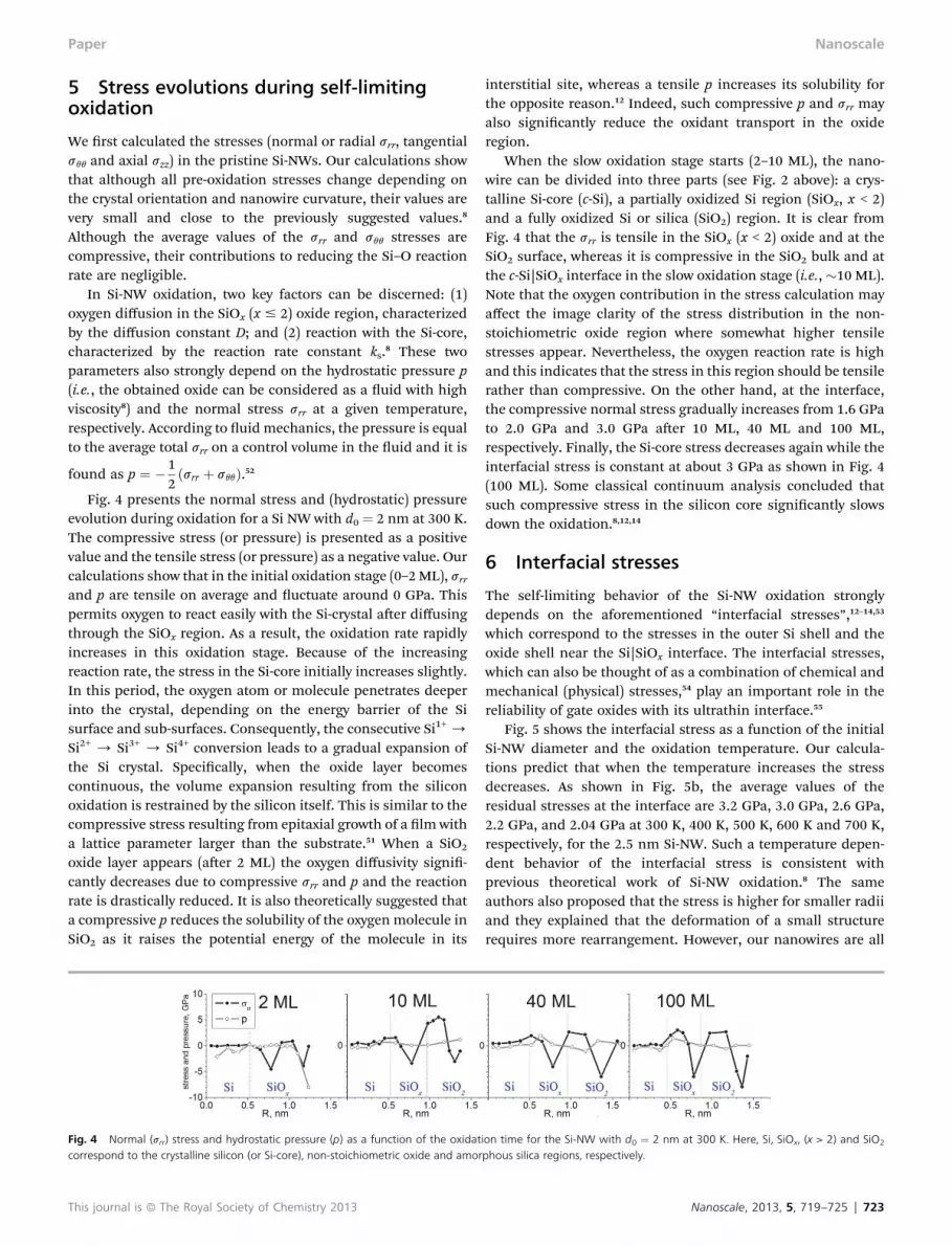
Fig. 4 presents the normal stress and (hydrostatic) pressureevolution during oxidation for a Si NW with d0 ¼ 2 nm at 300 K.The compressive stress (or pressure) is presented as a positivevalue and the tensile stress (or pressure) as a negative value. Ourcalculations show that in the initial oxidation stage (0–2ML), srrand p are tensile on average and uctuate around 0 GPa. Thispermits oxygen to react easily with the Si-crystal aer diffusingthrough the SiOx region. As a result, the oxidation rate rapidlyincreases in this oxidation stage. Because of the increasingreaction rate, the stress in the Si-core initially increases slightly.In this period, the oxygen atom or molecule penetrates deeperinto the crystal, depending on the energy barrier of the Sisurface and sub-surfaces. Consequently, the consecutive Si1+ /Si2+ / Si3+ / Si4+ conversion leads to a gradual expansion ofthe Si crystal. Specically, when the oxide layer becomescontinuous, the volume expansion resulting from the siliconoxidation is restrained by the silicon itself. This is similar to thecompressive stress resulting from epitaxial growth of a lm witha lattice parameter larger than the substrate.51 When a SiO2
oxide layer appears (aer 2 ML) the oxygen diffusivity signi-cantly decreases due to compressive srr and p and the reactionrate is drastically reduced. It is also theoretically suggested thata compressive p reduces the solubility of the oxygen molecule inSiO2 as it raises the potential energy of the molecule in its
Fig. 4 Normal (srr) stress and hydrostatic pressure (p) as a function of the oxidatcorrespond to the crystalline silicon (or Si-core), non-stoichiometric oxide and amor
This journal is ª The Royal Society of Chemistry 2013
interstitial site, whereas a tensile p increases its solubility forthe opposite reason.12 Indeed, such compressive p and srr mayalso signicantly reduce the oxidant transport in the oxideregion.
When the slow oxidation stage starts (2–10 ML), the nano-wire can be divided into three parts (see Fig. 2 above): a crys-talline Si-core (c-Si), a partially oxidized Si region (SiOx, x < 2)and a fully oxidized Si or silica (SiO2) region. It is clear fromFig. 4 that the srr is tensile in the SiOx (x < 2) oxide and at theSiO2 surface, whereas it is compressive in the SiO2 bulk and atthe c-Si|SiOx interface in the slow oxidation stage (i.e., �10 ML).Note that the oxygen contribution in the stress calculation mayaffect the image clarity of the stress distribution in the non-stoichiometric oxide region where somewhat higher tensilestresses appear. Nevertheless, the oxygen reaction rate is highand this indicates that the stress in this region should be tensilerather than compressive. On the other hand, at the interface,the compressive normal stress gradually increases from 1.6 GPato 2.0 GPa and 3.0 GPa aer 10 ML, 40 ML and 100 ML,respectively. Finally, the Si-core stress decreases again while theinterfacial stress is constant at about 3 GPa as shown in Fig. 4(100 ML). Some classical continuum analysis concluded thatsuch compressive stress in the silicon core signicantly slowsdown the oxidation.8,12,14
6 Interfacial stresses
The self-limiting behavior of the Si-NW oxidation stronglydepends on the aforementioned “interfacial stresses”,12–14,53
which correspond to the stresses in the outer Si shell and theoxide shell near the Si|SiOx interface. The interfacial stresses,which can also be thought of as a combination of chemical andmechanical (physical) stresses,54 play an important role in thereliability of gate oxides with its ultrathin interface.55
Fig. 5 shows the interfacial stress as a function of the initialSi-NW diameter and the oxidation temperature. Our calcula-tions predict that when the temperature increases the stressdecreases. As shown in Fig. 5b, the average values of theresidual stresses at the interface are 3.2 GPa, 3.0 GPa, 2.6 GPa,2.2 GPa, and 2.04 GPa at 300 K, 400 K, 500 K, 600 K and 700 K,respectively, for the 2.5 nm Si-NW. Such a temperature depen-dent behavior of the interfacial stress is consistent withprevious theoretical work of Si-NW oxidation.8 The sameauthors also proposed that the stress is higher for smaller radiiand they explained that the deformation of a small structurerequires more rearrangement. However, our nanowires are all
ion time for the Si-NW with d0 ¼ 2 nm at 300 K. Here, Si, SiOx, (x > 2) and SiO2
phous silica regions, respectively.
Nanoscale, 2013, 5, 719–725 | 723

Fig. 5 Averaged radial (normal) srr stresses at the Si|SiO2 interface of the finaloxidized Si-NW structure as a function of (a) the curvature and (b) oxide growthtemperature. (c) The interfacial srr stress on the x–y plane for a Si-NW with d0 ¼ 3nm at 300 K. The (0, 0) position corresponds to the Si-NW center.
Nanoscale Paper
very small and the obtained results are opposite to this theo-retical suggestion. Indeed, our calculations predict that the1.5 nm diameter Si-NW exhibits a somewhat smaller compres-sive stress than the other nanowires (Fig. 5a). To be exact, theaveraged interfacial stress of the NWs at 300 K is calculated tobe 2.9 GPa, 3.0 GPa, 3.2 GPa, and 3.5 GPa for the NWs with1.5 nm, 2 nm, 2.5 nm and 3 nm diameter, respectively. Thisphenomenon of a residual compressive stress decreasing withrising curvature was also reported by Kim et al.17 Followingthese authors, the non-oxidized Si-core of smaller Si-NWs withdiameters in the sub-10 nm range deforms more to compensatefor the volume expansion of the surface oxide layer, resulting ina smaller compressive stress. Furthermore, we also suggest thatcrystal orientation effects may play a role to develop thisphenomenon.
The distribution of interfacial stresses around the Si-core inthe (x,y) plane is also presented in Fig. 5c. As shown in thegure, the compressive interfacial stresses at room temperatureare signicantly higher than the stresses of its Si-core. Suchcompressive stresses signicantly reduce the oxygen reactionwith Si near the planar Si|SiO2 interface, which was investigatedusing high-resolution transmission electron microscopy(HRTEM) analysis.56 Indeed, these residual stresses are rela-tively high at a low temperature (e.g., 300 K) in ultra-small Si-NWs and therefore their effect is signicant in self-limitingoxidation.10,11 Thus, it is observed from our calculations thataccurate control of the interfacial stress by choosing a suitabletemperature and Si-NW diameter can lead to accurate controlover the Si-core radius at the nanoscale.
7 Conclusions
Oxidationof ultra-small Si nanowireswith initial diameters in therange 1 nm to 3 nm was studied using reactive moleculardynamics. We studied the temperature-dependent dry oxidationmechanism of small Si-NWs at low (300 K) and high (1200 K)temperatures. The oxidation mechanism is discussed incomparison to wet oxidation of micrometer sized Si-NWs andothermechanismsofplanar Si oxidation.DiffusionofO–Obridgelinkages is also discussed. Although their contribution is small,they may play a role in a diffusion-dependent oxidation process.
724 | Nanoscale, 2013, 5, 719–725
At the end of the oxidation two types of structures arefound: at low temperatures, c-Si|SiOx|a-SiO2 nanowires areformed, while a-SiO2 nanowires are formed at higher temper-atures. The transition temperature between both regimes wasfound to increase with the NW diameter. Indeed, for the 1.5nm, 2 nm, 2.5 nm and 3 nm diameter Si-NWs, the transitiontemperature was found to be about 500 K, 600 K, 700 K and800 K, respectively. The nal radii of the c-Si|SiOx|a-SiO2
nanowires are close to the theoretically suggested radii. Ourcalculations predict for the partially oxidized c-Si|SiOx|a-SiO2
nanowires that the Si-core (c-Si) and the total nanowire radiusdepend on the initial Si-NW diameter and inversely depend onthe oxidation temperature.
Stress calculations were also performed to study the self-limiting nature of the oxidation of these ultra-small nanowires.It is found that a compressive pressure and stress may signi-cantly reduce the oxidant transport in the oxide region and itsreaction with the Si-core. Stresses at the interface were alsoanalyzed. Specically, when the temperature increases, theinterfacial stresses decrease. This is consistent with previoustheoretical work. However, we also found that the compressiveinterfacial stresses decrease with increasing curvature for the 1–3 nm Si-NWs investigated, which is in contrast to the theoreticalsuggestions for Si-NWs at the micro-scale.
Generally, we can conclude from our simulations that anaccurate control over the interfacial stress by choosing a suit-able oxidation temperature and a Si-NW diameter can lead to aprecise control over the Si-core radius at the nanoscale regime.
Acknowledgements
U. Khalilov acknowledges imec for nancial support. G. Pour-tois acknowledges support from the Future and EmergingTechnologies (FET) program within the 7th FrameworkProgram for Research of the European Commission under theFET-Open grant number 270749- 2DNANOLATTICES. A. C. T.van Duin acknowledges funding from the Air Force Office ofScientic Research (AFOSR) under Grant no. FA9550-10-1-0563.The authors also gratefully acknowledge nancial support fromthe Prime Minister's Office through IAP VI. This work wascarried out using the Turing HPC infrastructure at the CalcUAcore facility of the Universiteit Antwerpen (UA), a division of theFlemish Supercomputer Center VSC, funded by the HerculesFoundation, the Flemish Government (department EWI) andthe UA.
References
1 D. D. D. Ma, C. S. Lee, F. C. K. Au, S. Y. Tong and S. T. Lee,Science, 2003, 299, 1874.
2 K. Trivedi, H. Yuk, H. C. Floresca, M. J. Kim andW. Hu, NanoLett., 2011, 11, 1412–1417.
3 J. S. Judge, J. Electrochem. Soc., 1971, 118, 1772–1775.4 P. A. M. van der Heide, M. J. Baan Hofman and H. J. Ronde, J.Vac. Sci. Technol., A, 1989, 7, 1719–1723.
5 J. Magyar, A. Sklyarov, K. Mikaylichenko and V. Yakovlev,Appl. Surf. Sci., 2003, 207, 306–313.
This journal is ª The Royal Society of Chemistry 2013

Paper Nanoscale
6 S. Krylyuk, A. V. Davydov, I. Levin, A. Motayed andM. D. Vaudin, Appl. Phys. Lett., 2009, 94, 063113.
7 B. E. Deal and A. S. Grove, J. Appl. Phys., 1965, 36, 3770–3778.
8 D.-B. Kao, J. P. McVittie, W. D. Nix and C. K. Saraswat, IEEETrans. Electron Devices, 1988, 35, 25–37.
9 B. Liu, Y. Wang, T. Ho, K.-K. Lew, S. M. Eichfeld,J. M. Redwing, T. S. Mayer and S. E. Mohney, J. Vac. Sci.Technol., A, 2008, 26, 370.
10 U. Khalilov, G. Pourtois, A. C. T. van Duin and E. C. Neyts,Chem. Mater., 2012, 24, 2141–2147.
11 H. I. Liu, D. K. Biegelsen, N. M. Johnson, F. A. Ponce andR. F. W. Pease, J. Vac. Sci. Technol., B, 1993, 11, 6.
12 J. Dalla Torre, J.-L. Bocquet, Y. Limoge, J.-P. Crocombette,E. Adam and G. J. Martin, J. Appl. Phys., 2002, 92, 2.
13 P.-F. Fazzini, C. Bonafos, A. Claverie, A. Hubert, T. Ernst andM. Respaud, J. Appl. Phys., 2011, 110, 033524.
14 Y. Chen, Modeling of the Self-Limiting Oxidation forNanofabrication of Si, in Technical Proceedings of the ThirdInternational Conference on Modeling and Simulation ofMicrosystem, Nano Science and Technology Institute:Austin, TX, San Diego, CA, March 27–29, 2000, vol. 2000,pp. 56–58.
15 J. Goldberger, A. I. Hochbaum, R. Fan and P. Yang, NanoLett., 2006, 6, 2006.
16 M. Konagai, Jpn. J. Appl. Phys., 2011, 50, 030001.17 B.-H. Kim, M. A. Pamungkas, M. Park, G. Kim, K.-R. Lee and
Y.-C. Chung, Appl. Phys. Lett., 2011, 99, 143115.18 A. C. T. van Duin, S. Dasgupta, F. Lorant and W. A. Goddard
III, J. Phys. Chem. A, 2001, 105, 9396–9409.19 A. C. T. van Duin, A. Strachan, S. Stewman, Q. Zhang, X. Xu
and W. A. Goddard III, J. Phys. Chem. A, 2003, 107, 3803–3811.
20 M. J. Buehler, J. Comput. Theor. Nanosci., 2006, 3, 603–623.21 G. C. Abell, Phys. Rev. B: Condens. Matter Mater. Phys., 1985,
31, 6184–6196.22 E. C. Neyts, Y. Shibuta, A. C. T. van Duin and A. Bogaerts, ACS
Nano, 2010, 4, 6665–6672.23 E. C. Neyts, A. C. T. van Duin and A. Bogaerts, J. Am. Chem.
Soc., 2011, 133, 17225–17231.24 E. C. Neyts, A. C. T. van Duin and A. Bogaerts, J. Am. Chem.
Soc., 2012, 134, 1256–1260.25 P. Valentini, T. E. Schwartzentruber and I. Cozmuta, J. Chem.
Phys., 2010, 133, 084703.26 J. E. Mueller, A. C. T. van Duin andW. A. Goddard III, J. Phys.
Chem. C, 2010, 114, 5675–5685.27 N. Ning, F. Calvo, A. C. T. van Duin, D. J. Wales and H. Vach,
J. Phys. Chem. C, 2009, 113, 518–523.28 J. C. Fogarty, H. M. Aktulga, A. Y. Grama, A. C. T. van Duin
and S. Pandit, J. Chem. Phys., 2010, 132, 174704.29 K. Chenoweth, A. C. T. van Duin and W. A. Goddard III, J.
Phys. Chem. A, 2008, 112, 1040–1053.30 O. Rahaman, A. C. T. van Duin, W. A. Goddard III and
D. J. Doren, J. Phys. Chem. B, 2011, 115, 249–261.
This journal is ª The Royal Society of Chemistry 2013
31 S. Monti, A. C. T. van Duin, S.-Y. Kim and V. Barone, J. Phys.Chem. C, 2012, 116, 5141–5150.
32 R. M. Abolfath, A. C. T. van Duin and T. Brabec, J. Phys.Chem. A, 2011, 115, 11045.
33 M. J. Buehler, A. C. T. van Duin and W. A. Goddard III, Phys.Rev. Lett., 2006, 96, 095505.
34 U. Khalilov, E. C. Neyts, G. Pourtois and A. C. T. van Duin, J.Phys. Chem. C, 2011, 115, 24839–24848.
35 A. C. T. van Duin, J. M. A. Baas and B. van de Graaf, J. Chem.Soc., Faraday Trans., 1994, 90, 2881–2895.
36 Y. Park, H. M. Atkulga, A. Grama and A. Strachan, J. Appl.Phys., 2009, 106, 034304.
37 P. Ganster, G. Treglia and A. Saul, Phys. Rev. B: Condens.Matter Mater. Phys., 2010, 81, 045315.
38 A. P. Garcia, D. Sen andM. J. Buehler,Metall. Mater. Trans. A,2011, 42, 3889–3897.
39 H. J. C. Berendsen, J. P. M. Postma, W. F. van Gunsteren,A. DiNola and J. R. Haak, J. Chem. Phys., 1984, 81, 3684–3690.
40 D. Shir, B. Z. Liu, A. M. Mohammad, K. K. Lew andS. E. Mohney, J. Vac. Sci. Technol., B, 2006, 24, 1333.
41 J. L. Liu, Y. Lu, Y. Shi, S. L. Gu, R. L. Jiang, F. Wang, H. M. Buand R. L. Zheng, Phys. Status Solidi A, 1998, 168, 441.
42 I. Daruka, A.-L. Barabasi, S. J. Zhou, T. C. Germann,P. S. Lomdahl and A. R. Bishop, Phys. Rev. B: Condens.Matter Mater. Phys., 1999, 60, R2150–R2153.
43 H. Ohta, T. Watanabe and I. Ohdomari, Jpn. J. Appl. Phys.,2007, 46, 3277–3282.
44 I. Okumura, On the Stress Field in Orthogonal CurvilinearCoordinates, Memoirs of the Kitami Institute ofTechnology, 2000, vol. 32, pp. 51–65.
45 A. R. Leach, Molecular Modeling: Principles and Application,Prentice Hall, England, 2nd edn, 2001, p. 303.
46 A. Yoshigoe and Y. Teraoka, Surf. Sci., 2003, 532–535, 690–697.
47 K.-O. Ng and D. Vanderbilt, Phys. Rev. B: Condens. MatterMater. Phys., 1999, 59, 10132–10137.
48 A. M. Stoneham, M. A. Szymanski and A. L. Shluger, Phys.Rev. B: Condens. Matter Mater. Phys., 2001, 63, 221304.
49 G. F. Cerofolini, D. Mascolo and M. O. Vlad, J. Appl. Phys.,2006, 100, 054308.
50 D. R. Hamann, Phys. Rev. Lett., 1998, 81, 3447–3450.51 C. C. Buttner and M. Zacharias, Appl. Phys. Lett., 2006, 89,
263106.52 M. M. Denn, Process Fluid Mechanics, Prentice-Hall,
Englewood Cliffs, NJ, 1980.53 U. Khalilov, G. Pourtois, A. C. T. van Duin and E. C. Neyts, J.
Phys. Chem. C, 2012, 116, 8649–8656.54 A. Korkin, J. C. Greer, G. Bersuker, V. V. Karasiev and
R. J. Bartlett, Phys. Rev. B: Condens. Matter Mater. Phys.,2006, 73, 165312.
55 T.-C. Yang and K. C. Saraswat, IEEE Trans. Electron Devices,2000, 47, 746–755.
56 P. Donnadieu, E. Blanquet, N. Jakse and P. Mur, Appl. Phys.Lett., 2004, 85, 5574.
Nanoscale, 2013, 5, 719–725 | 725


