Embed Size (px)
Citation preview
Resonant Reset Forward Topologies for Low Output Voltage On Board Converters
J.A. Cobos, 0. Garcia, J. Sebastian, J. Uceda
Universidad PolitCcnica de Madrid ETS . Ing . Industriales-Electrhica
c/ JosC GutiCrrez Abascal,2 28006 Madrid SPAIN Phone: 34-1- 411 75 17 Fax: 34-1- 564 59 66
ABSTRACT : The minimization of sue and losses are the main goals in the design of high power density and low output voltage on board dJdc converters. Forward topology with resonant reset combines the simplicity of i& power stage with the feasibility to implement self driven synchronous rectification. Several operation modes for this topology are proposed and analyzed in this paper: fiedfrequency PWMandconstant off-time variablefrequency, with and without zero voltage switching (ZVS). Design guidelines and experimental results are also provided for 3.3V output voltage converters, featuring eflciencies up to 90%.
I. INTRODUCTION
The main requirements for on board converters to be used in computer and telecommunication systems are their size and efficiency. A simple power stage capable to operate at high switching frequencies with very high efficiency, even with low output voltage, would be the best choice for this kind of applications.
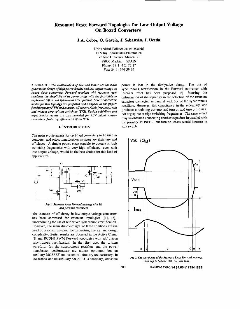
n:l
'r Fig 1. Resonant Reset Forward topology with SR
and parasitic reactances
The increase of efficiency in low output voltage converters has been addressed for resonant topologies ([l], [2]), incorporating the use of self driven synchronous rectification. However, the main disadvantages of these solutions are the need of resonant devices, the circulating energy, and design complexity. Better results are obtained in the Active Clamp [3] and RCD[4] PWM Forward topologies with self driven synchronous rectification. In the first one, the driving waveform for the synchronous rectifiers and the power transformer performance are almost optimum, but an auxiliary MOSFET and its control circuitry are necessary. In the second one no auxiliary MOSFET is necessary, but some
703
power is lost in the dissipative clamp. The use of synchronous rectification in the Forward converter with resonant reset has been proposed [6] , focusing the optimization of the topology in the selection of the resonant capacitor connected in parallel with one of the synchronous rectifiers. However, this capacitance in the secondary side produces circulating currents and turn on and turn off losses, not negligible at high switching frequencies. The same effect may be obtained connecting another capacitor in parallel with the primary MOSFET, but turn on losses would increase in this switch.
(QM)
Fig 2. Key waveform of the Resonant Reset Forward topology. From top to bottom: VDS, Vsec and Imag.
0-7803-1 456-5194 $4.00 0 1994 IEEE
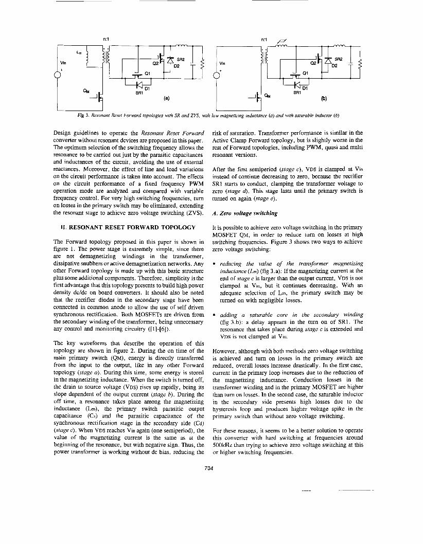
n:l n:l @
0'
Fig 3. Resonant Reset Forward topologies with SR and ZVS, with
Design guidelines to operate the Resonant Reset Forward converter without resonant devices are proposed in this paper. The optimum selection of the switching frequency allows the resonance to be carried out just by the parasitic capacitances and inductances of the circuit, avoiding the use of external reactances. Moreover, the effect of line and load variations on the circuit performance is taken into account. The effects on the circuit performance of a fixed frequency PWM operation mode are analyzed and compared with variable frequency control. For very high switching frequencies, turn on losses in the primary switch may be eliminated, extending the resonant stage to achieve zero voltage switching (ZVS).
11. RESONANT RESET FORWARD TOPOLOGY
The Forward topology proposed in this paper is shown in figure 1. The power stage is extremely simple, since there are not demagnetizing windings in the transformer, dissipative snubbers or active demagnetization networks. Any other Forward topology is made up with this basic structure plus some additional components. Therefore, simplicity is the first advantage that this topology presents to build high power density dc/dc on board converters. It should also be noted that the rectifier diodes in the secondary stage have been connected in common anode to allow the use of self driven synchronous rectification. Both MOSFETs are driven from the secondary winding of the transformer, being unnecessary any control and monitoring circuitry ([ 11-[6]).
The key waveforms that describe the operation of this topology are shown in figure 2. During the on time of the main primary switch (QM), energy is directly transferred from the input to the output, like in any other Forward topology (stage a). During this time, some energy is stored in the magnetizing inductance. When the switch is turned off, the drain to source voltage (VDS) rises up rapidly, being its slope dependent of the output current (stage 6). During the off time, a resonance takes place among the magnetizing inductance (Lm), the primary switch parasitic output capacitance (Cs) and the parasitic capacitance of the synchronous rectification stage in the secondary side (Cd) (stage c). When VDS reaches Vin again (one semiperiod), the value of the magnetizing current is the same as at the beginning of the resonance, but with negative sign. Thus, the power transformer is working without dc bias, reducing the
~~
low magnetizing inductance (a) and with saturable inductor (b)
risk of saturation. Transformer performance is similar in the Active Clamp Forward topology, but is slightly worse in the rest of Forward topologies, including PWM, quasi and multi resonant versions.
After the first semiperiod (stage c) , VDS is clamped at Vin instead of continue decreasing to zero, because the rectifier SR1 starts to conduct, clamping the transformer voltage to zero (stage 4. This stage lasts until the primary switch is turned on again (stage e).
A . Zero voltage switching
It is possible to achieve zero voltage switching in the primary MOSFET QM, in order to reduce tum on losses at high switching frequencies. Figure 3 shows two ways to achieve zero voltage switching:
reducing the value of the transformer magnetizing inductance (Lm) (fig 3.a): If the magnetizing current at the end of stage c is larger than the output current, VDS is not clamped at Vin, but it continues decreasing. With an adequate selection of Lm, the primary switch may be turned on with negligible losses.
adding a saturable core in the secondary winding (fig 3.b): a delay appears in the turn on of SR1. The resonance that takes place during stage c is extended and VDS is not clamped at Vin.
However, although with both methods zero voltage switching is achieved and turn on losses in the primary switch are reduced, overall losses increase drastically. In the first case, current in the primary loop increases due to the reduction of the magnetizing inductance. Conduction losses in the transformer winding and in the primary MOSFET are higher than turn on losses. In the second case, the saturable inductor in the secondary side presents high losses due to the hysteresis loop and produces higher voltage spike in the primary switch than without zero voltage switching.
For these reasons, it seems to be a better solution to operate this converter with hard switching at frequencies around SOOkHz than trying to achieve zero voltage switching at this or higher switching frequencies.
704
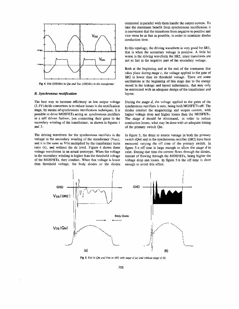
connected in parallel with them handle the output current. To take the maximum benefit from synchronous rectification it is convenient that the transitions from negative to positive and vice versa be as fast as possible, in order to minimize diodes conduction time.
In this topology, the driving waveform is very good for SR1, that is when the secondary voltage is positive. A little bit worse is the driving waveform for SR2, since transitions are not so fast in the negative part of the secondary voltage.
Both at the beginning and at the end of the resonance that takes place during stage c , the voltage applied to the gate of SR2 is lower than its threshold voltage. There are some oscillations at the beginning of this stage due to the energy stored in the leakage and layout inductances, that may only be minimized with an adequate design of the transformer and
Fig 4. VDS (5OVdiv) in QM and Vsec (IOVdiv) in the transformer
B. Synchronous rectification layout.
The best way to increase efficiency in low output voltage (3.3V) dc/dc converters is to reduce losses in the rectification stage, by means of synchronous rectification techniques. It is possible to drive MOSFETs acting as synchronous rectifiers in a self driven fashion, just connecting their gates to the secondary winding of the transformer, as shown in figures 1 and 3.
During the stage d , the voltage applied to the gates of the synchronous rectifiers is zero, being both MOSFETs off. The diodes conduct the magnetizing and output current, with higher voltage drop and higher losses than the MOSFETs. The stage d should be eliminated, in order to reduce conduction losses, what may be done with an adequate timing of the primary switch QM.
The driving waveform for the synchronous rectifiers is the voltage in the secondary winding of the transformer (Vsec), and it is the same as VDS multiplied by the transformer turns ratio (n), and without the dc level. Figure 4 shows these voltage waveforms in an actual prototype. When the voltage in the secondary winding is higher than the threshold voltage of the MOSFETs, they conduct. When that voltage is lower than threshold voltage, the body diodes or the diodes
In figure 5, the drain to source voltage in both the primary switch (QM) and in the synchronous rectifier (SR2) have been measured varying the off time of the primary switch. In figure 5.a off time is large enough to allow the stage d to exist. During that time the current flows through the diodes, instead of flowing through the MOSFETs, being higher the voltage drop and losses. In figure 5.b the off time is short enough to avoid this effect.
Fig 5. VDS in QM and VDS in SR2 with stage d (a) and without stage d (b)
705
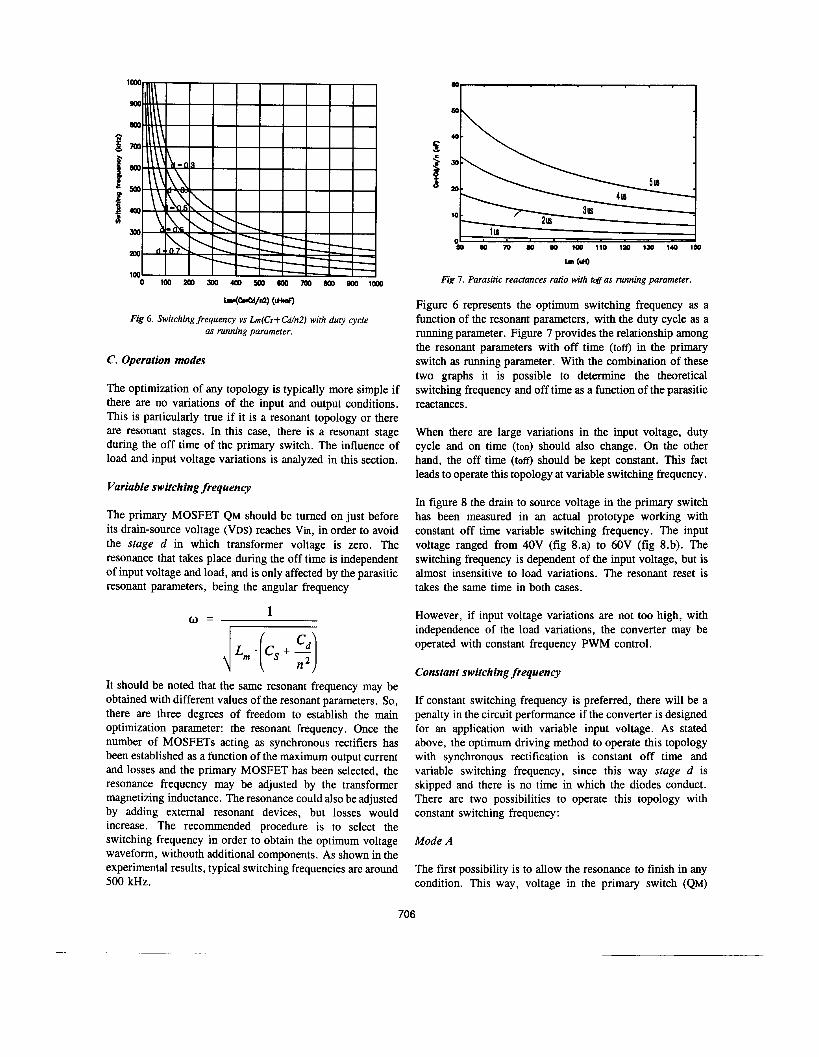
wcrcd/nl) (rHnF)
Fig 6 . Switchingfrequency vs Ln(Cs+Gi/n2) with duty cycle as running parameter.
C. Operation modes
The optimization of any topology is typically more simple if there are no variations of the input and output conditions. This is particularly true if it is a resonant topology or there are resonant stages. In this case, there is a resonant stage during the off time of the primary switch. The influence of load and input voltage variations is analyzed in this section.
Variable switching frequency
The primary MOSFET QM should be turned on just before its drain-source voltage (VDS) reaches Vin, in order to avoid the stage d in which transformer voltage is zero. The resonance that takes place during the off time is independent of input voltage and load, and is only affected by the parasitic resonant parameters, being the angular frequency
1 o =
It should be noted that the same resonant frequency may be obtained with different values of the resonant parameters. So, there are three degrees of freedom to establish the main optimization parameter: the resonant frequency. Once the number of MOSFETs acting as synchronous rectifiers has been established as a function of the maximum output current and losses and the primary MOSFET has been selected, the resonance frequency may be adjusted by the transformer magnetizing inductance. The resonance could also be adjusted by adding external resonant devices, but losses would increase. The recommended procedure is to select the switching frequency in order to obtain the optimum voltage waveform, withouth additional components. As shown in the experimental results, typical switching frequencies are around 500 kHz.
IJn (4
Fig 7. Parasitic reactances ratio with t@ as running parameter.
Figure 6 represents the optimum switching frequency as a function of the resonant parameters, with the duty cycle as a running parameter. Figure 7 provides the relationship among the resonant parameters with off time (toff) in the primary switch as running parameter. With the combination of these two graphs it is possible to determine the theoretical switching frequency and off time as a function of the parasitic reactances.
When there are large variations in the input voltage, duty cycle and on time (ton) should also change. On the other hand, the off time (toff) should be kept constant. This fact leads to operate this topology at variable switching frequency.
In figure 8 the drain to source voltage in the primary switch has been measured in an actual prototype working with constant off time variable switching frequency. The input voltage ranged from 40V (fig 8.a) to 6OV (fig 8.b). The switching frequency is dependent of the input voltage, but is almost insensitive to load variations. The resonant reset is takes the same time in both cases.
However, if input voltage variations are not too high, with independence of the load variations, the converter may be operated with constant frequency PWM control.
Constant switching frequency
If constant switching frequency is preferred, there will be a penalty in the circuit performance if the converter is designed for an application with variable input voltage. As stated above, the optimum driving method to operate this topology with synchronous rectification is constant off time and variable switching frequency, since this way stage d is skipped and there is no time in which the diodes conduct. There are two possibilities to operate this topology with constant switching frequency:
Mode A
The first possibility is to allow the resonance to finish in any condition. This way, voltage in the primary switch (QM)
706
* . . .
1
Fig 8. VDS (SOV/div, 500 ns/div) at Vin=40V (a) and Vin=6OV (b) for Io=15A.
before the turn on is always the input voltage. Turn on losses will be dependent of the input voltage but independent of the duty cycle. The problem, however, is that stage d exists, and diodes conduct. It is necessary to connect a Schottky diode in parallel with SR2.
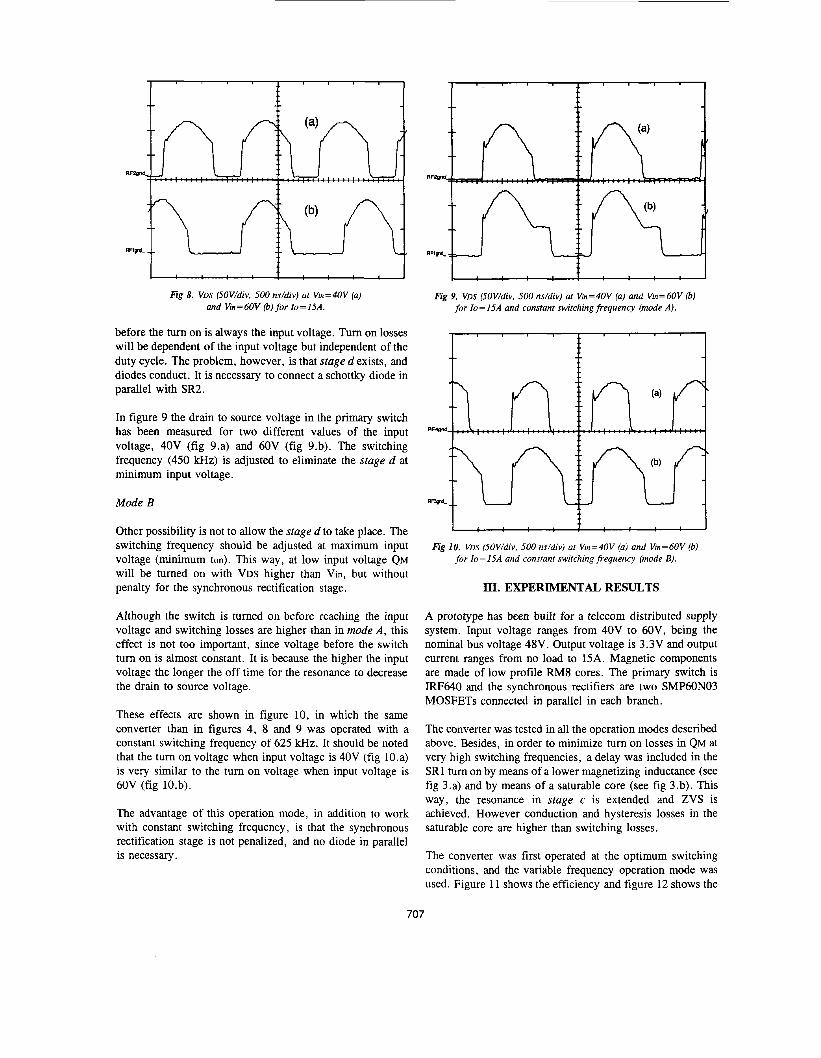
In figure 9 the drain to source voltage in the primary switch has been measured for two different values of the input voltage, 40V (fig 9.a) and 60V (fig 9.b). The switching frequency (450 kHz) is adjusted to eliminate the stage d at minimum input voltage.
Mode B
Other possibility is not to allow the stage d to take place. The switching frequency should be adjusted at maximum input voltage (minimum ton). This way, at low input voltage QM will be turned on with VDS higher than Vin, but without penalty for the synchronous rectification stage.
Although the switch is turned on before reaching the input voltage and switching losses are higher than in mode A , this effect is not too important, since voltage before the switch turn on is almost constant. It is because the higher the input voltage the longer the off time for the resonance to decrease the drain to source voltage.
These effects are shown in figure 10, in which the same converter than in figures 4, 8 and 9 was operated with a constant switching frequency of 625 kHz. It should be noted that the turn on voltage when input voltage is 40V (fig 10.a) is very similar to the turn on voltage when input voltage is 60V (fig 10.b).
The advantage of this operation mode, in addition to work with constant switching frequency, is that the synchronous rectification stage is not penalized, and no diode in parallel is necessary.
I I I ! I
Fig 9. VDS (SOV/div, 500 ns/div) at Vin=40V (a) and Vin=bOV (b) for Io=15A and constant switching frequency (mode A).
I ! ! ! ! ? ! 1
Fig 10. VDS (SOV/div, 500 ns/div) at Vin=40V (a) and Vin=6OV (b) for Io = 15A and constant switching frequency (mode B).
111. EXPERIMENTAL RESULTS
A prototype has been built for a telecom distributed supply system. Input voltage ranges from 40V to 60V, being the nominal bus voltage 48V. Output voltage is 3.3V and output current ranges from no load to 15A. Magnetic components are made of low profile RM8 cores. The primary switch is IRF640 and the synchronous rectifiers are two SMP60N03 MOSFETs connected in parallel in each branch.
The converter was tested in all the operation modes described above. Besides, in order to minimize turn on losses in QM at very high switching frequencies, a delay was included in the SR1 turn on by means of a lower magnetizing inductance (see fig 3.a) and by means of a saturable core (see fig 3.b). This way, the resonance in stage c is extended and ZVS is achieved. However conduction and hysteresis losses in the saturable core are higher than switching losses.
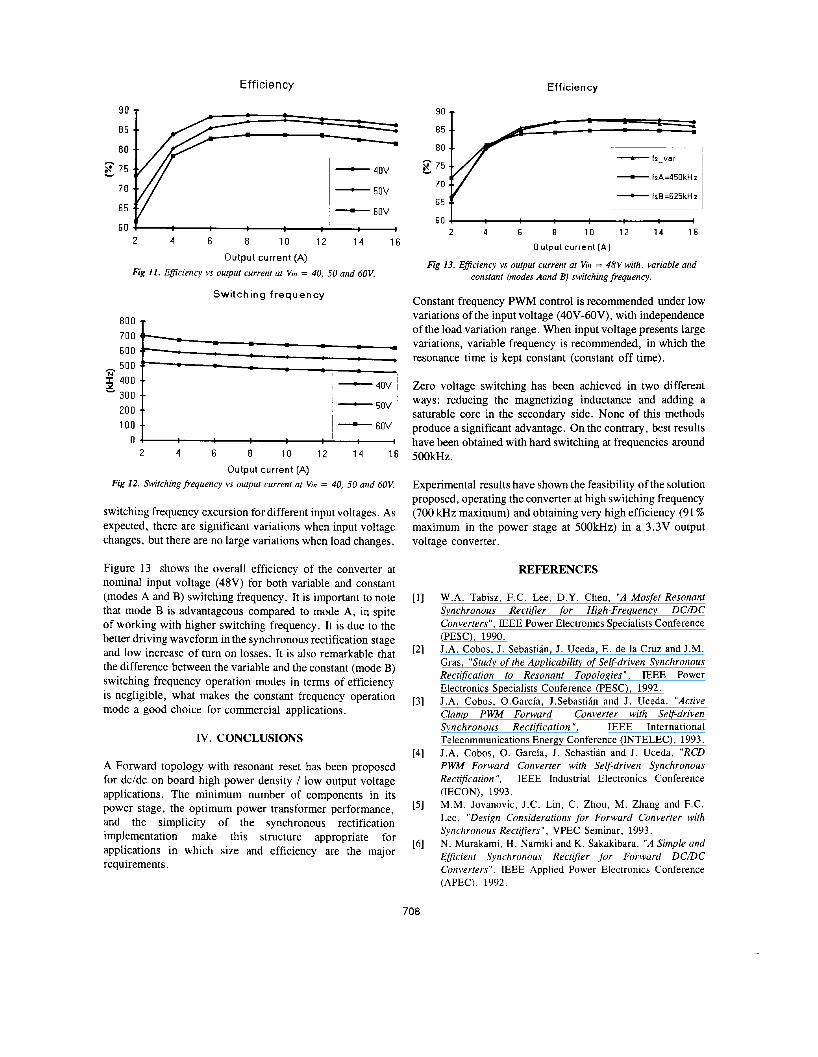
The converter was first operated at the optimum switching conditions, and the variable frequency operation mode was used. Figure 11 shows the efficiency and figure 12 shows the
707
Efficiency Efficiency
90
8 5
80
7 5
7 0
6 5 f/ I - 60V ~. - 6 0 1 I
2 4 6 8 1 0 1 2 1 4 1 6 Output current (A)
Fig 11. Eficiency vs output current at Kn = 40, 50 and 60V.
Switch ing f r e q u e n c y
8 0 0 T
2 1 : : : : : ;-50vr
100 1 - 60V 1
2 4 6 8 1 0 1 2 1 4 1 6 Output current (A)
0
Fig 12. Switching frequency vs output current at K n = 40, 50 and 60V.
switching frequency excursion for different input voltages. As expected, there are significant variations when input voltage changes, but there are no large variations when load changes.
Figure 13 shows the overall efficiency of the converter at nominal input voltage (48V) for both variable and constant (modes A and B) switching frequency. It is important to note that mode B is advantageous compared to mode A, in spite of working with higher switching frequency. It is due to the better driving waveform in the synchronous rectification stage and low increase of turn on losses. It is also remarkable that the difference between the variable and the constant (mode B) switching frequency operation modes in terms of efficiency is negligible, what makes the constant frequency operation mode a good choice for commercial applications.
IV. CONCLUSIONS
A Forward topology with resonant reset has been proposed for dcldc on board high power density I low output voltage applications. The minimum number of components in its power stage, the optimum power transformer performance, and the simplicity of the synchronous rectification implementation make this structure appropriate for applications in which size and efficiency are the major requirements.
90
85
80 r--- ' - fs-var g 75 - fsA=450kHz - fsB =625kH z 70
65
60
~~~ -
2 4 6 8 10 1 2 1 4 16
Output current [ A ]
Fig 13. Eficiency vs output current at Kn = 48V with. variable and constant (modes Aand B) switching frequency.
Constant frequency PWM control is recommended under low variations of the input voltage (40V-60V), with independence of the load variation range. When input voltage presents large variations, variable frequency is recommended, in which the resonance time is kept constant (constant off time).
Zero voltage switching has been achieved in two different ways: reducing the magnetizing inductance and adding a saturable core in the secondary side. None of this methods produce a significant advantage. On the contrary, best results have been obtained with hard switching at frequencies around SOOkHz.
Experimental results have shown the feasibility of the solution proposed, operating the converter at high switching frequency (700 kHz maximum) and obtaining very high efficiency (91 % maximum in the power stage at SOOkHz) in a 3.3V output voltage converter.
REFERENCES
W.A. Tabisz, F.C. Lee, D.Y. Chen, " A Mosfet Resonant Synchronous Rectijier f o r High-Frequency DC/DC Converters", IEEE Power Electronics Specialists Conference (PESC), 1990. J.A. Cobos, J. Sebastian, J. Uceda, E. de la Cruz and J.M. Gras, "Study of the Applicability of Self-driven Synchronous Rectijication to Resonant Topologies", IEEE Power Electronics Specialists Conference (PESC), 1992. J.A. Cobos, O.Garcia, J.Sebastiin and J . Uceda. "Active Clamp PWM Forward Converter with Self-driven Synchronous Rectification ' I , IEEE International Telecommunications Energy Conference (INTELEC), 1993. J.A. Cobos, 0. Garcia, J. Sebastian and J. Uceda, "RCD PWM Forward Converter with Self-driven Synchronous Rectification 'I, IEEE Industrial Electronics Conference (IECON), 1993. M.M. Jovanovic, J.C. Lin, C. Zhou, M. Zhang and F.C. Lee, "Design Considerations fo r Forward Converter with Synchronous Rectijiers" , VPEC Seminar, 1993. N. Murakami, H. Namiki and K. Sakakibara. " A Simple and Eficient Synchronous Rectijier for Forward DCIDC Converters", IEEE Applied Power Electronics Conference (APEC), 1992.
708


