Embed Size (px)
Citation preview
Self-assembled conjugated polymer–surfactant–silica mesostructures andtheir integration into light-emitting diodes{
E. Dovgolevsky,a S. Kirmayer,a E. Lakin,a Y. Yang,b C. J. Brinkerb and G. L. Frey*a
Received 28th August 2007, Accepted 12th November 2007
First published as an Advance Article on the web 29th November 2007
DOI: 10.1039/b713170d
A self-assembly process for the preparation of functional mesoscopically ordered semiconducting
polymer–silica nanocomposite thin films is reported. The nanocomposites are prepared by
introducing pre-synthesized semiconducting polymers into a tetrahydrofuran (THF)–water
homogeneous sol solution containing silica precursor species and a surface-active agent.
Depending on the concentration of the surface-active agent, it was possible to prepare materials
with three different types of mesostructural order: i) a 2D hexagonal mesophase silica with
conjugated polymer guest species incorporated within the hydrophobic cylinders organized in
domains aligned parallel to the substrate surface plane; ii) a lamellar mesophase silica with the
layers oriented parallel to the substrate surface and the conjugated polymer guest species
incorporated in the hydrophobic layers; or iii) an apparent intermediate phase consisting of a
mixture of the hexagonal and lamellar phases in addition to worm-like aggregates with no
appreciable orientational order. The continuous through-film conductive pathway provided by
the intermediate phase has allowed the integration of ordered semiconducting polymer–silica
nanocomposites into opto-electronic devices. By comparison, the lamellar mesostructure prevents
through-film conduction, with the result that no light emission occurs. Blue-, green- and
red-emitting diodes comprising blue-emitting poly(9,9-dioctylfluorenyl-2,7-diyl) (PFO),
green-emitting poly(9,9-dioctylfluorenyl-2,7-diyl)-co-1,4-benzo-(2,19,3)-thiadiazole) (F8BT), and
red-emitting poly[2-methoxy-5(29-ethyl-hexyloxy)-1,4-phenylenevinylene] (MEHPPV) confined
within the 2D hexagonal silica nanostructure were fabricated with luminances of ca. 3 cd m22 at
15 V. Device performances provide criteria for optimizing the selection of synthesis chemistries,
processing conditions, compositions, and structures, for light-emission properties sought.
Introduction
Conjugated polymers have been the subject of extensive
academic and industrial research efforts due to their promising
potentials for use as active layers in electronic and opto-
electronic devices, such as light-emitting diodes,1,2 field-effect
transistors (FETs),3,4 lasers,5 photodiodes6 and solar cells.7,8 In
these various applications it has been found that, in addition to
the intrinsic chemical properties of the polymers and additives,
the device performance is strongly dependent on the morpho-
logy of the film in which the polymer is cast, which can be
influenced further by incorporation into a suitable host matrix.
Therefore, attaining control over the chemical composition,
morphology and hierarchical structure in the polymer or
composite film is expected to enhance device performance and
enable the design and fabrication of new types of devices.
The influence of film morphology and interfacial inter-
actions on the mechanical properties of many composite
materials based on conventional polymers are well-known.9
Composite materials are generally designed to enhance or
exhibit properties and functions that are unattainable from the
individual chemical species or their phases. Polymer–inorganic
composites harness the good processability and low density of
the polymer component, in combination with the high
strength, stiffness, thermal stability, and mechanical durability
of the inorganic component. Consequently, synthetic appro-
aches have been developed to control the polymer–inorganic
solution and processing chemistries, their physicochemical
interactions, and their hierarchical architectures at molecular
and mesoscale levels towards specific applications.10–12
In this study, polymer–inorganic guest–host composite
materials are designed, synthesized, characterized, and inte-
grated into opto-electronic devices. The device performances
confirm the successful design and synthesis of the nano-
composites and yield deep insight into the molecular and
electronic processes of the materials. Such understanding
provides important feedback for optimizing the synthesis
chemistry and properties of novel functional conjugated
polymer–inorganic nanocomposite materials.
Depending upon the nature of the association between the
inorganic and polymeric components, nanocomposites can be
classified into two categories: one in which the inorganic
material (e.g., nanoparticles, colloids, polyoxometalates) is
embedded in a polymeric matrix,13 and a second, where
aDepartment of Materials Engineering, Technion – Israel Institute ofTechnology, Haifa 32000, IsraelbDepartment of Chemical and Nuclear Engineering, University of NewMexico and Sandia National Laboratory/UNM Advanced MaterialsLab, Albuquerque, NM 87106, USA{ Electronic supplementary information (ESI) available: The absorp-tion spectra of PFO-incorporated Brij-56–silica, and PFO–PEO–silicafilms, compared to those of pristine PFO polymer films prepared bydip-coating and casting. See DOI: 10.1039/b713170d
PAPER www.rsc.org/materials | Journal of Materials Chemistry
This journal is � The Royal Society of Chemistry 2008 J. Mater. Chem., 2008, 18, 423–436 | 423
organic polymers are confined within an inorganic template.14
Incorporation of polymers into well-defined channels of an
insulating mesoporous inorganic scaffold offers control over
the conformation of individual polymer chains, chain–chain
stacking, and interfacial interactions with the scaffold ‘‘walls’’,
while providing environmental isolation. Furthermore, highly
ordered (nano)engineered voids of an inorganic matrix can be
used to induce alignment and preferred orientational ordering
of the polymer chains.
Organic-in-inorganic composites present several advantages
as optical materials including: mild synthesis conditions,
simple processability, mechanical robustness, and most impor-
tantly, the ability to tailor the optical properties through host–
guest material selection and control of organic–inorganic
interactions on a molecular level. Optically responsive dye-
incorporated-silica-based hybrid materials have been suggested
for fundamental studies such as the spectroscopy of isolated
dye molecules in a sol–gel matrix, energy transfer in solids, and
the following of the sol–gel process in situ via luminescent
probes.15–19 Furthermore, materials with organic dye species
included in mesostructured inorganic host matrices, such as
silica or zirconia, have shown improved combinations of
optical, mechanical, and thermal properties for photochromic,
optical limiting, sensor, and laser applications.15,20,21
Electronic and opto-electronic applications, however,
require that a continuous conductive pathway through the
material be present to support charge transport. Boilot and
co-workers reported the use of organic–inorganic composites
prepared from silane precursors modified with hole- or
electron-transporting units and light-emitting species.22 In this
system, the chromophores were covalently bound to the
amorphous conductive inorganic framework. A film of this
hybrid material sandwiched between indium–tin oxide (ITO)
and a cathode produced electroluminescence under forward
bias. This light-emitting diode (LED) device exploited sol–gel
chemistry for the synthesis of an amorphous organic–inorganic
hybrid material, but without self-organization into ordered
mesostructures.
The use of orientationally ordered mesostructured materials
for controlling the optical and electrical properties of
semiconducting polymers was first demonstrated for a con-
jugated polymer–mesoporous nanocomposite.23–25 In these
studies, a semiconducting polymer, poly[2-methoxy-5(29-ethyl-
hexyloxy)-1,4-phenylenevinylene] (MEH-PPV), was infiltrated
into the channels of a pre-formed hexagonal mesoporous
silica-host. The architecture of the material allowed the authors
to quantify the roles of interchain and intrachain energy
transfer in conjugated polymers.24 Infiltration of polythio-
phene into a mesoporous titania scaffold for the preparation of
photovoltaic devices has also been attempted.26 Polymer
infiltration, however, can be difficult to control because it
depends on both partitioning of the polymer from the solvent
and reptation into the pore channels, which can be slow due to
diffusion limitations. A distribution of polymer chain environ-
ments may therefore exist depending on whether the con-
jugated polymer guest species are fully incorporated, partially
incorporated or not incorporated (estimated to be y20%) in
the mesoporous inorganic host.23–25 For such heterogeneous
distributions, accompanying broad distributions of electronic
and optical properties may result that are also challenging to
control and optimize. Furthermore, the reptation of polymer
chains through the entire micron-thick porous films necessary
for device operation, if possible, may require long processing
times and elevated temperatures.23
In another approach, semiconducting polymers were
fully incorporated into a silica scaffold by in situ polymeriza-
tion.27–30 Although the insertion of reactive monomers into
the silica scaffold is relatively simple, in situ polymerization
often results in high contamination levels of unreacted
precursor monomers and leaving groups due to modest extents
of polymerization and sluggish molecular diffusion from the
inorganic mesopores, respectively. Low-polymerization yields
tend to result in the presence of non-conductive segments in
the polymer chains that impede or altogether suppress carrier
transport in the corresponding devices.
An alternative approach is to incorporate high-molecular-
weight conjugated polymer species during synthesis and
processing of the self-assembling inorganic–surfactant meso-
structured host. One way to do so is to prepare thin films of
mesostructured silica by evaporation-induced self-assembly
(EISA). In this process, thin films are deposited from an
EtOH–water solution containing silica precursor and surfac-
tant species initially below the critical micelle concentration
(cmc) of the solution.31,32 Preferential evaporation of ethanol
during dip-coating concentrates the non-volatile surfactant
and silica species, which under the right conditions will
co-assemble. Progressively increasing concentrations tend to
promote the formation of highly ordered silica–surfactant
mesophases, which are fixed by silica polymerization. The
EISA process provides a simple coating procedure and is
advantageous for the deposition of conjugated polymer–silica
nanocomposite films in view of their integration into opto-
electronic applications.
Semiconducting polymers, however, are not soluble in polar
solvents and therefore not amenable for introduction into
sol–gel precursor solutions. As a consequence, one must select
a solvent that is compatible with both cross-linkable inorganic
precursor species and the functional semiconducting polymer
guests to circumvent undesirable macrophase separation.
Moreover, because solid-state effects greatly influence the
optical and electrical properties of conjugated polymers, the
selected solvent must be sufficient to avoid aggregation and
p–p stacking of the semiconducting polymer, which restricts
substantially the options available. Water-soluble dye mole-
cules are abundant, and therefore, preparation of optically-
responsive dye-incorporated mesostructured silica does
not suffer solubility limitations. Opto-electronic properties,
however, require also a continuous conductive pathway
for carrier mobility. Whereas through-film conductivity is
generally unattainable in unstructured dye–silica blends,
conjugated polymers incorporated in mesostructured silica
matrices can yield robust opto-electronic properties, depending
on the connectivity and alignment of the mesochannels.
An important consideration for the selected solvent is that it
must solublize both the hydrophobic semiconducting polymer
and the silica precursor species. A useful means for estimating
the solubility of a polymer in a solvent is the squared difference
of the Hildebrand parameters of the solvent and solute
424 | J. Mater. Chem., 2008, 18, 423–436 This journal is � The Royal Society of Chemistry 2008
(dsolvent 2 dsolute)2. Similar d values for the solvent and polymer
solute indicate good mutual solubility. For example, poly-
fluorene has a d value of approximately 9.1 to 9.3 (cal cm23)1/2,
compared to THF (dTHF= 9.1) and chloroform (dCHCl3= 9.1),
which are known to be good solvents for polyfluorene; toluene
(dTol= 8.9) and chlorobenzene (dCB= 9.5) are moderately good
solvents; while cyclohexane (dCH= 8.2) and dichloroethane
(dDCE= 9.8) are moderately poor and very poor, respectively.33
In addition to the Hildebrand solubility parameter, it is
important to also consider the polymer–solvent interactions.
For example, the d value of MEH-PPV is similar to that of
THF and chlorobenzene, however, MEH-PPV chains tend to
form tight coils with short conjugation lengths and restricted
aggregation in non-aromatic organic solvents, such as THF,
while maintaining an open and straight conformation with a
longer mean conjugation length that promotes aggregation in
aromatic chlorobenzene solutions.34 These polymer aggregates
may reside in the film during the slow evaporation of relatively
high boiling-point solvents, like chlorobenzene, and result in
macroscopically phase-separated domains of the conjugated
polymer in the silica matrix.34,35 Rapid evaporation of a
volatile solvent, such as THF, on the other hand, avoids
segregation of the semiconducting polymer, though must be
balanced to permit self-assembly of the structure-directing
species. High solvent volatility and accompanying low visco-
sity is also essential for the deposition of thin films using the
EISA method.36 Accordingly, the preparation of transparent
mesostructured organosilica in host polymer membranes by
in situ growth in THF solution was very recently reported,
although no optical guest species were incorporated.37
Here, we describe a robust new synthetic approach for
the preparation of mesoscopically ordered semiconducting
polymer–silica nanocomposite thin films through the co-
assembly of silica precursor species, surfactant, and pre-
polymerized semiconducting polymers from a homogeneous
THF–water solution. In this process, the commercially
available hydrophobic semiconducting polymers are, for the
first time, incorporated into the mesostructured silica upon its
formation. The optical and electrical properties of the
conjugated polymers are maintained upon incorporation,
enabling their utilization in opto-electronic applications. A
non-ionic surfactant, Brij-56, was used in this study because it
is known to direct the deposition of a variety of phases in the
conventional sol–gel process, and will not contribute parasitic
ionic currents to devices comprising the mesostructured
films.38,39 However, the approach reported here is general
and can be easily implemented to a variety of different non-
ionic surfactants, inorganic host matrices and conjugated
polymers. Encapsulation of the conjugated polymer species in
the mesostructured host could also offer improved mechanical
and environmental stability against external chemical and
mechanical damage.40–42
Experimental
Materials
Tetraethylorthosilicate (TEOS), hydrochloric acid (HCl) and
tetrahydrofuran (THF) (Aldrich) were used as the silica
precursor, catalyst and solvent, respectively. An amphiphilic
non-ionic polymer, Brij-56TM
poly(oxyethylene) cetylether
(CH3(CH2)15–(OCH2CH2)10–OH)) (Aldrich) was used as
structure-directing agent. Three semiconducting polymers
(American Dye Source) were used: poly((9,9-dioctylfluorenyl-
2,7-diyl)) (PFO, Mw = 80 000), poly((9,9-dioctylfluorenyl-2,7-
diyl)-co-1,4-benzo-(2,19,3)-thiadiazole) (F8BT, Mw = 15 000),
and poly(2-methoxy-5-(2-ethyl hexyloxy)-1,4-phenylenevinyl-
ene (MEH-PPV, Mw = 480 000).
Synthesis of silica sol
In a typical synthesis, a THF-rich–water sol solution was
prepared from TEOS, Brij-56, HCl catalyst and a semi-
conducting polymer, either PFO, F8BT or MEH-PPV. First,
15 ml of TEOS were prehydrolyzed in a solution containing
6 ml of 0.07 N HCl and 75 ml of THF and stirred vigorously at
room temperature for 1 h. Then, to 1.5 ml of this solution,
either 0.237, 0.178 or 0.089 g of Brij-56 surfactant were added
so that the surfactant concentration (c0) in the sol solution is 8,
6, or 3 wt%, respectively. Finally, 1.5 ml of this sol solution
was then mixed with 2.25 ml of a THF filtered solution
containing either 5.6 mg MEH-PPV or F8BT, or 3.4 mg PFO.
The lower PFO concentration is due to its lower solubility in
the sol solution compared to that of F8BT and MEH-PPV.
For example, the final mole ratios in the semiconducting
polymer–6 wt%-Brij56–silica sol solution prior to dip-coating
are: 1 TEOS : 40.27 THF : 4.96 H2O : 6.3 6 1023 HCl : 4.13 61025 PFO or 3.57 6 1024 F8BT or 1.11 6 1025 MEH-PPV :
0.249 Brij-56, respectively. The semiconducting polymer–
Brij-56 molar ratio was kept constant in all precursor
solutions. For example, the semiconducting polymer–3
wt%-Brij-56–silica sol solution was prepared following the
procedure detailed above for the semiconducting polymer–6
wt%-Brij-56–silica sol solution, adding the same volume
of THF with only half of the semiconducting polymer
concentration.
Thin film preparation
Nanocomposite thin films were prepared by dip-coating at a
rate of 20 ipm, spin-coating at 1500–2000 rpm, or drop-casting
in ambient atmosphere (23–25 uC, and 75–85% of relative
humidity) on ,100. single-crystal Si wafers, glass slides,
polyimide films or ITO substrates. All deposited thin films
were continuous, uniform and crack-free as evident from high-
resolution scanning electron microscopy.
Conjugated polymer loadings of the nanocomposite films
were estimated by dissolving the product films in small
amounts of THF under vigorous stirring. The concentration
of the polymer in the solution was determined by optical
absorption spectroscopy, and the substrate weighed prior to
and after film removal, from which conjugated polymer
concentrations in the films was estimated.
Characterization
X-Ray diffraction (XRD) measurements were performed on
a Bede D3 X-ray diffractometer equipped with an 18 kW
Rigaku rotating anode generator at h–2h scan mode in reflec-
tion geometry. A highly monochromatized CuKa1 line with
This journal is � The Royal Society of Chemistry 2008 J. Mater. Chem., 2008, 18, 423–436 | 425
l = 1.5406 A was selected from the primary X-ray beam by
means of two channel-cut (220) Si crystals. Small-angle X-ray
scattering measurements (SAXS) were performed using a
small-angle diffractometer (Bruker Nanostar, KFF CU 2
K-90) with CuKa radiation with l = 1.542 A. Pinhole
collimation yielding a beam 100 mm in diameter and a
10 6 10 cm2 two-dimensional position-sensitive wire detector
positioned 65 cm behind the sample were used. The patterns
were recorded using an acceleration voltage of 40 kV and
acceleration current of 30 mA. The polyimide substrates were
vertically located in the SAXS diffractometer and patterns
were recorded in transmission mode with fixed incidence angle
a (the angle between the incident beam and the sample surface)
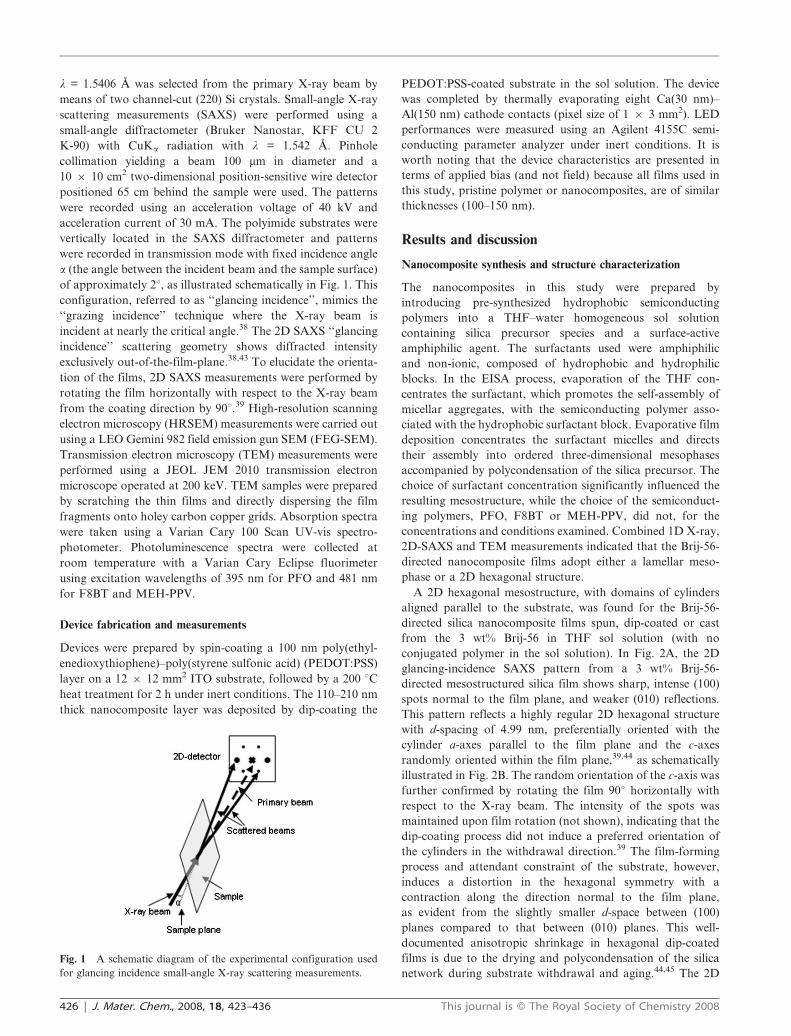
of approximately 2u, as illustrated schematically in Fig. 1. This
configuration, referred to as ‘‘glancing incidence’’, mimics the
‘‘grazing incidence’’ technique where the X-ray beam is
incident at nearly the critical angle.38 The 2D SAXS ‘‘glancing
incidence’’ scattering geometry shows diffracted intensity
exclusively out-of-the-film-plane.38,43 To elucidate the orienta-
tion of the films, 2D SAXS measurements were performed by
rotating the film horizontally with respect to the X-ray beam
from the coating direction by 90u.39 High-resolution scanning
electron microscopy (HRSEM) measurements were carried out
using a LEO Gemini 982 field emission gun SEM (FEG-SEM).
Transmission electron microscopy (TEM) measurements were
performed using a JEOL JEM 2010 transmission electron
microscope operated at 200 keV. TEM samples were prepared
by scratching the thin films and directly dispersing the film
fragments onto holey carbon copper grids. Absorption spectra
were taken using a Varian Cary 100 Scan UV-vis spectro-
photometer. Photoluminescence spectra were collected at
room temperature with a Varian Cary Eclipse fluorimeter
using excitation wavelengths of 395 nm for PFO and 481 nm
for F8BT and MEH-PPV.
Device fabrication and measurements
Devices were prepared by spin-coating a 100 nm poly(ethyl-
enedioxythiophene)–poly(styrene sulfonic acid) (PEDOT:PSS)
layer on a 12 6 12 mm2 ITO substrate, followed by a 200 uCheat treatment for 2 h under inert conditions. The 110–210 nm
thick nanocomposite layer was deposited by dip-coating the
PEDOT:PSS-coated substrate in the sol solution. The device
was completed by thermally evaporating eight Ca(30 nm)–
Al(150 nm) cathode contacts (pixel size of 1 6 3 mm2). LED
performances were measured using an Agilent 4155C semi-
conducting parameter analyzer under inert conditions. It is
worth noting that the device characteristics are presented in
terms of applied bias (and not field) because all films used in
this study, pristine polymer or nanocomposites, are of similar
thicknesses (100–150 nm).
Results and discussion
Nanocomposite synthesis and structure characterization
The nanocomposites in this study were prepared by
introducing pre-synthesized hydrophobic semiconducting
polymers into a THF–water homogeneous sol solution
containing silica precursor species and a surface-active
amphiphilic agent. The surfactants used were amphiphilic
and non-ionic, composed of hydrophobic and hydrophilic
blocks. In the EISA process, evaporation of the THF con-
centrates the surfactant, which promotes the self-assembly of
micellar aggregates, with the semiconducting polymer asso-
ciated with the hydrophobic surfactant block. Evaporative film
deposition concentrates the surfactant micelles and directs
their assembly into ordered three-dimensional mesophases
accompanied by polycondensation of the silica precursor. The
choice of surfactant concentration significantly influenced the
resulting mesostructure, while the choice of the semiconduct-
ing polymers, PFO, F8BT or MEH-PPV, did not, for the
concentrations and conditions examined. Combined 1D X-ray,
2D-SAXS and TEM measurements indicated that the Brij-56-
directed nanocomposite films adopt either a lamellar meso-
phase or a 2D hexagonal structure.
A 2D hexagonal mesostructure, with domains of cylinders
aligned parallel to the substrate, was found for the Brij-56-
directed silica nanocomposite films spun, dip-coated or cast
from the 3 wt% Brij-56 in THF sol solution (with no
conjugated polymer in the sol solution). In Fig. 2A, the 2D
glancing-incidence SAXS pattern from a 3 wt% Brij-56-
directed mesostructured silica film shows sharp, intense (100)
spots normal to the film plane, and weaker (010) reflections.
This pattern reflects a highly regular 2D hexagonal structure
with d-spacing of 4.99 nm, preferentially oriented with the
cylinder a-axes parallel to the film plane and the c-axes
randomly oriented within the film plane,39,44 as schematically
illustrated in Fig. 2B. The random orientation of the c-axis was
further confirmed by rotating the film 90u horizontally with
respect to the X-ray beam. The intensity of the spots was
maintained upon film rotation (not shown), indicating that the
dip-coating process did not induce a preferred orientation of
the cylinders in the withdrawal direction.39 The film-forming
process and attendant constraint of the substrate, however,
induces a distortion in the hexagonal symmetry with a
contraction along the direction normal to the film plane,
as evident from the slightly smaller d-space between (100)
planes compared to that between (010) planes. This well-
documented anisotropic shrinkage in hexagonal dip-coated
films is due to the drying and polycondensation of the silica
network during substrate withdrawal and aging.44,45 The 2D
Fig. 1 A schematic diagram of the experimental configuration used
for glancing incidence small-angle X-ray scattering measurements.
426 | J. Mater. Chem., 2008, 18, 423–436 This journal is � The Royal Society of Chemistry 2008
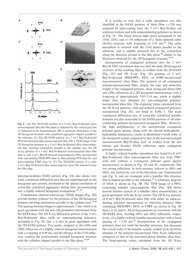
glancing-incidence SAXS pattern (Fig. 2A) also shows very
weak continuous diffraction arcs that are superimposed on the
hexagonal spot pattern, attributed to the spatial correlation of
worm-like cylindrical aggregates during their pre-positioning
into a highly ordered hexagonal arrangement.46–48
Transmission electron microscopy (TEM) images (Fig. 2D)
provide further evidence for the presence of the 2D hexagonal
domains showing orientations parallel to the cylinder axes.39,44
The spacing between fringes is approximately 5 nm, which is in
good agreement with the unit cell parameters determined from
the SAXS data. The 1D X-ray diffraction pattern of the 3 wt%
Brij-56-directed silica (with no semiconducting polymer),
presented in Fig. 2E, line i, is also in good agreement with
the 2D-SAXS pattern. Two peaks, assigned to the (100) and
(200) reflections of a highly ordered hexagonal mesostructure
with a d-spacing of 4.99 nm, and the absence of the (110) reflec-
tion, confirm the preferentially oriented hexagonal structure
with the cylinders aligned parallel to the film plane.39,44
It is worthy to note that a cubic mesophase was also
identified in the SAXS patterns of thick films (y230 nm)
prepared by spin-coating from the 3 wt% Brij-56-silica sol
solutions without and with semiconducting polymers as shown
in Fig. 2F. The sharp intense eight spots correspond to the
(110), (101), and (1–10) reflections of a body-centered cubic
(Im3m) structure with d-spacing of 5.45 nm.49 The cubic
mesophase is oriented with the (110) planes parallel to the
substrate, and is slightly distorted due to the contraction
along the direction normal to the film plane,49 similar to the
distortion observed for the 2D hexagonal structure.44,45
Incorporation of conjugated polymers into the 3 wt%
Brij-56 THF sol solution does not alter the main 2D-hexagonal
structure of the resulting films, as evident from the 2D-SAXS
(Fig. 2C) and 1D X-ray (Fig. 2E) patterns of 3 wt%
Brij-56-directed MEH-PPV, PFO, or F8BT-incorporated
mesostructured silica films. The patterns of all conjugated
polymer-incorporated films, despite the type and molecular
weight of the conjugated polymer, show strong and sharp (100)
and (200) reflections of a 2D hexagonal mesostructure with a
d-spacing of approximately 5.05–5.14 nm, which is slightly
larger than that obtained for non-conjugated polymer-
incorporated silica film. The d-spacing values calculated from
the 1D X-ray patterns, with and without conjugated polymers
incorporated (Fig. 2E), are listed in Table 1. The weak
continuous diffraction arcs of worm-like cylindrical micelles
domains are also noticeable in the SAXS patterns of all semi-
conducting polymer-incorporated hexagonal films. However,
the high polydispersity of the incorporated conjugated
polymer guest species, along with the altered hydrophobic–
hydrophilic interactions, results in diminished overall order of
the hexagonal system compared to that of the non-intercalated
mesostructured Brij-56-silica host as evident from the less
intense and broader SAXS reflections upon conjugated
polymer incorporation.
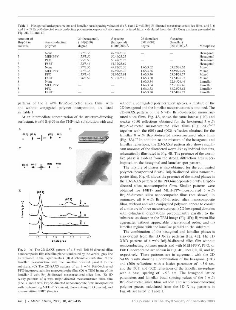
A highly ordered lamellar mesophase was found for 8 wt%
Brij-56-directed silica nanocomposite films cast from THF,
with and without a conjugated polymer guest species
incorporated, as shown in Fig. 3A and 3C, respectively. The
two strong reflections, in both patterns, indexed as (001) and
(002), are exclusively out-of-the-film-plane (see Experimental
and Fig. 1), and are consistent with a lamellar film structure
that is aligned parallel to the substrate,44 a schematic diagram
of which is shown in Fig. 3B. The TEM image of a PFO-
containing lamellar nanocomposite film (Fig. 3D) shows
layered features typical of a lamellar silica mesostructure, in
good agreement with the X-ray results. The 1D X-ray patterns
of 8 wt% Brij-56-directed silica film with either no semicon-
ducting polymers incorporated or otherwise identical films
containing MEH-PPV, PFO, or F8BT are shown in Fig. 3E
lines i, ii, iii, and iv. All of these patterns are consistent with the
2D-SAXS data, showing (001) and (002) reflections, respec-
tively, of a highly ordered lamellar mesostructure with a basal
spacing of y5.30 nm.44 Incorporation of the conjugated
polymers does not swell the lamellar structure, but decreases
the overall order of the lamellar system, evident from the lower
intensity of the polymer-incorporated films X-ray reflections
compared to that of the non-intercalated lamellar silica host.
The basal-spacing values calculated from the 1D X-ray
Fig. 2 (A) The 2D-SAXS pattern of a 3 wt% Brij-56-directed silica
nanocomposite film (the film plane is indicated by the vertical grey line
as explained in the Experimental), (B) A schematic illustration of the
2D hexagonal domains with cylindrical aggregates aligned parallel to
the substrate. (C) The 2D SAXS pattern of a 3 wt% Brij-56-directed
PFO-incorporated silica nanocomposite film. (D) A TEM image of the
2D hexagonal domains in a 3 wt% Brij-56-directed silica nanocompo-
site film, showing orientations parallel to the cylinder axis. (E) 1D
X-ray patterns of a 3 wt% Brij-56-directed mesostructured silica film
(line i), and 3 wt% Brij-56-directed nanocomposite films incorporated
with: red-emitting MEH-PPV (line ii), blue-emitting PFO (line iii), and
green-emitting F8BT (line iv). (F) The 2D-SAXS pattern of a cubic
3 wt% Brij-56-directed silica nanocomposite spun film measured near
the film edge.
This journal is � The Royal Society of Chemistry 2008 J. Mater. Chem., 2008, 18, 423–436 | 427
patterns of the 8 wt% Brij-56-directed silica films, with
and without conjugated polymer incorporation, are listed
in Table 1.
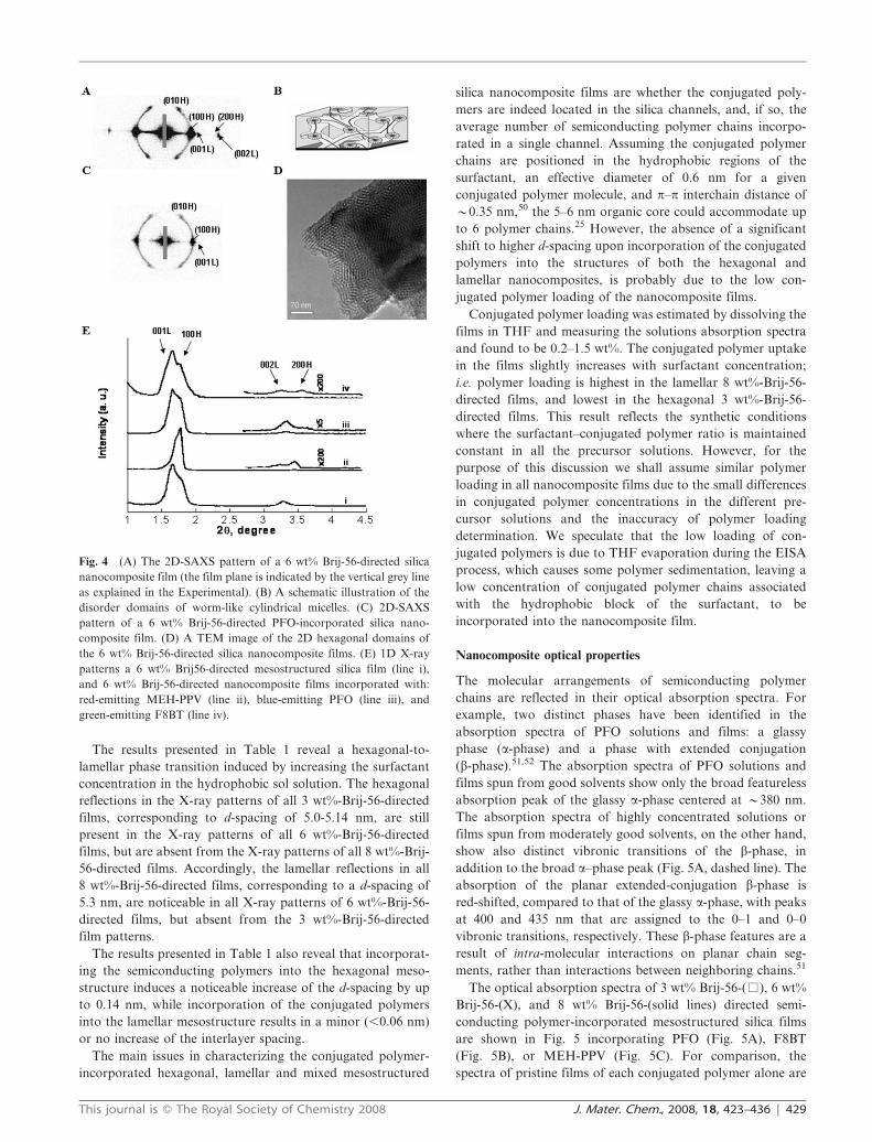
At an intermediate concentration of the structure-directing
surfactant, 6 wt% Brij-56 in the THF-rich sol solution with and
without a conjugated polymer guest species, a mixture of the
2D hexagonal and the lamellar mesostructures is obtained. The
2D-SAXS pattern of the 6 wt% Brij-56-directed mesostruc-
tured silica films, Fig. 4A, shows the same intense (100) and
weaker (010) reflections obtained for the hexagonal 3 wt%
Brij-56-directed mesostructured silica films (Fig. 2A),39,44
together with the (001) and (002) reflection obtained for the
lamellar 8 wt% Brij-56-directed mesostructured silica films
(Fig. 3A).44 In addition to the mixture of the hexagonal and
lamellar reflections, the 2D-SAXS pattern also shows signifi-
cant amounts of the disordered worm-like cylindrical domains,
schematically illustrated in Fig. 4B. The presence of the worm-
like phase is evident from the strong diffraction arcs super-
imposed on the hexagonal and lamellar spot pattern.
The mixture of phases is also obtained for the conjugated
polymer-incorporated 6 wt% Brij-56-directed silica nanocom-
posite films. Fig. 4C shows the presence of the mixed phases in
the 2D-SAXS pattern of the PFO-incorporated 6 wt% Brij-56-
directed silica nanocomposite films. Similar patterns were
obtained for F8BT- and MEH-PPV-incorporated 6 wt%
Brij-56-directed silica nanocomposite films (not shown). In
summary, all 6 wt% Brij-56-directed silica nanocomposite
films, without and with conjugated polymer, appear to consist
of a mixture of three mesostructures: i) 2D hexagonal domains
with cylindrical orientations predominantly parallel to the
substrate, as shown in the TEM image (Fig. 4D); ii) worm-like
aggregates without appreciable orientational order; and iii)
lamellar regions with the lamellae parallel to the substrate.
The combination of the hexagonal and lamellar phases is
also evident from the 1D X-ray patterns (Fig. 4E). The 1D
XRD patterns of 6 wt% Brij-56-directed silica film without
semiconducting polymer guests and with MEH-PPV, PFO, or
F8BT incorporated are shown in Fig. 4E, lines i, ii, iii, and iv,
respectively. These patterns are in agreement with the 2D
SAXS results showing a combination of the hexagonal (100)
and (200) reflections with a lattice parameter of y5.0 nm,
and the (001) and (002) reflections of the lamellar mesophase
with a basal spacing of y5.3 nm. The hexagonal lattice
parameters and lamellar basal spacing values of the 6 wt%
Brij-56-directed silica films without and with semiconducting
polymer guests, calculated from the 1D X-ray patterns in
Fig. 4E are listed in Table 1.
Table 1 Hexagonal lattice parameters and lamellar basal spacing values of the 3, 6 and 8 wt% Brij-56-directed mesostructured silica films, and 3, 6and 8 wt% Brij-56-directed semiconducting polymer-incorporated silica mesostructured films, calculated from the 1D X-ray patterns presented inFig. 2E, 3E and 4E
Amount ofBrij-56 insol/wt%
Semiconductingpolymer
2h (hexagonal),(100)/(200)degree
d-spacing(hexagonal)(100)/(200)/A
2h (lamellar)(001)/(002)degree
d-spacing(lamellar)(001)/(002)/A Mesophase
3 None 1.77/3.36 49.92/26.30 — — Hexagonal3 MEHPPV 1.75/3.50 50.49/25.25 — — Hexagonal3 PFO 1.75/3.50 50.49/25.25 — — Hexagonal3 F8BT 1.72/3.44 51.37/25.69 — — Hexagonal6 None 1.77/3.36 49.92/26.30 1.66/3.32 53.22/26.62 Mixed6 MEHPPV 1.77/3.36 49.92/26.30 1.68/3.36 52.59/26.29 Mixed6 PFO 1.73/3.46 51.07/25.91 1.65/3.30 53.54/26.77 Mixed6 F8BT 1.76/3.52 50.20/25.10 1.65/3.30 53.54/26.77 Mixed8 None — — 1.67/3.34 52.91/26.46 Lamellar8 MEHPPV — — 1.67/3.34 52.91/26.46 Lamellar8 PFO — — 1.66/3.32 53.22/26.62 Lamellar8 F8BT — — 1.65/3.30 53.54/26.77 Lamellar
Fig. 3 (A) The 2D-SAXS pattern of a 8 wt% Brij-56-directed silica
nanocomposite film (the film plane is indicated by the vertical grey line
as explained in the Experimental). (B) A schematic illustration of the
lamellar mesostructure with the lamellae oriented parallel to the
substrate. (C) The 2D-SAXS pattern of an 8 wt% Brij-56-directed
PFO-incorporated silica nanocomposite film. (D) A TEM image of the
lamellar 8 wt% Brij-56-directed mesostructured silica film. (E) 1D
X-ray patterns of 8 wt% Brij56-directed mesostructured silica film
(line i), and 8 wt% Brij-56-directed nanocomposite films incorporated
with: red-emitting MEH-PPV (line ii), blue-emitting PFO (line iii), and
green-emitting F8BT (line iv).
428 | J. Mater. Chem., 2008, 18, 423–436 This journal is � The Royal Society of Chemistry 2008
The results presented in Table 1 reveal a hexagonal-to-
lamellar phase transition induced by increasing the surfactant
concentration in the hydrophobic sol solution. The hexagonal
reflections in the X-ray patterns of all 3 wt%-Brij-56-directed
films, corresponding to d-spacing of 5.0-5.14 nm, are still
present in the X-ray patterns of all 6 wt%-Brij-56-directed
films, but are absent from the X-ray patterns of all 8 wt%-Brij-
56-directed films. Accordingly, the lamellar reflections in all
8 wt%-Brij-56-directed films, corresponding to a d-spacing of
5.3 nm, are noticeable in all X-ray patterns of 6 wt%-Brij-56-
directed films, but absent from the 3 wt%-Brij-56-directed
film patterns.
The results presented in Table 1 also reveal that incorporat-
ing the semiconducting polymers into the hexagonal meso-
structure induces a noticeable increase of the d-spacing by up
to 0.14 nm, while incorporation of the conjugated polymers
into the lamellar mesostructure results in a minor (,0.06 nm)
or no increase of the interlayer spacing.
The main issues in characterizing the conjugated polymer-
incorporated hexagonal, lamellar and mixed mesostructured
silica nanocomposite films are whether the conjugated poly-
mers are indeed located in the silica channels, and, if so, the
average number of semiconducting polymer chains incorpo-
rated in a single channel. Assuming the conjugated polymer
chains are positioned in the hydrophobic regions of the
surfactant, an effective diameter of 0.6 nm for a given
conjugated polymer molecule, and p–p interchain distance of
y0.35 nm,50 the 5–6 nm organic core could accommodate up
to 6 polymer chains.25 However, the absence of a significant
shift to higher d-spacing upon incorporation of the conjugated
polymers into the structures of both the hexagonal and
lamellar nanocomposites, is probably due to the low con-
jugated polymer loading of the nanocomposite films.
Conjugated polymer loading was estimated by dissolving the
films in THF and measuring the solutions absorption spectra
and found to be 0.2–1.5 wt%. The conjugated polymer uptake
in the films slightly increases with surfactant concentration;
i.e. polymer loading is highest in the lamellar 8 wt%-Brij-56-
directed films, and lowest in the hexagonal 3 wt%-Brij-56-
directed films. This result reflects the synthetic conditions
where the surfactant–conjugated polymer ratio is maintained
constant in all the precursor solutions. However, for the
purpose of this discussion we shall assume similar polymer
loading in all nanocomposite films due to the small differences
in conjugated polymer concentrations in the different pre-
cursor solutions and the inaccuracy of polymer loading
determination. We speculate that the low loading of con-
jugated polymers is due to THF evaporation during the EISA
process, which causes some polymer sedimentation, leaving a
low concentration of conjugated polymer chains associated
with the hydrophobic block of the surfactant, to be
incorporated into the nanocomposite film.
Nanocomposite optical properties
The molecular arrangements of semiconducting polymer
chains are reflected in their optical absorption spectra. For
example, two distinct phases have been identified in the
absorption spectra of PFO solutions and films: a glassy
phase (a-phase) and a phase with extended conjugation
(b-phase).51,52 The absorption spectra of PFO solutions and
films spun from good solvents show only the broad featureless
absorption peak of the glassy a-phase centered at y380 nm.
The absorption spectra of highly concentrated solutions or
films spun from moderately good solvents, on the other hand,
show also distinct vibronic transitions of the b-phase, in
addition to the broad a–phase peak (Fig. 5A, dashed line). The
absorption of the planar extended-conjugation b-phase is
red-shifted, compared to that of the glassy a-phase, with peaks
at 400 and 435 nm that are assigned to the 0–1 and 0–0
vibronic transitions, respectively. These b-phase features are a
result of intra-molecular interactions on planar chain seg-
ments, rather than interactions between neighboring chains.51
The optical absorption spectra of 3 wt% Brij-56-(%), 6 wt%
Brij-56-(X), and 8 wt% Brij-56-(solid lines) directed semi-
conducting polymer-incorporated mesostructured silica films
are shown in Fig. 5 incorporating PFO (Fig. 5A), F8BT
(Fig. 5B), or MEH-PPV (Fig. 5C). For comparison, the
spectra of pristine films of each conjugated polymer alone are
Fig. 4 (A) The 2D-SAXS pattern of a 6 wt% Brij-56-directed silica
nanocomposite film (the film plane is indicated by the vertical grey line
as explained in the Experimental). (B) A schematic illustration of the
disorder domains of worm-like cylindrical micelles. (C) 2D-SAXS
pattern of a 6 wt% Brij-56-directed PFO-incorporated silica nano-
composite film. (D) A TEM image of the 2D hexagonal domains of
the 6 wt% Brij-56-directed silica nanocomposite films. (E) 1D X-ray
patterns a 6 wt% Brij56-directed mesostructured silica film (line i),
and 6 wt% Brij-56-directed nanocomposite films incorporated with:
red-emitting MEH-PPV (line ii), blue-emitting PFO (line iii), and
green-emitting F8BT (line iv).
This journal is � The Royal Society of Chemistry 2008 J. Mater. Chem., 2008, 18, 423–436 | 429
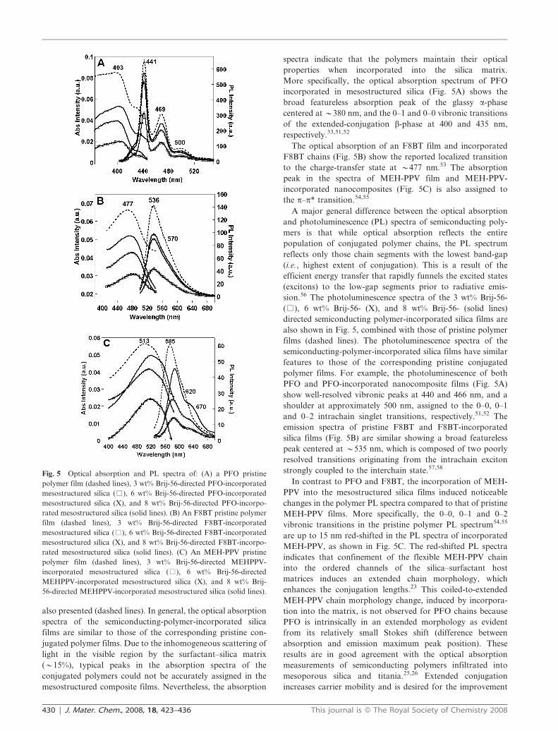
also presented (dashed lines). In general, the optical absorption
spectra of the semiconducting-polymer-incorporated silica
films are similar to those of the corresponding pristine con-
jugated polymer films. Due to the inhomogeneous scattering of
light in the visible region by the surfactant–silica matrix
(y15%), typical peaks in the absorption spectra of the
conjugated polymers could not be accurately assigned in the
mesostructured composite films. Nevertheless, the absorption
spectra indicate that the polymers maintain their optical
properties when incorporated into the silica matrix.
More specifically, the optical absorption spectrum of PFO
incorporated in mesostructured silica (Fig. 5A) shows the
broad featureless absorption peak of the glassy a-phase
centered at y380 nm, and the 0–1 and 0–0 vibronic transitions
of the extended-conjugation b-phase at 400 and 435 nm,
respectively.33,51,52
The optical absorption of an F8BT film and incorporated
F8BT chains (Fig. 5B) show the reported localized transition
to the charge-transfer state at y477 nm.53 The absorption
peak in the spectra of MEH-PPV film and MEH-PPV-
incorporated nanocomposites (Fig. 5C) is also assigned to
the p–p* transition.54,55
A major general difference between the optical absorption
and photoluminescence (PL) spectra of semiconducting poly-
mers is that while optical absorption reflects the entire
population of conjugated polymer chains, the PL spectrum
reflects only those chain segments with the lowest band-gap
(i.e., highest extent of conjugation). This is a result of the
efficient energy transfer that rapidly funnels the excited states
(excitons) to the low-gap segments prior to radiative emis-
sion.56 The photoluminescence spectra of the 3 wt% Brij-56-
(%), 6 wt% Brij-56- (X), and 8 wt% Brij-56- (solid lines)
directed semiconducting polymer-incorporated silica films are
also shown in Fig. 5, combined with those of pristine polymer
films (dashed lines). The photoluminescence spectra of the
semiconducting-polymer-incorporated silica films have similar
features to those of the corresponding pristine conjugated
polymer films. For example, the photoluminescence of both
PFO and PFO-incorporated nanocomposite films (Fig. 5A)
show well-resolved vibronic peaks at 440 and 466 nm, and a
shoulder at approximately 500 nm, assigned to the 0–0, 0–1
and 0–2 intrachain singlet transitions, respectively.51,52 The
emission spectra of pristine F8BT and F8BT-incorporated
silica films (Fig. 5B) are similar showing a broad featureless
peak centered at y535 nm, which is composed of two poorly
resolved transitions originating from the intrachain exciton
strongly coupled to the interchain state.57,58
In contrast to PFO and F8BT, the incorporation of MEH-
PPV into the mesostructured silica films induced noticeable
changes in the polymer PL spectra compared to that of pristine
MEH-PPV films. More specifically, the 0–0, 0–1 and 0–2
vibronic transitions in the pristine polymer PL spectrum54,55
are up to 15 nm red-shifted in the PL spectra of incorporated
MEH-PPV, as shown in Fig. 5C. The red-shifted PL spectra
indicates that confinement of the flexible MEH-PPV chain
into the ordered channels of the silica–surfactant host
matrices induces an extended chain morphology, which
enhances the conjugation lengths.23 This coiled-to-extended
MEH-PPV chain morphology change, induced by incorpora-
tion into the matrix, is not observed for PFO chains because
PFO is intrinsically in an extended morphology as evident
from its relatively small Stokes shift (difference between
absorption and emission maximum peak position). These
results are in good agreement with the optical absorption
measurements of semiconducting polymers infiltrated into
mesoporous silica and titania.25,26 Extended conjugation
increases carrier mobility and is desired for the improvement
Fig. 5 Optical absorption and PL spectra of: (A) a PFO pristine
polymer film (dashed lines), 3 wt% Brij-56-directed PFO-incorporated
mesostructured silica (%), 6 wt% Brij-56-directed PFO-incorporated
mesostructured silica (X), and 8 wt% Brij-56-directed PFO-incorpo-
rated mesostructured silica (solid lines). (B) An F8BT pristine polymer
film (dashed lines), 3 wt% Brij-56-directed F8BT-incorporated
mesostructured silica (%), 6 wt% Brij-56-directed F8BT-incorporated
mesostructured silica (X), and 8 wt% Brij-56-directed F8BT-incorpo-
rated mesostructured silica (solid lines). (C) An MEH-PPV pristine
polymer film (dashed lines), 3 wt% Brij-56-directed MEHPPV-
incorporated mesostructured silica (%), 6 wt% Brij-56-directed
MEHPPV-incorporated mesostructured silica (X), and 8 wt% Brij-
56-directed MEHPPV-incorporated mesostructured silica (solid lines).
430 | J. Mater. Chem., 2008, 18, 423–436 This journal is � The Royal Society of Chemistry 2008
of polymer devices, such as light-emitting diodes and field-
effect transistors.
Additional properties highly desired for plastic electronics in
general, and light-emitting devices specifically, are chemical
and environmental stability. The photochemical stability of the
PFO incorporated into the silica matrix is investigated by
comparing the PL spectra of a pristine PFO film to that of a
PFO-incorporated silica nanocomposite film upon exposure to
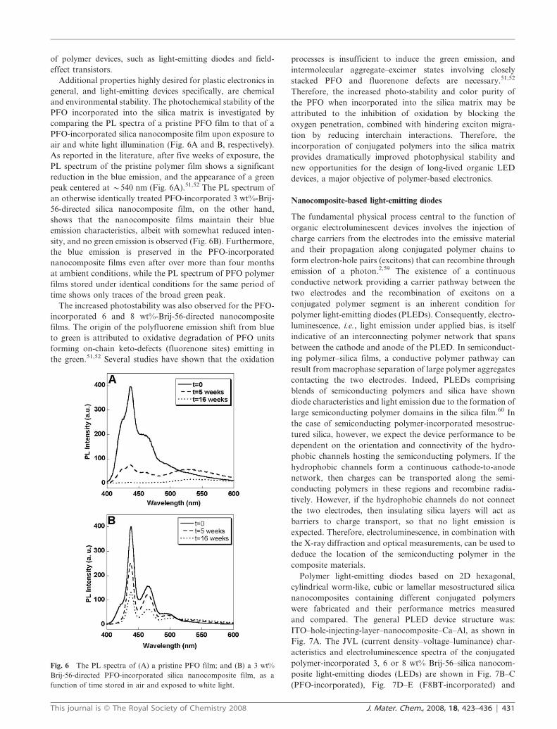
air and white light illumination (Fig. 6A and B, respectively).
As reported in the literature, after five weeks of exposure, the
PL spectrum of the pristine polymer film shows a significant
reduction in the blue emission, and the appearance of a green
peak centered at y540 nm (Fig. 6A).51,52 The PL spectrum of
an otherwise identically treated PFO-incorporated 3 wt%-Brij-
56-directed silica nanocomposite film, on the other hand,
shows that the nanocomposite films maintain their blue
emission characteristics, albeit with somewhat reduced inten-
sity, and no green emission is observed (Fig. 6B). Furthermore,
the blue emission is preserved in the PFO-incorporated
nanocomposite films even after over more than four months
at ambient conditions, while the PL spectrum of PFO polymer
films stored under identical conditions for the same period of
time shows only traces of the broad green peak.
The increased photostability was also observed for the PFO-
incorporated 6 and 8 wt%-Brij-56-directed nanocomposite
films. The origin of the polyfluorene emission shift from blue
to green is attributed to oxidative degradation of PFO units
forming on-chain keto-defects (fluorenone sites) emitting in
the green.51,52 Several studies have shown that the oxidation
processes is insufficient to induce the green emission, and
intermolecular aggregate–excimer states involving closely
stacked PFO and fluorenone defects are necessary.51,52
Therefore, the increased photo-stability and color purity of
the PFO when incorporated into the silica matrix may be
attributed to the inhibition of oxidation by blocking the
oxygen penetration, combined with hindering exciton migra-
tion by reducing interchain interactions. Therefore, the
incorporation of conjugated polymers into the silica matrix
provides dramatically improved photophysical stability and
new opportunities for the design of long-lived organic LED
devices, a major objective of polymer-based electronics.
Nanocomposite-based light-emitting diodes
The fundamental physical process central to the function of
organic electroluminescent devices involves the injection of
charge carriers from the electrodes into the emissive material
and their propagation along conjugated polymer chains to
form electron-hole pairs (excitons) that can recombine through
emission of a photon.2,59 The existence of a continuous
conductive network providing a carrier pathway between the
two electrodes and the recombination of excitons on a
conjugated polymer segment is an inherent condition for
polymer light-emitting diodes (PLEDs). Consequently, electro-
luminescence, i.e., light emission under applied bias, is itself
indicative of an interconnecting polymer network that spans
between the cathode and anode of the PLED. In semiconduct-
ing polymer–silica films, a conductive polymer pathway can
result from macrophase separation of large polymer aggregates
contacting the two electrodes. Indeed, PLEDs comprising
blends of semiconducting polymers and silica have shown
diode characteristics and light emission due to the formation of
large semiconducting polymer domains in the silica film.60 In
the case of semiconducting polymer-incorporated mesostruc-
tured silica, however, we expect the device performance to be
dependent on the orientation and connectivity of the hydro-
phobic channels hosting the semiconducting polymers. If the
hydrophobic channels form a continuous cathode-to-anode
network, then charges can be transported along the semi-
conducting polymers in these regions and recombine radia-
tively. However, if the hydrophobic channels do not connect
the two electrodes, then insulating silica layers will act as
barriers to charge transport, so that no light emission is
expected. Therefore, electroluminescence, in combination with
the X-ray diffraction and optical measurements, can be used to
deduce the location of the semiconducting polymer in the
composite materials.
Polymer light-emitting diodes based on 2D hexagonal,
cylindrical worm-like, cubic or lamellar mesostructured silica
nanocomposites containing different conjugated polymers
were fabricated and their performance metrics measured
and compared. The general PLED device structure was:
ITO–hole-injecting-layer–nanocomposite–Ca–Al, as shown in
Fig. 7A. The JVL (current density–voltage–luminance) char-
acteristics and electroluminescence spectra of the conjugated
polymer-incorporated 3, 6 or 8 wt% Brij-56–silica nanocom-
posite light-emitting diodes (LEDs) are shown in Fig. 7B–C
(PFO-incorporated), Fig. 7D–E (F8BT-incorporated) and
Fig. 6 The PL spectra of (A) a pristine PFO film; and (B) a 3 wt%
Brij-56-directed PFO-incorporated silica nanocomposite film, as a
function of time stored in air and exposed to white light.
This journal is � The Royal Society of Chemistry 2008 J. Mater. Chem., 2008, 18, 423–436 | 431
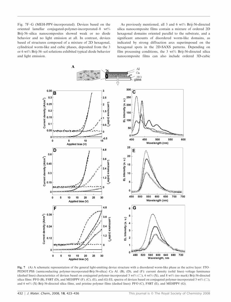
Fig. 7F–G (MEH-PPV-incorporated). Devices based on the
oriented lamellar conjugated-polymer-incorporated–8 wt%
Brij-56–silica nanocomposites showed weak or no diode
behavior and no light emission at all. In contrast, devices
based of structures composed of a mixture of 2D hexagonal,
cylindrical worm-like and cubic phases, deposited from the 3
or 6 wt% Brij-56–sol solutions exhibited typical diode behavior
and light emission.
As previously mentioned, all 3 and 6 wt% Brij-56-directed
silica nanocomposite films contain a mixture of ordered 2D
hexagonal domains oriented parallel to the substrate, and a
significant amounts of disordered worm-like domains, as
indicated by strong diffraction arcs superimposed on the
hexagonal spots in the 2D-SAXS patterns. Depending on
film processing conditions, the 3 wt% Brij-56-directed silica
nanocomposite films can also include ordered 3D-cubic
Fig. 7 (A) A schematic representation of the general light-emitting device structure with a disordered worm-like phase as the active layer: ITO–
PEDOT:PSS–{semiconducting polymer-incorporated-Brij-56-silica}–Ca–Al. (B), (D), and (F): current density (solid lines)–voltage–luminance
(dashed lines) characteristics of devices based on conjugated polymer-incorporated 3 wt% (%), 6 wt% (X), and 8 wt% (no mark) Brij-56-directed
silica films: PFO (B), F8BT (D), and MEHPPV (F). (C), (E), and (G) EL spectra of devices based on conjugated polymer-incorporated 3 wt% (%),
and 6 wt% (X) Brij-56-directed silica films, and pristine polymer films (dashed lines): PFO (C), F8BT (E), and MEHPPV (G).
432 | J. Mater. Chem., 2008, 18, 423–436 This journal is � The Royal Society of Chemistry 2008
domains; while the 6 wt% Brij-56-directed silica nano-
composite lamellar domains, respectively. In contrast, the
8 wt%-Brij-56-directed silica nanocomposite films consist
of the lamellar structure, only, regardless of film-processing
conditions.
Accordingly, we attribute the LED behavior of the semi-
conducting polymer PFO-, F8BT- and MEH-PPV-incorpo-
rated 3 and 6 wt% Brij-56 directed-silica nanocomposites to
the interpenetrating continuous conjugated polymer network
between the two electrodes provided by the worm-like
disordered regions, coexisting with the 2D-hexagonal and
3D-cubic phases. In contrast, in the lamellar silica mesocom-
posite films, the conjugated polymer chains extend parallel to
and are largely insulated from the electrodes by the silica
sheets. As a consequence, the conjugated polymer chains do
not form a continuous network through the film between the
electrodes and thus the lamellar mesocomposite shows no
LED performance whatsoever. The dramatic differences in the
performance of diodes prepared from the different phases
indicate that the conjugated polymer species are indeed
incorporated in the ordered hydrophobic channels of the
nanocomposite host matrix and are neither macroscopically
phase-separated nor distributed randomly within the nano-
structured silica films.
The performance of the conjugated polymer-incorporated 3
and 6 wt% Brij-56–silica nanocomposite light-emitting diodes
are poorer than those of pristine polymer films as summarized
in Table 2. The high fields required for current and light
turn-on in the nanocomposite devices are due to the insulating
character of the silica host matrix, which inhibits charge
transfer, and suggest that carriers are injected from the
electrodes into a thin composite layer adjacent to the electrode,
followed by carrier transport mainly along the polymer chains
and recombination on emissive polymer segments. The much
lower brightness observed for the nanocomposite devices
compared to those of a simple pristine conjugated polymers
PLEDs2,58,61 are the result of the very low polymer content in
the composite film, further limited by abundance of hexagonal
or lamellar domains in the film. This suggestion is further
supported by comparing the LED performances of the
3 wt% Brij-56 directed nanocomposite films to those of the
6 wt% Brij-56 directed nanocomposite films. As mentioned
earlier, the conjugated polymer uptake in the nanocomposite
films corresponds directly to the surfactant concentration, and
hence is higher in the in 6 wt% Brij-56 directed nanocomposite
films than in the 3 wt% Brij-56 directed nanocomposite films.
Consequently, the turn-on voltages, current densities and
brightness of the 6 wt% Brij-56 directed films are higher than
those of the corresponding 3 wt% Brij-56 directed films (Fig. 7
and Table 2), regardless of the type of conjugated polymer
incorporated. We conclude therefore, that the nanocomposites
device performance is currently limited by the low conjugated
polymer loading and only partial presence of interpenetrating
disordered worm-like regions, hence a substantial increase in
conjugated polymer up-take is expected to provide long-lived,
highly luminescent LEDs.
The electroluminescence spectra of the F8BT and MEH-
PPV-incorporated 3 and 6 wt% Brij-56 directed nanocompo-
sites (Fig. 7) generally resemble their corresponding PL spectra
(Fig. 5), and the PL and EL spectra of pristine polymer films
(Fig. 5 and Fig. 7). For example, the EL spectra of F8BT-
incorporated silica nanocomposites (Fig. 7E) exhibit the strong
broad peak at 534 nm and shoulder at 570 nm, also observed
in the nanocomposite PL spectra (Fig. 5B) and the EL spec-
trum of pristine F8BT diodes (Fig. 7E). PFO-incorporation
into the silica matrix, on the other hand, induced noticeable
changes in the EL spectra compared to that of pristine PFO
films. The EL spectrum of a spun pristine PFO diode exhibits a
strong emission peak from the disordered a-phase chains
centered at y420 nm, and weaker shoulders at 440, 476 and
500 nm assigned to the 0–0, 0–1, and 0–2 transitions from
b-phase aggregates, respectively (Fig. 7C). In contrast to the
EL spectrum of pristine polymer films, the EL spectra of
the PFO-incorporated nanocomposite are dominated by the
extended b-phase transitions. The a-phase transition is still
noticeable in the EL spectrum of the PFO-incorporated 3 wt%
Brij-56 directed silica nanocomposite diode (Fig. 7C), but
diminished in the EL spectrum of the higher conjugated
polymer loaded 6 wt% Brij-56 directed nanocomposites
(Fig. 7C). We conclude therefore, that incorporation of the
PFO chains into the nanocomposites induces an extended
chain morphology and polymer aggregation in the silica
channels. Aggregation of the incorporated conjugated polymer
chains in the silica channels is also evident from the red-shifted
photoluminescence (Fig. 5B and 5C) and electroluminescence
(Fig. 7E and 7G) spectra of MEH-PPV-incorporated silica
Table 2 JVL characteristics of nanocomposite and pristine polymer light-emitting diodes averaged over 12 devices of each type. The standarddeviations of nanocomposite device turn-on voltage, luminance and current density were , 8%, 25% and 30%, respectively
Material Vturn on, V Luminance/cd m22 Current density/A m22
Pristine PFO 3.3 20 (at 6.5 V) 4 (at 6.5 V)PFO–3 wt% Brij–silica 10 1.2 (at 16 V) 0.03 (at 16 V)PFO–6 wt% Brij–silica 8 3.0 (at 12 V) 0.35 (at 12 V)PFO–8 wt% Brij–silica — — —Pristine F8BT 3.6 14 (at 7 V) 3.8 (at 7 V)F8BT–3 wt% Brij–silica 18.5 2.8 (at 30 V) 0.05 (at 30 V)F8BT–6 wt% Brij–silica 15.5 4.6 (at 23 V) 0.65 (at 23 V)F8BT–8 wt% Brij–silica — — —Pristine MEH-PPV 4.3 13 (at 8 V) 4.2 (at 8 V)MEH-PPV–3 wt% Brij–silica 18.2 3.1 (at 30 V) 0.21 (at 30 V)MEH-PPV–6 wt% Brij–silica 16 4.3 (at 30 V) 0.4 (at 30 V)MEH-PPV–8 wt% Brij–silica — — —PFO–3 wt% PEO–silica 5.6 5.5 (at 8 V) 0.7 (at 8 V)PFO–6 wt% PEO–silica 4.2 7.6 (at 8 V) 0.8 (at 8 V)PFO–8 wt% PEO–silica 3.7 7.7 (at 8 V) 0.8 (at 8 V)
This journal is � The Royal Society of Chemistry 2008 J. Mater. Chem., 2008, 18, 423–436 | 433
nanocomposite films compared to those of the corresponding
pristine polymer films.
To confirm that the mesostructured nanocomposite device
behavior is governed by the conjugated polymer chains that
are incorporated in the hydrophobic channels of the meso-
structure, and not by conjugated polymer domains macro-
scopically phase-separated in the film, the structure-directing
surfactant in the precursor solution is replaced with a non-
structure-directing polymer: poly(ethylene oxide) (PEO). PEO
is selected because it represents the hydrophilic block of the
surfactant Brij-56, but with the absence of the hydrophobic
block and therefore can not induce the formation of micelles
and liquid-crystalline phases. Consequently, replacing Brij-56
with PEO in the sol solution is expected to promote the
formation of macrophase-separated conjugated polymer
domains in a PEO–silica film. Comparing the optical and
opto-electronic properties of the disordered conjugated poly-
mer–PEO–silica films with those of the corresponding
conjugated polymer incorporated-Brij-56-directed silica nano-
composites, provides the means to associate the device
performance with either incorporated polymer chains, or
phase-separated polymer domains.
The presence of PFO domains in the films deposited
using the synthetic protocol developed for the deposition of
conjugated polymer-incorporated mesostructured silica, but
replacing Brij-56 with PEO, is evident from their optical
absorption and photoluminescence spectra. The absorption
spectra of the PFO–PEO–silica film (ESI{) are noticeably
red-shifted, .10 nm, compared to the absorption spectra of a
pristine PFO film and to PFO-incorporated Brij-56-directed
silica films (Fig. 5A), associated with the increased conjugation
length of PFO chains in aggregated domain. The PL spectra of
PFO–PEO–silica films provide further evidence for PFO
aggregation reflected in the relative intensities of the 440
and 466 nm peaks. The aggregation of PFO chains induces
interchain emission bands that overlap with the principal
intramolecular exciton emission and increase the PL intensity
in the 470–500 nm range.62 The reduced relative intensity
of the 440 and 466 nm peaks in the PL spectrum of the
PFO–8 wt% PEO–silica films (Fig. 8) compared to that in
the PL spectra of pristine PFO films and all mesostructured
PFO-incorporated silica films (Fig. 5A) reflects the contribu-
tions of aggregate transitions in PFO–PEO–silica PL spec-
trum. Similar intermolecular transitions were also observed
in the PL spectra of PFO–3 and 6 wt% PEO–silica films,
indicating that blending PEO, silica and PFO results in the
formation of large PFO aggregates. The significant differences
between the optical properties of PFO–PEO–silica and PFO–
Brij-56–silica films corroborate that the conjugated polymer
chains are incorporated into the hydrophobic channels of the
surfactant-directed mesostructured silica and not macrophase-
separated into polymer domains in the silica matrix.
Diodes based on the PFO–PEO–silica films all showed
diode behavior and light-emission regardless of the PEO
concentration, in contrast to the Brij-56-directed mesostruc-
tured nanocomposite devices, where the device performance
was crucially dependant on the Brij-56 surfactant concentra-
tion. Representative JVL characteristics and EL spectra of
the PFO–PEO–silica diodes are listed in Table 2 and shown
in Fig. 8, respectively. The reduced turn-on voltages and
improved current densities and brightness of the PFO–PEO–
silica devices compared to the corresponding mesostructured
films are assigned to the presence of large polymer aggregates
in the silica matrix, which provide continuous and efficient
charge-transport routes through the film. Accordingly, the
device characteristics improve with increasing PEO concentra-
tion (and hence PFO concentration, because the PEO–PFO
concentration ratio is kept constant between all samples)
approaching the performance of a pristine PFO LED. The
electroluminescence spectra of the disordered PFO–PEO–silica
films are also dominated by the presence of large conjugated
polymer domains, with an increased contribution of the
aggregate transitions at 470–500 nm, similarly to that observed
in their PL spectra (Fig. 8). The striking optical and opto-
electronic differences between the PEO–PFO–silica blends and
the PFO-incorporated Brij-56-directed silica nanocomposites
confirm that the self-organization of the surfactant leads to the
inclusion of the conjugated polymer species in the hydrophobic
channels of the silica, while the surfactants hydrophilic
segments template the polymerization of silica in liquid-
crystalline phases. The continuous network of semiconducting
polymer species throughout the 3 and 6% Brij-56-directed
silica films enabled the integration of ordered nanocomposites
into electronic devices.
A continuous conjugated polymer network could also
form through defects in the silica walls of the mesostructures.
Porous defects are known to exist in the thin silica walls of
calcined Brij-56-directed 2D-hexagonal films (y1 nm), as
demonstrated by high N2 gas adsorption uptake.45 But,
formation of the continuous polymer-threaded defect network
is not likely to form through the film thickness. Therefore,
intentionally directing a phase with continuous through-film
conductive pathway has allowed the integration of ordered
semiconducting polymer–silica nanocomposites into opto-
electronic devices.
Conclusions
In conclusion, optimization of materials synthesis chemistries
and mesophase self-assembly processes, allow new hierarchical
Fig. 8 The PL spectrum of a PFO–8 wt% PEO–silica nanocomposite
film (dashed line), and EL spectra of PFO/3 wt% (%), 6 wt% (X) and
8 wt% (solid line) PEO–silica LEDs.
434 | J. Mater. Chem., 2008, 18, 423–436 This journal is � The Royal Society of Chemistry 2008
structures of mesostructured silica–surfactant–semiconducting
polymer nanocomposites to be tailored for electronic and
opto-electronic applications. Incorporation of the semicon-
ducting polymers into an inorganic matrix can not only endow
the polymer with improved environmental and chemical
stability, but might also induce beneficial properties for
desired applications such as polarized emission. According
to the selection of different surface-active agents, inorganic
precursor species, conjugated polymer solutes, and, crucially,
mutually compatible non-aqueous solvents, it was possible to
prepare preferentially 2D hexagonally ordered or lamellar
mesophase silica with semiconducting polymer guest species
incorporated within the hydrophobic channels. The con-
tinuous network of semiconducting polymer species through-
out the silica mesostructure enabled the integration of ordered
nanocomposites into electronic devices. This was demon-
strated by the separate fabrication of red, green, or blue
nanocomposite LEDs comprising blue PFO-, green F8BT-, or
red MEH-PPV polymer-incorporated partially aligned silica
mesostructures. The nanocomposite device performance is
currently limited by the low conjugated polymer loading and
only partial presence of active interpenetrating disordered
worm-like regions in the film. A substantial increase of the
conjugated polymer uptake into a worm-like or cubically-
ordered film, with continuous through-film organic and
inorganic networks, is expected to yield long-lived, highly
luminescent LEDs. The non-aqueous approach presented here
for the preparation of optically responsive semiconducting
polymer-incorporated mesostructured inorganic host matrices
is expected to be general and extendable to other hybrid
material compositions and structures.
Acknowledgements
This project was funded by the United States–Israel Binational
Science Foundation, grant number 2002134. GLF is a Landau
Fellow, supported by the Taub and Shalom Foundations. CJB
is supported through DOE Basic Energy Sciences, AFOSR
and ARO.
References
1 J. H. Burroughes, D. D. C. Bradley, A. R. Brown, R. N. Marks,K. Mackay, R. H. Friend, P. L. Burns and A. B. Holmes, Nature,1990, 347, 539.
2 R. H. Friend, R. W. Gymer, A. B. Holmes, J. H. Burroughes,R. N. Marks, C. Taliani, D. D. C. Bradley, D. A. Dos Santos, J. L.Bredas, M. Logdlund and W. R. Salaneck, Nature, 1999, 397, 121.
3 G. Horowitz, Adv. Mater., 1998, 10, 365.4 C. D. Dimitrakopoulos and P. R. L. Malenfant, Adv. Mater., 2002,
14, 99.5 M. D. McGehee and A. J. Heeger, Adv. Mater., 2000, 12, 1655.6 J. J. M. Halls, C. A. Walsh, N. C. Greenham, E. A. Marseglia,
R. H. Friend, S. C. Moratti and A. B. Holmes, Nature, 1995, 376,498.
7 K. M. Coakley and M. D. McGehee, Chem. Mater., 2004, 16, 4533.8 G. Yu, J. Gao, J. C. Hummelen, F. Wudl and A. J. Heeger,
Science, 1995, 270, 1789.9 F. Mammeri, E. Le Bourhis, L. Rozes and C. Sanchez, J. Mater.
Chem., 2005, 15, 3787.10 E. Bourgeat-Lami, J. Nanosci. Nanotechnol., 2002, 2, 1.11 H. Colfen and S. Mann, Angew. Chem., Int. Ed., 2003, 42, 2350.12 C. Sanchez, B. Julian, P. Belleville and M. Popall, J. Mater. Chem.,
2005, 15, 3559.
13 R. Gangopadhyay and A. De, Chem. Mater., 2000, 12, 2064.14 C. O. Oriakhi, J. Chem. Educ., 2000, 77, 1138.15 C. Sanchez, B. Lebeau, F. Chaput and J. P. Boilot, Adv. Mater.,
2003, 15, 1969.16 B. Dunn and J. I. Zink, Sol-Gel Technol. Glass Prod. Users, 2004,
355.17 P. N. Minoofar, R. Hernandez, S. Chia, B. Dunn, J. I. Zink and
A. C. Franville, J. Am. Chem. Soc., 2002, 124, 14388.18 R. Hernandez, A. C. Franville, P. Minoofar, B. Dunn and J. I. Zink,
J. Am. Chem. Soc., 2001, 123, 1248.19 T. Keeling-Tucker and J. D. Brennan, Chem. Mater., 2001, 13,
3331.20 N. A. Melosh, C. A. Steinbeck, B. J. Scott, R. C. Hayward,
P. Davidson, G. D. Stucky and B. F. Chmelka, J. Phys. Chem. B,2004, 108, 11909.
21 P. D. Yang, G. Wirnsberger, H. C. Huang, S. R. Cordero,M. D. McGehee, B. Scott, T. Deng, G. M. Whitesides,B. F. Chmelka, S. K. Buratto and G. D. Stucky, Science, 2000,287, 465.
22 T. D. de Morais, F. Chaput, K. Lahlil and J. P. Boilot, Adv.Mater., 1999, 11, 107.
23 T. Q. Nguyen, J. J. Wu, V. Doan, B. J. Schwartz and S. H. Tolbert,Science, 2000, 288, 652.
24 T. Q. Nguyen, J. Wu, S. H. Tolbert and B. J. Schwartz, Adv.Mater., 2001, 13, 609.
25 J. J. Wu, A. F. Gross and S. H. Tolbert, J. Phys. Chem. B, 1999,103, 2374.
26 K. M. Coakley, Y. X. Liu, M. D. McGehee, K. L. Frindell andG. D. Stucky, Adv. Funct. Mater., 2003, 13, 301.
27 Y. F. Lu, Y. Yang, A. Sellinger, M. C. Lu, J. M. Huang, H. Y. Fan,R. Haddad, G. Lopez, A. R. Burns, D. Y. Sasaki, J. Shelnutt andC. J. Brinker, Nature, 2001, 410, 913.
28 A. G. Pattantyus-Abraham and M. O. Wolf, Chem. Mater., 2004,16, 2180.
29 M. Alvaro, A. Corma, B. Ferrer, M. S. Galletero, H. Garcia andE. Peris, Chem. Mater., 2004, 16, 2142.
30 B. McCaughey, C. Costello, D. H. Wang, J. E. Hampsey,Z. Z. Yang, C. J. Li, C. J. Brinker and Y. F. Lu, Adv. Mater.,2003, 15, 1266.
31 Y. F. Lu, R. Ganguli, C. A. Drewien, M. T. Anderson,C. J. Brinker, W. L. Gong, Y. X. Guo, H. Soyez, B. Dunn,M. H. Huang and J. I. Zink, Nature, 1997, 389, 364.
32 C. J. Brinker, Y. F. Lu, A. Sellinger and H. Y. Fan, Adv. Mater.,1999, 11, 579.
33 M. Grell, D. D. C. Bradley, X. Long, T. Chamberlain,M. Inbasekaran, E. P. Woo and M. Soliman, Acta Polym., 1998,49, 439.
34 T. Q. Nguyen, V. Doan and B. J. Schwartz, J. Chem. Phys., 1999,110, 4068.
35 M. Voigt, J. Chappell, T. Rowson, A. Cadby, M. Geoghegan,R. A. L. Jones and D. G. Lidzey, Org. Electron., 2005, 6, 35.
36 D. Grosso, F. Cagnol, G. J. D. A. Soler-Illia, E. L. Crepaldi,H. Amenitsch, A. Brunet-Bruneau, A. Bourgeois and C. Sanchez,Adv. Funct. Mater., 2004, 14, 309.
37 K. Valle, P. Belleville, F. Pereira and C. Sanchez, Nat. Mater.,2006, 5, 107.
38 R. C. Hayward, P. C. A. Alberius, E. J. Kramer and B. F. Chmelka,Langmuir, 2004, 20, 5998.
39 D. Zhao, P. Yang, N. Melosh, J. Feng, B. F. Chmelka andG. D. Stucky, Adv. Mater., 1998, 10, 1380.
40 T. Lee, O. Park, J. Kim, J. Hong and Y. Kim, Chem. Mater., 2001,13, 2217.
41 J. H. Park, Y. T. Lim, O. Park O, J. K. Kim, J. W. Yu andY. C. Kim, Adv. Funct. Mater., 2004, 14, 377.
42 E. Aharon, A. Albo, M. Kalina and G. L. Frey, Adv. Funct.Mater., 2006, 16, 980.
43 M. Klotz, P. A. Albouy, A. Ayral, C. Menager, D. Grosso,A. Van der Lee, V. Cabuil, F. Babonneau and C. Guizard, Chem.Mater., 2000, 12, 1721.
44 P. C. A. Alberius, K. L. Frindell, R. C. Hayward, E. J. Kramer,G. D. Stucky and B. F. Chmelka, Chem. Mater., 2002, 14,3284.
45 B. Smarsly, A. Gibaud, W. Ruland, D. Sturmayr and C. J. Brinker,Langmuir, 2005, 21, 3858.
This journal is � The Royal Society of Chemistry 2008 J. Mater. Chem., 2008, 18, 423–436 | 435
46 D. A. Doshi, A. Gibaud, V. Goletto, M. C. Lu, H. Gerung,B. Ocko, S. M. Han and C. J. Brinker, J. Am. Chem. Soc., 2003,125, 11646.
47 A. Gibaud, D. Grosso, B. Smarsly, A. Baptiste, J. F. Bardeau,F. Babonneau, D. A. Doshi, Z. Chen, C. J. Brinker and C. Sanchez,J. Phys. Chem. B, 2003, 107, 6114.
48 D. Grosso, F. Babonneau, C. Sanchez, G. J. D. A. Soler-Illia,E. L. Crepaldi, P. A. Albouy, H. Amenitsch, A. R. Balkenende andA. Brunet-Bruneau, J. Sol–Gel Sci. Technol., 2003, 26, 561.
49 E. L. Crepaldi, G. J. D. A. Soler-Illia, A. Bouchara, D. Grosso,D. Durand and C. Sanchez, Angew. Chem., Int. Ed., 2003, 42, 347.
50 C. Y. Yang, F. Hide, M. A. Diaz-Garcia, A. J. Heeger and Y. Cao,Polymer, 1998, 39, 2299.
51 S. Gamerith, C. Gadermaier, U. Scherf and E. J. W. List, Phys.Status Solidi A, 2004, 201, 1132.
52 D. Neher, Macromol. Rapid Commun., 2001, 22, 1365.53 K. G. Jespersen, W. J. D. Beenken, Y. Zaushitsyn, A. Yartsev,
M. Andersson, T. Pullerits and V. Sundstrom, J. Chem. Phys.,2004, 121, 12613.
54 P. Wood, I. D. W. Samuel, G. R. Webster and P. L. Burn, Synth.Met., 2001, 119, 571.
55 M. Zheng, F. L. Bai and D. B. Zhu, Polym. Adv. Technol., 1999,10, 476.
56 J. L. Bredas, D. Beljonne, V. Coropceanu and J. Cornil,Chem. Rev., 2004, 104, 4971.
57 C. L. Donley, J. Zaumseil, J. W. Andreasen, M. M. Nielsen,H. Sirringhaus, R. H. Friend and J. S. Kim, J. Am. Chem. Soc.,2005, 127, 12890.
58 J. S. Kim, R. H. Friend, I. Grizzi and J. H. Burroughes, Appl.Phys. Lett., 2005, 87, 023506/1.
59 K. J. Reynolds, J. A. Barker, N. C. Greenham, R. H. Friend andG. L. Frey, J. Appl. Phys., 2002, 92, 7556.
60 J. H. Park, S. Kim, Y. C. Kim and O. O. Park, Nanotechnology,2005, 16, 1793.
61 A. P. Kulkarni and S. A. Jenekhe, Macromolecules, 2003, 36,5285.
62 P. K. H. Ho, J. S. Kim, N. Tessler and R. H. Friend, J. Chem.Phys., 2001, 15, 2709.
436 | J. Mater. Chem., 2008, 18, 423–436 This journal is � The Royal Society of Chemistry 2008


