Embed Size (px)
Citation preview

2740 IEEE TRANSACTIONS ON POWER ELECTRONICS, VOL. 27, NO. 6, JUNE 2012
Space Vector Modulation Strategy Applied toInterphase Transformers-Based Five-Level
Current Source InvertersBruno Scortegagna Dupczak, Student Member, IEEE, Arnaldo Jose Perin, Member, IEEE,
and Marcelo Lobo Heldwein, Member, IEEE
Abstract—This work proposes a space vector modulation (SVM)scheme applied to an interphase transformers-based five-level cur-rent source inverter (IT-MCSI) in order to fulfill the following re-quirements: the reduction of the number of switching transitionsduring a switching period, the doubling of the ripple frequencywith respect to the switching frequency at the input and outputterminals, the balance of the interphase transformers magnetizingvoltages leading to zero average flux in the cores at each switch-ing period, and the use of the full linear modulation range. Theproposed modulation is compared to a conventional phase-shiftedmodulation. The proposal is experimentally tested in a 2.2 kWlab-prototype employing state-of-the-art power components. Theresults verify the theoretical analysis and show that the SVM isable to improve the electrical performance of an IT-MCSI.
Index Terms—Current supplies, inverters, multilevel systems,space vector pulse width modulation.
I. INTRODUCTION
CURRENT source inverters (CSI) have been widely em-ployed in high power medium-voltage (MV) adjustable
speed drives for industrial applications for more than twodecades ago [1]. The electrical performance and efficiency ofCSIs versus that of voltage source inverters (VSI) are frequentlycompared. This comparison typically aims to select the best al-ternative for a given high-power drive system (>1 MW) spec-ification [2], [3]. Despite several advantages offered by VSIs,such as the higher number of industrial drives experiences (reli-ability) and the low semiconductors currents efforts (conversionefficiency), the high dv/dt transients and common-mode (CM)voltages generated with this type of converter often cause harm-ful effects across motor insulation and ball bearings. Assumingthat these are critical issues in certain applications, CSIs thenbecome attractive. This is mainly due to the output capacitorsthat prevent the high di/dt from reaching the machine. The re-sult is the motor being fed with quasi-sinusoidal voltages and
Manuscript received August 12, 2011; revised November 3, 2011; acceptedNovember 14, 2011. Date of current version March 16, 2012. This work wassupported by the Brazilian National Council for Scientific and TechnologicalDevelopment (CNPq) under Grant 558049/2009-5. Recommended for publica-tion by Associate Editor Bin Wu.
The authors are with the Power Electronics Institute (INEP), Elec-trical Engineering Department, Federal University of Santa Catarina(UFSC), Florianopolis, SC, 88040-970, Brazil (e-mail: [email protected];[email protected]; [email protected]).
Color versions of one or more of the figures in this paper are available onlineat http://ieeexplore.ieee.org.
Digital Object Identifier 10.1109/TPEL.2011.2177479
currents. These attributes guarantee that CSIs find their share inthe high power drives market [1], [4].
CSIs are also being investigated in medium to low power ap-plications (1–100 kW). There, the objective is to determine ifthe current source converters are adequate for medium to lowpower AC motor drives. Previous research results have shownthat CSIs typically present lower efficiency figures when com-pared to VSIs. The main reason for this is the higher conductionlosses in the DC-link inductor and power switches. However,the motor losses are reduced for the CSI-fed case. In this con-text, drive systems with CSIs are reported to present similaroverall efficiency [2], [5]. In addition, CSIs voltage boostingcharacteristic is an interesting feature in power-trains for elec-tric/hybrid vehicle applications. This can be beneficial wherethe low voltage supplied by batteries or fuel cells [6] must firstbe boosted by a DC–DC converter prior to being convertedthrough a VSI. Thus, the use of CSIs would provide a more in-tegrated drive system, simultaneously capable of increasing thebattery voltage levels and generating three-phase AC voltagesto feed the machine. Furthermore, the bulky and expensive DCbus capacitor [7], [8] is eliminated. For automotive applications,where high reliability is critical, replacement of capacitors byinductors also contribute to increasing the attainable converteroperation temperature. This is key to integrating motor and elec-tronics cooling systems to lower system costs [9]. The pursuitof higher electrical performance and reduced conversion losseshave led researchers to propose efficient ways to use paral-leled CSIs [10]–[12]. This has generated five-level CSIs that areable to reduce current and voltage ripples and better utilize thepower semiconductors. Therefore, higher power density, due toreduced passive component demands, and better efficiency, dueto lower conduction and switching losses, are achievable. Thiswork uses one such five-level CSI topology considering its po-tential for medium to low power applications. The CSI topologyis based on interphase transformers to provide two DC currentsources at its DC-link.
Medium to low power applications allow the CSIs to useswitching frequencies that are higher than the MV high powerdrives. Therefore, programmed modulation strategies are not asattractive in such applications. Pulse width modulation (PWM)strategies then become an appealing alternative. The first refer-ence deploying PWM in a CSI is from 1972 [13]. Since then,several works have proposed improvements, such as the useof space vector modulation (SVM) strategies [14]–[16]. SVMstrategies are easy to use in digital signal controllers (DSC)
0885-8993/$26.00 © 2011 IEEE

DUPCZAK et al.: SPACE VECTOR MODULATION STRATEGY APPLIED 2741
providing many degrees of freedom to optimize quantities, suchas switching losses, differential mode (DM) emissions, controlbandwidth [1], [15], [17]. Five-level CSIs require modulationstrategies that are specially developed for them. Most of thestrategies presented in the literature are carrier-based PWM,which make use of bilogic to trilogic transforms [18], [19], i.e.,use VSI PWM techniques and convert the resulting switchingpulses to drive a CSI through logic [20].
This work proposes a space vector modulation strategy forinterphase transformers-based five-level current source invert-ers. This is an effort to improve the electrical performance offive-level CSIs used in medium to low power applications. Inaddition to the generation of the fundamental frequency cur-rents, the developed modulation pattern objectives are: 1) re-duction of the number of switching transitions during a switch-ing period; 2) doubling of the ripple frequency with respectto the switching frequency at the input and output terminals;and 3) balance of the interphase transformers magnetizing volt-ages leading to zero average flux in the cores at each switch-ing period; and 4) use of the full linear modulation range.Section II presents the circuit topology, the associated spacecurrent vector representation and an example of a carrier-basedphase-shift modulation with bilogic to trilogic pulses mappingapplied to the five-level CSI. The proposed SVM is presentedin Section III, including the procedures to determine currentvectors duty-cycles, the chosen vector segmentation and theswitching sequences. Simulation results are included and usedto compare both modulation strategies. A 2.2 kW laboratoryprototype is used to verify the performance of the proposedSVM and the main results are given in Section IV. The pro-posed SVM strategy is compared to a conventional three-levelCSI in Section V. Finally, conclusions are presented in SectionVI.
II. FIVE-LEVEL CURRENT SOURCE INVERTER
Among different types of multilevel current source inverters(MCSI) available, the five-level circuit topology that is usedin this work is seen in Fig. 1. The topology requires twelvevoltage bidirectional turn-off switches Sf g , with f = A,B,Cand g = 1 · ·4. It uses two interphase transformers Ti1 and Ti2 ,which provide proper division of the DC-link current. Split in-ductor Lin is responsible for the DC-link current source out-put characteristic. The first references on this structure datefrom the 1980s, employing twelve-pulses modulation [10] andtrapezoidal carriers-based modulation [11]. These works fo-cused very high power variable speed drives and used CSIs ina parallel association. According to [21], this topology resultsfrom the association of single-rating inductor cells and canbe derived with duality principles from the diode-clamp mul-tilevel converter. Proper modulation strategies applied to thistopology guarantee that the interphase transformer cores presentonly switching frequency harmonics and their sidebands and theDC-link inductor can be reduced. The inductor presents low fluxripple and high DC values. This arrangement of the magneticcomponents makes it possible to separate them into directly andinversely highly coupled magnetic elements, allowing optimiza-
Fig. 1. Power system schematic for the three-phase five-level CSI based oninterphase transformers. Reverse blocking IGBTs or series connection of diodesand MOSFETs can be used as voltage bidirectional switches.
tion of their volumes and losses. This has been done for DC–DCconverters in [22], where the principles for dividing a single in-ductor into two magnetic components to be employed in parallelconverters is explained in details. Ferrite can be advantageouslyused in the transformers and higher saturation flux low perme-ability materials, such as iron powder or amorphous materials,in the inductor. In addition, Fig. 1 shows the symmetric distribu-tion of the magnetic elements, which balances impedances andreduces common mode (CM) currents. To ensure the inverter’soutput voltage characteristic, three AC film capacitors Co pro-vide paths for high frequency current circulation and ideallysinusoidal output voltages.
A. MCSI Space Vector Representation
Different from the restrictions imposed upon the modulationof VSIs, where all phase switches are driven in a complemen-tary way to avoid the input voltage source short-circuit, in theCSIs this situation is necessary. It corresponds to energy accu-mulation intervals in the input inductor. Furthermore, a currentcirculation path for the input should be provided at all times.This ensures that the AC-side currents are well defined andprevents overvoltages throughout the circuit.
The switches are divided here into four groups with a singleswitch per phase. The switches are Sf g , where f = {A,B,C}is the phase index and g = {1 · ·4} is the group index. Theswitching functions sf g are defined as
sf g ={
0; if Sf g is OFF+1; if Sf g is ON
. (1)

2742 IEEE TRANSACTIONS ON POWER ELECTRONICS, VOL. 27, NO. 6, JUNE 2012
Thus, to fulfill the modulation restrictions given above it isnecessary that ∑
f ={A,B ,C }sf g = 1. (2)
Considering the constraints for the switching conditions, thefive-level CSI presents 81 valid switching states En . The switch-ing states are represented here with a vector 4 × 1 where eachcomponent corresponds to a switch group. Thus,
En = [f1 f2 f3 f4 ] (3)
with f1...4 ∈ {A,B,C} and n ∈ {01, 02, . . . 81}, where thecapital letters designate which phase is switched on at eachgroup.
The current values flowing through the load phases are deter-mined from the switching states. For instance, given switchingstate [A B B C], the output phase currents are accordingly de-fined with io,A = +Iin/2, io,B = 0 due to the free-wheeling paththrough switches SB 2 and SB 3 and io,C = −Iin/2. Pluggingthe corresponding current values into the vector transformationdefined with
�io =23
[io,Aej0 + io,B ej 2 π
3 + io,C ej 4 π3
](4)
generates the complex current vector �I01 , which is representedby
�I01 =12Iin + j
√3
6Iin . (5)
Applying the same procedure for all switching states gives 19synthesizable current vectors for the five-level CSI. Using thevalue of the input current
(Iin
)to normalize these vectors, i.e.,
dividing all computed vectors by(Iin
)defines the space vectors
depicted in Fig. 2. The switching states that lead to each vectorare also shown.
B. Phase-Shifted Modulation
Interleaved operation of static converters is typically asso-ciated with phase-shifted disposition modulation (PS-PWM).Therefore, the five-level CSI is evaluated with this type ofmodulation in the following. The main objective is to verifyif the benefits of the interleaved operation mode, as well asthe increase of the ripple frequency at the passive elements, isachieved. The gate pulses generated by conventional sinusoidalPS-PWM technique are mapped as seen in Fig. 3 to meet theCSI switching states constraints presented above. This mappingprocess is implemented using the bilogic to trilogic translationprocedure described in [18], [19]. To evaluate the performanceof this modulation strategy, simulations were performed usingthe specifications on Table I. The results at steady state arepresented in Fig. 4. Fig. 4(c) and (g) shows that the PS-PWMmodulation ensures the two main requirements for the converteroperation, i.e., generate five current levels and low harmoniccontents at the load voltages. The converter switching frequency(1/Tsw ) is twice the frequency of the carrier signal, since dou-ble update mode is used in the modulator. Nevertheless, theswitching frequency waveforms in Fig. 4(b) and (d) clarify that
Fig. 2. Switching states and normalized current space vectors (00 up to 18)for the five-level CSI. Switching states are represented by the sequence of lettersaround the vector numbers.
the ripple frequency at the DC current iin and at the phasecurrent io,A is the same as the switching frequency. Therefore,this modulation strategy does not provide the desirable inter-leaving operation mode. Moreover, the io,A zero current levelis observed at regions around the peak of fundamental output
current (im,A ). This indicates that the null vector(�I00
)is being
used unnecessarily. This vector is not adjacent to the trajectorydescribed by the reference vector at the used modulation indexMi = 0.75. Furthermore, the large amplitude of the DC currentripple and the high common mode voltage vN O = VN − VO
seen in Fig. 4(g) are not optimal in any sense.
III. PROPOSED SPACE VECTOR MODULATION
Space vector modulation (SVM) was proposed in the mid-80s [23], with significant advantages in motor drives using VSIsover naturally or regularly sampled sinusoidal PWM (SPWM)modulation. The main SVM characteristic is the high degreeof freedom to properly and directly choose the converter vec-tors to be used in any time instant. This, allied with the choiceof the switching states, opens up a large range of possibili-ties to optimize switching transitions (switching losses), ripplefrequency at passive elements, harmonic content of load cur-rents and voltages, common mode voltages, and the balancingof certain converter parameters, such as the DC-link voltage inmultilevel VSIs.
It is common practice to use αβ or dq reference framesto control static converters, for instance, to perform speed ortorque control in electric motor drives. The switch driver signalsare typically generated through carrier-based PWM modulation

DUPCZAK et al.: SPACE VECTOR MODULATION STRATEGY APPLIED 2743
Fig. 3. (a) Diagram of the five-level CSI, employing two phase-shifted carriers. (b) Pulses generated by conventional sinusoidal PWM technique (X1 , X2 , X3 )lead to CSI pulses (Ya , Yb , Yc ) by bilogic to trilogic linear mapping.
TABLE IFIVE-LEVEL CSI SPECIFICATIONS
strategies (regularly sampled) due to the existence of dedicatedhardware for this purpose in current digital signal controllers.Moreover, for multilevel voltage source inverters (MVSI), SVMcan also be realized in such dedicated DSC peripherals by the ad-dition of a common offset (0-axis) modulation signal to the threephase references in a carrier-based scheme [24]. To employ theDSC carrier-based modulation peripherals in order to performan MCSI modulation scheme is a more complex task. Besidesthe modification of the reference signals, it is also necessaryto realize the switching states mapping process. The bilogic totrilogic is typically employed. An example of such a techniqueis presented in [20], which uses a five-level CSI structure witha Phase Disposition-Based Centered Space Vector Modulation(PD-CSVPWM) plus the tri- to bilogic transformation imple-mented in an FPGA. However, the employed CSV signals areoptimized to reduce the harmonic content in MVSIs. It is notknown if the results are also optimal for the CSI. Furthermore,additional circuitry (the FPGA) is required. Thus, system costis increased.
The approach taken in the following is to perform the five-level CSI modulation in a single chip, using the SVM concept.Thus, based on the vector representation in Fig. 2, an SVMscheme is proposed and switching states are selected aiming to:
1) Use the three nearest current vectors around the referencevector circular path at all times in order to generate outputvoltages and currents with low harmonic contents;
2) Ensure zero local average voltage at the interphase trans-formers windings at each switching period to avoidthe presence of DC or low frequency magnetic fluxesthat could lead them into saturation or increased devicevolume;
3) Provide that the operating frequency of the input inductor(Lin ) and output capacitors (Co ) are twice the switchingfrequency, aiming to reduce the passive elements withoutincreasing the switching losses.
A. Calculation of Duty Cycles by Projections
The primary goal of the space vector modulation is to syn-
thesize a reference vector(�i∗
)from a sampling of the inverter
static current vectors during a switching period, where “sample”is understood as the time at which the converter remains in agiven switching state that generate the vector of interest. Thisrequires the computation of duty cycles for each MCSI currentvector. The duty cycles depend on the modulation index (Mi)and the current reference angle (θ) of �i∗. A general method forcomputing vectors duty cycles for neutral-point clamped MVSIis explained in [25]. This is based on determining given pro-jections of the reference vector, in order to simplify the spacevector modulation process. Looking at Fig. 5(a), if any threevectors are arranged in the αβ plane defining a triangular regionwith vertices ia , ib , and ic , the reference vector �i∗ lying in thisregion can be composed as
�i∗ = �ic + �pa + �pb
�i∗ =|�pa |la
�ia +|�pb |lb
�ib +(
1 − |�pa |la
− |�pb |lb
)�ic (6)

2744 IEEE TRANSACTIONS ON POWER ELECTRONICS, VOL. 27, NO. 6, JUNE 2012
Fig. 4. Five-level CSI global and local simulation results, employing phase-shifted PWM modulation with bilogic to trilogic signals mapping: (a), (b) Inputcurrent (iin ) and interphase transformers currents (ip ,1 to in ,2 ). (c), (d) Switch (iS A 1 ), output (io ,A ) and load (im ,A ) currents. (e), (f) Interphase transformersvoltages. (g), (h) Line-to-line load voltages and common-mode voltage (VN O ).
Fig. 5. (a) Projections and composition of the reference vector from threearbitrary vectors, (b) Projections of current reference vector in the ±π/6 axisat first sextant.
where |�pa | and |�pa | are the module of the projections of �i∗ on thetriangle sides and la , lb are the distances between the adjacentvectors. From (6), the generic vectors duty cycles are
da′ =
|�pa |la
db′ =
|�pb |lb
dc′ = 1 − da
′ − db′. (7)
In the specific case of the five-level CSI, the normalized spaceof Fig. 2 is divided into six triangular sextants (Ns), with the firstsextant shown in Fig. 5(b). Due to the symmetry of the sextantsand aiming to simplify the calculation process, the normalizedcurrent reference vector �i∗ is rotated to the first sextant. Thus,the angle of �i∗ is now represented by θ′, which is defined as
θ′ = θ − (Ns − 1)π
3(8)
where Ns ∈ {1, 2 . . . 6}. Using the edges that define the sextantat Fig. 5(b), two axes where the projections of the referencevector lie are defined with angles equal to ±π/6. The values of
the projections are determined with
|�pa | = Mi
[cos (θ′)√
3− sin (θ′)
](9)
|�pb | = Mi
[cos (θ′)√
3+ sin (θ′)
](10)
where the modulation index takes values between 0 ≤ Mi ≤ 1for the MCSI linear modulation range. Whereas each sextantof the vector plane can be divided into four smaller regions,it is observed that each side of the triangles presents a lengthlT = 1/
√3 (see Fig. 6). This corresponds to the normalized
distance between two adjacent vectors. Using this distance and(9) and (10) in (7), the five-level CSI generic duty cycles aregiven by
da′ =
|�pa |lT
= Mi
[cos (θ′) −
√3 sin (θ′)
](11)
db′ =
|�pb |lT
= Mi
[cos (θ′) +
√3 sin (θ′)
]. (12)
In addition, the generic duty cycles can be used to find the re-gion where the current reference vector is located (see examplesin Fig. 6). The modulation algorithm uses the three vectors thatare at the vertices of this region once this is defined. Therefore,the regions, vectors, and real duty cycles necessary to synthe-size the reference vector, are found by using the comparisonconditions presented on Table II.
B. Vector Segmentation and Switching Sequences
As seen in Fig. 2, each vector is generated by the availableinverter switching states. Switching state redundancy provides

DUPCZAK et al.: SPACE VECTOR MODULATION STRATEGY APPLIED 2745
Fig. 6. Reference vector projections in the four possible regions of the firstsextant. The projection lengths are used to calculate the duty cycles and to definethe closer vectors to synthesize the current vector reference �i∗.
TABLE IICOMPARISON CONDITIONS USED TO DEFINE THE REAL DUTY CYCLES AND
VECTORS EMPLOYED IN THE SVM PROCESS INSIDE THE FIRST SEXTANT
the same voltage values at the input inductor and current onthe inverter output terminals. However, each switching stateuses different switches and applies different voltages at the in-terphase transformer terminals. This is seen with the examplegiven in Fig. 7, where both switching states E20 and E22 gener-ate the current vector �I01 . Considering that the windings of Ti1and Ti2 present the same number of turns, the voltage Vpn is thesame in both switching states, but voltages VT i1 and VT i2 arecomplementary. Thus, the time of application of each vector canbe segmented in equal parts, where a segment for a given currentvector employs different switching states. This is performed toprovide null average voltage value across the interphase trans-formers windings for a complete switching period.
Fig. 7. Switching states E20 and E22 that generate the current vector �I01 .Redundant switching states are used to achieve null local average voltages oninterphase transformers.
Fig. 8. Example of a switching sequence used inside the first sextant/secondregion for the proposed space vector modulation. Letter changing associatedwith each group of switches are highlighted and represent each switch turn-onor turn-off action.
However, the segments can be ordered in time through dif-ferent sequences. The minimization of the number of switchingtransitions is the objective here. Therefore, Fig. 8 presents an ex-ample of segments sequence in accordance with this proposal.This sequence ensures that the switching states are arrangedto provide only one switching period (Tsw ) for each samplingperiod of the vectors (Ts). This is observed by the sequenceof letters associated with each group of switches in Fig. 8. Aspecific letter per group is involved in no more than two tran-sitions either switch turn-ON or turn-OFF. The other switchingsequences, needed to compose the vector modulation in eachspace vector sextant, are presented in Table III.
Moreover, the switching sequence shown in Fig. 8 can beinterpreted as the concatenation of two minor switching se-quences. This causes the current and voltage ripple at the DC-side current and the number of pulses in the inverter outputcurrents to present twice the frequency with respect to the vec-tors sampling (switching) frequency. As the switching states are
2746 IEEE TRANSACTIONS ON POWER ELECTRONICS, VOL. 27, NO. 6, JUNE 2012
TABLE IIISWITCHING STATES SEQUENCES USED TO SYNTHESIZE THE REFERENCE VECTORS IN EACH OF THE SEXTANTS (S) AND REGIONS (R) FOR THE PROPOSED
FIVE-LEVEL CSI SPACE VECTOR MODULATION SCHEME
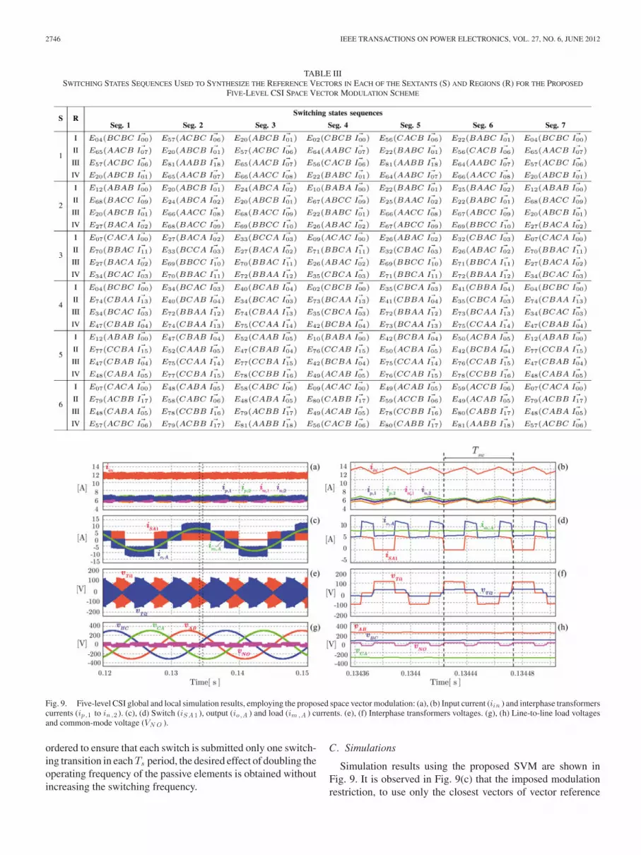
Fig. 9. Five-level CSI global and local simulation results, employing the proposed space vector modulation: (a), (b) Input current (iin ) and interphase transformerscurrents (ip ,1 to in ,2 ). (c), (d) Switch (iS A 1 ), output (io ,A ) and load (im ,A ) currents. (e), (f) Interphase transformers voltages. (g), (h) Line-to-line load voltagesand common-mode voltage (VN O ).
ordered to ensure that each switch is submitted only one switch-ing transition in each Ts period, the desired effect of doubling theoperating frequency of the passive elements is obtained withoutincreasing the switching frequency.
C. Simulations
Simulation results using the proposed SVM are shown inFig. 9. It is observed in Fig. 9(c) that the imposed modulationrestriction, to use only the closest vectors of vector reference

DUPCZAK et al.: SPACE VECTOR MODULATION STRATEGY APPLIED 2747
TABLE IVCOMPARISON OF SIMULATION RESULTS FOR BOTH MODULATIONS
trajectory, modifies the format of the output current levels andthe switches conduction intervals, compared with the results inFig. 4(c). Thus, a significant reduction in input current rippleand common mode voltage values is obtained. A comparison isseen in Table IV and in Fig. 9(a) and (g), respectively. Switchingfrequency details are shown in Fig. 9(b) and (d). The existence oftwo current wave periods of iin and io,a for a single switchingperiod Tsw , is clear. Therefore, the input and output invertercurrents present the first relevant harmonic component at twicethe switching frequency. This is another advantage with respectto PS-PWM modulation. The voltage first frequency componentacross the interphase transformers is the switching frequency.The average value per period is clearly null [see Fig. 9(f)].
Analyzing Table IV shows that the SVM reduces the harmoniccontent of the output current, resulting not only in the reductionof the THD of the current supplied to the load, but additionallythe reduction by roughly one third of the rms values of thecurrents through the AC-side filter capacitors. The reduction ofthe common mode voltage [see Fig. 9(g) and (h)] was not adesign restriction for the proposed SVM. Nevertheless, it is animportant benefit for motor drive applications. The generationof CM voltages in a CSI in mainly due to the voltages acrossthe blocking semiconductors during each of the freewheelingstages of the inverter. In this sense, the proposed SVM is able toapply current vectors that reduce the blocking voltages as seenin Fig. 9(f) and, therefore, able to reduce the CM voltage.
IV. EXPERIMENTAL RESULTS
Experimental results were obtained from a 2.2 kW lab-prototype built as shown in Fig. 10. The five-level CSI bidi-rectional power switches are implemented through the seriesconnection of 650 V CoolMOS (Infineon SPP24N60C3) with600 V SiC diodes (Infineon SDT12S60). The directly coupledDC-side inductor (Lin ) employs a toroidal amorphous core(Amorgreentech APH46P60) and the interphase transformers(Ti1 and Ti2) use ferrite planar cores (Epcos N87 - ELP 43).Texas Instruments floating point TMS320F28335 digital sig-nal controller was used to implement the proposed SVM. TheMCSI output current io,C [see Fig. 11(a)] presents five levels,which high frequency components are filtered out by the out-put capacitors. Thus, low distortion AC currents are generatedas seen through im,C waveform. This waveform was obtained
Fig. 10. Photograph of the built five-level CSI prototype (approximately1 kW/dm3 power density).
at approximately 25% of rated output power, due to the mea-surement apparatus influence on the proper operation of theswitches, i.e., increased loop inductances that cause consider-able overvoltages. However, all other presented waveforms wereobtained at rated power, using a 21 Ω balanced three-phase re-sistive load. Fig. 11(b) shows the total DC-side current iin andthe current sharing at the interphase transformer windings in,2and ip,2 . Appropriate currents balancing is achieved without thepresence of a specific control loop for this purpose. The highfrequency ripple details are depicted in Fig. 11(d), where themain features of the proposed space vector modulation are ob-served. The input current iin ripple frequency presents twicethe switching frequency as seen in the voltage waveform acrossthe switch SA2 . However, the presence of low frequency currentripple is seen at iin in Fig. 11(c). This indicates that furtherimprovements in the implemented modulation process can beperformed mainly on the transitions of reference vector betweenspace vector sextants. The three-phase line-to-line output volt-ages are shown in Fig. 12(a) with an rms value of approximately216.1 V. This value, compared with the 200.8 V average valueof the DC-side voltage, emphasizes the MCSI voltage boostingcapability. Period details of the output voltages are depicted inFig. 12(b). In addition, both interphase transformers voltages(vT i1 , vT i2) present negligible average level [see Fig. 12(c)].This is achieved by the complementary voltage action of thechosen switching states segmentation at each switching period[see Fig. 12(d)].
Experimentally obtained normalized harmonics spectra arepresented on Fig. 13. The first significant harmonic componentsof io,C and iin [Fig. 13(a) and (b), respectively] are at a fre-quency of approximately 40.32 kHz. This is twice the switchingfrequency and shows that another goal of the proposed SVM isaccomplished. The total harmonic distortion (THD) of io,C isapproximately 39.3%. The spectrum of the line-to-line voltagevAB is seen in Fig. 13(c). Despite the presence of low order har-monics, the output voltage THD is lower than 2.3%. The mea-sured rms value of the common mode voltage is vN O
∼= 27.7 V

2748 IEEE TRANSACTIONS ON POWER ELECTRONICS, VOL. 27, NO. 6, JUNE 2012
Fig. 11. (a) Five-level output current (io ,C ) and filtered load current (im ,C ). (b) Input waveforms (vin , iin ) and interphase transformers currents (in ,2 , ip ,2 ).(c),(d) Low and high frequency details of input current (iin ) and voltage across the switch (vS A 2 ).
Fig. 12. (a), (b) Input (vin ) and three-phase line-to-line output voltages (vA B , vB C and vC A ). (c), (d) Low and high frequency details of interphase transformersterminals voltages (vT i1 , vT i2 ).

DUPCZAK et al.: SPACE VECTOR MODULATION STRATEGY APPLIED 2749
Fig. 13. Harmonic spectra (peak values) employing the proposed SVM. (a)Output current (io ,C ). (b) input current (iin ), normalized by the peak valueof the load current fundamental component ( ˆim ,C = 8.7 A). (c) Line-to-lineoutput voltage (vA B ). (d) Common mode voltage (vN O ) normalized by thepeak value of the output line-to-line voltage fundamental component ( ˆvA B =300.0 V).
Fig. 14. Input DC voltage (vin ) and common mode voltage (vN O ).
and its waveform is shown in Fig. 14. Regarding the dynamicresponse with the proposed SVM, the modulation strategy initself is not able to improve the dynamic response of an inverter.However, the proposed SVM allows that smaller passive com-ponents are used given a switching frequency and ripple specifi-cations. Therefore, with smaller passive components, i.e., withlower inductances and capacitances, the dynamic response willbe improved.
V. FIVE-LEVEL CSI PASSIVE COMPONENTS REDUCTION
COMPARED TO A THREE-LEVEL CSI
Typical multilevel converters are associated with high power(MW) applications providing power quality, reducing switch-ing frequency, and increasing overall system-level efficiencyamong other benefits [26]. The objective of the modulationstrategy proposed in this work is to enable a multilevel CSItopology to be employed in medium to low power applications.This is translated as the demand for reduced passive componentssize and weight. This section presents a theoretical analysis ofthe requirements for the magnetic components used in the five-level interphase transformers based CSI (5L-CSI) in comparison
with those of a conventional three-level CSI (3L-CSI) [14]. Itis shown that the sum of the volumes of the interphase trans-former and DC-side inductor is smaller than the volume of asingle magnetic component used in the 3L-CSI. Furthermore,simulation results with the currents for the AC-side capacitorsof both topologies provide evidence that the requirements re-garding rms current values are lessened in the 5L-CSI.
The benchmark requirement for the comparison is the DC-side current ripple (Δiin ), which is defined with
Δiin =Vin − vpn
Lin,totΔtvpn . (13)
Voltage vpn is defined in Fig. 1 for the 5L-CSI and Δtvpn
corresponds to the time duration of a given current vector, whichfinally defines the value of vpn . Assuming that the mutual cou-pling between the inductances Lin is unity, the total DC-sideinductance value is Lin,tot = 4Lin .
In addition, the following assumptions are made:1) The load presents unitary displacement factor (Fd = 1).2) The 5L-CSI operates with a modulation index larger than
Mi >√
3/3. Thus, the reference current vector transitionoccurs only between regions II, III, and IV in the spacevector plane.
3) Based on first sextant analysis, the maximum current rip-ple happens at θ′ = ±π/6 and on the 4th segment of thepulse generation process, where the time of vectors �Ic ( �I06or �I01) are maximum. This time is computed with
Δt4seg =
(1 −
√3Mi
2
)Ts. (14)
4) In θ′ = −π/6 or θ′ = +π/6, the voltage vpn generated byvectors �I06 or �I01 is the the same and given by
vpn ( �I06) =vAB
2= vpn ( �I01) =
vAC
2=
ˆvm,ll
2(15)
which corresponds to the half of the AC line voltage peakvalue ( ˆvm,ll).
5) The idealized 5L-CSI static gain is
Gv =ˆvm,ll
Vin=
2√3MiFd
. (16)
Replacing (14)–(16) into (13), gives
ΔIin,5L =Vin
(1 − 1√
3Mi
) (1 −
√3Mi
2
)Lin,tot
Ts (17)
that allows to calculate the maximum 5L-CSI AC-side currentripple generated with the proposed SVM.
The parameters of Table I (Vin = 200 V, Mi = 0.75,Lin,tot = 4 · 125 μH = 500 μH, and Ts = 1/fs = 49.6 μs)were used to verify (17). The ripple calculated value wasΔIin,5L = 1.6 A, which is very close to the value measuredin the simulations and presented in Table IV.
The maximum DC-side current ripple in a 3L-CSI is causedby the application of the null vector ( �I00). Thus, the voltage

2750 IEEE TRANSACTIONS ON POWER ELECTRONICS, VOL. 27, NO. 6, JUNE 2012
TABLE VCOMPARISON BETWEEN MAGNETIC ELEMENTS DESIGNED
vpn = 0 due to the simultaneous conduction of both switches ina phase leg. Moreover, the null vector maximum time in the firstsextant happens at θ′ = ±π/6 and is defined by (14). Replacingthis value in (13) leads to
ΔIin,3L =Vin
(1 −
√3Mi
2
)Lin,tot
Ts (18)
which defines the maximum 3L-CSI AC-side current ripple,considering a space vector modulation [14]. Assuming the same5L-CSI operation parameters in (18) and specifying a maximumcurrent ripple value of ΔIin,3L = 1.6 A, the resulting value forthe 3L-CSI total DC-side inductance is Lin,tot,3L = 2.17 mH.
The design methodologies presented in [27], [28] are used todesign the inductor and interphase transformers of the 5L-CSIprototype. The same design criteria is used to design the inductorfor a 3L-CSI. Comparative results are presented in Table V,where it is observed that the 5L-CSI magnetics total volume is28.2% lower than the volume of the 3L-CSI inductor. Thus, the5L-CSI structure and the presence of interphase transformerslead to a positive impact on the sizing of the DC-side inductorwhen compared to a 3L-CSI.
The AC-side capacitors also benefit from the five-level op-eration. In this case, simulation results show that, for the sameoperating conditions given in Table I, the rms current valuefor a 3L-CSI capacitors would be 5.0 A, while for the 5L-CSIonly 2.6 A. As the 5L-CSI provides output currents at twicethe frequency pulses of the 3L-CSI, for the same voltage ripple,the value of capacitance for a given voltage ripple can also bereduced as exemplarily reported in [11].
VI. CONCLUSION
A novel SVM strategy has been proposed that allows theinterphase transformer-based five-level CSI to generate highquality output voltages, while reducing the requirements for theemployed passive components, including the coupled magneticcomponents. Therewith, the passive components volume couldbe reduced, providing higher power density levels with good in-verter performance. Experimental results validate the proposedSVM scheme. A brief comparison with a conventional 3L-CSIshows that the 5L-CSI employing the proposed SVM is able toachieve the reduction of the passive component requirements.
ACKNOWLEDGMENT
The authors express their gratitude to the Tractebel EnergiaS/A R&D program for motivation and interest in this work.
REFERENCES
[1] B. Wu, J. Pontt, J. Rodrıguez, S. Bernet, and S. Kouro, “Current-sourceconverter and cycloconverter topologies for industrial medium-voltagedrives,” IEEE Trans. Ind. Electron., vol. 55, no. 7, pp. 2786–2797, Jul.2008.
[2] Y. Suh, J. Steinke, and P. Steimer, “Efficiency comparison of voltage-source and current-source drive systems for medium-voltage applica-tions,” IEEE Trans. Ind. Electron., vol. 54, no. 5, pp. 2521–2531, Oct.2007.
[3] E. Wiechmann, P. Aqueveque, R. Burgos, and J. Rodriguez, “On theefficiency of voltage source and current source inverters for high-powerdrives,” IEEE Trans. Ind. Electron., vol. 55, no. 4, pp. 1771–1782, Apr.2008.
[4] Y. Li, M. Pande, N. Zargari, and B. Wu, “An input power factor controlstrategy for high-power current-source induction motor drive with activefront-end,” IEEE Trans. Power Electron., vol. 25, no. 2, pp. 352–359,Feb. 2010.
[5] V. Colli, P. Cancelliere, F. Marignetti, and R. Di Stefano, “Influence ofvoltage and current source inverters on low-power induction motors,”IEE Proc.—Electr. Power Appl., vol. 152, no. 5, pp. 1311–1320, Sep.2005.
[6] M. Mohr, W. Franke, B. Wittig, and F. Fuchs, “Converter systems for fuelcells in the medium power range—A comparative study,” IEEE Trans.Ind. Electron., vol. 57, no. 6, pp. 2024–2032, Jun. 2010.
[7] S. A. Rogers, “Annual progress report for advanced power electronics,”U.S. Department of Energy, USA, Tech. Rep., FY 2009.
[8] L. Tang and G.-J. Su, “Boost mode test of a current-source-inverter-fedpermanent magnet synchronous motor drive for automotive applications,”in Proc. IEEE 12th Workshop Control Model. Power Electron, Jun. 2010,pp. 1–8.
[9] FreedomCAR, “Electrical and electronics technical team roadmap,” U.S.Department of Energy, Tech. Rep., FY 2006.
[10] T. Okawa, M. Honbu, and Y. Matsuda, “Twelve-step current source in-verter,” U.S. Patent 4276589, Jun. 30, 1981.
[11] M. Hombu, K. Honda, and A. Ueda, “A multiple current source GTOinverter with sinusoidal output voltage and current,” in Proc. Annu. Conf.IEEE Ind. Appl., 1987, pp. 600–606.
[12] D. Xu, N. Zargari, B. Wu, J. Wiseman, B. Yuwen, and S. Rizzo, “Amedium voltage ac drive with parallel current source inverters for highpower applications,” in Proc. IEEE Power Electron. Spec. Conf. (PESC),2005, pp. 2277–2283.
[13] K. Phillips, “Current-source converter for ac motor drives,” IEEE Trans.Ind. Appl., vol. 8, no. 6, pp. 679–683, Nov. 1972.
[14] J. Espinoza and G. Joos, “Current-source converter on-line pattern gen-erator switching frequency minimization,” IEEE Trans. Ind. Electron.,vol. 44, no. 2, pp. 198–206, Apr. 1997.
[15] J. Ma, B. Wu, N. Zargari, and S. Rizzo, “A space vector modulatedCSI-based AC drive for multimotor applications,” IEEE Trans. PowerElectron., vol. 16, no. 4, pp. 535–544, Jul. 2001.
[16] B. Mirafzal, M. Saghaleini, and A. Kaviani, “An SVPWM-based switch-ing pattern for stand-alone and grid-connected three-phase single-stageboost inverters,” IEEE Trans. Power Electron., vol. 26, no. 4, pp. 1102–1111, Apr. 2011.
[17] M. Naguib and L. Lopes, “Harmonics reduction in current source con-verters using fuzzy logic,” IEEE Trans. Power Electron., vol. 25, no. 1,pp. 158–167, Jan. 2010.
[18] X. Wang and B.-T. Ooi, “Unity PF current-source rectifier based on dy-namic trilogic PWM,” IEEE Trans. Power Electron., vol. 8, no. 3, pp. 288–294, Jul. 1993.
[19] M. Kazerani, Z.-C. Zhang, and B.-T. Ooi, “Linearly controllable boostvoltages from tri-level PWM current-source inverter,” IEEE Trans. Ind.Electron., vol. 42, no. 1, pp. 72–77, Feb. 1995.
[20] Y. Familiant, D. Holmes, T. Lipo, and B. McGrath, “A general modulationstrategy for a five-level three-phase current source inverter with regulatedintermediate dc link currents,” in Proc. 42nd Annu. Conf. IEEE Ind. Appl.,Sep. 2007, pp. 581–588.
[21] Z. Bai and Z. Zhang, “Conformation of multilevel current source convertertopologies using the duality principle,” IEEE Trans. Power Electron.,vol. 23, no. 5, pp. 2260–2267, Sep. 2008.

DUPCZAK et al.: SPACE VECTOR MODULATION STRATEGY APPLIED 2751
[22] M. Hirakawa, M. Nagano, Y. Watanabe, K. Andoh, S. Nakatomi, andS. Hashino, “High power density DC/DC converter using the close-coupled inductors,” in Proc. IEEE Energy Convers. Congr. Expo. (ECCE),2012, pp. 1760–1767.
[23] H. van der Broeck, H.-C. Skudelny, and G. Stanke, “Analysis and real-ization of a pulsewidth modulator based on voltage space vectors,” IEEETrans. Ind. Appl., vol. 24, no. 1, pp. 142–150, Jan. 1988.
[24] B. McGrath, D. Holmes, and T. Lipo, “Optimized space vector switchingsequences for multilevel inverters,” IEEE Trans. Power Electron., vol. 18,no. 6, pp. 1293–1301, Nov. 2003.
[25] J. Pou, “Modulation and control of three-phase PWM multilevel convert-ers,” Ph.D. dissertation, Electron. Eng. Dept., Technical Univ. Catalonia,Spain, 2002.
[26] B. Wu, High-power converters and A drives, 1st ed. Hoboken, NJ: Wiley& Sons. Inc., 2006.
[27] C. T. McLyman, Transformer and Inductor Design Handbook, 3rd ed.Boca Raton, FL: CRC Press, 2004.
[28] Magnetics. (2008). Powder Cores, [Online]. Available: http://www.mag-inc.com/design/technical-documents/digital-library.
Bruno Scortegagna Dupczak (S’11) was born inTangara, SC, Brazil, in 1983. He received the B.S.and M.S. degrees in electrical engineering from theFederal University of Santa Catarina (UFSC), Flo-rianopolis, Brazil, in 2007 and 2009, respectively. Heis currently working toward the Ph.D. degree at thePower Electronics Institute (INEP), UFSC.
His research interests include multilevel convert-ers and adjustable speed drives for electric propulsionsystems.
Mr. Dupczak is a student member of the BrazilianPower Electronic Society (SOBRAEP).
Arnaldo Jose Perin (M’86) received the B.E. degreein electronic engineering from the Pontifıcia Univer-sidade Catolica do Rio Grande do Sul, Brazil, in 1977and the M. Sc. degree in electrical engineering fromthe Universidade Federal de Santa Catarina (UFSC),Florianopolis, SC, Brazil, in 1980. In 1984 he re-ceived the Dr. Ing. (Doctor of Engineering) degreefrom the Institut National Polytechnique de Toulouse(INPT), Toulouse, France.
He joined the Electrical Engineering Departmentat UFSC, in 1980, where he was engaged in education
and research on power electronics until 2009. After that he assumed a VolunteerProfessorship with the Electrical Engineering Graduation Program at UFSC.His research interests include power electronics, modulation, AC converters,and power factor correction.
Dr. Perin is a member of the Brazilian Power Electronics Society (SO-BRAEP).
Marcelo Lobo Heldwein (S’99–M’08) received theB.S. and M.S. degrees in electrical engineering fromthe Federal University of Santa Catarina (UFSC), Flo-rianopolis, Brazil, in 1997 and 1999, respectively, andthe Ph.D. degree from the Swiss Federal Institute ofTechnology (ETH Zurich), Zurich, Switzerland, in2007.
He is currently an Adjunct Professor with the Elec-trical Engineering Department at UFSC since 2010.From 1999 to 2001, he was a Research Engineer withthe Power Electronics Institute at the UFSC. From
2001 to 2003, he was an Electrical Design Engineer with Emerson Energy Sys-tems, working in Brazil and Sweden. He was a Postdoctoral Fellow at the PowerElectronics Institute (INEP), UFSC, under the PRODOC/CAPES program, from2008 to 2009. His research interests include power factor correction techniques,static power conversion, electromagnetic compatibility, and systems featuringpower converters.
Dr. Heldwein is a member of the Brazilian Power Electronic Society (SO-BRAEP) and a Registered Engineer in Brazil (CREA).


