Embed Size (px)
Citation preview
www.elsevier.com/locate/susc
Surface Science 601 (2007) 3892–3897
Structural and optical properties of an InxGa1�xN/GaN nanostructure
Sabit Korcak a, M. Kemal Ozturk a, Suleyman Corekci a, Barıs� Akaoglu a, Hongbo Yu b,Mehmet Cakmak a, Semran Saglam a, Suleyman Ozcelik a,*, Ekmel Ozbay b
a Department of Physics, Gazi University, Teknikokullar, 06500 Ankara, Turkeyb Nanotechnology Research Center, Bilkent University, 06800 Ankara, Turkey
Available online 19 April 2007
Abstract
The structural and optical properties of an InxGa1�xN/GaN multi-quantum well (MQW) were investigated by using X-ray diffraction(XRD), atomic force microscopy (AFM), spectroscopic ellipsometry (SE) and photoluminescence (PL). The MQW structure was grownon c-plane (0001)-faced sapphire substrates in a low pressure metalorganic chemical vapor deposition (MOCVD) reactor. The roomtemperature photoluminescence spectrum exhibited a blue emission at 2.84 eV and a much weaker and broader yellow emission bandwith a maximum at about 2.30 eV. In addition, the optical gaps and the In concentration of the structure were estimated by direct inter-pretation of the pseudo-dielectric function spectrum. It was found that the crystal quality of the InGaN epilayer is strongly related withthe Si doped GaN layer grown at a high temperature of 1090 �C. The experimental results show that the growth MQW on the high-tem-perature (HT) GaN buffer layer on the GaN nucleation layer (NL) can be designated as a method that provides a high performanceInGaN blue light-emitting diode (LED) structure.� 2007 Elsevier B.V. All rights reserved.
Keywords: Metalorganic chemical vapor deposition; InxGa1�xN/GaN; X-ray reflectivity; Photoluminescence; Atomic force microscopy; Ellipsometry
1. Introduction
Current intensive research on III nitrides has led to ra-pid progress in optoelectronic devices such as blue/greenlight-emitting diodes (LEDs), laser diodes (LDs) and highpower electronic devices [1,2]. The performance of the de-vices primarily depend on the magnitude of lattice mis-match at heterojunctions, dislocation density, interfaceroughness (sharpness) and in turn, localized states in theInGaN quantum wells which critically affect optical andespecially, electronic properties of the devices. In order toinvestigate the material quality in terms of structural andoptical properties under several growth procedures of theIII-nitrides compounds, characterization techniques suchas X-ray reflectivity (XRR), high-resolution X-ray diffrac-tions (HXRD), atomic force microscopy (AFM), photolu-
0039-6028/$ - see front matter � 2007 Elsevier B.V. All rights reserved.
doi:10.1016/j.susc.2007.04.088
* Corresponding author. Tel.: +90 312 2021242; fax: +90 312 2122279.E-mail address: [email protected] (S. Ozcelik).
minescence (PL) and spectroscopic ellipsometry (SE) arewidely used [3–8]. To improve the performance of nitride-based optoelectronic and microelectronic devices, variousgrowth procedures have been employed which indicatesthat a better knowledge of their growth kinetics, surfacedynamics and lattice structures is necessary. Among thevarious efforts for this purpose, the growth of the layerson the buffer and the quantum well (QW) at particular tem-peratures is quite critical for device characteristics due tomodification of lattice structure and band gap. Severalgroups have studied the effects of such layers on the opticaland structural properties of InxGa1�xN/GaN MQWs[9–16].
In this study, we demonstrate that a high qualityInxGa1�xN/GaN heterostructure can be grown by intro-ducing a high-temperature (HT) Si doped GaN thick layerand a HT-GaN buffer layer between MQW structure andlow-temperature (LT) nucleation layer (NL). The resultsare interpreted in terms of interface and crystalline qualitiesof the MQW. The structural properties were studied by
S. Korcak et al. / Surface Science 601 (2007) 3892–3897 3893
HXRD and AFM technique and the optical propertieshave been investigated by PL and SE. In addition, the sur-face and interface roughness were investigated by XRRtechnique.
2. Experimental procedure
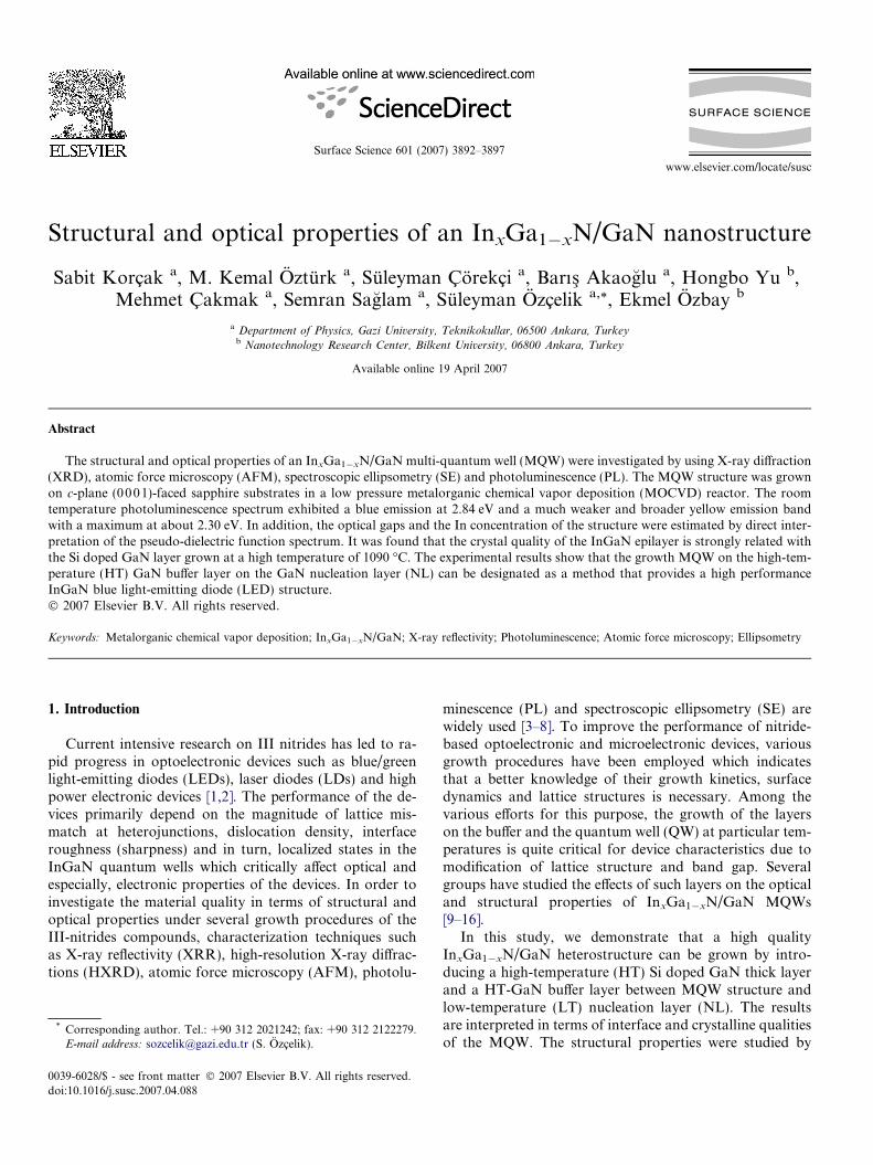
The InxGa1�xN MQW was grown by MOCVD on a c-plane (0001)-faced sapphire substrate with a 100 nm-thickLT-GaN nucleation layer. During the growth, the reactorpressure was maintained at 200mbar. Prior to the growthof MQW, a HT-GaN buffer layer with a thickness of700 nm was deposited at 1050 �C and then a n-type GaN:Silayer of thickness 250 nm was grown at 1090 �C. The sam-ple contains five periods of 4-nm InxGa1�xN active layerthat is grown on a thin 16-nm GaN grown at 710 �C.The cap layer was capped with a 200-nm-thick p-typeGaN:Mg grown at 1030 �C. Fig. 1a shows the schemati-cally drawing of the above mentioned structure and the tar-get values of the thickness are presented in the brackets.
The XRD and reciprocal space mapping (RSM) mea-surement were performed using a D8/Bruker diffractome-ter, equipped on the primary side with a Ge(02 2)monochromator. Surface morphology was observed byAFM using an Omicron VT (variable temperature) STM/AFM instrument at room temperature and atmospherepressure. SE measurements were performed by an UVISELvariable angle spectroscopic phase modulated ellipsometer(Jobin Yvon-Horiba) with a spectral range 0.59–4.7 eV.The orientations of the analyzer and modulator were setto 45� and 0�, respectively. In this configuration, the systemmeasures Is = sin(2w)sin(D) and Ic = sin(2w)cos(D) where wand D are conventional ellipsometric angles [17]. 55 mWHe–Cd laser (325 nm) is used as a light source in room tem-perature PL measurements.
Fig. 1. (a) The schematic representation and structural properties of the MQW(b) The reflectivity of the 5· MQW sample. Arrows point the satellite peaks.
3. Results and discussion
The MQW structure is presented with the measuredstructural properties by HXRD in Fig. 1a. When a GaNepilayer is desired to be grown on sapphire substrates, itis necessary to grow a thin GaN NL at low temperatureof about 500 �C due to a large lattice-mismatch up to13.6% between GaN and sapphire. Then, the growth tem-perature is subsequently raised to more than about1050 �C to grow a thick GaN buffer layer prior to thegrowth of any device structure. During the subsequenthigh-temperature (HT) growth, the HT islands are initiallyexpected to be formed, and then laterally coalescence oc-curs which finally leads to an atomically flat surface [18].
X-ray reflectivity scan for the azimuth orientation of thesample was performed using Cu (1.54 A) radiation asshown in Fig. 1b. In principle, the thicknesses of the layers,their chemical composition as well as the root mean square(rms) roughness of the interfaces can be obtained fromsuch measurements. As shown in the Fig. 1b, the plateauregion in the about 0–0.7� interval is strongly smoothwhich suggests that the sample surface is uniform. Themeasured reflection curve exhibits an exponential behaviorand gives the satellite peaks up to SL + 5th order. In thereflectivity curve, no clear satellite (SL) peaks were ob-served because the height of the satellite is strongly influ-enced by the interface roughness, and by the thickness ofthe individual layers building up the multilayer period.There is a strong contribution of a background that alsodepends on the sample orientation. After subtracting a dif-fuse background, the period D of the stack is determined tobe D = dwell + dbarrier = (17.9 ± 0.5) nm with r = dwell +dbarrier = (1.6 ± 0.1) nm rms roughness. Relatively higherdegree of roughness affects the satellite oscillation in thereflectivity curve and particularly, its amplitude decreases.
structure. Values within the bracket show the nominal values of the layers.
2θ−axis (degree)33 34 35 36 37 38
Inte
nsi
ty (
arb
. un
its)
Experimental CuKα1 (1.54Å)Simulation
(0004)
SL+1
SL+3
SL-1
SL-2
SL-3
SL-0
SL+2SL-4SL-5
GaN
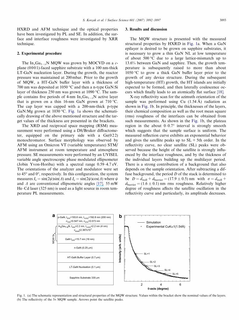
Fig. 2. The 2h-axis scan for the (004) reflection of the 5· MQW sample.
3894 S. Korcak et al. / Surface Science 601 (2007) 3892–3897
Reflectivity measurements were simulated by the LEPTOSprogram [19], which is supported by the simulated anneal-ing method.
In Fig. 2, we present the x–2h scan curve for the sym-metrical (00 4) Bragg reflection along the (110) azimuth.In this figure, the simulation of an HXRD scan using the
Theta (degree)16.8 17.0 17.2 17.4 17.6 17.8
Inte
nsi
ty (
x10
4)(
cps)
0
20
40
60
80
100
120
140
160
180
200
GaN(002)
qx(x10-2)-8 -6 -4 -2
qz
(1/n
m)
7.50
7.55
7.60
7.65
7.70
7.75
7.80
7.85
GaN(004)
ω=θ
a
c
Fig. 3. (a,b) XRD rocking curves of the GaN film used the in (002) and (10MQW sample on GaN/c-sapphire. The x = h line corresponds to the scan in
LEPTOS program that is based on the solution of theTakagi–Taupin equations of the dynamical diffraction the-ory is also shown [20]. High order satellites up to SL + 3thand SL � 5th orders can be clearly distinguished, whichindicate very good InGaN/GaN interfaces. The GaN peaklocalized at an angle of 36.410� is very sharp, whereas allthe satellite bands are narrow. Finer structures are seen be-tween the satellite peaks. This indicates quite good crystal-linity [16]. However, the fringes between satellites are notclearly resolved. Therefore, no information about the layerroughnesses is obtained. Also normal lattice mismatch ra-tio perpendicular to the sample surface is found to be2.367 · 10�3 by using GaN and InN lattice parameters.Using the LEPTOS program, the well width, barrier widthand indium composition were estimated to be approxi-mately as 2.2 nm, 15.7 nm and 9.6%, respectively.
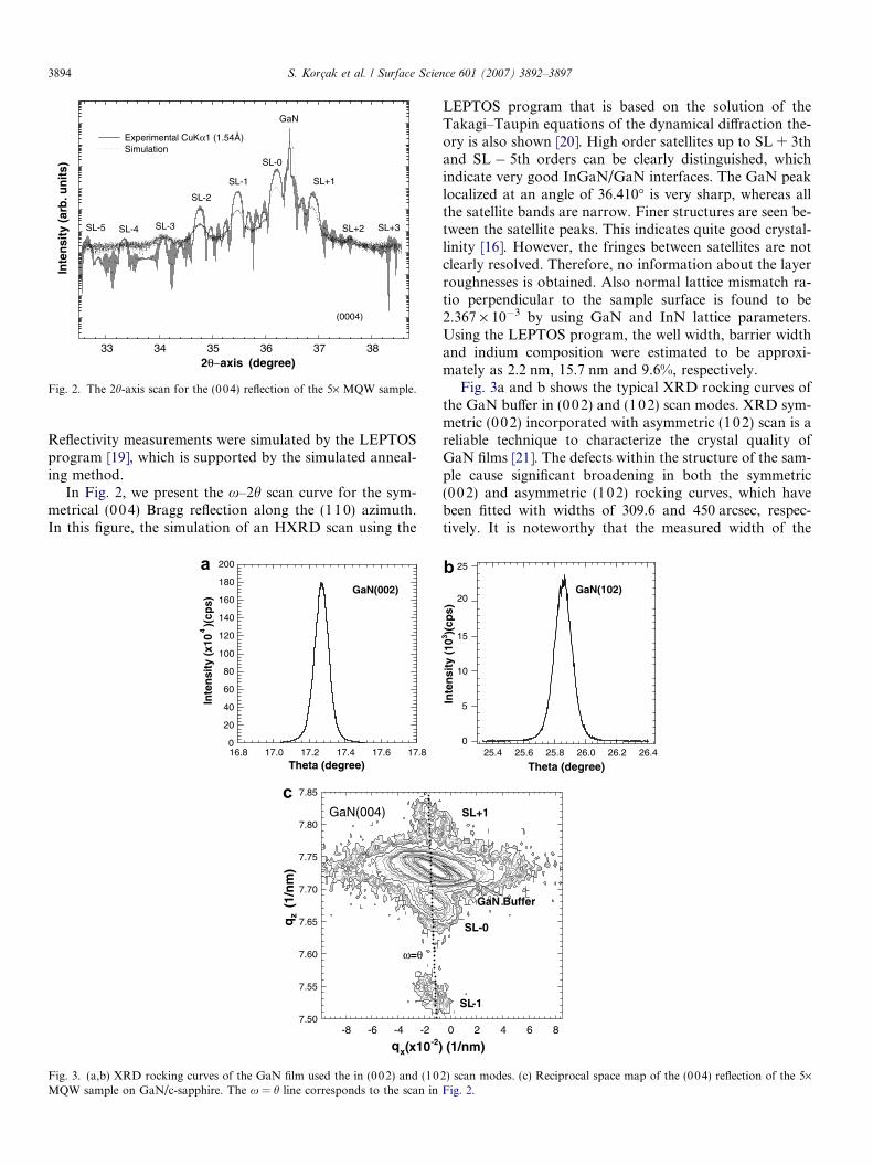
Fig. 3a and b shows the typical XRD rocking curves ofthe GaN buffer in (002) and (102) scan modes. XRD sym-metric (002) incorporated with asymmetric (102) scan is areliable technique to characterize the crystal quality ofGaN films [21]. The defects within the structure of the sam-ple cause significant broadening in both the symmetric(00 2) and asymmetric (10 2) rocking curves, which havebeen fitted with widths of 309.6 and 450 arcsec, respec-tively. It is noteworthy that the measured width of the
Theta (degree)25.4 25.6 25.8 26.0 26.2 26.4
Inte
nsi
ty (
103 )(
cps)
0
5
10
15
20
25
GaN(102)
(1/nm) 0 2 4 6 8
GaN Buffer
SL-0
SL-1
SL+1
b
2) scan modes. (c) Reciprocal space map of the (004) reflection of the 5·Fig. 2.
S. Korcak et al. / Surface Science 601 (2007) 3892–3897 3895
(102) rocking curve is larger than that of the (002) rockingcurve. The broadening of the asymmetric diffractions com-pared to the symmetric diffractions is indicative of a defec-tive structure with a large pure edge threading dislocation(TD) content, since the (002) peak is only broadened byscrew or mixed TD while the (102) peak is broadened byall of the TDs. It is very likely that the high-density edge-type TDs compensate the background of GaN for our sam-ple, leading to the semi-insulating electrical character [22].
The reciprocal map for a (002) diffraction of the (In,Ga)N quantum well structure is shown in Fig. 3c. Theintensity maxima of the GaN buffer layer and the MQWsystem is set along the line x = h, indicating that theMQW is uniform with respect to the GaN buffer layer. Thisresult is in consistent with the XRR and HXRD results.Along the x–2h-direction (q?-direction), strain variationand thickness fluctuations of the SL can be seen clearlyalong the growth direction in the figure. In the x-direction(qk), it is apparent that the structure peaks exhibit somespreading mosaic pattern with an area of which consider-ably increases for the higher SL.
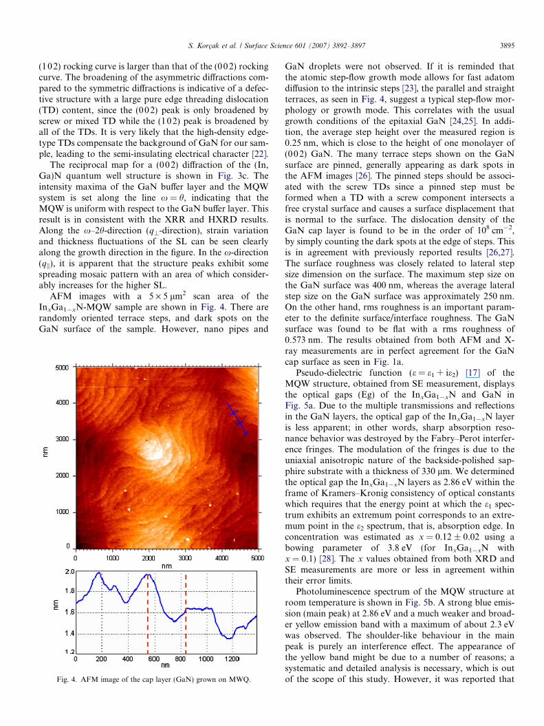
AFM images with a 5 · 5 lm2 scan area of theInxGa1�xN-MQW sample are shown in Fig. 4. There arerandomly oriented terrace steps, and dark spots on theGaN surface of the sample. However, nano pipes and
Fig. 4. AFM image of the cap layer (GaN) grown on MWQ.
GaN droplets were not observed. If it is reminded thatthe atomic step-flow growth mode allows for fast adatomdiffusion to the intrinsic steps [23], the parallel and straightterraces, as seen in Fig. 4, suggest a typical step-flow mor-phology or growth mode. This correlates with the usualgrowth conditions of the epitaxial GaN [24,25]. In addi-tion, the average step height over the measured region is0.25 nm, which is close to the height of one monolayer of(002) GaN. The many terrace steps shown on the GaNsurface are pinned, generally appearing as dark spots inthe AFM images [26]. The pinned steps should be associ-ated with the screw TDs since a pinned step must beformed when a TD with a screw component intersects afree crystal surface and causes a surface displacement thatis normal to the surface. The dislocation density of theGaN cap layer is found to be in the order of 108 cm�2,by simply counting the dark spots at the edge of steps. Thisis in agreement with previously reported results [26,27].The surface roughness was closely related to lateral stepsize dimension on the surface. The maximum step size onthe GaN surface was 400 nm, whereas the average lateralstep size on the GaN surface was approximately 250 nm.On the other hand, rms roughness is an important param-eter to the definite surface/interface roughness. The GaNsurface was found to be flat with a rms roughness of0.573 nm. The results obtained from both AFM and X-ray measurements are in perfect agreement for the GaNcap surface as seen in Fig. 1a.
Pseudo-dielectric function (e = e1 + ie2) [17] of theMQW structure, obtained from SE measurement, displaysthe optical gaps (Eg) of the InxGa1�xN and GaN inFig. 5a. Due to the multiple transmissions and reflectionsin the GaN layers, the optical gap of the InxGa1�xN layeris less apparent; in other words, sharp absorption reso-nance behavior was destroyed by the Fabry–Perot interfer-ence fringes. The modulation of the fringes is due to theuniaxial anisotropic nature of the backside-polished sap-phire substrate with a thickness of 330 lm. We determinedthe optical gap the InxGa1�xN layers as 2.86 eV within theframe of Kramers–Kronig consistency of optical constantswhich requires that the energy point at which the e1 spec-trum exhibits an extremum point corresponds to an extre-mum point in the e2 spectrum, that is, absorption edge. Inconcentration was estimated as x = 0.12 ± 0.02 using abowing parameter of 3.8 eV (for InxGa1�xN withx = 0.1) [28]. The x values obtained from both XRD andSE measurements are more or less in agreement withintheir error limits.
Photoluminescence spectrum of the MQW structure atroom temperature is shown in Fig. 5b. A strong blue emis-sion (main peak) at 2.86 eV and a much weaker and broad-er yellow emission band with a maximum of about 2.3 eVwas observed. The shoulder-like behaviour in the mainpeak is purely an interference effect. The appearance ofthe yellow band might be due to a number of reasons; asystematic and detailed analysis is necessary, which is outof the scope of this study. However, it was reported that
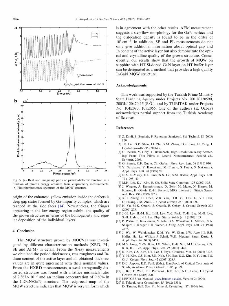
Fig. 5. (a) Real and imaginary parts of pseudo-dielectric function as afunction of photon energy obtained from ellipsometry measurements.(b) Photoluminescence spectrum of the MQW structure.
3896 S. Korcak et al. / Surface Science 601 (2007) 3892–3897
origin of the enhanced yellow emission inside the defects isdeep gap states formed by Ga-impurity complex, which aretrapped at the side faces [14]. Nevertheless, the fringesappearing in the low energy region exhibit the quality ofthe grown structure in terms of the homogeneity and regu-lar deposition of the individual layers.
4. Conclusion
The MQW structure grown by MOCVD was investi-gated by different characterization methods (XRD, PL,SE and AFM) in detail. From the X-ray measurementswe obtained the period thicknesses, rms roughness and In-dium content of the active layer and all obtained thicknessvalues are in quite agreement with their nominal values.From the HXRD measurements, a weak tetragonally dis-torted structure was found with a lattice mismatch ratioof 2.367 · 10�3 and an indium concentration of 9.60% inthe InGaN/GaN structure. The reciprocal map of theMQW structure indicates that MQW is very uniform which
is in agreement with the other results. AFM measurementsuggests a step-flow morphology for the GaN surface andthe dislocation density is found to be in the order of108 cm�2. In addition, SE and PL measurements do notonly give additional information about optical gap andIn content of the active layer but also demonstrate the opti-cal and crystalline quality of the grown structure. Conse-quently, our results show that the growth of MQW onsapphire with HT Si-doped GaN layer on HT buffer layercan be designated as a method that provides a high qualityInGaN MQW structure.
Acknowledgements
This work was supported by the Turkish Prime MinistryState Planning Agency under Projects No. 2001K120590,2003K120470-15 (S.O.), and by TUBITAK under ProjectsNo. 104E090, 105E066. One of the authors (E. Ozbay)acknowledges partial support from the Turkish Academyof Sciences.
References
[1] Z. Dridi, B. Bouhafs, P. Ruterana, Semicond. Sci. Technol. 18 (2003)850.
[2] J.P. Liu, G.D. Shen, J.J. Zhu, S.M. Zhang, D.S. Jiang, H. Yang, J.Crystal Growth 295 (2006) 7.
[3] U. Pietsch, V. Holy, T. Baumbach, High-Resolution X-ray Scatter-ing: From Thin Films to Lateral Nanostructures, Second ed.,Springer, 2004.
[4] G. Binnig, C.F. Quate, Ch. Gerber, Phys. Rev. Lett. 56 (1986) 930.[5] Y. Narukawa, Y. Kawakami, M. Funato, S. Fujita, S. Nakamura,
Appl. Phys. Lett. 70 (1997) 981.[6] N.A. El-Masry, E.L. Piner, S.X. Liu, S.M. Bedair, Appl. Phys. Lett.
72 (1998) 40.[7] M.H. Lee, K.J. Kim, E. Oh, Solid State Commun. 123 (2002) 395.[8] J. Wagner, A. Ramakrishnan, D. Behr, M. Maier, N. Herres, M.
Kunzer, H. Obloh, K.-H. Bachem, MRS Internet J. Nitride Semic-ond. Res. 4S1 (1999) G2.8.
[9] X.H. Zheng, H. Chen, Z.B. Yan, H.B. Yu, D.S. Li, Y.J. Han,Q. Huang, J.M. Zhou, J. Crystal Growth 257 (2003) 326.
[10] H. Yu, M.K. Ozturk, S. Ozcelik, E. Ozbay, J. Crystal Growth 293(2006) 273.
[11] J.-H. Lee, H.-M. Ko, I.-H. Lee, Y.-J. Park, Y.-H. Lee, M.-B. Lee,S.-H. Hahm, J.-H. Lee, Phys. Status Solidi (c) 1 (2002) 103.
[12] P. Perlin, C. Kisielowski, V. Iota, B.A. Weinstein, L. Mattos, N.A.Shapiro, J. Kruger, E.R. Weber, J. Yang, Appl. Phys. Lett. 73 (1998)2778.
[13] J. Wu, W. Walukiewicz, K.M. Yu, W. Shan, J.W. Ager III, E.E.Haller, Hai Lu, William J. Schaff, W.K. Metzger, Sarah Kurtz, J.Appl. Phys. 94 (2003) 6478.
[14] M.S. Jeong, Y.-W. Kim, J.O. White, E.-K. Suh, M.G. Cheong, C.S.Kim, H.J. Lee, Appl. Phys. Lett. 79 (2001) 3440.
[15] K. Kim, C.S. Kim, J.Y. Lee, J. Phys.: Condens. Mat. 18 (2006) 3127.[16] Y.-H. Kim, C.S. Kim, S.K. Noh, S.K. Ban, S.G. Kim, K.Y. Lim, B.S.
O, J. Korean Phys. Soc. 42 (2003) S285.[17] D.E. Aspnes, E.D. Palik (Eds.), Handbook of Optical Constants of
Solids, Academic Press, Orlando, 1985, p. 89.[18] J. Bai, T. Wan, P.J. Parbrook, K.B. Lee, A.G. Cullis, J. Crystal
Growth 282 (2005) 290.[19] LEPTOS User Manual (www.bruker-axs.de), Version 2 (2004).[20] S. Takaqi, Acta Crystallogr. 15 (1962) 1311;
D. Taupin, Bull. Soc. Fr. Mineral. Crystallogr. 87 (1964) 469.

S. Korcak et al. / Surface Science 601 (2007) 3892–3897 3897
[21] B. Heying, X.H. Wu, S. Keller, Y. Li, D. Kapolnek, B.P. Keller, S.P.DenBaars, J.S. Speck, Appl. Phys. Lett. 68 (1996) 643.
[22] H. Yu, D. Caliskan, E. Ozbay, J. Appl. Phys. 100 (2006) 033501.[23] G.B. Stephenson, J.A. Eastman, C. Thompson, O. Auciello, L.J.
Thompson, A. Munkholm, P. Fini, S.P. DenBaars, J.S. Speck, Appl.Phys. Lett. 74 (1999) 3326.
[24] A. Jimenez, Z. Bougrioua, J.M. Tirado, A. Brana, F. Calleja, E.E.Munoz, I. Moerman, Appl. Phys. Lett. 82 (2003) 4827.
[25] A. Torabi, P. Ericson, E.J. Yarranton, W.E. Hooke, J. Vac. Sci.Technol. B 20 (3) (2002) 1234.
[26] J. Bai, T. Wang, P. Comming, P.J. Parbrook, J.P.R. David, A.G.Cullis, J. Appl. Phys. 99 (2006) 023513.
[27] T. Aggerstam, S. Lourdudoss, H.H. Radamson, M. Sjodin, P.Lorenzini, D.C. Look, Thin Solid Films 515 (2006) 705.
[28] C.G. Van de Walle, M.D. McCluskey, C.P. Master, L.T. Romano,N.M. Johnson, Mater. Sci. Eng. B59 (1999) 274.


![Excitonic properties of strained wurtzite and zinc-blende GaN/Al[sub x]Ga[sub 1−x]N quantum dots](https://img.pdfslide.net/doc/110x75/634eb5cd3bdc8e88100807fa/excitonic-properties-of-strained-wurtzite-and-zinc-blende-ganalsub-xgasub-1xn.jpg)


