Embed Size (px)
Citation preview

SHUKLA ET AL. VOL. 5 ’ NO. 3 ’ 1947–1957 ’ 2011 1947
www.acsnano.org
March 02, 2011
C 2011 American Chemical Society
Subwavelength Direct Laser Patterningof Conductive Gold Nanostructures bySimultaneous Photopolymerizationand PhotoreductionShobha Shukla,†,^ Xavier Vidal,^ Edward P. Furlani,^ Mark T. Swihart,§,^ Kyoung-Tae Kim,† Yong-Kyu Yoon,†
Augustine Urbas, ) and Paras N. Prasad†,‡,^,*
†Department of Electrical Engineering, ‡Department of Chemistry, §Department of Chemical and Biological Engineering, and ^Institute for Lasers, Photonics andBiophotonics, University at Buffalo, State University of New York, Buffalo, New York 14260, United States, and )Air Force Research Laboratory, Wright-PattersonAir Force Base, Ohio 45433, United States
Fabrication of metallic nanostructureswithin a dielectric host material allowsthe optical response of the composite
material to be tailored, potentially achievingresponses not possible in a homogeneousmaterial.1-5 This capability is most notablyexploited in the rapidly advancing field ofoptical metamaterials, a new class of nano-structured materials that exhibit electro-magnetic properties, such as a negativerefractive index, that are not observed innaturally occurringmaterials.3,6-9 Theuniqueproperties of metamaterials arise from theengineered electromagnetic response of theconstituent metallic nanostructures. Meta-materials hold promise for numerous appli-cations such as far-field subwavelengthimaging, invisibility cloaking, nanoscale opti-cal trapping, ultracompact waveguides, andoptical power limiting.9-11 Most experimen-tally realized negative index metamaterialshave been fabricated using “top-down” litho-graphic techniques, usually either electron-beam lithography (EBL) or focused-ion-beamlithography (FIBL).1,3,8,12,13 Although theseapproaches can provide resolution on thescaleofa fewnanometers, theyare inherentlyserial in nature and are limited to the fabrica-tion of relatively small samples, typically withhigh-cost and low-throughput. Amore recentapproach to metamaterials involves directlaserwriting in apolymeric structure followedby metal evaporation over the fabricatedsurface.3 While this method is promising, fullmetal coverage is challenging. A need existsfor new fabrication methods that overcomethe aforementioned limitations.In this paper we discuss, demonstrate,
and analyze a novel bottom-up approach
for the fabrication of conductive metalnano- and microstructures that is based on
two-photon absorption-induced photo-
chemistry.14 This approach can significantly
simplify the fabrication of metallic nanos-
tructures in a polymeric host and can po-
tentially enable fabrication of true three-
dimensional metamaterials with low-cost
and high-throughput. Although earlier
studies have demonstrated the use of two-
photon lithography to fabricate metallic
micro- and nanostructures, most of this
work has involved silver nanostructures,
and very few prior studies investigated the
use of gold.15,16 The ability to write gold
nanostructures in a polymeric host is not
only useful for metamaterials but also has
broader potential to enable disruptive ad-
vances in emerging fields such as flexible
*Address correspondence [email protected].
Received for review November 7, 2010and accepted January 25, 2011.
Published online10.1021/nn103015g
ABSTRACT This article presents a new method for fabricating highly conductive gold
nanostructures within a polymeric matrix with subwavelength resolution. The nanostructures are
directly written in a gold precursor-doped photoresist using a femtosecond pulsed laser. The laser
energy is absorbed by a two-photon dye, which induces simultaneous reduction of gold in the
precursor and polymerization of the negative photoresist. This results in gold nanoparticle-doped
polymeric lines that exhibit both plasmonic effects, due to the constituent gold nanoparticles, and
relatively high conductivity (within an order of magnitude of the bulk metal), due to the high density
of particles within these lines. Line widths from 150 to 1000 nm have been achieved with this
method. Various optically functional structures have been prepared, and their structural and optical
properties have been characterized. The influence of laser intensity and scan speed on feature size
have been studied and found to be in agreement with predictions of a mathematical model of the
process.
KEYWORDS: nanocomposites . two-photon lithography . metamaterials . goldnanostructures . nanofabrication
ARTIC
LE

SHUKLA ET AL. VOL. 5 ’ NO. 3 ’ 1947–1957 ’ 2011 1948
www.acsnano.org
electronics, nanophotonics, and plasmonics.3,17-22
Metallic structures can be directly written using thephotoreduction of metal ions. Tanaka et al.16 demon-strated the production of silver microstructures in anaqueous solution, but the reduced silver structures hadnon-uniform density due to diffusion and mixingeffects that are driven by the femtosecond pulsedirradiation in the liquid. Baldacchini et al.23 appliedphotoreduction of silver nitrate in a thin polymer(polyvinylpyrrolidone) film to produce metallic silver,and Maruo and Saeki24 have adapted this process towrite structures. However, this produced relatively low-quality metal structures due to discontinuities be-tween aggregated nanoparticles. As noted above,there have been few reports on two-photon-assistedin situ photoreduction of gold ions.15,16 Moreover, themethods reported so far not only suffer from diffusionand aggregation problems but also have been unableto achieve submicrometer feature sizes due to localheating during the writing process.The two-photon-initiated direct laser writing meth-
od demonstrated and analyzed here is well-suited forthe fabrication of micro- and nanoscale features be-cause it is based on the initiation of a photochemicalprocess within a small (subwavelength) focal volumethat is limited in all three spatial dimensions.1,14,25,26
Furthermore, simultaneous metal reduction and pho-topolymerization reduces diffusion-related broaden-ing of features and nanoparticle aggregation becausethe matrix surrounding newly formed gold nanoparti-cles is cross-linked at the same time that the particlesare formed. Thus, the metallic structures are simulta-neously formed and immobilized. We demonstratethe use of this process for producing uniform goldnanoparticles within continuous gold nanoparticle-doped polymeric structures with line widths of 150 to
1000 nm. We also demonstrate production of opticallyfunctional structures and characterize these with re-spect to their structural, optical, and electrical proper-ties (i.e., conductivity). Our initial study suggests thateven smaller line widths can be achieved using opti-mized combinations of laser and optics.
RESULTS AND DISCUSSION
The writing process is illustrated schematically inFigure 1 and described in greater detail in theMaterialsand Methods section. Typical directly written anddeveloped metallic structures embedded in the poly-mer are shown in Figure 2. The SEM image (Figure 2a)illustrates the topography of the gold/polymer com-posite line, while the backscattered SEM in the lowerright inset more clearly demonstrates the presence ofgold nanoparticles within the polymer, based on thelarge atomic-number-based contrast difference be-tween gold and the polymer. When the distancebetween two fabricated lines was small, some evensmaller “bridging” structures were produced connect-ing the lines. This is similar to the effect observed byTan et al.27 and is attributed to the overlap of the low-intensity portion of the beam between the lines. Linesthus formed are a few hundred nanometers in width.By changing the laser power, we were able to tune thelinewidth from 1 μm to as small as 150 nm, as shown inFigure 2b. SEM imaging of structures written at lowlaser power confirmed the production of polymericlines as narrow as 150 nm, with gold nanoparticles(e50 nm diameter) embedded within them.Cross-linked polymer lines containing gold nanopar-
ticles can only be formed in the laser-exposed regionswhere the amount of photoacid generated is sufficientto both initiate polymerization of the SU8 monomerand reduce enough of the gold precursor to induce
Figure 1. Schematic of the experimental setup.
ARTIC
LE

SHUKLA ET AL. VOL. 5 ’ NO. 3 ’ 1947–1957 ’ 2011 1949
www.acsnano.org
particle nucleation. Normally, additional photoinitiatordecomposition can occur by a free-radical driven cycle(vide infra). However, the gold precursor appears tocompetewith these reactions, decreasing the extent ofphotoinitiator decomposition. Thus, a relatively largeamount of photoacid generator is required in thisprocess. At low writing power (Figure 2b), the goldnanoparticles are concentrated near the center of theline, where the laser intensity is highest, while at anincreased power of 50 mW, gold nanoparticles could befound throughout the fabricated structure (Figure 2a).As laser intensity increases, for a given exposure time,the width of the gold nanoparticle-rich region increasesmore than the width of the polymer line, showing thatthe photoreduction and photopolymerization havedifferent threshold photon doses. Extinction spectrashow a broad band centered at 570 nm (Figure 2c) thatis attributed to excitation of localized surface plasmonresonances (LSPR) of the gold nanoparticles and that isnot present in the unexposed film. Extinction spectrawere recorded using a halogen lamp as a white lightsource and subtracting absorbance of the bare glassslide. The LSPR peak of gold nanoparticles can appearfrom 525 to 600 nm, depending on the size and shapeof the nanoparticles and the coupling between them.In this sample, we have a distribution of nanoparticlesizes, and the particles are sufficiently close to one
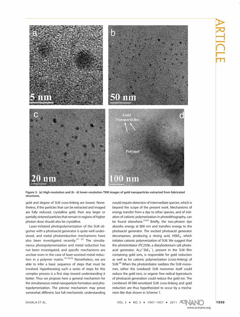
another to achieve overall conductivity. This broadensand red shifts the LSPR peak relative to that expectedfor small, monodispersed particles suspended in a solvent.Energy-dispersive X-ray spectroscopy (EDS) was alsoperformed to check the composition of the fabricatedstructures (Figure 2d). The only elements detectedwere gold and the constituents of the glass substrate(e.g., K, Zn, and Ti). The large peak fromSi in the substrateis outside the energy range shown in the inset ofFigure 2d. Notably, no chlorine is detected by EDS.This suggests that all gold in the lines is fully reduced,as one would expect that any ionic gold would beaccompanied by chlorine counterions. For TEM imag-ing of gold nanoparticles produced within the poly-meric matrix, the gold nanostructures were suspendedin ethanol by scratching the fabricated polymeric goldcomposite structure with a diamond cutter tip andsonicating for 30 min. It is evident from TEM images,such as those shown in Figure 3, that the extractedgold nanoparticles are not aggregated and are highlycrystalline. Figure 3a shows the crystallinity of indivi-dual nanoparticles, while Figure 3b-d shows goldnanoparticles still embedded in polymer. Of course,the sample of gold particles imaged in TEM is biasedtoward those that could be extracted from the filmalong with residual polymer. Perhaps these are parti-cles near the edge of a line where both the density of
Figure 2. (a) Secondary electron emission image of the gold nanoparticle-doped polymeric structure produced at 50 mWlaser powerby two-photon-initiatedphotoreduction/polymerization (top inset, bridging structures formedwhen the spacingbetween the two lines was 4 μm; bottom inset, backscattered image showing gold nanoparticles). (b) Secondary emissionSEM image of the structure fabricated at 20mW laser power (inset: backscattered image). (c) Absorbance spectra of film withembedded gold nanostructures. (d) EDS spectra of the metallic structures.
ARTIC
LE
SHUKLA ET AL. VOL. 5 ’ NO. 3 ’ 1947–1957 ’ 2011 1950
www.acsnano.org
gold and degree of SU8 cross-linking are lowest. None-theless, if the particles that can be extracted and imagedare fully reduced, crystalline gold, then any larger orpartially sinteredparticles that remain in regionsofhigherphoton dose should also be crystalline.Laser-initiated photopolymerization of the SU8 oli-
gomer with a photoacid generator is quite well under-stood, and metal photoreduction mechanisms havealso been investigated recently.27-32 The simulta-neous photopolymerization and metal reduction hasnot been investigated, and specific mechanisms areunclear even in the case of laser-assisted metal reduc-tion in a polymer matrix.15,16,33 Nonetheless, we areable to infer a basic sequence of steps that must beinvolved. Hypothesizing such a series of steps for thiscomplex process is a first step toward understanding itbetter. Thus we propose here a general mechanism forthe simultaneousmetal nanoparticle formation and pho-topolymerization. The precise mechanism may provesomewhat different, but full mechanistic understanding
would require detection of intermediate species, which isbeyond the scope of the present work. Mechanisms ofenergy transfer from a dye to other species, and of initi-ation of cationic polymerization in photolithography, canbe found elsewhere.13,24 Briefly, the two-photon dyeabsorbs energy at 800 nm and transfers energy to thephotoacid generator. The excited photoacid generatordecomposes, producing a strong acid, HSbF6, whichinitiates cationic polymerization of SU8. We suggest thatthe photoinitiator (PC2506, a diaryliodonium salt photo-acid generator, Ar2I
þSbF6-), present in the SU8 film
containing gold ions, is responsible for gold reductionas well as for cationic polymerization (cross-linking) ofSU8.29 When the photoinitiator oxidizes the SU8 mono-mer, either the (oxidized) SU8 monomer itself couldreduce the gold ions, or organic free radical byproductsof photoacid generation could reduce the gold ion. Thecombined AF380-sensitized SU8 cross-linking and goldreduction are thus hypothesized to occur by a mecha-nism like that shown in Scheme 1.
Figure 3. (a) High-resolution and (b-d) lower-resolution TEM images of gold nanoparticles extracted from fabricatedstructures.
ARTIC
LE

SHUKLA ET AL. VOL. 5 ’ NO. 3 ’ 1947–1957 ’ 2011 1951
www.acsnano.org
When photoacid, HSbF6, is produced from thephotoinitiator, aryl radicals and other radicals areproduced as byproducts (Scheme 1, steps 3 and 4).30
These can abstract hydrogen from the monomer orpolymer to produce radicals by processes like thatshown in step 7. In the absence of gold precursors,these radicals can react with the photoinitiator (step 8),leading to the cycle of free-radical-induced initiatordecomposition shown in steps 7, 8, and 9 ofScheme 1.30 In the presence of gold precursor, theradicals generated in step 7 may instead reduce thegold precursor as shown in step 10. The resultingAuCl3
- contains gold in the unstable Au2þ oxidationstate. This undergoes disproportionation reactions likethose illustrated in steps 11 and 12, ultimately produ-cing one fully reduced Au0 atom for every three AuCl3
-
ions generated by step 10 and regenerating twoprecursor ions (AuCl4
-).34-37 The Au0 atoms are ex-pected to form gold nanoparticles by diffusion-limitedaggregation. However, as they are produced, their
mobility is also decreasing due to simultaneouscross-linking of SU8 in which they are formed. Ofcourse, many minor variations of the above mecha-nism are conceivable, but a sequence of events likethose listed here is consistent with the observedbehavior of simultaneous photopolymerization andgold reduction and with known mechanisms of pho-topolymerization and gold reduction alone.We have studied the effects of laser power and total
photon dose on feature size by varying the scanningspeed (Figure 4a) and the laser power. We were notable to use SEM imaging to compare line widthswritten at extremely low power, as these were easilywashed off from the substrate during sample devel-opment. SEM imaging requires removal of the un-exposed photoresist within which the lines are em-bedded. However, without the film for support, narrowlines often did not adhere to the substrate. Figure 2bshows a case where the polymerized line has remainedon the substrate. However, in most other cases, the
Scheme 1. Proposed mechanism of simultaneous photoreduction and photopolymerization.
ARTIC
LE

SHUKLA ET AL. VOL. 5 ’ NO. 3 ’ 1947–1957 ’ 2011 1952
www.acsnano.org
lines were simply washed away, and a systematic studyof the line width by SEM was not practical. Thus, forresults shown in Figures 4 and 5, line widths weremeasured from confocal transmission images. Withthis approach, the apparent line width reflects boththe writing resolution and the imaging resolution. Thismeans that the apparent constant line width at lowlaser power may, in fact, reflect limitations of the linewidth measurement, which might be different forgold-containing lines versus gold-free lines becauseof the higher contrast between gold-containing linesand the surrounding matrix. In confocal fluorescenceimaging, structures written at slower scan speedsshowed brighter fluorescence but did not appear tobe wider than those written at faster scan speeds(Figure 4a). However, this scan speed variation wasonly done with a relatively low power (∼10 mW); athigher power, slow scan speeds led to ablation of thefilm. Formation of more pronounced features of thesame apparent size at slower scan speeds could resultfrom both a greater extent of gold reduction(producing more metallic gold which may increasedye emission via plasmonic field enhancement) anda higher degree of cross-linking (which would better
trap the dye during postexposure washing). However,no detailed explanation can be confirmed at this time.In addition, we studied the influence of the goldprecursor on the width of the feature size (Figure 4b).The minimum power required for producing a detect-able polymeric feature, 10-15 mW, did not differappreciably between SU8 alone and with the goldprecursor added, but at higher power, this differencewas more significant. The apparent width of the struc-ture written at low power was ∼750 nm for the gold-doped polymer sample and about 1000 nm for theundoped SU8. Confocal fluorescence images of thegold-doped polymer and undoped polymer at 40 mWare shown in Figure 4b, demonstrating a clear decreasein the apparent line width with the addition of goldprecursor. In both cases, the observed feature widthwas independent of the laser power up to somethreshold value (∼30 mW for polymer alone and ∼50mWwithgoldprecursor). Above that value, the linewidthincreased with increasing laser power, as shown inFigure 5. We attribute the decrease in the line widthand increase in the threshold for growth of line width tocoupling between the photoinitiation of cationic poly-merization and the gold reduction process.
Figure 4. (a) Confocal transmission (left) and fluorescence (right) images of structures produced at scanning speeds of50 μms-1 (top) or 5 μms-1 (bottom) at 10mW. (b) Confocal images of gold precursor-doped polymeric feature and undopedpolymeric feature at the same power (40 mW) and scan speed (50 μm s-1).
Figure 5. Polymerization line width vs laser power: comparison of model with experimental data.
ARTIC
LE

SHUKLA ET AL. VOL. 5 ’ NO. 3 ’ 1947–1957 ’ 2011 1953
www.acsnano.org
We have developed a first-order analytical model topredict the linewidthw for ourwritingprocess. Followingsimilar studies in the literature, we assume that SU8 ispolymerized at positions where the total photoacidgenerated F(x,y,z,t) exceeds a threshold value Fth. Theequation governing the behavior of F is as follows
DFDt
¼ (F0 -F)σ2, effN2 (1)
where σ2,eff = σ2η is the “effective” two-photon crosssection, which is the product of the two-photon ab-sorption coefficient, σ2 (cm4/s), of the dye used tosensitize the writing process (AF380) and the efficiencyη< 1 of the initiation process. This efficiency representsthe probability that excitation of the dye leads toenergy transfer to the photoacid generator and pro-duction of the acid (HSbF6 in this system). To the extentthat the gold precursor (AuCl4
-) can also participate inenergy transfer from the dye and can react with(consume) the acid and free-radical byproducts ofphotoacid decomposition, this efficiency is expectedto decrease with increasing concentration of the goldprecursor. N(x,y,z,t) is the photon flux. The laser outputis defined by thewavelength λ of the incident light, thepulse repetition rate ν, the duration of the laser pulse τLduring each repetition, and an average power P. Weassume thatN has a Gaussian spatial distribution at thefocal plane (z = 0) and thus the photon flux at anobservation point (xobs,yobs) in this plane is
N(x, y, z ¼ 0, t)
¼ N0(t)exp - 2(xb - xobs)
2 þ (yb - yobs)2
r20
" #
(2)
where (xb,yb) is the position of the center of the beam.We further assume that the photon flux is constantN0(t) = N0 during each pulse of duration τL. To deter-mine the polymerized line width, we must account forthe motion of the media during the writing process. Tosimplify the analysis, we choose a reference frame atrest with respect to the media and consider the laserbeam to be moving along the y-axis with a constantvelocity. The position of the center of the beam at timet is (xb = 0, yb = vbt). We evaluate the polymerization atan observation point along the x-axis (xobs,yobs - 0).Note that the beam will be over this point at t = 0 (i.e.,yb = yobs). We analyze an infinite scan line and integrateeq 1 as followsZ Fa
0
dF(F0 -F)
¼ σ2, effντLN20
Z þ¥
-¥exp - 4
x2obs þ (vbt)2
r20
!24
35dt (3)
where Fa is the density of activated photoacid gen-erator. Note that to obtain eq 3 we have used the fact
that the integrand is slowly varying during a laser pulseand that it decays exponentially with distance from theobservation point. We set Fa = Fth and solve eq 3 forxobs to determine the distance 0 < x < xth over whichthe film is polymerized. The polymerized line widthw = 2xth is given by
w ¼ r0 ln
ffiffiffiπ
pσ2, effντLr0N2
0
2vbC
!24
351=2
(4)
where C = ln(F0/(F0 - Fth)). In order to evaluate w werelate photon flux to the average laser power
N0 ¼ 2πr20ντL
TP
pωL(5)
where T is the fraction of light transmitted through theobjective. Finally, this leads to an overall expression forthe line width:
w ¼ r0 lnσ2η
TP
pωL
� �2
π3=2vbντLr30lnF0
F0 -Fth
!0BBBBB@
1CCCCCA
2666664
3777775
1=2
(6)
All of the quantities in this expression are known orare readily measurable in separate experiments exceptfor Fth and η. These can be fit to line width data. If thethreshold photoacid concentration Fth is much smallerthan the initial concentration F0, then
C ¼ lnF0
F0 -Fth
!
¼ FthF0
þ 12
FthF0
!2
þ 13
FthF0
!3
þ ::: � FthF0
(7)
In this case, the expression for line width reduces to
w ¼ r0 lnσ2
ηF0Fth
� �TP
pωL
� �2
π3=2vbντLr30
0BBBB@
1CCCCA
266664
3777751=2
(8)
Under these conditions, the effects of Fth and η onthe line width are indistinguishable. The effects couldonly be separated in experiments where the initialphotoacid generator concentration, F0, is not dramati-cally larger than the threshold photoacid concentra-tion, Fth.We apply eq 8 to our experimental results andmodel
line width w as a function of laser power P for the two-photon-induced polymerization process, with andwithout the presence of the gold precursor. Resultsare shown in Figure 5. Our known experimental param-eters are as follows: λ = 800 nm, vb = 50 μm s-1, τL =120 fs, and ν = 76 MHz. The two-photon absorptioncross section of the AF380 dye is σ2 = 3� 10-49 cm4
3 s.We fit eq 8 to our measured data, as shown in Figure 5,
ARTIC
LE
SHUKLA ET AL. VOL. 5 ’ NO. 3 ’ 1947–1957 ’ 2011 1954
www.acsnano.org
using the following parameters: r0 = 940 nm, T = 30%,and ηF0/Fth = 0.0028 and 0.01 for polymerization withandwithout the gold precursor, respectively. The lowerpolymerization efficiency η in the presence of the gold
precursor is due to the fact that it consumes productsof photoacid decomposition, reducing the amountavailable for initiating cationic polymerization of SU8.These fits used only the data in the regime where line
Figure 6. SEM image of (a) nanocauliflower; (b) nanoblocks (insets in a and b show the close-up view of the single element);(c) confocal fluorescence image of the SRR grating structure; (d) confocal transmission image of the fishnet structure; variousstructures made with femtosecond laser lithography: (e-g) fishnet structures, (h) plasmonic cauliflower, (i,j) plasmonicdonuts; (k,l) chiral “y” structure.
ARTIC
LE

SHUKLA ET AL. VOL. 5 ’ NO. 3 ’ 1947–1957 ’ 2011 1955
www.acsnano.org
width was observed to change with the laser power,which is where the line widths measured by confocaltransmission microscopy are expected to be accurate.It is worth noting that extrapolating the polymer-onlyfit to a line width of zero gives a minimum laser powerof 15 mW to produce any polymerization. This isconsistent with the observed minimum energy re-quired to produce an observable line. However, thisexperimental minimum energy for writing was notincreased in the presence of gold precursor, in contrastto the prediction of this first-order model in which thegold precursor reduces the efficiency of photoacidgeneration independently of laser power. This sug-gests that the interaction between gold reduction andSU8 polymerization may be more complex than hasbeen accounted for in this simple first-order model.Nonetheless, the model captures the experimentalresults with sufficient accuracy to serve as a usefulguide to experiment. It should be noted that while weeasily achieved subwavelength line width resolutionwith the gold precursor at low power, our opticalsystemwas not optimized tominimize thewriting spotsize. Therefore, a substantially finer writing resolutionshould be possible using the same process andmateri-als with optimized optics and optomechanical compo-nents. As mentioned previously, periodically arrangedmetal nanostructures produce pronounced localizedsurface plasmon resonances, which result in an intenseelectromagnetic field that extends beyond their phy-sical dimensions.1,2,38-42 The nanostructures can sup-port electric and magnetic resonances that give rise toresonant behavior of the effective bulk permittivity and
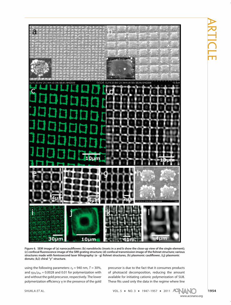
permeability, respectively.43,44 Figure 6a shows anelectronmicrograph of a gold “nano cauliflower” array.The diameter of the gold cauliflower element is 1 μm,and the periodicity is 2 μm. These structures wereprepared using a high gold precursor loading (>30wt %). The exact mechanism governing the formationof the structures is not presently understood and is asubject of our ongoing research. Metal nanoblocksmade at comparatively higher power are shown inFigure 6b. The length to width ratio of these structuresis 2.5 μm/1.5 μm, and the distance between twoelements is approximately 4 μm. Split ring resonator(SRR) structures have also been prepared, as shown inFigure 6c. In these, the spacing between elements was4 μm with an element height of 6 μm. The distancebetween the two ends of the split ring was kept at2 μm. Themost common approach to obtain a practicalnegative-index medium is through incorporation ofnonmagneticmetallic resonators such as the split ringsor various mesh (fishnet) structures. Figure 6d shows agold wire mesh structure with a spacing of 5 μmbetween the neighboring wires. Several other struc-tures prepared by two-photon lithography are shownin Figure 6e-l. In our preliminary report on this meth-od, we also demonstrated production of chiral struc-tures like those in Figure 6k,l, which calculations showcan rotate the polarization of incoming light (also seeSupporting Information S1).10
Last, we characterized the conductivity of the writ-ten lines. This is important because the level of con-ductivity of the fabricated structures will determine therange of utility of the writing process, especially as it
Figure 7. Electrical characterization of gold nanoparticle-doped line structure: (a) geometry of four-point probe measure-ment system; (b) four-point probe system; (c) current vs applied voltage.
ARTIC
LE

SHUKLA ET AL. VOL. 5 ’ NO. 3 ’ 1947–1957 ’ 2011 1956
www.acsnano.org
pertains to applications requiring functional electronicmaterials. We use a four-point probe approach tomeasure conductivity of individual lines, as illustratedin Figure 7a,b. The probe electrodes were deposited onprefabricated written structure on a glass substrate asshown in Figure 7b. The dimensions of the system areshown in Figure 7a. The conductivity measurementwas performed using a digital source meter (Keithley2400). Figure 7c shows the current versus appliedvoltage for a structure that was prepared with 30 wt %gold precursor loading. The fabricated gold lines were800 nm wide and 300 μm long, and their conductivityranged from 1 to 2.5 � 107 mho/m in various repeatedexperiments. Significantly, this is approximately 1/4 thatof bulk gold, which is 4.1 � 107 mho/m. The relativelyhigh conductivity of these structures is due to the highloading fraction of gold precursor and the photoreduc-tion of the precursor into relatively small, denselypacked gold nanoparticles. The ability to write sub-wavelength conductive structures that exhibit plasmo-nic effects is a significant and advantageous feature of
the writing process and holds potential for numerousapplications.
CONCLUSIONS
We have described, demonstrated, and analyzed anew laser-based direct writing method for producingsubwavelength plasmonic and conductive patternedstructures within a polymeric host. The method involvessimultaneous two-photon-initiated photoreduction of agold precursor and polymerization of a negative photo-resist (SU8). Features with line widths as small as 150 nmhave been produced using this approach. Several func-tional structures have been written including opticallyactive planar chiral structures and plasmonic nanostruc-tures, which are used in the development of compositemetamaterials. We have studied various process para-meters and have characterized their impact on theproperties of fabricated structures. We expect this novelapproach of in situ fabrication of plasmonic and conduc-tive structures will enable efficient fabrication of novelthree-dimensional optically functional composite media.
METHODS AND MATERIALSThe experimental arrangement for direct two-photon writing
of gold nanostructures is shown schematically in Figure 1. SU8(Microchem Inc.) served as the matrix within which goldstructures were written by reduction of gold ions from HAuCl4incorporated within the unexposed SU8 film. SU8 includes aphotoacid generator (PC2506, a diaryliodonium salt photoacidgenerator, Ar2I
þSbF6-) as purchased. A two-photon dye, AF380
(provided by the US Air Force Research Laboratory, OH), wasadded to sensitize the mixture to two-photon absorption ofinfrared laser light. Composite films, typically containing 10 wt% gold precursor (HAuCl4 3 3H2O, from Sigma Aldrich) and 1 wt% AF380 in the SU8 photoresist after solvent evaporation, wereproduced by spin-coating on glass coverslips. Cyclopentanonewas used as a solvent for preparing the films because SU8,AF380, and HAuCl4 are all highly soluble in it. The mixture wasvortexed for 15 min and then ultrasonicated for 15 min toensure complete dissolution and mixing.Patterns were written within these films by irradiation with a
mode-locked femtosecond pulsed laser (Ti:sapphire laser withan operating wavelength of 800 nm, a pulse width of <120 fs,and a repetition rate of 76 MHz). The laser light was introducedinto an inverted microscope and focused with an air objectivelens (60�, NA0.85). The laser power was controlled by a gradedneutral density filter. The laser power was measured at theentrance of the microscope; typical power loss from microscopeentrance to the sample was approximately 25%. Unless other-wise indicated, a writing speed of 50 μm per second was used inthe experiments reported here. After writing structures in the film,the unexposed portion could be removed by dipping the film incyclopentanone and then allowing it to air-dry. No post-bakingwas performed; two-photon-initiated photopolymerization of SU8can be done without post-baking because the temperature risedue to laser exposure at the focal region is sufficient to effectivelyanneal the focal volume.45 Samples were studied using a confocalmicroscope (TCS SP2, Leica Microsystems Semiconductor GmbH)with an HXC PL APO CS 63.0 � 1.40 oil immersion objective. Thesamples were illuminated with a pulsed diode laser at 457 nm forfluorescence imaging of the patterned structure using the en-capsulated dye. A photomultiplier tube (PMT) was used fordetection, with a 480-580 nm band-pass filter for fluorescence
and transmission imaging. For linewidth comparisonexperiments,the sample was post-baked for 2 min at 95 �C, developed withPGMEA, and washed with isopropyl alcohol (IPA) to make itphotoinsensitive. With the inclusion of the gold precursor, thecompositefilm cannot be fullywashedwith PGMEAand IPA as thiswill alter the patterned structure. Absorbance spectra of thefabricated structures were recorded with a UV-vis spectropho-tometer (Ocean Optics Inc.). Energy-dispersive X-ray spectroscopyand scanning electronmicroscopywereperformedusing aHitachiS-4000 field-emission SEM.
Acknowledgment. We thank Dr. A Baev and Dr. T YOhulchanskyy for helpful discussion. The support by Air Forceoffice of Scientific Research (Grant No. FA95500910258) andNational Science Foundation (CAREER 0748153) are alsoacknowledged.
Supporting Information Available: S1(a,b) Confocal image ofthe noncentrosymmetric structures: fluorescence and transmis-sion image of (a) the left handed grating structure and (b) theright handed grating structure; (c) analysis of chiral gammadionstructures: rotation of field polarization vs λ in the transmitted;scale bar = 2 μm; (d) computational model for a single elementof a 2D array showing the presence of an Ey field component inthe transmitted field. This material is available free of charge viathe Internet at http://pubs.acs.org.
REFERENCES AND NOTES1. Prasad, P. N. Nanophotonics; John Wiley & Sons: New York,
2004.2. Oldenburg, S. J.; Averitt, R. D.; Westcott, S. L.; Halas, N. J.
Nanoengineering of Optical Resonances. Chem. Phys. Lett.1998, 288, 243–247.
3. Rill, M. S.; Plet, C.; Thiel, M.; Staude, I.; von Freymann, G.;Linden, S.; Wegener, M. Photonic Metamaterials by DirectLaser Writing and Silver Chemical Vapour Deposition. Nat.Mater. 2008, 7, 543–546.
4. Shukla, S.; Kumar, R.; Baev, A.; Gomes, A. S. L.; Prasad, P. N.Control of Spontaneous Emission of CdSe Nanorods in aMultirefringent Triangular Lattice Photonic Crystal. J. Phys.Chem. Lett. 2010, 1, 1437–1441.
ARTIC
LE

SHUKLA ET AL. VOL. 5 ’ NO. 3 ’ 1947–1957 ’ 2011 1957
www.acsnano.org
5. Shukla, S.; Baev, A.; Jee, H.; Hu, R.; Burzynski, R.; Yoon, Y. K.;Prasad, P. N. Large Area near Infrared (IR) Photonic Crystalswith Colloidal Gold Nanoparticles Embedding. ACS Appl.Mater. Interfaces 2010, 2, 1242–1246.
6. Smith, D. R.; Pendry, J. B.;Wiltshire,M. C. K.Metamaterials andNegative Refractive Index. Science 2004, 305, 788–792.
7. Shukla, S.; Kim, K.-T.; Baev, A.; Yoon, Y. K.; Litchinitser, N. M.;Prasad, P. N. Fabrication and Characterization of Gold-Polymer Nanocomposite Plasmonic Nanoarrays in a Por-ous Alumina Template. ACS Nano 2010, 4, 2249–2255.
8. Kuwata-Gonokami, M.; Saito, N.; Ino, Y.; Kauranen, M.;Jefimovs, K.; Vallius, T.; Turunen, J.; Svirko, Y. Giant OpticalActivity in Quasi-Two-Dimensional Planar Nanostructures.Phys. Rev. Lett. 2005, 95, 227401–227404.
9. Furlani, E. P.; Baev, A. Optical Nanotrapping Using CloakingMetamaterial. Phys. Rev. E 2009, 79, 026607–026612.
10. Baev, A.; Furlani, E. P.; Samoc, M.; Prasad, P. N. NegativeRefractivity Assisted Optical Power Limiting. J. Appl. Phys.2007, 102, 043101-5.
11. Furlani, E. P.; Baev, A. Free-Space Excitation of ResonantCavities Formed from Cloaking Metamaterial. J. Mod. Opt.2009, 56, 523–529.
12. Henzie, J.; Lee, J.; Lee, M. H.; Hasan, W.; Odom, T. W.Nanofabrication of Plasmonic Structures. Annu. Rev. Phys.Chem. 2009, 60, 147–165.
13. Lee, K. S.; Kim, R. H.; Yang, D. Y.; Park, S. H. Advances in 3DNano/Microfabrication Using Two-Photon Initiated Po-lymerization. Prog. Polym. Sci. 2008, 33, 631–681.
14. Shukla, S.; Furlani, E. P.; Vidal, X.; Swihart, M. T.; Prasad, P. N.Two-Photon Lithography of Sub-Wavelength MetallicStructures in a Polymer Matrix. Adv. Mater. 2010, 22,3695–3699.
15. Vurth, L.; Baldeck, P.; Stephan, O.; Vitrant, G. Two-PhotonInduced Fabrication of Gold Microstructures in Polysty-rene Sulfonate Thin Films Using a Ruthenium(II) Dye asPhotoinitiator. Appl. Phys. Lett. 2008, 92, 171103-3.
16. Tanaka, T.; Ishikawa, A.; Kawata, S. Two-Photon-InducedReduction of Metal Ions for Fabricating Three-Dimen-sional Electrically Conductive Metallic Microstructure.Appl. Phys. Lett. 2006, 88, 081107-3.
17. Henzie, J.; Lee, M. H.; Odom, T. W. Multiscale Patterning ofPlasmonicMetamaterials.Nat. Nanotechnol.2007, 2, 549–554.
18. Wang, M. C. P.; Gates, B. D. Directed Assembly of Nano-wires. Mater Today 2009, 12, 34–43.
19. Nagpal, P.; Lindquist, N. C.; Oh, S.-H.; Norris, D. J. Ultra-smooth Patterned Metals for Plasmonics and Metamate-rials. Science 2009, 325, 594–597.
20. Wu, Z.; Nelson, R. L.; Haus, J. W.; Zhan, Q. PlasmonicElectro-Optic Modulator Design Using a Resonant MetalGrating. Opt. Lett. 2008, 33, 551–553.
21. Nam, S.; Jiang, X.; Xiong, Q.; Ham, D.; Lieber, C. M. VerticallyIntegrated, Three-Dimensional Nanowire Complemen-taryMetal-Oxide-Semiconductor Circuits. Proc. Natl. Acad.Sci. U.S.A. 2009, 106, 21035–21038.
22. Bratkovsky, A.; Ponizovskaya, E.; Wang, S. Y.; Holmstrom, P.;Thylen, L.; Fu, Y.; Agren, H. A Metal-Wire/Quantum-DotComposite Metamaterial with Negative Epsilon and Com-pensated Optical Loss. Appl. Phys. Lett. 2008, 93, 193106-3.
23. Baldacchini, T.; Pons, A.-C.; Pons, J.; LaFratta, C.; Fourkas, J.;Sun, Y.; Naughton, M. Multiphoton Laser Direct Writing ofTwo-Dimensional Silver Structures. Opt. Express 2005, 13,1275–1280.
24. Maruo, S.; Saeki, T. Femtosecond Laser Direct Writing ofMetallic Microstructures by Photoreduction of Silver Nitratein a Polymer Matrix. Opt. Express 2008, 16, 1174–1179.
25. Guo, R.; Li, Z.; Jiang, Z.; Yuan, D.; Huang, W.; Xia, A. Log-PilePhotonic Crystal Fabricated by Two-Photon Photopoly-merization. J. Opt. A: Pure Appl. Opt. 2005, 7, 396–399.
26. Agren, H. Modeling of Multi-Photon-Induced Photolumi-nescence from Organic Fluorophores and Metal-CoatedSemiconductor Nanoparticles. Int. Symp. Biophotonics,Nanophotonics Metamaterial 2006, 26–26.
27. Tan, D.; Li, Y.; Qi, F.; Yang, H.; Gong, Q.; Dong, X.; Duan, X.Reduction in Feature Size of Two-Photon PolymerizationUsing SCR500. Appl. Phys. Lett. 2007, 90, 071106-3.
28. Kumi, G.; Yanez, C. O.; Belfield, K. D.; Fourkas, J. T. High-SpeedMultiphoton Absorption Polymerization: Fabrication of Mi-crofluidic Channels with Arbitrary Cross-Sections and HighAspect Ratios. Lab Chip 2010, 10, 1057–1060.
29. Cho, J.-D.; Ju, H.-T.; Park, Y.-S.; Hong, J.-W. Kinetics of CationicPhotopolymerizations of UV-Curable Epoxy-Based SU8-Ne-gative Photoresists with and without Silica Nanoparticles.Macromol. Mater. Eng. 2006, 291, 1155–1163.
30. Acosta Ortiz, R.; Cisneros, M. d. L. G.; García, G. A. Synthesisof Novel Highly Reactive Silicone-Epoxy Monomers forCationic Photopolymerizations. Polymer 2005, 46, 10663–10671.
31. Torigoe, K.; Esumi, K. Preparation of Colloidal Gold byPhotoreduction of Tetracyanoaurate(1-)-Cationic Surfac-tant Complexes. Langmuir 1992, 8, 59–63.
32. Eustis, S.; El-Sayed, M. A. Molecular Mechanism of thePhotochemical Generation of Gold Nanoparticles in Ethy-lene Glycol: Support for the Disproportionation Mecha-nism. J. Phys. Chem. B 2006, 110, 14014–14019.
33. Bellec, M.; Royon, A.; Bousquet, B.; Bourhis, K.; Treguer, M.;Cardinal, T.; Richardson, M.; Canioni, L. Beat the DiffractionLimit in 3D Direct Laser Writing in Photosensitive Glass.Opt. Express 2009, 17, 10304–10318.
34. Eustis, S.; El Sayed, M. A. Molecular Mechanism of thePhotochemical Generation of Gold Nanoparticles in Ethy-lene Glycol: Support for the Disproportionation Mechan-ism. J. Phys. Chem. B 2006, 110, 14014–14019.
35. Kubo, S.; Diaz, A.; Tang, Y.; Mayer, T. S.; Khoo, I. C.; Mallouk,T. E. Tunability of the Refractive Index of Gold Nanopar-ticle Dispersions. Nano Lett. 2007, 7, 3418–3423.
36. Koga, H.; Tokunaga, E.; Hidaka, M.; Umemura, Y.; Saito, T.;Isogai, A.; Kitaoka, T. Topochemical Synthesis and Cata-lysis of Metal Nanoparticles Exposed on Crystalline Cellu-lose Nanofibers. Chem. Commun. 2010, 46, 8567–8569.
37. Kawamura, G.; Sato, S.; Muto, H.; Sakai, M.; Lim, P. B.;Watanabe, K.; Inoue, M.; Matsuda, A. AgBr Nanocrystal-Dispersed Silsesquioxane-Titania Hybrid Films for Holo-graphic Materials. Mater. Lett. 2010, 64, 2648–2651.
38. Wang, W.; Summers, C. J.; Wang, Z. L. Large-Scale Hex-agonal-Patterned Growth of Aligned Zno Nanorods forNano-Optoelectronics and Nanosensor Arrays. Nano Lett.2004, 4, 423–426.
39. Chan, Y.-H.; Chen, J.; Wark, S. E.; Skiles, S. L.; Son, D. H.;Batteas, J. D. Using Patterned Arrays of Metal Nanoparti-cles To Probe Plasmon Enhanced Luminescence of CdSeQuantum Dots. ACS Nano 2009, 3, 1735–1744.
40. Losic, D.; Shapter, J. G.; Mitchell, J. G.; Voelcker, N. H.Fabrication of Gold Nanorod Arrays by Templating fromPorous Alumina. Nanotechnology 2005, 16, 2275–2281.
41. Veinot, J. G. C.; Yan, H.; Smith, S. M.; Cui, J.; Huang, Q.;Marks, T. J. Fabrication and Properties of Organic Light-Emitting Nanodiode Arrays. Nano Lett. 2002, 2, 333–335.
42. Lassiter, J. B.; Knight, M. W.; Mirin, N. A.; Halas, N. J.Reshaping the Plasmonic Properties of an IndividualNanoparticle. Nano Lett. 2009, 9, 4326–4332.
43. Lee, J. H.; Wu, Q.; Park, W. Metal Nanocluster MetamaterialFabricated by the Colloidal Self-Assembly.Opt. Lett. 2009,34, 443–445.
44. Bai, B.; Svirko, Y.; Turunen, J.; Vallius, T. Optical Activity inPlanar Chiral Metamaterials: Theoretical Study. Phys. Rev.A 2007, 76, 023811–023823.
45. Seet, K. K.; Juodkazis, S.; Jarutis, V.; Misawa, H. Feature-SizeReduction of Photopolymerized Structures by Femtose-cond Optical Curing of SU-8. Appl. Phys. Lett. 2006, 89,024106-3.
ARTIC
LE


