Embed Size (px)
Citation preview
ARTICLE IN PRESS
Physica E 40 (2008) 3115– 3120
Contents lists available at ScienceDirect
Physica E
1386-94
doi:10.1
� Corr
E-m
nitdgpk
journal homepage: www.elsevier.com/locate/physe
Yellow-orange light emission from Mn2+-doped ZnS nanoparticles
R. Sarkar, C.S. Tiwary, P. Kumbhakar �, S. Basu, A.K. Mitra
Department of Physics, National Institute of Technology, Durgapur 713209, India
a r t i c l e i n f o
Article history:
Received 28 March 2008
Received in revised form
23 April 2008
Accepted 23 April 2008Available online 17 May 2008
PACS:
78.66.J
78.55.C
42.70.H
76.67.Bf
Keywords:
Zinc sulfide
Nanostructures
Optical properties
Photoluminescence
77/$ - see front matter & 2008 Elsevier B.V. A
016/j.physe.2008.04.013
esponding author. Tel.: +91343 2546808; fax
ail addresses: [email protected]
[email protected] (P. Kumbhakar).
a b s t r a c t
ZnS nanoparticles with Mn2+ doping (1–2.5%) have been prepared through a simple soft chemical route,
namely the chemical precipitation method. The nanostructures of the prepared undoped ZnS and Mn2+-doped ZnS:Mn nanoparticles have been analyzed using X-ray diffraction (XRD), Scanning electron
microscope (SEM), transmission electron microscope (TEM) and UV–vis spectrophotometer. The size of
the particles is found to be in 2–3 nm range. Room-temperature photoluminescence (PL) spectrum of
the undoped sample only exhibits a blue-light emission peaked at �365 nm under UV excitation.
However, from the Mn2+-doped samples, a yellow-orange emission from the Mn2+ 4T1–6A1 transition is
observed along with the blue emission. The prepared 2.5% Mn2+-doped sample shows efficient emission
of yellow-orange light with the peak emission at �580 nm with the blue emission suppressed.
& 2008 Elsevier B.V. All rights reserved.
1. Introduction
In recent times there have been extensive studies onluminescent semiconductor nanocrystals because of their poten-tial applications in future optoelectronic devices. In undoped II–VIsemiconductors (e.g., CdS, CdSe, and ZnS), the bandgap isengineered by control of the crystal size that leads to tunableband-edge emission [1–16]. Following the report of Bhargava andGallagher [1], doped semiconductor nanocrystals have beenregarded as a new class of luminescent material. These materialshave wide range of applications in sensors, displays, electronicdevices, laser devices, and nonlinear optical devices, etc. [1,3,5].Having applications in the field of cathode ray tubes, flat-paneldisplays, sensors, and lasers, synthesis of ZnS as well as Mn-dopedZnS 1D nanostructures have also been reported recently by manyresearchers [17–21]. Doped nanocrystalline II–VI semiconductorsincorporating rare earth (RE) ions such as Tb3+, Eu3+, and Er3+ havebeen investigated. However, due to the dissimilar chemicalproperties between the RE ion and host Cd2+, Zn2+ cations,efficient doping of RE ions into II–VI semiconductor host is notfavorable. In contrast to RE ions, the chemical properties of Mn2+
ll rights reserved.
: +91343 2547375.
,
are very similar to those of Cd2+ (or Zn2+) and thus doping Mn2+
into II–VI semiconductor host is much easier.The Mn2+ ion, used as a dopant in many luminescent materials,
has a d5 configuration. The Mn2+ ion exhibits a broad emissionpeak, whose position depends strongly on the host lattice due tothe changes in the crystal field strength with host. The emissioncolor can vary from green to deep red, corresponding to a 4T1–6A1
transition. Bulk ZnS:Mn has been widely used as a phosphor,particularly in different electroluminescence devices. Mn2+
d-electron states act as efficient luminescent centers whileinteracting strongly with s–p electronic states of the ZnS hostinto which external electronic excitation is normally directed. Thesubsequent transfer of electron and hole pairs into the electroniclevel of the Mn2+ ion leads to the characteristic yellow-orangeemission from the Mn2+ 4T1–6A1 transition. Different possiblemechanisms for excitation of the Mn2+ in semiconductor hosts(ZnS) have been suggested [1,4–8,12–16]. In one mechanism ahole trapped by the Mn2+ ion is recombined with an electron,leading to Mn2+ in an excited state. Another suggested mechanismis recombination of a bound exciton at the Mn2+ site, which againpromotes the Mn2+ to an excited state. Since a large portion of theatoms in nanocrystals is located on or near the surface, the surfaceproperties should have significant effect on their structural andoptical properties.
Here we report white-light photoluminescence (PL) emissionin (1–2.5%) Mn2+-doped ZnS nanocrystallites prepared by thechemical precipitation method. The chemical precipitation
ARTICLE IN PRESS
1.0
1.5
2.0
2.5
Abs
(a.u
.)
1- ZnS2- 1% ZnS:Mn3- 2.5%ZnS:Mn
1
3
R. Sarkar et al. / Physica E 40 (2008) 3115–31203116
method is the most popular technique because of its severaladvantages like the use of cheap raw materials, easy handling andlarge-scale-production potential [3]. The size of the prepared ZnSand ZnS:Mn nanocrystallites are in the 2–3 nm range as has beenconfirmed from X-ray diffraction (XRD) peak broadening andtransmission electron microscope (TEM) micrographs. The opti-cal-absorption properties of the prepared nanocrystallites aremeasured. It is found that the blue shift of the absorption edgefrom their corresponding bulk values due to the quantumconfinement effect has occurred. The PL emission takes place inthe yellow-orange region in the ZnS:Mn sample with a peak at�580 nm from the Mn2+ 4T1–6A1 transition, whereas the undopedZnS sample emits only in the blue region.
2000.0
0.5
Wavelength (nm)
2
600500400300
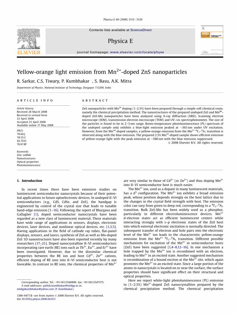
Fig. 1. UV–vis absorption characteristics of the prepared ZnS and ZnS:Mn
nanoparticles.
2. Experimental
Undoped ZnS and Mn+2-doped ZnS:Mn nanoparticles havebeen prepared by a soft chemical approach, namely the chemicalco-precipitation method [3]. All the chemicals used are of ARgrade (Merck and SD fine chemicals), used without furtherpurification. Freshly prepared aqueous solutions of the chemicalsare used for the synthesis of nanoparticles at room temperature.At first, 10 ml each of both zinc nitrate solution and saturatedsolution of sodium sulfide in methanol are prepared. Zinc nitratesolution is first vigorously stirred using a magnetic stirrer up to1 h, and then the solution of sodium sulfide is mixed with thesolution of zinc nitrate dropwise up to pH 8. The precipitate isseparated from the reaction mixture by centrifugation (EltekRefrigerated Centrifuge RC 4100D) for 5 min at 10,000 rpm and iswashed several times with methanol to remove all sodiumparticles. The wet precipitate is then dried up for furthermeasurement and analyses. Mn2+-doped-ZnS nanoparticles wereprepared at room temperature of 20 1C by mixing calculatedamounts of zinc nitrate solution in methanol and manganeseacetate solution in methanol followed by drop wise addition ofsaturated solution of sodium sulfide in methanol up to pH 8. Themixture was vigorously stirred using a magnetic stirrer up to 1 h.The precipitate was separated from the reaction mixture bycentrifugation for 5 min at 10,000 rpm and was washed severaltimes with methanol to remove all sodium particles. The wetprecipitate was then dried up.
The prepared nanoparticles were characterized for their opticaland nanostructural properties. The optical transmission/absorp-tion spectra of ZnS and ZnS:Mn nanocrystallites in methanol wererecorded using a UV–vis spectrophotometer (Hitachi U-3010). Theformation of ZnS and ZnS:Mn nanocrystallites were confirmed byTEM (JEOL 2000 FX 11) micrograph. The XRD pattern was recordedwith an X-ray diffractometer (PANLYTICAL) using Cu Ka radiationof wavelength l ¼ 0.15406 nm in the scan range 2y ¼ 24–751.Scanning electron microscope (SEM with EDXA, Sirion) has beenused for compositional analysis of the prepared ZnS and ZnS:Mnnanocrystallites. The PL spectrum of the ZnS and ZnS:Mnnanoparticles dispersed in methanol has been measured using aspectrofluorimeter (F-2500 FL Spectrophotometer, Hitachi).
3. Results and discussion
Fig. 1 shows the UV–vis absorption characteristics of theprepared ZnS and ZnS:Mn samples. For measuring the absorptioncharacteristics, the nanopowders are first dispersed in methanoland taken in a quartz cuvette. The characteristic absorption peaksdue to the ZnS nanoparticles appear in the wavelength range250–340 nm and this peak position reflects the bandgap of theparticles. The fundamental absorption, which corresponds to
electron excitation from the valance band to conduction band, canbe used to determine the nature and value of the optical bandgapof the prepared ZnS nanoparticles. For obtaining the absorptioncharacteristics of all the samples, at first the transmittance (T) atdifferent wavelengths (l) are measured and then absorptioncoefficients (a) at the corresponding wavelengths l are calculatedusing the Beer–Lambert’s relation (Eq. (1)).
a ¼1
dln
1
T
� �, (1)
where d is the path length. The relation between the incidentphoton energy (hn) and the absorption coefficients (a) is given bythe following relation
ðahnÞ1=m¼ cðhn� EgÞ, (2a)
where c is a constant and Eg is the bandgap of the material and theexponent m depends on the type of the transition. For direct andallowed transition m ¼ 1
2, indirect transition m ¼ 2, and for directforbidden m ¼ 3
2. For calculating the direct bandgap value (ahn)2
versus hn is plotted and it is shown in Fig. 2. By extrapolating thestraight portion of the graph on hn axis at a ¼ 0, the opticalbandgaps are calculated and those are 5.40, 5.36, and 5.16 eV,respectively, for undoped ZnS, ZnS:Mn (1%), and ZnS:Mn (2.5%)nanoparticles. The obtained values of the bandgap of ZnS and Mn-doped ZnS nanoparticles are higher than that of the bulk value ofZnS (3.72 eV). This blue shift of the bandgap takes place because ofthe quantum confinement effect [1]. From the value of thebandgap shift and using Brus model [2] the size of a nanoparticlehas been calculated. For example, the calculated diameter forundoped ZnS is 2.4 nm, which matches well with its average valueof �2.2 nm as obtained from the TEM micrograph.
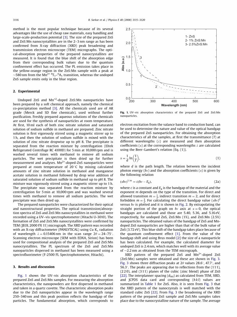
XRD pattern of the prepared ZnS and Mn2+-doped ZnS(ZnS:Mn) samples were obtained and these are shown in Fig. 3.Fig. 3 shows three diffraction peaks at 2y values 28.61, 47.71, and56.31. The peaks are appearing due to reflections from the (111),(2 2 0), and (311) planes of the cubic (zinc blend) phase of ZnS[22]. The interplanner spacing (dhkl) as calculated from TEM, XRD,and JCPDS data card and corresponding (h k l) values aresummarized in Table 1 for ZnS. Also, it is seen from Fig. 3 thatthe XRD pattern of the nanocrystals is well matched with thestandard cubic ZnS [22]. From Fig. 3 the broadening of the XRDpattern of the prepared ZnS sample and ZnS:Mn samples takesplace due to the nanocrystalline nature of the sample. The average
ARTICLE IN PRESS
2.0
ZnS ZnS:Mn (2.5%) ZnS:Mn (1.0%)
Energy (hν, eV)6.05.55.04.54.03.53.02.5
(αhv
)2 (i
n ar
b. u
nit)
Fig. 2. Calculation of optical bandgap from the UV–vis absorption/transmission
spectra.
30
(311)(220)
Inte
nsity
(a.u
)
2θ (deg.)
ZnS
ZnS-1%Mn
ZnS-2.5%Mn
(111)
70605040
Fig. 3. XRD pattern of ZnS and ZnS:Mn. All the graphs are scaled to plot together.
Table 1Interplanner spacing (dhkl) from TEM, XRD, and JCPDS data card and corresponding
(h k l) values for ZnS
dTEM(A) dXRD(A) dJCPDS(A) (h k l)
3.124 3.121 3.123 (111)
1.906 1.906 1.912 (2 2 0)
1.632 1.632 1.633 (311)
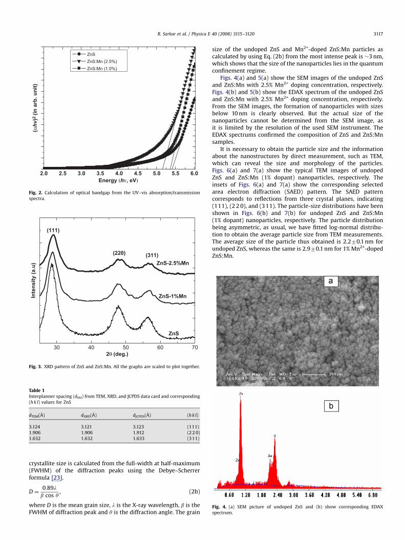
Fig. 4. (a) SEM picture of undoped ZnS and (b) show corresponding EDAX
spectrum.
R. Sarkar et al. / Physica E 40 (2008) 3115–3120 3117
crystallite size is calculated from the full-width at half-maximum(FWHM) of the diffraction peaks using the Debye–Scherrerformula [23].
D ¼0:89lb cos y
, (2b)
where D is the mean grain size, l is the X-ray wavelength, b is theFWHM of diffraction peak and y is the diffraction angle. The grain
size of the undoped ZnS and Mn2+-doped ZnS:Mn particles ascalculated by using Eq. (2b) from the most intense peak is �3 nm,which shows that the size of the nanoparticles lies in the quantumconfinement regime.
Figs. 4(a) and 5(a) show the SEM images of the undoped ZnSand ZnS:Mn with 2.5% Mn2+ doping concentration, respectively.Figs. 4(b) and 5(b) show the EDAX spectrum of the undoped ZnSand ZnS:Mn with 2.5% Mn2+ doping concentration, respectively.From the SEM images, the formation of nanoparticles with sizesbelow 10 nm is clearly observed. But the actual size of thenanoparticles cannot be determined from the SEM image, asit is limited by the resolution of the used SEM instrument. TheEDAX spectrums confirmed the composition of ZnS and ZnS:Mnsamples.
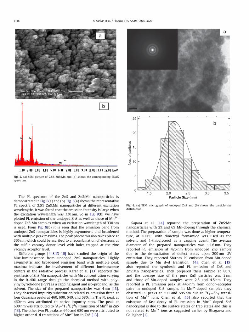
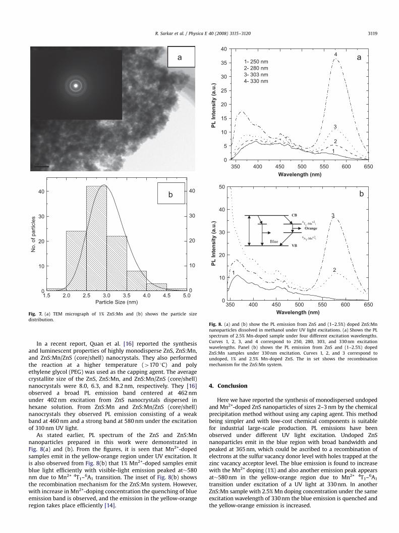
It is necessary to obtain the particle size and the informationabout the nanostructures by direct measurement, such as TEM,which can reveal the size and morphology of the particles.Figs. 6(a) and 7(a) show the typical TEM images of undopedZnS and ZnS:Mn (1% dopant) nanoparticles, respectively. Theinsets of Figs. 6(a) and 7(a) show the corresponding selectedarea electron diffraction (SAED) pattern. The SAED patterncorresponds to reflections from three crystal planes, indicating(111), (2 2 0), and (311). The particle-size distributions have beenshown in Figs. 6(b) and 7(b) for undoped ZnS and ZnS:Mn(1% dopant) nanoparticles, respectively. The particle distributionbeing asymmetric, as usual, we have fitted log-normal distribu-tion to obtain the average particle size from TEM measurements.The average size of the particle thus obtained is 2.270.1 nm forundoped ZnS, whereas the same is 2.970.1 nm for 1% Mn2+-dopedZnS:Mn.
ARTICLE IN PRESS
Fig. 5. (a) SEM picture of 2.5% ZnS:Mn and (b) shows the corresponding EDAX
spectrum.
1.50
5
10
15
20
25
Nos
. of p
artic
les
Particle Size (nm)
b
3.53.02.52.0
a
Fig. 6. (a) TEM micrograph of undoped ZnS and (b) shows the particle-size
distribution.
R. Sarkar et al. / Physica E 40 (2008) 3115–31203118
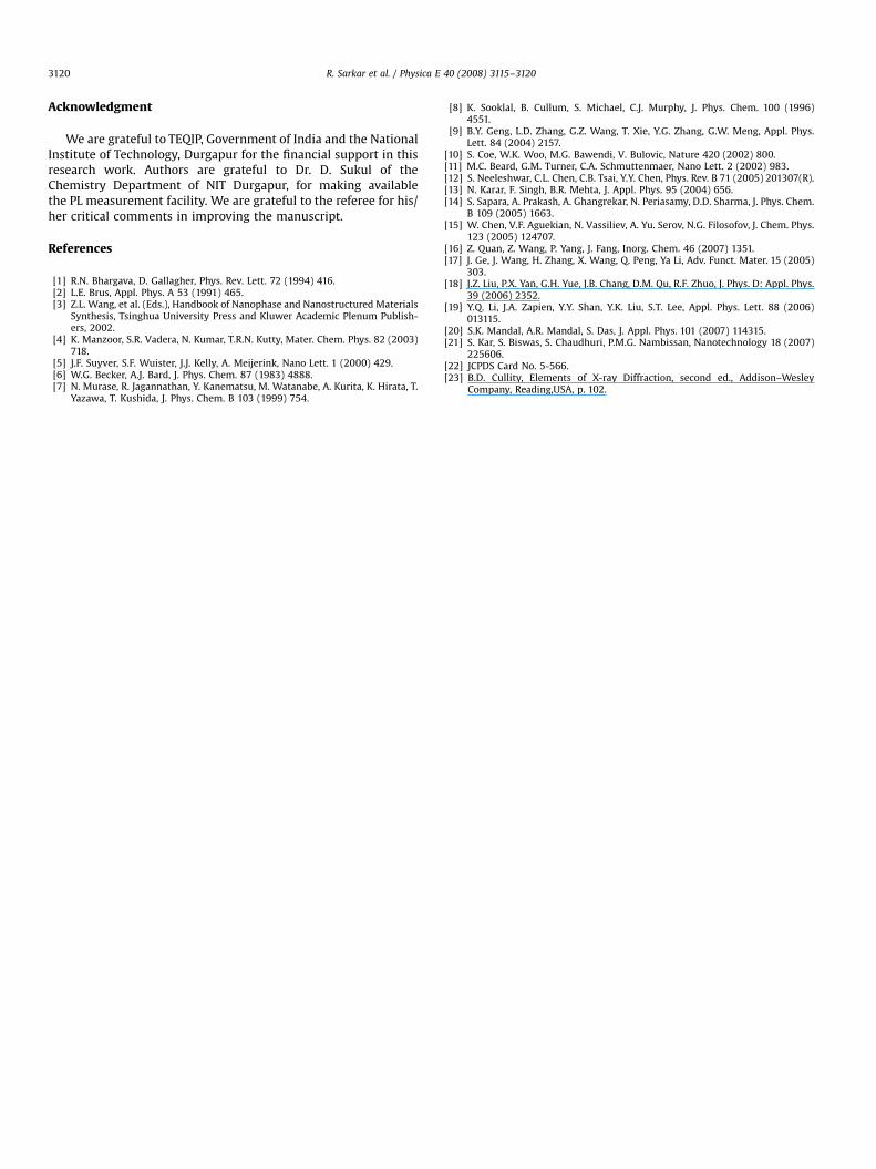
The PL spectrum of the ZnS and ZnS:Mn nanoparticles isdemonstrated in Fig. 8(a) and (b). Fig. 8(a) shows the representativePL spectra of 2.5% ZnS:Mn nanoparticles at different excitationwavelengths. It was found that the emission intensity is large whenthe excitation wavelength was 330 nm. So in Fig. 8(b) we haveplotted PL emission of the undoped ZnS as well as those of Mn2+-doped ZnS:Mn samples when an excitation wavelength of 330 nmis used. From Fig. 8(b) it is seen that the emission band fromundoped ZnS nanoparticles is highly asymmetric and broadenedwith multiple peak maxima. The peak photoemission takes place at365 nm which could be ascribed to a recombination of electrons atthe sulfur vacancy donor level with holes trapped at the zincvacancy acceptor level.
Different groups [4–8,13–16] have studied the origin of theblue-luminescence from undoped ZnS nanoparticles. Highlyasymmetric and broadened emission band with multiple peakmaxima indicate the involvement of different luminescencecenters in the radiative process. Karar et al. [13] reported thesynthesis of ZnS:Mn nanoparticles with Mn concentration varyingin the 0–40% range through the chemical method with poly-vinylpyrrolidone (PVP) as a capping agent and iso-propanol as thesolvent. The size of the prepared nanoparticles was 4 nm [13].They observed impurity substitution related PL emission fitted atfour Gaussian peaks at 460, 600, 640, and 680 nm. The PL peak at460 nm was attributed to native impurity sites. The peak at600 nm was attributed to 6A1–4T1
4E (4G) transition of Mn2+ in ZnS[13]. The other two PL peaks at 640 and 680 nm were attributed tohigher order d–d transitions of Mn2+ ion in ZnS [13].
Sapara et al. [14] reported the preparation of ZnS:Mnnanoparticles with 2% and 6% Mn-doping through the chemicalmethod. The preparation of sample was done at higher tempera-ture, at 100 1C, with dimethyl formamide was used as thesolvent and 1-thioglycerol as a capping agent. The averagediameter of the prepared nanoparticles was �1.6 nm. Theyreported PL emission at 425 nm from undoped ZnS sampledue to the de-excitation of defect states upon 290 nm UVexcitation. They reported 580 nm PL emission from Mn-dopedsample due to Mn d–d transition [14]. Chen et al. [15]also reported the synthesis and PL emission of ZnS andZnS:Mn nanoparticles. They prepared their sample at 80 1Cand the average size of the pure ZnS particles was 3 nmand those of Mn-doped samples were 2.5 and 4.5 nm. Theyreported a PL emission peak at 445 nm from donor–acceptorpairs in undoped ZnS sample. In Mn2+-doped samples theyobserved PL peaks at 590 and 595 nm due to 4T1-
6A1 transi-tion of Mn2+ ions. Chen et al. [15] also reported that theexistence of fast decay of PL emission in Mn2+ doped ZnSnanocrystal is due to the surface states or trap states and this isnot related to Mn2+ ions as suggested earlier by Bhagarva andGallagher [1].
ARTICLE IN PRESS
0
10
20
30
40
1.50
10
20
30
40
No.
of p
artic
les
Particle Size (nm)5.04.54.03.53.02.52.0
b
a
Fig. 7. (a) TEM micrograph of 1% ZnS:Mn and (b) shows the particle size
distribution.
3500
5
10
15
20
25
30
35
40
PL In
tens
ity (a
.u.)
Wavelength (nm)
1- 250 nm 2- 280 nm 3- 303 nm 4- 330 nm
a
b
0
10
20
30
40
50
PL In
tens
ity (a
.u.)
Wavelength (nm)
650600550500450400
350 650600550500450400
Fig. 8. (a) and (b) show the PL emission from ZnS and (1–2.5%) doped ZnS:Mn
nanoparticles dissolved in methanol under UV light excitations. (a) Shows the PL
spectrum of 2.5% Mn-doped sample under four different excitation wavelengths.
Curves 1, 2, 3, and 4 correspond to 250, 280, 303, and 330 nm excitation
wavelengths. Panel (b) shows the PL emission from ZnS and (1–2.5%) doped
ZnS:Mn samples under 330 nm excitation. Curves 1, 2, and 3 correspond to
undoped, 1% and 2.5% Mn-doped ZnS. The in set shows the recombination
mechanism for the ZnS:Mn system.
R. Sarkar et al. / Physica E 40 (2008) 3115–3120 3119
In a recent report, Quan et al. [16] reported the synthesisand luminescent properties of highly monodisperse ZnS, ZnS:Mn,and ZnS:Mn/ZnS (core/shell) nanocrystals. They also performedthe reaction at a higher temperature (4170 1C) and polyethylene glycol (PEG) was used as the capping agent. The averagecrystallite size of the ZnS, ZnS:Mn, and ZnS:Mn/ZnS (core/shell)nanocrystals were 8.0, 6.3, and 8.2 nm, respectively. They [16]observed a broad PL emission band centered at 462 nmunder 402 nm excitation from ZnS nanocrystals dispersed inhexane solution. From ZnS:Mn and ZnS:Mn/ZnS (core/shell)nanocrystals they observed PL emission consisting of a weakband at 460 nm and a strong band at 580 nm under the excitationof 310 nm UV light.
As stated earlier, PL spectrum of the ZnS and ZnS:Mnnanoparticles prepared in this work were demonstrated inFig. 8(a) and (b). From the figures, it is seen that Mn2+-dopedsamples emit in the yellow-orange region under UV excitation. Itis also observed from Fig. 8(b) that 1% Mn2+-doped samples emitblue light efficiently with visible-light emission peaked at�580nm due to Mn2+ 4T1–6A1 transition. The inset of Fig. 8(b) showsthe recombination mechanism for the ZnS:Mn system. However,with increase in Mn2+-doping concentration the quenching of blueemission band is observed, and the emission in the yellow-orangeregion takes place efficiently [14].
4. Conclusion
Here we have reported the synthesis of monodispersed undopedand Mn2+-doped ZnS nanoparticles of sizes 2–3 nm by the chemicalprecipitation method without using any caping agent. This methodbeing simpler and with low-cost chemical components is suitablefor industrial large-scale production. PL emissions have beenobserved under different UV light excitation. Undoped ZnSnanoparticles emit in the blue region with broad bandwidth andpeaked at 365 nm, which could be ascribed to a recombination ofelectrons at the sulfur vacancy donor level with holes trapped at thezinc vacancy acceptor level. The blue emission is found to increasewith the Mn2+ doping (1%) and also another emission peak appearsat�580 nm in the yellow-orange region due to Mn2+ 4T1–6A1
transition under excitation of a UV light at 330 nm. In anotherZnS:Mn sample with 2.5% Mn doping concentration under the sameexcitation wavelength of 330 nm the blue emission is quenched andthe yellow-orange emission is increased.
ARTICLE IN PRESS
R. Sarkar et al. / Physica E 40 (2008) 3115–31203120
Acknowledgment
We are grateful to TEQIP, Government of India and the NationalInstitute of Technology, Durgapur for the financial support in thisresearch work. Authors are grateful to Dr. D. Sukul of theChemistry Department of NIT Durgapur, for making availablethe PL measurement facility. We are grateful to the referee for his/her critical comments in improving the manuscript.
References
[1] R.N. Bhargava, D. Gallagher, Phys. Rev. Lett. 72 (1994) 416.[2] L.E. Brus, Appl. Phys. A 53 (1991) 465.[3] Z.L. Wang, et al. (Eds.), Handbook of Nanophase and Nanostructured Materials
Synthesis, Tsinghua University Press and Kluwer Academic Plenum Publish-ers, 2002.
[4] K. Manzoor, S.R. Vadera, N. Kumar, T.R.N. Kutty, Mater. Chem. Phys. 82 (2003)718.
[5] J.F. Suyver, S.F. Wuister, J.J. Kelly, A. Meijerink, Nano Lett. 1 (2000) 429.[6] W.G. Becker, A.J. Bard, J. Phys. Chem. 87 (1983) 4888.[7] N. Murase, R. Jagannathan, Y. Kanematsu, M. Watanabe, A. Kurita, K. Hirata, T.
Yazawa, T. Kushida, J. Phys. Chem. B 103 (1999) 754.
[8] K. Sooklal, B. Cullum, S. Michael, C.J. Murphy, J. Phys. Chem. 100 (1996)4551.
[9] B.Y. Geng, L.D. Zhang, G.Z. Wang, T. Xie, Y.G. Zhang, G.W. Meng, Appl. Phys.Lett. 84 (2004) 2157.
[10] S. Coe, W.K. Woo, M.G. Bawendi, V. Bulovic, Nature 420 (2002) 800.[11] M.C. Beard, G.M. Turner, C.A. Schmuttenmaer, Nano Lett. 2 (2002) 983.[12] S. Neeleshwar, C.L. Chen, C.B. Tsai, Y.Y. Chen, Phys. Rev. B 71 (2005) 201307(R).[13] N. Karar, F. Singh, B.R. Mehta, J. Appl. Phys. 95 (2004) 656.[14] S. Sapara, A. Prakash, A. Ghangrekar, N. Periasamy, D.D. Sharma, J. Phys. Chem.
B 109 (2005) 1663.[15] W. Chen, V.F. Aguekian, N. Vassiliev, A. Yu. Serov, N.G. Filosofov, J. Chem. Phys.
123 (2005) 124707.[16] Z. Quan, Z. Wang, P. Yang, J. Fang, Inorg. Chem. 46 (2007) 1351.[17] J. Ge, J. Wang, H. Zhang, X. Wang, Q. Peng, Ya Li, Adv. Funct. Mater. 15 (2005)
303.[18] J.Z. Liu, P.X. Yan, G.H. Yue, J.B. Chang, D.M. Qu, R.F. Zhuo, J. Phys. D: Appl. Phys.
39 (2006) 2352.[19] Y.Q. Li, J.A. Zapien, Y.Y. Shan, Y.K. Liu, S.T. Lee, Appl. Phys. Lett. 88 (2006)
013115.[20] S.K. Mandal, A.R. Mandal, S. Das, J. Appl. Phys. 101 (2007) 114315.[21] S. Kar, S. Biswas, S. Chaudhuri, P.M.G. Nambissan, Nanotechnology 18 (2007)
225606.[22] JCPDS Card No. 5-566.[23] B.D. Cullity, Elements of X-ray Diffraction, second ed., Addison–Wesley
Company, Reading,USA, p. 102.