Embed Size (px)
Citation preview
������� ����
�� ����� ������������������� ��� ���������
��� ������
����� ������� ������ �!"#$%&"%������ �������' ������� %�#(#($"&���)��� *������
Copyright 1994 by Siemens Industrial Automation, Inc. All Rights Reserved — Printed in USA
Reproduction, transmission or use of this document orcontents is not permitted without express consent ofSiemens Industrial Automation, Inc. All rights, including rightscreated by patent grant or registration of a utility model ordesign, are reserved.
Since Siemens Industrial Automation, Inc. does not possessfull access to data concerning all of the uses and applicationsof customer’s products, we do not assume responsibility eitherfor customer product design or for any infringements of patentsor rights of others which may result from our assistance.
Technical data is subject to change.
We check the contents of every manual for accuracy at thetime it is approved for printing; however, there may beundetected errors. Any errors found will be corrected insubsequent editions. Any suggestions for improvement arewelcomed.
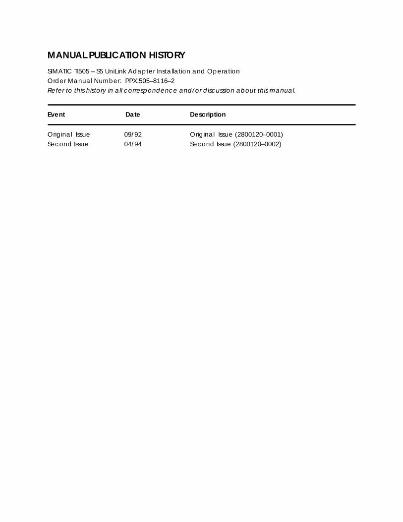
MANUAL PUBLICATION HISTORY
SIMATIC TI505 – S5 UniLink Adapter Installation and OperationOrder Manual Number: PPX:505–8116–2Refer to this history in all correspondence and/or discussion about this manual.
Event Date Description
Original Issue 09/92 Original Issue (2800120–0001)Second Issue 04/94 Second Issue (2800120–0002)
LIST OF EFFECTIVE PAGES
Pages Description Pages Description
Cover/Copyright SecondHistory/Effective Pages Secondiii — x Second
1-1 — 1-5 Second2-1 — 2-8 Second3-1 — 3-12 SecondA-1 — A-11 SecondB-1 — B-9 SecondC-1 — C-3 SecondIndex-1 — Index-3 Second
Registration Second
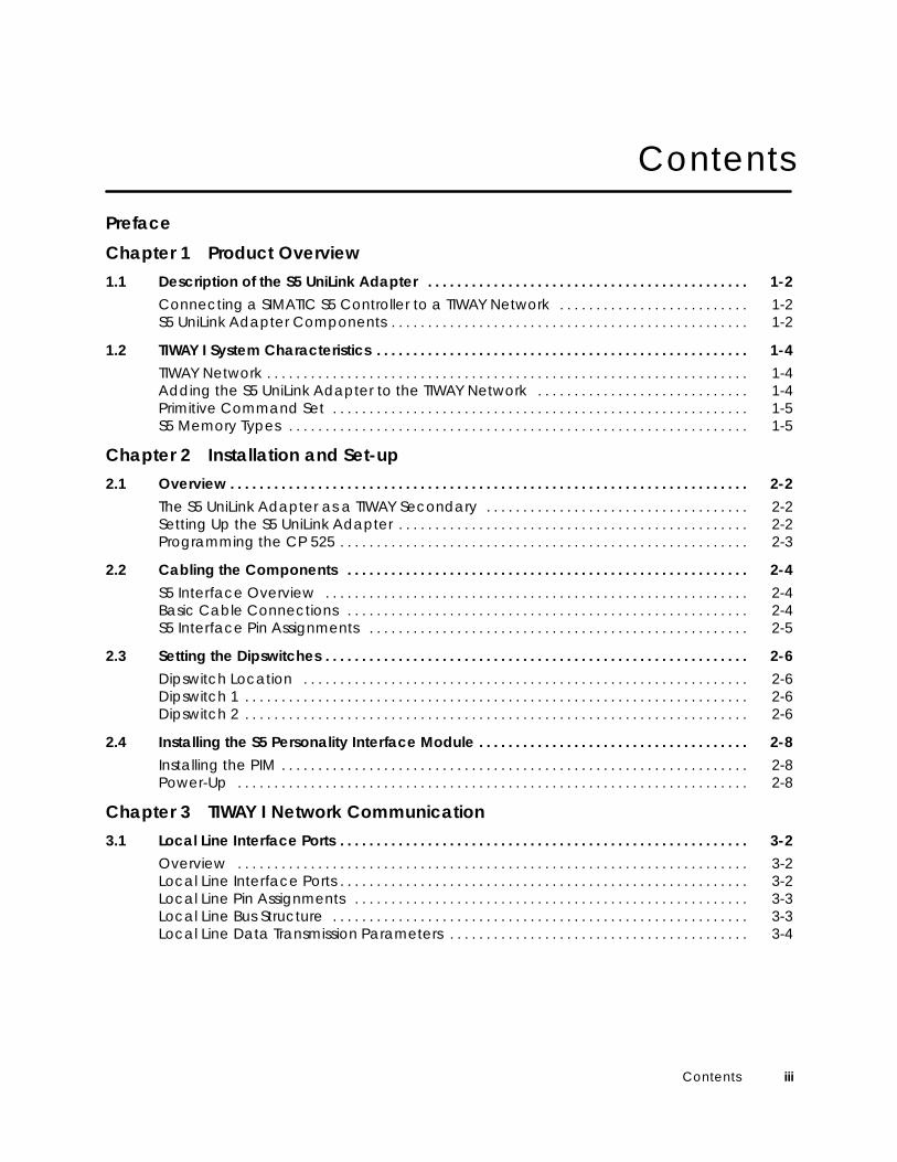
Contents iii
Contents
Preface
Chapter 1 Product Overview1.1 Description of the S5 UniLink Adapter 1-2. . . . . . . . . . . . . . . . . . . . . . . . . . . . . . . . . . . . . . . . . . . .
Connecting a SIMATIC S5 Controller to a TIWAY Network 1-2. . . . . . . . . . . . . . . . . . . . . . . . . . S5 UniLink Adapter Components 1-2. . . . . . . . . . . . . . . . . . . . . . . . . . . . . . . . . . . . . . . . . . . . . . . . .
1.2 TIWAY I System Characteristics 1-4. . . . . . . . . . . . . . . . . . . . . . . . . . . . . . . . . . . . . . . . . . . . . . . . . . . TIWAY Network 1-4. . . . . . . . . . . . . . . . . . . . . . . . . . . . . . . . . . . . . . . . . . . . . . . . . . . . . . . . . . . . . . . . . . Adding the S5 UniLink Adapter to the TIWAY Network 1-4. . . . . . . . . . . . . . . . . . . . . . . . . . . . . Primitive Command Set 1-5. . . . . . . . . . . . . . . . . . . . . . . . . . . . . . . . . . . . . . . . . . . . . . . . . . . . . . . . . S5 Memory Types 1-5. . . . . . . . . . . . . . . . . . . . . . . . . . . . . . . . . . . . . . . . . . . . . . . . . . . . . . . . . . . . . . .
Chapter 2 Installation and Set-up2.1 Overview 2-2. . . . . . . . . . . . . . . . . . . . . . . . . . . . . . . . . . . . . . . . . . . . . . . . . . . . . . . . . . . . . . . . . . . . . . .
The S5 UniLink Adapter as a TIWAY Secondary 2-2. . . . . . . . . . . . . . . . . . . . . . . . . . . . . . . . . . . . Setting Up the S5 UniLink Adapter 2-2. . . . . . . . . . . . . . . . . . . . . . . . . . . . . . . . . . . . . . . . . . . . . . . . Programming the CP 525 2-3. . . . . . . . . . . . . . . . . . . . . . . . . . . . . . . . . . . . . . . . . . . . . . . . . . . . . . . .
2.2 Cabling the Components 2-4. . . . . . . . . . . . . . . . . . . . . . . . . . . . . . . . . . . . . . . . . . . . . . . . . . . . . . . S5 Interface Overview 2-4. . . . . . . . . . . . . . . . . . . . . . . . . . . . . . . . . . . . . . . . . . . . . . . . . . . . . . . . . . Basic Cable Connections 2-4. . . . . . . . . . . . . . . . . . . . . . . . . . . . . . . . . . . . . . . . . . . . . . . . . . . . . . . S5 Interface Pin Assignments 2-5. . . . . . . . . . . . . . . . . . . . . . . . . . . . . . . . . . . . . . . . . . . . . . . . . . . .
2.3 Setting the Dipswitches 2-6. . . . . . . . . . . . . . . . . . . . . . . . . . . . . . . . . . . . . . . . . . . . . . . . . . . . . . . . . . Dipswitch Location 2-6. . . . . . . . . . . . . . . . . . . . . . . . . . . . . . . . . . . . . . . . . . . . . . . . . . . . . . . . . . . . . Dipswitch 1 2-6. . . . . . . . . . . . . . . . . . . . . . . . . . . . . . . . . . . . . . . . . . . . . . . . . . . . . . . . . . . . . . . . . . . . . Dipswitch 2 2-6. . . . . . . . . . . . . . . . . . . . . . . . . . . . . . . . . . . . . . . . . . . . . . . . . . . . . . . . . . . . . . . . . . . . .
2.4 Installing the S5 Personality Interface Module 2-8. . . . . . . . . . . . . . . . . . . . . . . . . . . . . . . . . . . . . Installing the PIM 2-8. . . . . . . . . . . . . . . . . . . . . . . . . . . . . . . . . . . . . . . . . . . . . . . . . . . . . . . . . . . . . . . . Power-Up 2-8. . . . . . . . . . . . . . . . . . . . . . . . . . . . . . . . . . . . . . . . . . . . . . . . . . . . . . . . . . . . . . . . . . . . . .
Chapter 3 TIWAY I Network Communication3.1 Local Line Interface Ports 3-2. . . . . . . . . . . . . . . . . . . . . . . . . . . . . . . . . . . . . . . . . . . . . . . . . . . . . . . .
Overview 3-2. . . . . . . . . . . . . . . . . . . . . . . . . . . . . . . . . . . . . . . . . . . . . . . . . . . . . . . . . . . . . . . . . . . . . . Local Line Interface Ports 3-2. . . . . . . . . . . . . . . . . . . . . . . . . . . . . . . . . . . . . . . . . . . . . . . . . . . . . . . . Local Line Pin Assignments 3-3. . . . . . . . . . . . . . . . . . . . . . . . . . . . . . . . . . . . . . . . . . . . . . . . . . . . . . Local Line Bus Structure 3-3. . . . . . . . . . . . . . . . . . . . . . . . . . . . . . . . . . . . . . . . . . . . . . . . . . . . . . . . . Local Line Data Transmission Parameters 3-4. . . . . . . . . . . . . . . . . . . . . . . . . . . . . . . . . . . . . . . . .
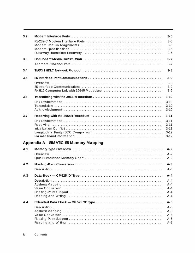
iv Contents
3.2 Modem Interface Ports 3-5. . . . . . . . . . . . . . . . . . . . . . . . . . . . . . . . . . . . . . . . . . . . . . . . . . . . . . . . . . RS-232-C Modem Interface Ports 3-5. . . . . . . . . . . . . . . . . . . . . . . . . . . . . . . . . . . . . . . . . . . . . . . . Modem Port Pin Assignments 3-5. . . . . . . . . . . . . . . . . . . . . . . . . . . . . . . . . . . . . . . . . . . . . . . . . . . . Modem Specifications 3-6. . . . . . . . . . . . . . . . . . . . . . . . . . . . . . . . . . . . . . . . . . . . . . . . . . . . . . . . . . Runaway Transmitter Recovery 3-6. . . . . . . . . . . . . . . . . . . . . . . . . . . . . . . . . . . . . . . . . . . . . . . . . .
3.3 Redundant Media Transmission 3-7. . . . . . . . . . . . . . . . . . . . . . . . . . . . . . . . . . . . . . . . . . . . . . . . . . Alternate Channel Port 3-7. . . . . . . . . . . . . . . . . . . . . . . . . . . . . . . . . . . . . . . . . . . . . . . . . . . . . . . . .
3.4 TIWAY I HDLC Network Protocol 3-8. . . . . . . . . . . . . . . . . . . . . . . . . . . . . . . . . . . . . . . . . . . . . . . . . .
3.5 S5 Interface Port Communications 3-9. . . . . . . . . . . . . . . . . . . . . . . . . . . . . . . . . . . . . . . . . . . . . . . Overview 3-9. . . . . . . . . . . . . . . . . . . . . . . . . . . . . . . . . . . . . . . . . . . . . . . . . . . . . . . . . . . . . . . . . . . . . . S5 Interface Communications 3-9. . . . . . . . . . . . . . . . . . . . . . . . . . . . . . . . . . . . . . . . . . . . . . . . . . . RK 512 Computer Link with 3964R Procedure 3-9. . . . . . . . . . . . . . . . . . . . . . . . . . . . . . . . . . . . .
3.6 Transmitting with the 3964R Procedure 3-10. . . . . . . . . . . . . . . . . . . . . . . . . . . . . . . . . . . . . . . . . . . . Link Establishment 3-10. . . . . . . . . . . . . . . . . . . . . . . . . . . . . . . . . . . . . . . . . . . . . . . . . . . . . . . . . . . . . . . Transmission 3-10. . . . . . . . . . . . . . . . . . . . . . . . . . . . . . . . . . . . . . . . . . . . . . . . . . . . . . . . . . . . . . . . . . . . Acknowledgment 3-10. . . . . . . . . . . . . . . . . . . . . . . . . . . . . . . . . . . . . . . . . . . . . . . . . . . . . . . . . . . . . .
3.7 Receiving with the 3964R Procedure 3-11. . . . . . . . . . . . . . . . . . . . . . . . . . . . . . . . . . . . . . . . . . . . . Link Establishment 3-11. . . . . . . . . . . . . . . . . . . . . . . . . . . . . . . . . . . . . . . . . . . . . . . . . . . . . . . . . . . . . . . Receiving 3-11. . . . . . . . . . . . . . . . . . . . . . . . . . . . . . . . . . . . . . . . . . . . . . . . . . . . . . . . . . . . . . . . . . . . . . Initialization Conflict 3-11. . . . . . . . . . . . . . . . . . . . . . . . . . . . . . . . . . . . . . . . . . . . . . . . . . . . . . . . . . . . . Longitudinal Parity (BCC Comparison) 3-12. . . . . . . . . . . . . . . . . . . . . . . . . . . . . . . . . . . . . . . . . . . For Additional Information 3-12. . . . . . . . . . . . . . . . . . . . . . . . . . . . . . . . . . . . . . . . . . . . . . . . . . . . . . .
Appendix A SIMATIC S5 Memory Mapping
A.1 Memory Type Overview A-2. . . . . . . . . . . . . . . . . . . . . . . . . . . . . . . . . . . . . . . . . . . . . . . . . . . . . . . . . Overview A-2. . . . . . . . . . . . . . . . . . . . . . . . . . . . . . . . . . . . . . . . . . . . . . . . . . . . . . . . . . . . . . . . . . . . . . Quick Reference Memory Chart A-2. . . . . . . . . . . . . . . . . . . . . . . . . . . . . . . . . . . . . . . . . . . . . . . . .
A.2 Floating-Point Conversion A-3. . . . . . . . . . . . . . . . . . . . . . . . . . . . . . . . . . . . . . . . . . . . . . . . . . . . . . . Description A-3. . . . . . . . . . . . . . . . . . . . . . . . . . . . . . . . . . . . . . . . . . . . . . . . . . . . . . . . . . . . . . . . . . . . .
A.3 Data Block — CP 525 ‘D’ Type A-4. . . . . . . . . . . . . . . . . . . . . . . . . . . . . . . . . . . . . . . . . . . . . . . . . . . Description A-4. . . . . . . . . . . . . . . . . . . . . . . . . . . . . . . . . . . . . . . . . . . . . . . . . . . . . . . . . . . . . . . . . . . . . Address Mapping A-4. . . . . . . . . . . . . . . . . . . . . . . . . . . . . . . . . . . . . . . . . . . . . . . . . . . . . . . . . . . . . . . Value Conversion A-4. . . . . . . . . . . . . . . . . . . . . . . . . . . . . . . . . . . . . . . . . . . . . . . . . . . . . . . . . . . . . . . Floating-Point Support A-4. . . . . . . . . . . . . . . . . . . . . . . . . . . . . . . . . . . . . . . . . . . . . . . . . . . . . . . . . . . Reading and Writing A-4. . . . . . . . . . . . . . . . . . . . . . . . . . . . . . . . . . . . . . . . . . . . . . . . . . . . . . . . . . . .
A.4 Extended Data Block — CP 525 ‘X’ Type A-5. . . . . . . . . . . . . . . . . . . . . . . . . . . . . . . . . . . . . . . . . . Description A-5. . . . . . . . . . . . . . . . . . . . . . . . . . . . . . . . . . . . . . . . . . . . . . . . . . . . . . . . . . . . . . . . . . . . . Address Mapping A-5. . . . . . . . . . . . . . . . . . . . . . . . . . . . . . . . . . . . . . . . . . . . . . . . . . . . . . . . . . . . . . . Value Conversion A-5. . . . . . . . . . . . . . . . . . . . . . . . . . . . . . . . . . . . . . . . . . . . . . . . . . . . . . . . . . . . . . . Floating-Point Support A-5. . . . . . . . . . . . . . . . . . . . . . . . . . . . . . . . . . . . . . . . . . . . . . . . . . . . . . . . . . . Reading and Writing A-5. . . . . . . . . . . . . . . . . . . . . . . . . . . . . . . . . . . . . . . . . . . . . . . . . . . . . . . . . . . .
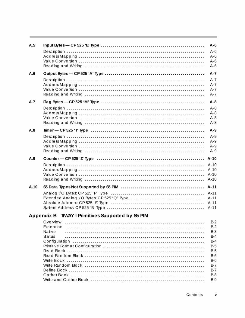
Contents v
A.5 Input Bytes — CP 525 ‘E’ Type A-6. . . . . . . . . . . . . . . . . . . . . . . . . . . . . . . . . . . . . . . . . . . . . . . . . . . . Description A-6. . . . . . . . . . . . . . . . . . . . . . . . . . . . . . . . . . . . . . . . . . . . . . . . . . . . . . . . . . . . . . . . . . . . . Address Mapping A-6. . . . . . . . . . . . . . . . . . . . . . . . . . . . . . . . . . . . . . . . . . . . . . . . . . . . . . . . . . . . . . . Value Conversion A-6. . . . . . . . . . . . . . . . . . . . . . . . . . . . . . . . . . . . . . . . . . . . . . . . . . . . . . . . . . . . . . . Reading and Writing A-6. . . . . . . . . . . . . . . . . . . . . . . . . . . . . . . . . . . . . . . . . . . . . . . . . . . . . . . . . . . .
A.6 Output Bytes — CP 525 ‘A’ Type A-7. . . . . . . . . . . . . . . . . . . . . . . . . . . . . . . . . . . . . . . . . . . . . . . . . . Description A-7. . . . . . . . . . . . . . . . . . . . . . . . . . . . . . . . . . . . . . . . . . . . . . . . . . . . . . . . . . . . . . . . . . . . . Address Mapping A-7. . . . . . . . . . . . . . . . . . . . . . . . . . . . . . . . . . . . . . . . . . . . . . . . . . . . . . . . . . . . . . . Value Conversion A-7. . . . . . . . . . . . . . . . . . . . . . . . . . . . . . . . . . . . . . . . . . . . . . . . . . . . . . . . . . . . . . . Reading and Writing A-7. . . . . . . . . . . . . . . . . . . . . . . . . . . . . . . . . . . . . . . . . . . . . . . . . . . . . . . . . . . .
A.7 Flag Bytes — CP 525 ‘M’ Type A-8. . . . . . . . . . . . . . . . . . . . . . . . . . . . . . . . . . . . . . . . . . . . . . . . . . . . Description A-8. . . . . . . . . . . . . . . . . . . . . . . . . . . . . . . . . . . . . . . . . . . . . . . . . . . . . . . . . . . . . . . . . . . . . Address Mapping A-8. . . . . . . . . . . . . . . . . . . . . . . . . . . . . . . . . . . . . . . . . . . . . . . . . . . . . . . . . . . . . . . Value Conversion A-8. . . . . . . . . . . . . . . . . . . . . . . . . . . . . . . . . . . . . . . . . . . . . . . . . . . . . . . . . . . . . . . Reading and Writing A-8. . . . . . . . . . . . . . . . . . . . . . . . . . . . . . . . . . . . . . . . . . . . . . . . . . . . . . . . . . . .
A.8 Timer — CP 525 ‘T’ Type A-9. . . . . . . . . . . . . . . . . . . . . . . . . . . . . . . . . . . . . . . . . . . . . . . . . . . . . . . . . Description A-9. . . . . . . . . . . . . . . . . . . . . . . . . . . . . . . . . . . . . . . . . . . . . . . . . . . . . . . . . . . . . . . . . . . . . Address Mapping A-9. . . . . . . . . . . . . . . . . . . . . . . . . . . . . . . . . . . . . . . . . . . . . . . . . . . . . . . . . . . . . . . Value Conversion A-9. . . . . . . . . . . . . . . . . . . . . . . . . . . . . . . . . . . . . . . . . . . . . . . . . . . . . . . . . . . . . . . Reading and Writing A-9. . . . . . . . . . . . . . . . . . . . . . . . . . . . . . . . . . . . . . . . . . . . . . . . . . . . . . . . . . . .
A.9 Counter — CP 525 ‘Z’ Type A-10. . . . . . . . . . . . . . . . . . . . . . . . . . . . . . . . . . . . . . . . . . . . . . . . . . . . . . Description A-10. . . . . . . . . . . . . . . . . . . . . . . . . . . . . . . . . . . . . . . . . . . . . . . . . . . . . . . . . . . . . . . . . . . . . Address Mapping A-10. . . . . . . . . . . . . . . . . . . . . . . . . . . . . . . . . . . . . . . . . . . . . . . . . . . . . . . . . . . . . . . Value Conversion A-10. . . . . . . . . . . . . . . . . . . . . . . . . . . . . . . . . . . . . . . . . . . . . . . . . . . . . . . . . . . . . . . Reading and Writing A-10. . . . . . . . . . . . . . . . . . . . . . . . . . . . . . . . . . . . . . . . . . . . . . . . . . . . . . . . . . . .
A.10 S5 Data Types Not Supported by S5 PIM A-11. . . . . . . . . . . . . . . . . . . . . . . . . . . . . . . . . . . . . . . . . . Analog I/O Bytes: CP 525 ‘P’ Type A-11. . . . . . . . . . . . . . . . . . . . . . . . . . . . . . . . . . . . . . . . . . . . . . . Extended Analog I/O Bytes: CP 525 ‘Q’ Type A-11. . . . . . . . . . . . . . . . . . . . . . . . . . . . . . . . . . . . . Absolute Address: CP 525 ‘S’ Type A-11. . . . . . . . . . . . . . . . . . . . . . . . . . . . . . . . . . . . . . . . . . . . . . . System Address: CP 525 ‘B’ Type A-11. . . . . . . . . . . . . . . . . . . . . . . . . . . . . . . . . . . . . . . . . . . . . . . . .
Appendix B TIWAY I Primitives Supported by S5 PIMOverview B-2. . . . . . . . . . . . . . . . . . . . . . . . . . . . . . . . . . . . . . . . . . . . . . . . . . . . . . . . . . . . . . . . . . . . . . Exception B-2. . . . . . . . . . . . . . . . . . . . . . . . . . . . . . . . . . . . . . . . . . . . . . . . . . . . . . . . . . . . . . . . . . . . . . Native B-3. . . . . . . . . . . . . . . . . . . . . . . . . . . . . . . . . . . . . . . . . . . . . . . . . . . . . . . . . . . . . . . . . . . . . . Status B-4. . . . . . . . . . . . . . . . . . . . . . . . . . . . . . . . . . . . . . . . . . . . . . . . . . . . . . . . . . . . . . . . . . . . . . Configuration B-4. . . . . . . . . . . . . . . . . . . . . . . . . . . . . . . . . . . . . . . . . . . . . . . . . . . . . . . . . . . . . . . . . . Primitive Format Configuration B-5. . . . . . . . . . . . . . . . . . . . . . . . . . . . . . . . . . . . . . . . . . . . . . . . . . . Read Block B-5. . . . . . . . . . . . . . . . . . . . . . . . . . . . . . . . . . . . . . . . . . . . . . . . . . . . . . . . . . . . . . . . . . . . . Read Random Block B-6. . . . . . . . . . . . . . . . . . . . . . . . . . . . . . . . . . . . . . . . . . . . . . . . . . . . . . . . . . . . Write Block B-6. . . . . . . . . . . . . . . . . . . . . . . . . . . . . . . . . . . . . . . . . . . . . . . . . . . . . . . . . . . . . . . . . . . . . Write Random Block B-7. . . . . . . . . . . . . . . . . . . . . . . . . . . . . . . . . . . . . . . . . . . . . . . . . . . . . . . . . . . . Define Block B-7. . . . . . . . . . . . . . . . . . . . . . . . . . . . . . . . . . . . . . . . . . . . . . . . . . . . . . . . . . . . . . . . . . . . Gather Block B-8. . . . . . . . . . . . . . . . . . . . . . . . . . . . . . . . . . . . . . . . . . . . . . . . . . . . . . . . . . . . . . . . . . . Write and Gather Block B-9. . . . . . . . . . . . . . . . . . . . . . . . . . . . . . . . . . . . . . . . . . . . . . . . . . . . . . . . .
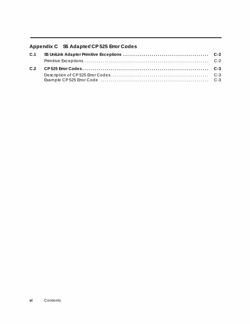
vi Contents
Appendix C S5 Adapter/CP 525 Error CodesC.1 S5 UniLink Adapter Primitive Exceptions C-2. . . . . . . . . . . . . . . . . . . . . . . . . . . . . . . . . . . . . . . . . .
Primitive Exceptions C-2. . . . . . . . . . . . . . . . . . . . . . . . . . . . . . . . . . . . . . . . . . . . . . . . . . . . . . . . . . . . .
C.2 CP 525 Error Codes C-3. . . . . . . . . . . . . . . . . . . . . . . . . . . . . . . . . . . . . . . . . . . . . . . . . . . . . . . . . . . . . . Description of CP 525 Error Codes C-3. . . . . . . . . . . . . . . . . . . . . . . . . . . . . . . . . . . . . . . . . . . . . . . . Example CP 525 Error Code C-3. . . . . . . . . . . . . . . . . . . . . . . . . . . . . . . . . . . . . . . . . . . . . . . . . . . . .
Contents vii
List of Figures
1-1 S5 UniLink Adapter Interface 1-2. . . . . . . . . . . . . . . . . . . . . . . . . . . . . . . . . . . . . . . . . . . . . . . . . . . . 1-2 S5 UniLink Adapter 1-3. . . . . . . . . . . . . . . . . . . . . . . . . . . . . . . . . . . . . . . . . . . . . . . . . . . . . . . . . . . . . . 1-3 S5 Personality Interface Module (PIM) 1-3. . . . . . . . . . . . . . . . . . . . . . . . . . . . . . . . . . . . . . . . . . . . 1-4 S5 UniLink Adapter in a TIWAY I Network 1-4. . . . . . . . . . . . . . . . . . . . . . . . . . . . . . . . . . . . . . . . . . 1-5 S5 UniLink Adapter Primitives 1-5. . . . . . . . . . . . . . . . . . . . . . . . . . . . . . . . . . . . . . . . . . . . . . . . . . . . . 1-6 S5 UniLink Adapter Memory Types 1-5. . . . . . . . . . . . . . . . . . . . . . . . . . . . . . . . . . . . . . . . . . . . . . .
2-1 Main Steps for Setting up the S5 UniLink Adapter 2-2. . . . . . . . . . . . . . . . . . . . . . . . . . . . . . . . . . 2-2 S5 UniLink Adapter Interface 2-4. . . . . . . . . . . . . . . . . . . . . . . . . . . . . . . . . . . . . . . . . . . . . . . . . . . . 2-3 Pin Assignments for Connecting S5 Adapter to CP 525 2-5. . . . . . . . . . . . . . . . . . . . . . . . . . . . 2-4 S5 UniLink Adapter Dipswitch Location 2-6. . . . . . . . . . . . . . . . . . . . . . . . . . . . . . . . . . . . . . . . . . . 2-5 S5 UniLink Dipswitch 1 Settings 2-7. . . . . . . . . . . . . . . . . . . . . . . . . . . . . . . . . . . . . . . . . . . . . . . . . . . 2-6 S5 UniLink Dipswitch 2 Settings 2-7. . . . . . . . . . . . . . . . . . . . . . . . . . . . . . . . . . . . . . . . . . . . . . . . . . . 2-7 Installing the S5 PIM 2-8. . . . . . . . . . . . . . . . . . . . . . . . . . . . . . . . . . . . . . . . . . . . . . . . . . . . . . . . . . . . .
3-1 Local Line Interface Ports 3-2. . . . . . . . . . . . . . . . . . . . . . . . . . . . . . . . . . . . . . . . . . . . . . . . . . . . . . . . 3-2 TIWAY I Bus Structure 3-3. . . . . . . . . . . . . . . . . . . . . . . . . . . . . . . . . . . . . . . . . . . . . . . . . . . . . . . . . . . . 3-3 Number of Local Line Secondaries vs. Cable Distance 3-4. . . . . . . . . . . . . . . . . . . . . . . . . . . . 3-4 RS-232/RS-423 Modem Interface Ports 3-5. . . . . . . . . . . . . . . . . . . . . . . . . . . . . . . . . . . . . . . . . . . . 3-5 Redundant Media Circuit 3-7. . . . . . . . . . . . . . . . . . . . . . . . . . . . . . . . . . . . . . . . . . . . . . . . . . . . . . . 3-6 HDLC Information Frame 3-8. . . . . . . . . . . . . . . . . . . . . . . . . . . . . . . . . . . . . . . . . . . . . . . . . . . . . . . .
A-1 IEEE Floating-Point Value A-3. . . . . . . . . . . . . . . . . . . . . . . . . . . . . . . . . . . . . . . . . . . . . . . . . . . . . . . . A-2 S5 Floating-Point Value A-3. . . . . . . . . . . . . . . . . . . . . . . . . . . . . . . . . . . . . . . . . . . . . . . . . . . . . . . . . .
viii Contents
List of Tables
1 S5 UniLink Adapter Models x. . . . . . . . . . . . . . . . . . . . . . . . . . . . . . . . . . . . . . . . . . . . . . . . . . . . . .
3-1 S5 UniLink Adapter Models 3-2. . . . . . . . . . . . . . . . . . . . . . . . . . . . . . . . . . . . . . . . . . . . . . . . . . . . . . 3-2 Local Line Connector Pin Assignments 3-3. . . . . . . . . . . . . . . . . . . . . . . . . . . . . . . . . . . . . . . . . . . 3-3 RS-232/RS-423 D Connector Pin Assignments 3-5. . . . . . . . . . . . . . . . . . . . . . . . . . . . . . . . . . . . . .
A-1 TI500/TI505 vs. S5 Memory Types A-2. . . . . . . . . . . . . . . . . . . . . . . . . . . . . . . . . . . . . . . . . . . . . . . . .
C-1 Primitive Exception Error Byte C-2. . . . . . . . . . . . . . . . . . . . . . . . . . . . . . . . . . . . . . . . . . . . . . . . . . . . C-2 CP 525 Error Code C-3. . . . . . . . . . . . . . . . . . . . . . . . . . . . . . . . . . . . . . . . . . . . . . . . . . . . . . . . . . . . . .
Preface ixS5 UniLink Adapter Installation and Operation
Preface
This manual is intended to help you accomplish the tasks required to installand operate the S5 UniLink Adapter with the SIMATIC S5 PersonalityInterface Module (PIM).
This manual assumes that you are already familiar with the contents of theTIWAY I Systems Manual and the UNILINK Adapter Installation &Operation Manual.
The information in this manual is supplemented by the following manuals.
• TIWAY I Systems Manual (PPX:TIWAY–8101)
• TIWAY I UNILINK Host Adapter User’s Manual (PPX:TIWAY–8121)
• UNILINK Adapter Installation and Operation Manual(PPX:TIWAY–8106)
The TIWAY I System Manual provides more information on the installationand operation of your TIWAY I network. The UNILINK Adapter Installation& Operation Manual details the installation and operation of the UNILINKAdapter. Refer also to the user manuals for any other TIWAY I networkdevices that you have installed or will be installing.
Additional information is found in the following SIMATIC S5 manuals.
• COM 525 Manual, Volumes 1 and 2 (6ES5 998–1DB21)
• Automating with the SIMATIC S5–135U (A19100-L531-F505-X-7600)
The COM 525 Manuals provide complete information on installing andprogramming your CP 525 module. The Automating with the SIMATICS5–135U manual provides a thorough background of the SIMATIC S5 135Uprogrammable controller (PLC).
NOTE: Throughout this manual, all references to the CP 525 module applyequally to the CP 524 module, as both of these models are compatible withthe S5 UniLink Adapter.
Purpose of thisManual
Related Manuals
Prefacex S5 UniLink Adapter Installation and Operation
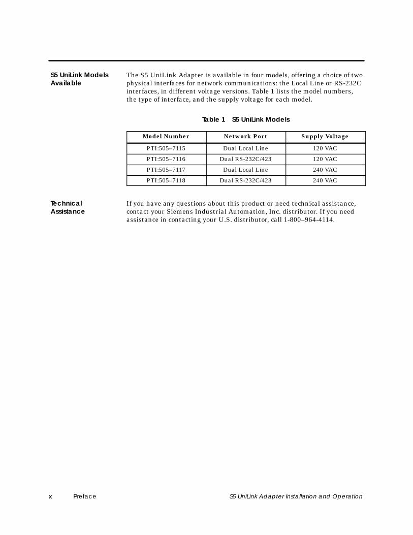
The S5 UniLink Adapter is available in four models, offering a choice of twophysical interfaces for network communications: the Local Line or RS-232Cinterfaces, in different voltage versions. Table 1 lists the model numbers,the type of interface, and the supply voltage for each model.
Table 1 S5 UniLink Models
Model Number Network Port Supply Voltage
PTI:505–7115 Dual Local Line 120 VAC
PTI:505–7116 Dual RS-232C/423 120 VAC
PTI:505–7117 Dual Local Line 240 VAC
PTI:505–7118 Dual RS-232C/423 240 VAC
If you have any questions about this product or need technical assistance,contact your Siemens Industrial Automation, Inc. distributor. If you needassistance in contacting your U.S. distributor, call 1-800–964-4114.
S5 UniLink ModelsAvailable
TechnicalAssistance
Product Overview 1-1S5 UniLink Adapter Installation and Operation
Chapter 1
Product Overview
1.1 Description of the S5 UniLink Adapter 1-2. . . . . . . . . . . . . . . . . . . . . . . . . . . . . . . . . . . . . . . . . . . . Connecting a SIMATIC S5 Controller to a TIWAY Network 1-2. . . . . . . . . . . . . . . . . . . . . . . . . . S5 UniLink Adapter Components 1-2. . . . . . . . . . . . . . . . . . . . . . . . . . . . . . . . . . . . . . . . . . . . . . . . .
1.2 TIWAY I System Characteristics 1-4. . . . . . . . . . . . . . . . . . . . . . . . . . . . . . . . . . . . . . . . . . . . . . . . . . . TIWAY Network 1-4. . . . . . . . . . . . . . . . . . . . . . . . . . . . . . . . . . . . . . . . . . . . . . . . . . . . . . . . . . . . . . . . . . Adding the S5 UniLink Adapter to the TIWAY Network 1-4. . . . . . . . . . . . . . . . . . . . . . . . . . . . . Primitive Command Set 1-5. . . . . . . . . . . . . . . . . . . . . . . . . . . . . . . . . . . . . . . . . . . . . . . . . . . . . . . . . S5 Memory Types 1-5. . . . . . . . . . . . . . . . . . . . . . . . . . . . . . . . . . . . . . . . . . . . . . . . . . . . . . . . . . . . . . .
Product Overview1-2 S5 UniLink Adapter Installation and Operation
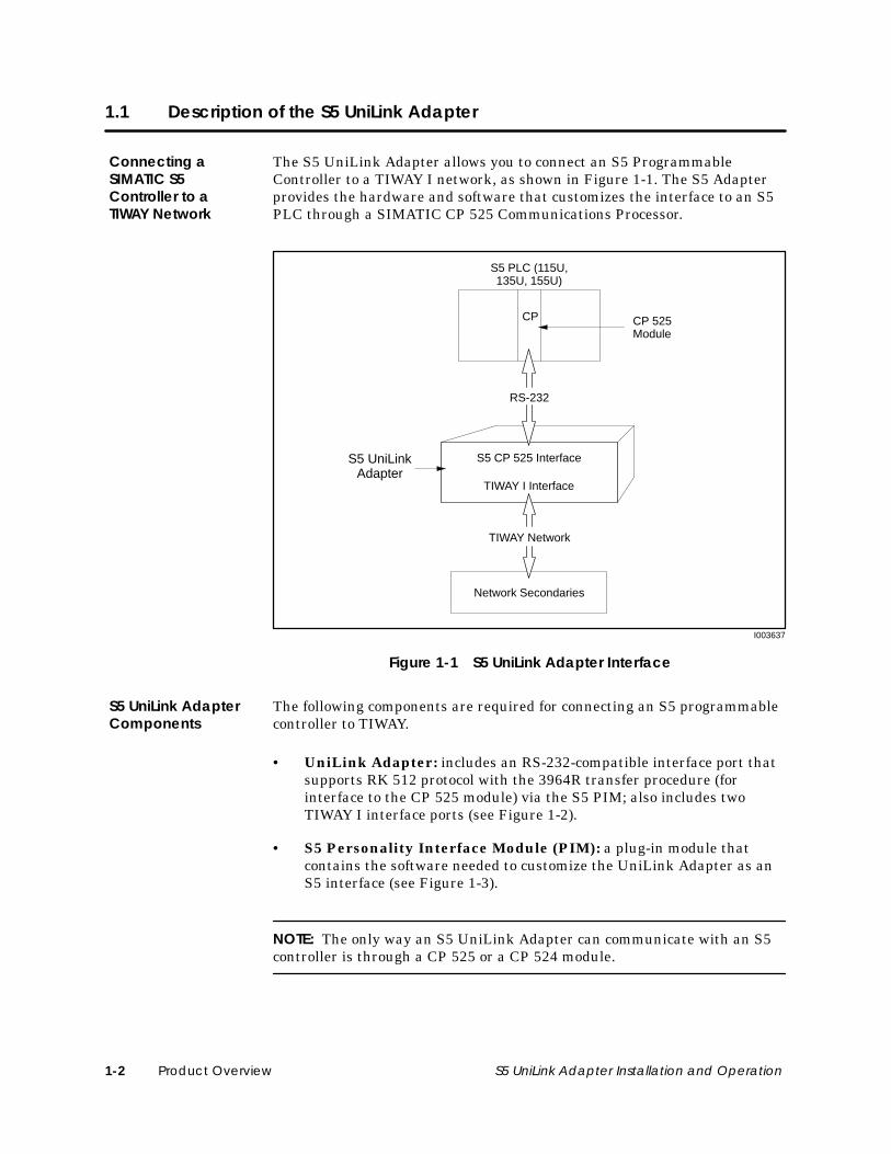
1.1 Description of the S5 UniLink Adapter
The S5 UniLink Adapter allows you to connect an S5 ProgrammableController to a TIWAY I network, as shown in Figure 1-1. The S5 Adapterprovides the hardware and software that customizes the interface to an S5PLC through a SIMATIC CP 525 Communications Processor.
I003637
S5 PLC (115U,135U, 155U)
CP 525Module
RS-232
S5 CP 525 Interface
TIWAY I Interface
TIWAY Network
Network Secondaries
S5 UniLinkAdapter
CP
Figure 1-1 S5 UniLink Adapter Interface
The following components are required for connecting an S5 programmablecontroller to TIWAY.
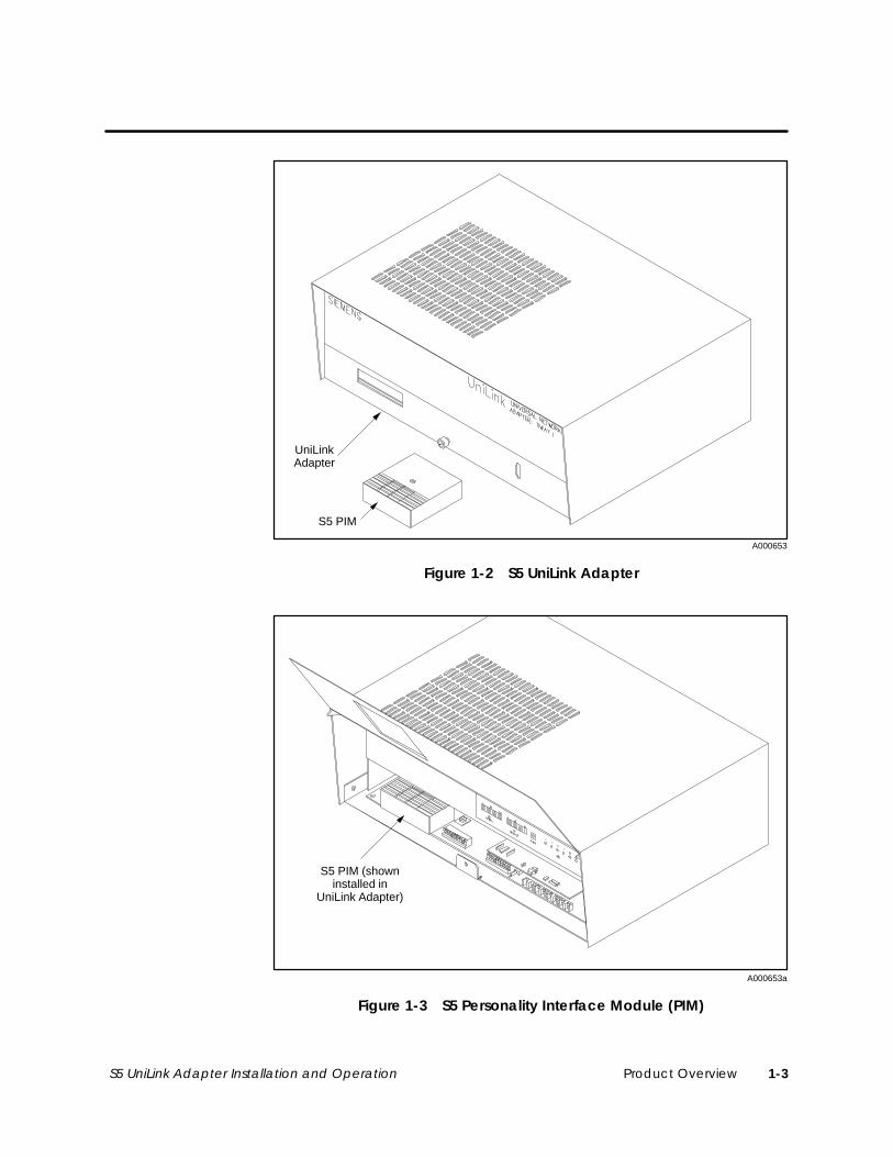
• UniLink Adapter: includes an RS-232-compatible interface port thatsupports RK 512 protocol with the 3964R transfer procedure (forinterface to the CP 525 module) via the S5 PIM; also includes twoTIWAY I interface ports (see Figure 1-2).
• S5 Personality Interface Module (PIM): a plug-in module thatcontains the software needed to customize the UniLink Adapter as anS5 interface (see Figure 1-3).
NOTE: The only way an S5 UniLink Adapter can communicate with an S5controller is through a CP 525 or a CP 524 module.
Connecting aSIMATIC S5Controller to aTIWAY Network
S5 UniLink AdapterComponents
Product Overview 1-3S5 UniLink Adapter Installation and Operation
A000653
UniLinkAdapter
S5 PIM
Figure 1-2 S5 UniLink Adapter
A000653a
S5 PIM (showninstalled in
UniLink Adapter)
Figure 1-3 S5 Personality Interface Module (PIM)
Product Overview1-4 S5 UniLink Adapter Installation and Operation
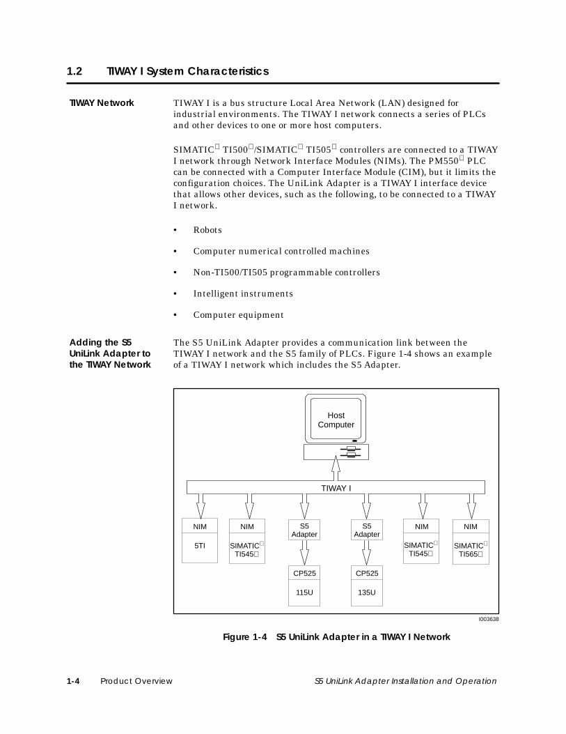
1.2 TIWAY I System Characteristics
TIWAY I is a bus structure Local Area Network (LAN) designed forindustrial environments. The TIWAY I network connects a series of PLCsand other devices to one or more host computers.
SIMATIC TI500 /SIMATIC TI505 controllers are connected to a TIWAYI network through Network Interface Modules (NIMs). The PM550 PLCcan be connected with a Computer Interface Module (CIM), but it limits theconfiguration choices. The UniLink Adapter is a TIWAY I interface devicethat allows other devices, such as the following, to be connected to a TIWAYI network.
• Robots
• Computer numerical controlled machines
• Non-TI500/TI505 programmable controllers
• Intelligent instruments
• Computer equipment
The S5 UniLink Adapter provides a communication link between theTIWAY I network and the S5 family of PLCs. Figure 1-4 shows an exampleof a TIWAY I network which includes the S5 Adapter.
I003638
S5Adapter
NIM
5TI
NIM
SIMATIC
TI545
NIM
SIMATIC
TI545
NIM
SIMATIC
TI565
CP525
135U
CP525
115U
S5Adapter
TIWAY I
HostComputer
Figure 1-4 S5 UniLink Adapter in a TIWAY I Network
TIWAY Network
Adding the S5UniLink Adapter tothe TIWAY Network
Product Overview 1-5S5 UniLink Adapter Installation and Operation
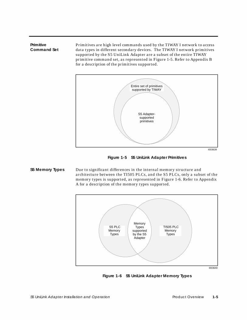
Primitives are high level commands used by the TIWAY I network to accessdata types in different secondary devices. The TIWAY I network primitivessupported by the S5 UniLink Adapter are a subset of the entire TIWAYprimitive command set, as represented in Figure 1-5. Refer to Appendix Bfor a description of the primitives supported.
I003639
S5 Adapter-supportedprimitives
Entire set of primitivessupported by TIWAY
Figure 1-5 S5 UniLink Adapter Primitives
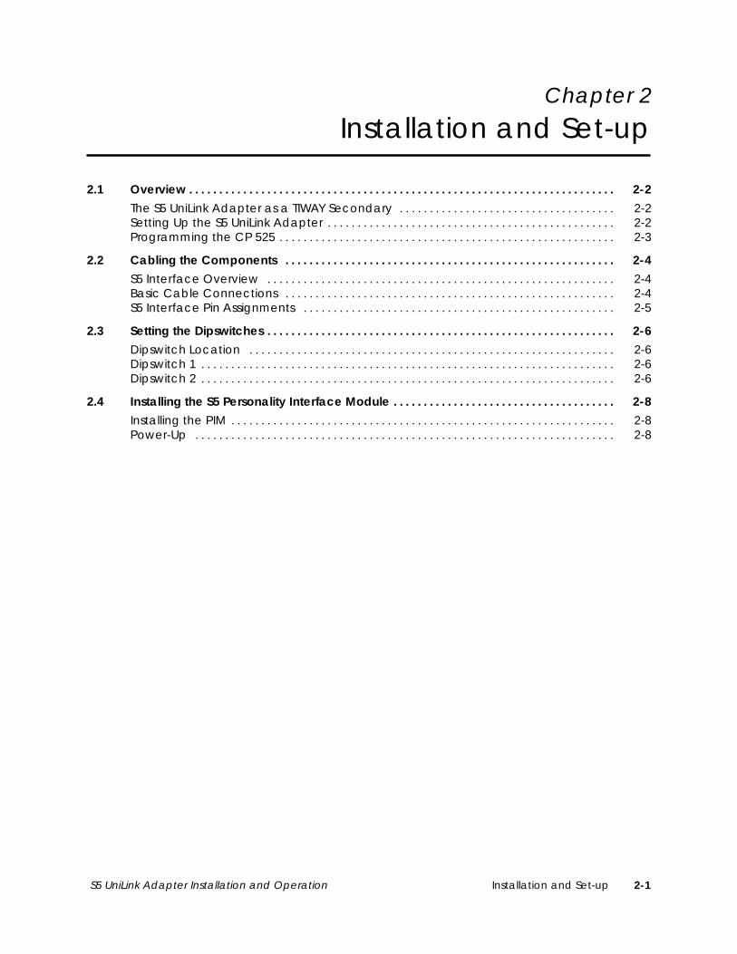
Due to significant differences in the internal memory structure andarchitecture between the TI505 PLCs, and the S5 PLCs, only a subset of thememory types is supported, as represented in Figure 1-6. Refer to AppendixA for a description of the memory types supported.
I003640
S5 PLCMemoryTypes
TI505 PLCMemoryTypes
MemoryTypes
supportedby the S5Adapter
Figure 1-6 S5 UniLink Adapter Memory Types
PrimitiveCommand Set
S5 Memory Types
Installation and Set-up 2-1S5 UniLink Adapter Installation and Operation
Chapter 2
Installation and Set-up
2.1 Overview 2-2. . . . . . . . . . . . . . . . . . . . . . . . . . . . . . . . . . . . . . . . . . . . . . . . . . . . . . . . . . . . . . . . . . . . . . . The S5 UniLink Adapter as a TIWAY Secondary 2-2. . . . . . . . . . . . . . . . . . . . . . . . . . . . . . . . . . . . Setting Up the S5 UniLink Adapter 2-2. . . . . . . . . . . . . . . . . . . . . . . . . . . . . . . . . . . . . . . . . . . . . . . . Programming the CP 525 2-3. . . . . . . . . . . . . . . . . . . . . . . . . . . . . . . . . . . . . . . . . . . . . . . . . . . . . . . .
2.2 Cabling the Components 2-4. . . . . . . . . . . . . . . . . . . . . . . . . . . . . . . . . . . . . . . . . . . . . . . . . . . . . . . S5 Interface Overview 2-4. . . . . . . . . . . . . . . . . . . . . . . . . . . . . . . . . . . . . . . . . . . . . . . . . . . . . . . . . . Basic Cable Connections 2-4. . . . . . . . . . . . . . . . . . . . . . . . . . . . . . . . . . . . . . . . . . . . . . . . . . . . . . . S5 Interface Pin Assignments 2-5. . . . . . . . . . . . . . . . . . . . . . . . . . . . . . . . . . . . . . . . . . . . . . . . . . . .
2.3 Setting the Dipswitches 2-6. . . . . . . . . . . . . . . . . . . . . . . . . . . . . . . . . . . . . . . . . . . . . . . . . . . . . . . . . . Dipswitch Location 2-6. . . . . . . . . . . . . . . . . . . . . . . . . . . . . . . . . . . . . . . . . . . . . . . . . . . . . . . . . . . . . Dipswitch 1 2-6. . . . . . . . . . . . . . . . . . . . . . . . . . . . . . . . . . . . . . . . . . . . . . . . . . . . . . . . . . . . . . . . . . . . . Dipswitch 2 2-6. . . . . . . . . . . . . . . . . . . . . . . . . . . . . . . . . . . . . . . . . . . . . . . . . . . . . . . . . . . . . . . . . . . . .
2.4 Installing the S5 Personality Interface Module 2-8. . . . . . . . . . . . . . . . . . . . . . . . . . . . . . . . . . . . . Installing the PIM 2-8. . . . . . . . . . . . . . . . . . . . . . . . . . . . . . . . . . . . . . . . . . . . . . . . . . . . . . . . . . . . . . . . Power-Up 2-8. . . . . . . . . . . . . . . . . . . . . . . . . . . . . . . . . . . . . . . . . . . . . . . . . . . . . . . . . . . . . . . . . . . . . .
Installation and Set-up2-2 S5 UniLink Adapter Installation and Operation
2.1 Overview
This chapter provides an introduction to the operation and set-up of theS5 UniLink Adapter.
During normal operation, requests are sent over the TIWAY network to theS5 UniLink Adapter; thus it functions in the same manner as any othersecondary in the network. Appendix B lists the TIWAY primitives supportedby the S5 Adapter.
The majority of requests issued to the S5 Adapter are to obtain memorylocations from the S5 PLC. Appendix A lists the memory translations fromthe TI505 (TT types) to the S5 memory types.
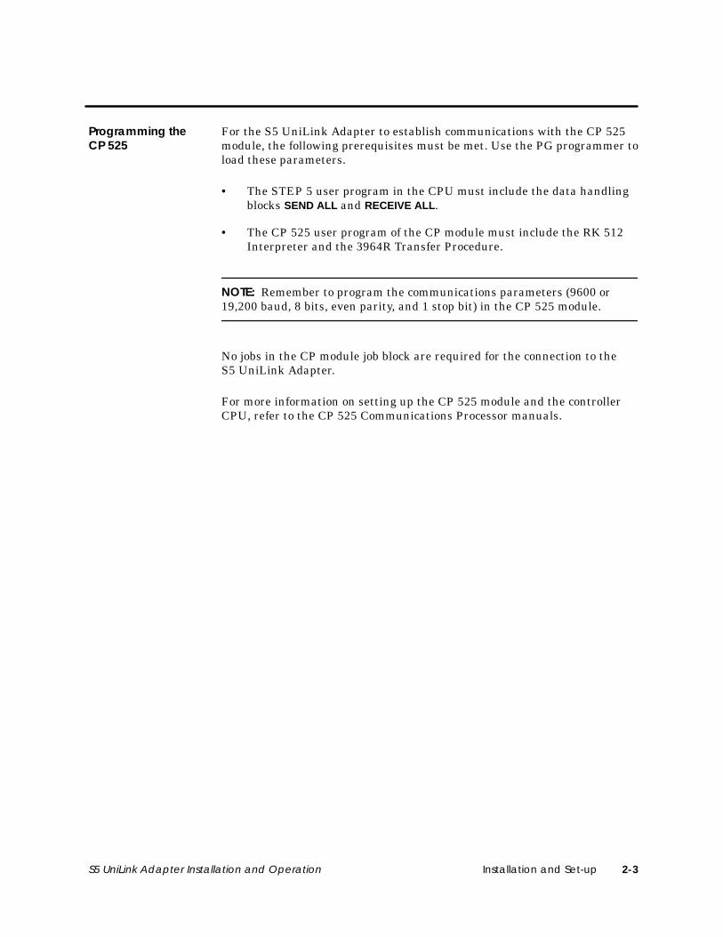
To connect and set up the S5 UniLink Adapter properly, follow these steps.
Run appropriate cabling.
Program the CP 525 Communications Processor and the S5 PLC CPU.
Set the Dipswitches in the S5 UniLink Adapter.
Install the S5 Personality Interface Module (PIM).
Power Up the S5 UniLink Adapter.
Figure 2-1 Main Steps for Setting up the S5 UniLink Adapter
The S5 UniLinkAdapter as a TIWAYSecondary
Setting Up theS5 UniLink Adapter
Installation and Set-up 2-3S5 UniLink Adapter Installation and Operation
For the S5 UniLink Adapter to establish communications with the CP 525module, the following prerequisites must be met. Use the PG programmer toload these parameters.
• The STEP 5 user program in the CPU must include the data handlingblocks SEND ALL and RECEIVE ALL.
• The CP 525 user program of the CP module must include the RK 512Interpreter and the 3964R Transfer Procedure.
NOTE: Remember to program the communications parameters (9600 or19,200 baud, 8 bits, even parity, and 1 stop bit) in the CP 525 module.
No jobs in the CP module job block are required for the connection to theS5 UniLink Adapter.
For more information on setting up the CP 525 module and the controllerCPU, refer to the CP 525 Communications Processor manuals.
Programming theCP 525
Installation and Set-up2-4 S5 UniLink Adapter Installation and Operation
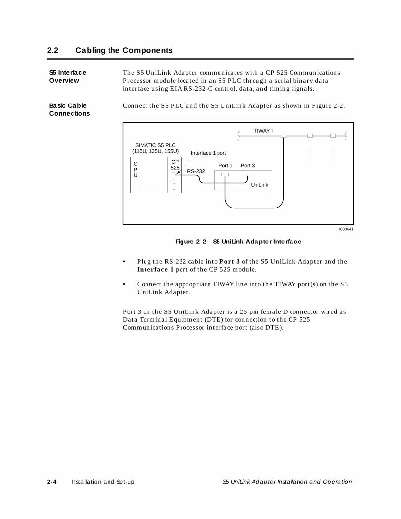
2.2 Cabling the Components
The S5 UniLink Adapter communicates with a CP 525 CommunicationsProcessor module located in an S5 PLC through a serial binary datainterface using EIA RS-232-C control, data, and timing signals.
Connect the S5 PLC and the S5 UniLink Adapter as shown in Figure 2-2.
I003641
SIMATIC S5 PLC(115U, 135U, 155U)
CP525
RS-232CPU
Port 1 Port 3
TIWAY I
UniLink
Interface 1 port
Figure 2-2 S5 UniLink Adapter Interface
• Plug the RS-232 cable into Port 3 of the S5 UniLink Adapter and theInterface 1 port of the CP 525 module.
• Connect the appropriate TIWAY line into the TIWAY port(s) on the S5UniLink Adapter.
Port 3 on the S5 UniLink Adapter is a 25-pin female D connector wired asData Terminal Equipment (DTE) for connection to the CP 525Communications Processor interface port (also DTE).
S5 InterfaceOverview
Basic CableConnections
Installation and Set-up 2-5S5 UniLink Adapter Installation and Operation
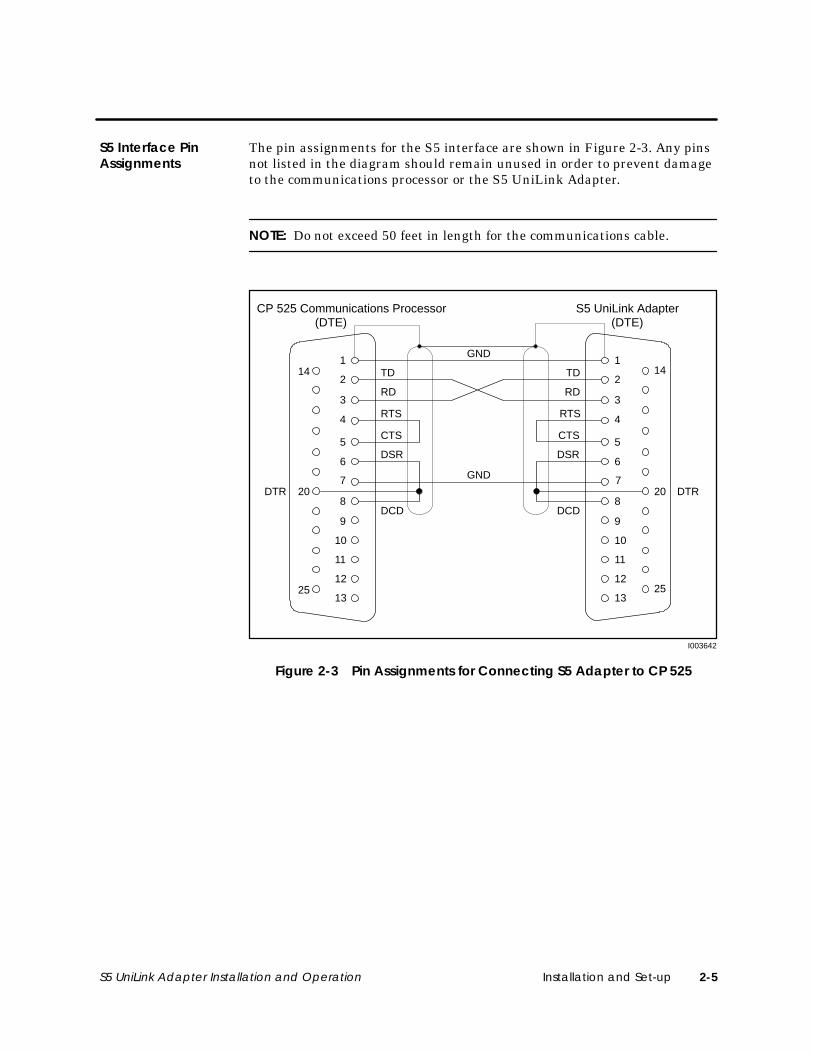
The pin assignments for the S5 interface are shown in Figure 2-3. Any pinsnot listed in the diagram should remain unused in order to prevent damageto the communications processor or the S5 UniLink Adapter.
NOTE: Do not exceed 50 feet in length for the communications cable.
1
2
3
4
5
6
208
7
1
2
3
4
5
6
208
7
(DTE) (DTE)
GND
9 9
10 10
11 11
12 12
13 13
CP 525 Communications Processor S5 UniLink Adapter
14 14TD TD
RD RD
RTS RTS
CTS CTS
GND
DSR
DCD
DSR
DCD
25 25
DTR DTR
I003642
Figure 2-3 Pin Assignments for Connecting S5 Adapter to CP 525
S5 Interface PinAssignments
Installation and Set-up2-6 S5 UniLink Adapter Installation and Operation
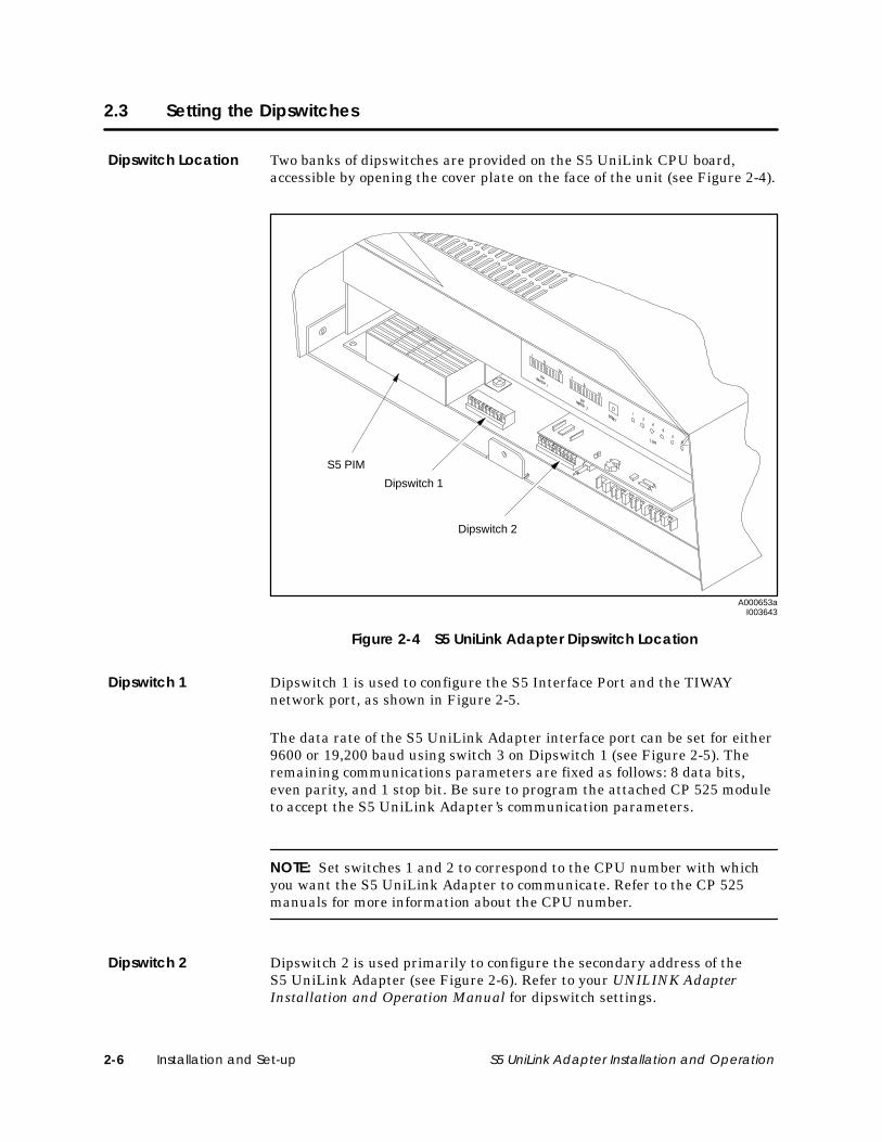
2.3 Setting the Dipswitches
Two banks of dipswitches are provided on the S5 UniLink CPU board,accessible by opening the cover plate on the face of the unit (see Figure 2-4).
A000653a
S5 PIM
Dipswitch 1
Dipswitch 2
I003643
Figure 2-4 S5 UniLink Adapter Dipswitch Location
Dipswitch 1 is used to configure the S5 Interface Port and the TIWAYnetwork port, as shown in Figure 2-5.
The data rate of the S5 UniLink Adapter interface port can be set for either9600 or 19,200 baud using switch 3 on Dipswitch 1 (see Figure 2-5). Theremaining communications parameters are fixed as follows: 8 data bits,even parity, and 1 stop bit. Be sure to program the attached CP 525 moduleto accept the S5 UniLink Adapter’s communication parameters.
NOTE: Set switches 1 and 2 to correspond to the CPU number with whichyou want the S5 UniLink Adapter to communicate. Refer to the CP 525manuals for more information about the CPU number.
Dipswitch 2 is used primarily to configure the secondary address of theS5 UniLink Adapter (see Figure 2-6). Refer to your UNILINK AdapterInstallation and Operation Manual for dipswitch settings.
Dipswitch Location
Dipswitch 1
Dipswitch 2
Installation and Set-up 2-7S5 UniLink Adapter Installation and Operation
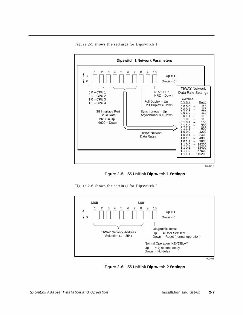
Figure 2-5 shows the settings for Dipswitch 1.
I003644
TIWAY NetworkData Rates
Up = 1
Down = 0
Dipswitch 1 Network Parameters
TIWAY NetworkData Rate Settings
0 0 0 0 – 1100 0 0 1 – 1100 0 1 0 – 1100 0 1 1 – 1100 1 0 0 – 1100 1 0 1 – 1500 1 1 0 – 3000 1 1 1 – 6001 0 0 0 – 12001 0 0 1 – 24001 0 1 0 – 48001 0 1 1 – 96001 1 0 0 – 192001 1 0 1 – 384001 1 1 0 – 576001 1 1 1 – 115200
Switches4 5 6 7 Baud
1 2 3 4 5 6 7 8 9 10
0 0 – CPU 10 1 – CPU 21 0 – CPU 31 1 – CPU 4
NRZI = UpNRZ = Down
Full Duplex = UpHalf Duplex = Down
Synchronous = UpAsynchronous = Down
19200 = Up9600 = Down
S5 Interface PortBaud Rate
1
0
Figure 2-5 S5 UniLink Dipswitch 1 Settings
Figure 2-6 shows the settings for Dipswitch 2.
I003645
Up = 1
Down = 0
1 2 3 4 5 6 7 8 9 10
Diagnostic Tests:Up = User Self TestDown = Reset (normal operation)
1
0
TIWAY Network AddressSelection (1 – 254)
Normal Operation: KEYDELAYUp = 1 �2 second delayDown = No delay
MSB LSB
Figure 2-6 S5 UniLink Dipswitch 2 Settings
Installation and Set-up2-8 S5 UniLink Adapter Installation and Operation
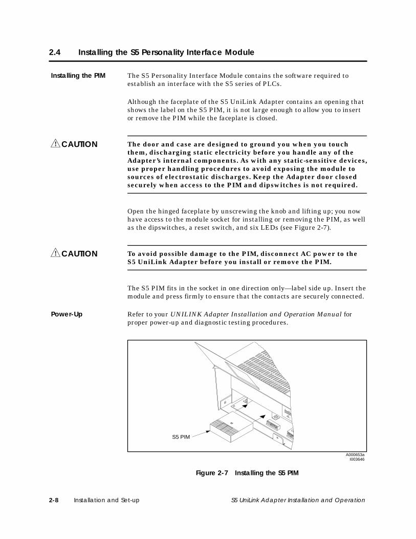
2.4 Installing the S5 Personality Interface Module
The S5 Personality Interface Module contains the software required toestablish an interface with the S5 series of PLCs.
Although the faceplate of the S5 UniLink Adapter contains an opening thatshows the label on the S5 PIM, it is not large enough to allow you to insertor remove the PIM while the faceplate is closed.
The door and case are designed to ground you when you touchthem, discharging static electricity before you handle any of theAdapter’s internal components. As with any static-sensitive devices,use proper handling procedures to avoid exposing the module tosources of electrostatic discharges. Keep the Adapter door closedsecurely when access to the PIM and dipswitches is not required.
Open the hinged faceplate by unscrewing the knob and lifting up; you nowhave access to the module socket for installing or removing the PIM, as wellas the dipswitches, a reset switch, and six LEDs (see Figure 2-7).
To avoid possible damage to the PIM, disconnect AC power to theS5 UniLink Adapter before you install or remove the PIM.
The S5 PIM fits in the socket in one direction only—label side up. Insert themodule and press firmly to ensure that the contacts are securely connected.
Refer to your UNILINK Adapter Installation and Operation Manual forproper power-up and diagnostic testing procedures.
A000653aI003646
S5 PIM
Figure 2-7 Installing the S5 PIM
Installing the PIM
CAUTION!
CAUTION!
Power-Up
TIWAY I Network Communication 3-1S5 UniLink Adapter Installation and Operation
Chapter 3
TIWAY I Network Communication
3.1 Local Line Interface Ports 3-2. . . . . . . . . . . . . . . . . . . . . . . . . . . . . . . . . . . . . . . . . . . . . . . . . . . . . . . . Overview 3-2. . . . . . . . . . . . . . . . . . . . . . . . . . . . . . . . . . . . . . . . . . . . . . . . . . . . . . . . . . . . . . . . . . . . . . . Local Line Interface Ports 3-2. . . . . . . . . . . . . . . . . . . . . . . . . . . . . . . . . . . . . . . . . . . . . . . . . . . . . . . . Local Line Pin Assignments 3-3. . . . . . . . . . . . . . . . . . . . . . . . . . . . . . . . . . . . . . . . . . . . . . . . . . . . . . Local Line Bus Structure 3-3. . . . . . . . . . . . . . . . . . . . . . . . . . . . . . . . . . . . . . . . . . . . . . . . . . . . . . . . . Local Line Data Transmission Parameters 3-4. . . . . . . . . . . . . . . . . . . . . . . . . . . . . . . . . . . . . . . . .
3.2 Modem Interface Ports 3-5. . . . . . . . . . . . . . . . . . . . . . . . . . . . . . . . . . . . . . . . . . . . . . . . . . . . . . . . . . RS-232-C Modem Interface Ports 3-5. . . . . . . . . . . . . . . . . . . . . . . . . . . . . . . . . . . . . . . . . . . . . . . . Modem Port Pin Assignments 3-5. . . . . . . . . . . . . . . . . . . . . . . . . . . . . . . . . . . . . . . . . . . . . . . . . . . . Modem Specifications 3-6. . . . . . . . . . . . . . . . . . . . . . . . . . . . . . . . . . . . . . . . . . . . . . . . . . . . . . . . . . Runaway Transmitter Recovery 3-6. . . . . . . . . . . . . . . . . . . . . . . . . . . . . . . . . . . . . . . . . . . . . . . . . .
3.3 Redundant Media Transmission 3-7. . . . . . . . . . . . . . . . . . . . . . . . . . . . . . . . . . . . . . . . . . . . . . . . . . Alternate Channel Port 3-7. . . . . . . . . . . . . . . . . . . . . . . . . . . . . . . . . . . . . . . . . . . . . . . . . . . . . . . . .
3.4 TIWAY I HDLC Network Protocol 3-8. . . . . . . . . . . . . . . . . . . . . . . . . . . . . . . . . . . . . . . . . . . . . . . . . .
3.5 S5 Interface Port Communications 3-9. . . . . . . . . . . . . . . . . . . . . . . . . . . . . . . . . . . . . . . . . . . . . . . Overview 3-9. . . . . . . . . . . . . . . . . . . . . . . . . . . . . . . . . . . . . . . . . . . . . . . . . . . . . . . . . . . . . . . . . . . . . . . S5 Interface Communications 3-9. . . . . . . . . . . . . . . . . . . . . . . . . . . . . . . . . . . . . . . . . . . . . . . . . . . RK 512 Computer Link with 3964R Procedure 3-9. . . . . . . . . . . . . . . . . . . . . . . . . . . . . . . . . . . . .
3.6 Transmitting with the 3964R Procedure 3-10. . . . . . . . . . . . . . . . . . . . . . . . . . . . . . . . . . . . . . . . . . . . Link Establishment 3-10. . . . . . . . . . . . . . . . . . . . . . . . . . . . . . . . . . . . . . . . . . . . . . . . . . . . . . . . . . . . . . . Transmission 3-10. . . . . . . . . . . . . . . . . . . . . . . . . . . . . . . . . . . . . . . . . . . . . . . . . . . . . . . . . . . . . . . . . . . . Acknowledgment 3-10. . . . . . . . . . . . . . . . . . . . . . . . . . . . . . . . . . . . . . . . . . . . . . . . . . . . . . . . . . . . . .
3.7 Receiving with the 3964R Procedure 3-11. . . . . . . . . . . . . . . . . . . . . . . . . . . . . . . . . . . . . . . . . . . . . Link Establishment 3-11. . . . . . . . . . . . . . . . . . . . . . . . . . . . . . . . . . . . . . . . . . . . . . . . . . . . . . . . . . . . . . . Receiving 3-11. . . . . . . . . . . . . . . . . . . . . . . . . . . . . . . . . . . . . . . . . . . . . . . . . . . . . . . . . . . . . . . . . . . . . . Initialization Conflict 3-11. . . . . . . . . . . . . . . . . . . . . . . . . . . . . . . . . . . . . . . . . . . . . . . . . . . . . . . . . . . . . Longitudinal Parity (BCC Comparison) 3-12. . . . . . . . . . . . . . . . . . . . . . . . . . . . . . . . . . . . . . . . . . . For Additional Information 3-12. . . . . . . . . . . . . . . . . . . . . . . . . . . . . . . . . . . . . . . . . . . . . . . . . . . . . . .
TIWAY I Network Communication3-2 S5 UniLink Adapter Installation and Operation
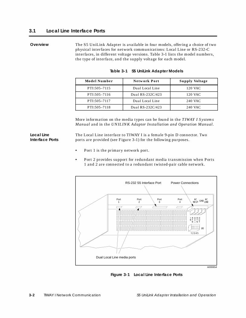
3.1 Local Line Interface Ports
The S5 UniLink Adapter is available in four models, offering a choice of twophysical interfaces for network communications: Local Line or RS-232-Cinterfaces, in different voltage versions. Table 3-1 lists the model numbers,the type of interface, and the supply voltage for each model.
Table 3-1 S5 UniLink Adapter Models
Model Number Network Port Supply Voltage
PTI:505–7115 Dual Local Line 120 VAC
PTI:505–7116 Dual RS-232C/423 120 VAC
PTI:505–7117 Dual Local Line 240 VAC
PTI:505–7118 Dual RS-232C/423 240 VAC
More information on the media types can be found in the TIWAY I SystemsManual and in the UNILINK Adapter Installation and Operation Manual.
The Local Line interface to TIWAY I is a female 9-pin D connector. Twoports are provided (see Figure 3-1) for the following purposes.
• Port 1 is the primary network port.
• Port 2 provides support for redundant media transmission when Ports1 and 2 are connected to a redundant twisted-pair cable network.
A000654
Port1
Port2
Port3
Port4
ACNEUT
ACLINEGND
1 2 3 4 5
I/O
RS-232 S5 Interface Port Power Connections
Dual Local Line media ports
Figure 3-1 Local Line Interface Ports
Overview
Local LineInterface Ports
TIWAY I Network Communication 3-3S5 UniLink Adapter Installation and Operation
The pin assignments for these ports are listed in Table 3-2.
Table 3-2 Local Line Connector Pin Assignments
Pin Name Description
123456789
Shield
LLM+
LLM–
ReservedReservedCable shield and signal commonReservedReservedPositive biased signal lineReservedReservedNegative biased signal line
The Local Line interface uses shielded, twisted-pair cable, such as Belden 9860 or Belden 9271.
Figure 3-2 shows the TIWAY I bus structure with the network trunklinecable, which can extend up to 25,000 feet with droplines up to 100 feet inlength.
I003647
SIMATICS5 PLC
CP525
RS-232 S5 Interface Cable
TIWAY I Main Trunkline
UniLink
Series 500PLC
Series 505PLC
100 ft max.
25,000 feet max.
Figure 3-2 TIWAY I Bus Structure
Local Line PinAssignments
Local Line BusStructure
TIWAY I Network Communication3-4 S5 UniLink Adapter Installation and Operation
Local Line Interface Ports (continued)
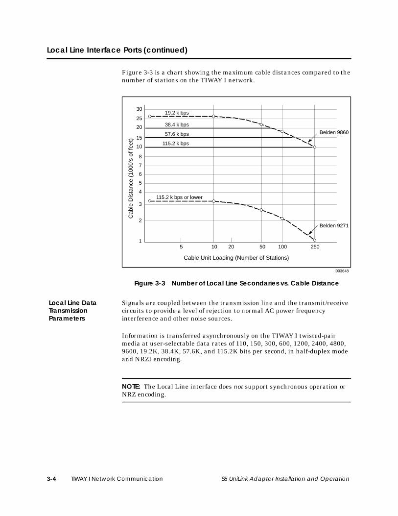
Figure 3-3 is a chart showing the maximum cable distances compared to thenumber of stations on the TIWAY I network.
30
25
20
15
10
8
5
4
3
2
1
6
7
10 50 100 250
Cable Unit Loading (Number of Stations)
19.2 k bps
38.4 k bps
57.6 k bps
115.2 k bps
115.2 k bps or lower
Belden 9860
Belden 9271
Cab
le D
ista
nce
(100
0’s
of fe
et)
205
I003648
Figure 3-3 Number of Local Line Secondaries vs. Cable Distance
Signals are coupled between the transmission line and the transmit/receivecircuits to provide a level of rejection to normal AC power frequencyinterference and other noise sources.
Information is transferred asynchronously on the TIWAY I twisted-pairmedia at user-selectable data rates of 110, 150, 300, 600, 1200, 2400, 4800,9600, 19.2K, 38.4K, 57.6K, and 115.2K bits per second, in half-duplex modeand NRZI encoding.
NOTE: The Local Line interface does not support synchronous operation orNRZ encoding.
Local Line DataTransmissionParameters
TIWAY I Network Communication 3-5S5 UniLink Adapter Installation and Operation
3.2 Modem Interface Ports
The modem interface is a standard Type E DTE configuration as defined inthe EIA RS-232-C standard that uses EIA RS-423 drivers. This interfaceuses a female 25-pin D-type connector on both Ports 1 and 2 as shown inFigure 3-4.
A000654
Port1
Port2
Port3
Port4
ACNEUT
ACLINEGND
1 2 3 4 5
I/O
RS-232 S5 Interface Port Power Connections
Dual RS-232 modem interface ports
Figure 3-4 RS-232/RS-423 Modem Interface Ports
These two ports support redundant media transmission when connected toredundant modem networks. The pin assignments shown in Table 3-3 aresupported. All other pins should be left vacant to prevent damage whichmay be caused by nonstandard pin usage.
Table 3-3 RS-232/RS-423 D Connector Pin Assignments
Pin No. CCITT Circuit Description
1 101 AA Protective Ground
7 102 AB Signal Ground
2 103 BA Transmit Data
3 104 BB Receive Data
4 105 CA Request to Send (RTS)
5 106 CB Clear to Send (CTS)
6 107 CC Data Set Ready (DSR)
20 108/2 CD Data Terminal Ready (DTR)
8 109 CF Data Carrier Detect (DCD)
15 114 DB Transmitter Signal Element Timing
17 115 DD Receiver Signal Element Timing
RS-232-C ModemInterface Ports
Modem PortPin Assignments
TIWAY I Network Communication3-6 S5 UniLink Adapter Installation and Operation
Modem Interface Ports (continued)
The line drivers and receivers meet the requirements for the RS-423 andRS-232-C standards. The modem interface is user-selected for eitherasynchronous or synchronous operation at data rates of 110, 150, 300, 600,1200, 2400, 4800, 9600, 19.2K, 38.4K, 57.6K, and 115.2K bits per second.
For communication applications longer than the 25,000 feet limit of theLocal Line interface, you need to use modems.
The modems used must be non-intelligent and have data transparency.Non-intelligent refers to the class of modems that do not have an internalcommand set. Modems such as the Hayes Smartmodem and compatiblesdo have an internal command set and should not be used. (Generally,modems that meet the Bell 103, 202, and 208 specifications will work, butthe Bell 212A class modems will not.) In addition to being non-intelligent,the modems must support data transparency, which means no start bits, nostop bits, and no parity. This is necessary because TIWAY I uses thebit-oriented HDLC protocol to transfer information between devices. Mostshort-haul modems are non-intelligent and provide data transparency.
You also have a choice of using either NRZ or NRZI encoding with themodem interface. NRZI is recommended because of its self-clockingproperties. (Please refer to the appropriate TIWAY documentation forspecific details regarding the use of modems.)
The S5 UniLink Adapter is equipped with a timeout or runaway transmitterrecovery mechanism which ensures that the transmitter does not remainturned on longer that twice the time required to send the maximum lengthmessage. If the transmission exceeds this limit, the Adapter will perform ahardware reset, discarding all macro buffers and any outstandingdirectives.
NOTE: The hardware reset restores the UniLink Adapter to the initializedor power-up state. At this point, the Adapter will have to be reconfiguredand the network restored to its operating state.
ModemSpecifications
RunawayTransmitterRecovery
TIWAY I Network Communication 3-7S5 UniLink Adapter Installation and Operation
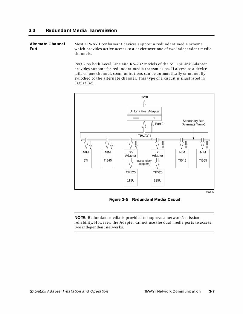
3.3 Redundant Media Transmission
Most TIWAY I conformant devices support a redundant media schemewhich provides active access to a device over one of two independent mediachannels.
Port 2 on both Local Line and RS-232 models of the S5 UniLink Adapterprovides support for redundant media transmission. If access to a devicefails on one channel, communications can be automatically or manuallyswitched to the alternate channel. This type of a circuit is illustrated inFigure 3-5.
I003649
S5Adapter
NIM
5TI
NIM
TI545
NIM
TI545
NIM
TI565
CP525
135U
CP525
115U
S5Adapter
Host
Secondary Bus(Alternate Trunk)
UniLink Host Adapter
TIWAY I
(Secondaryadapters)
Port 2
Figure 3-5 Redundant Media Circuit
NOTE: Redundant media is provided to improve a network’s missionreliability. However, the Adapter cannot use the dual media ports to accesstwo independent networks.
Alternate ChannelPort
TIWAY I Network Communication3-8 S5 UniLink Adapter Installation and Operation
3.4 TIWAY I HDLC Network Protocol
The TIWAY I network uses the HDLC protocol in the unbalanced, normalresponse mode (UNRM) for transmission of commands and responses. Inthis mode, a single Network Manager (primary) controls the flow ofmessages between secondary devices.
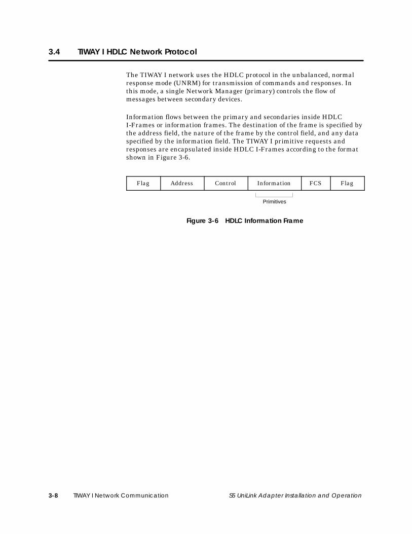
Information flows between the primary and secondaries inside HDLCI-Frames or information frames. The destination of the frame is specified bythe address field, the nature of the frame by the control field, and any dataspecified by the information field. The TIWAY I primitive requests andresponses are encapsulated inside HDLC I-Frames according to the formatshown in Figure 3-6.
Flag Address Control Information FCS Flag
Primitives
Figure 3-6 HDLC Information Frame
TIWAY I Network Communication 3-9S5 UniLink Adapter Installation and Operation
3.5 S5 Interface Port Communications
In automation engineering, data must often be exchanged betweenprogrammable controllers or between a programmable controller and acentral process computer. The data exchange can be implemented using thecommunications processor CP 525 with its interpreter RK 512 and theprocedure 3964R. This means that the programmable controllers of the S5 U family (115U, 135U, 155U) can be hooked up with the S5 UniLinkAdapter through one of these CP modules.
Each S5 UniLink Adapter with an S5 PIM is connected to a CP 525Communications Processor through the S5 interface port with an RS-232interface. The S5 Adapter uses the RK 512 protocol with the 3964R transferprocedure to establish communications with the CP 525 module.
Refer to Chapter 2 for a brief description of the steps necessary to set up theCP 525 Communications Processor.
For more information, consult the CP 525 Communications Processormanuals.
Port 3 on the S5 UniLink Adapter assumes communications with theattached CP 525 module using the 3964R transfer procedure. Sections 3.6and 3.7 discuss the steps involved in transmitting and receiving using the3964R procedure.
Overview
S5 InterfaceCommunications
RK 512 ComputerLink with 3964RProcedure
TIWAY I Network Communication3-10 S5 UniLink Adapter Installation and Operation
3.6 Transmitting with the 3964R Procedure
NOTE: The term procedure refers to the device initiating the transfer, andthe term partner refers to the receiving device.
To establish the link, the procedure sends the control character STX. If thepartner replies within the time allowed of 2000 ms, the procedure starts thetransmission. If the partner answers with NAK, any other character (exceptDLE), or if there is a timeout, then the attempt to establish a link hasfailed. After a total of six unsuccessful attempts, the procedure gives up,signals there is an error establishing the link, and sends the character NAKto the partner.
If the link is successfully established, the information data to be sent to thepartner is immediately sent to the partner at the selected data rate. Thepartner monitors the time between the characters as it receives them. Thetime between two characters must not exceed the character delay time of220 ms.
While the information data is being transmitted, the partner sends thecharacter NAK, the procedure breaks off and repeats it as previouslydescribed. If any other character is received, the procedure waits for thecharacter delay time (220 ms) to elapse and then sends NAK to reset thepartner. Then the procedure begins the transmission again with the linkestablishment STX.
Each DLE character sent is found in the transmission as two DLEcharacters (DLE doubling), i.e., the data (10H) is sent twice.
After sending the information data the procedure adds the characters DLE,ETX, and BCC as end identifier and waits for an acknowledgment.
If the partner sends the character DLE within the time allowed (2000 ms),the information data was received without errors. If the partner replies withany other character (except DLE) or there is a timeout, the procedure beginsthe link establishment again with STX. After a total of six unsuccessfulattempts to send the information data, the procedure breaks off theattempt, signals an error, and sends NAK to the partner.
Link Establishment
Transmission
Acknowledgment
TIWAY I Network Communication 3-11S5 UniLink Adapter Installation and Operation
3.7 Receiving with the 3964R Procedure
After a successful transmission of the data information has been made tothe partner, the procedure enters the idle state awaiting the link to beestablished by the partner. If the procedure receives any character (exceptSTX) while in the idle state, it waits until the character delay time (220 ms)has elapsed and then sends a NAK character. Then a repetition is expected.If after a total of six unsuccessful attempts, or if the repetition by thepartner does not take place within the waiting time of 4 seconds, theprocedure breaks off reception and signals an error.
If the procedure receives the character STX it answers with DLE. Theprocedure now expects a data reception from the partner.
After each character received, the procedure waits for the next character toarrive within the character delay time (220 ms). If there is a charactertimeout, the NAK character is sent to the partner, and a repetition isexpected. If after a total of six unsuccessful attempts, or if the repetition bythe partner does not take place within the waiting time of 4 seconds, theprocedure breaks off reception and signals an error.
If the procedure recognizes the character sequence DLE ETX and BCC, itstops receiving. It compares the received block check character (BCC) withlongitudinal parity. If the block check character is correct and no othererrors have occurred during reception, the procedure sends a DLE. If theBCC does not correspond, NAK is sent to the partner. Then a repetition isexpected. If the block can not be received without errors following sixattempts or if the repetition by the partner does not take place within thewaiting time of 4 seconds, the procedure breaks off and signals an error.
If transmission errors occurs during the reception (characters lost, frameerror, parity error), reception is continued until the link is terminated andthen NAK is sent to the partner. Then a repetition is expected as previouslydescribed.
If a device receives a send request (STX character) from its partner and doesnot answer within the acknowledgment delay time (2000 ms) with DLE orNAK, but also sends the character STX, there is an initialization conflict.Both devices are attempting to perform a send job. The device with thelower priority desists and answers with the DLE character. The device withthe higher priority sends its data as previously described. After the link hasbeen terminated, the lower priority device can then run its send job. The S5UniLink Adapter will assume higher priority, and the CP module should beconfigured with the lower priority.
The CP module will act on a request/response basis, with all requestscoming from the S5 UniLink Adapter. Thus the S5 PLC should beprogrammed never to send any requests through the CP module to theUniLink Adapter. If such a request occurs, the S5 UniLink Adapter willignore the request, causing a timeout to occur.
Link Establishment
Receiving
InitializationConflict
TIWAY I Network Communication3-12 S5 UniLink Adapter Installation and Operation
Receiving with the 3964R Procedure (continued)
The BCC error check byte is calculated by an exclusive-OR of all data bytescontained in the message. The terminating characters DLE and ETX arealso included in the BCC calculation.
For more detailed information concerning the RK 512 protocol and 3964Rtransfer procedure, as well as available commands, please refer to themanuals shipped with your CP 525 module.
Longitudinal Parity(BCC Comparison)
For AdditionalInformation
Simatic S5 Memory Mapping A-1S5 UniLink Adapter Installation and Operation
Appendix A
SIMATIC S5 Memory Mapping
A.1 Memory Type Overview A-2. . . . . . . . . . . . . . . . . . . . . . . . . . . . . . . . . . . . . . . . . . . . . . . . . . . . . . . . . Overview A-2. . . . . . . . . . . . . . . . . . . . . . . . . . . . . . . . . . . . . . . . . . . . . . . . . . . . . . . . . . . . . . . . . . . . . . . Quick Reference Memory Chart A-2. . . . . . . . . . . . . . . . . . . . . . . . . . . . . . . . . . . . . . . . . . . . . . . . .
A.2 Floating-Point Conversion A-3. . . . . . . . . . . . . . . . . . . . . . . . . . . . . . . . . . . . . . . . . . . . . . . . . . . . . . . Description A-3. . . . . . . . . . . . . . . . . . . . . . . . . . . . . . . . . . . . . . . . . . . . . . . . . . . . . . . . . . . . . . . . . . . . .
A.3 Data Block — CP 525 ‘D’ Type A-4. . . . . . . . . . . . . . . . . . . . . . . . . . . . . . . . . . . . . . . . . . . . . . . . . . . Description A-4. . . . . . . . . . . . . . . . . . . . . . . . . . . . . . . . . . . . . . . . . . . . . . . . . . . . . . . . . . . . . . . . . . . . . Address Mapping A-4. . . . . . . . . . . . . . . . . . . . . . . . . . . . . . . . . . . . . . . . . . . . . . . . . . . . . . . . . . . . . . . Value Conversion A-4. . . . . . . . . . . . . . . . . . . . . . . . . . . . . . . . . . . . . . . . . . . . . . . . . . . . . . . . . . . . . . . Floating-Point Support A-4. . . . . . . . . . . . . . . . . . . . . . . . . . . . . . . . . . . . . . . . . . . . . . . . . . . . . . . . . . . Reading and Writing A-4. . . . . . . . . . . . . . . . . . . . . . . . . . . . . . . . . . . . . . . . . . . . . . . . . . . . . . . . . . . .
A.4 Extended Data Block — CP 525 ‘X’ Type A-5. . . . . . . . . . . . . . . . . . . . . . . . . . . . . . . . . . . . . . . . . . Description A-5. . . . . . . . . . . . . . . . . . . . . . . . . . . . . . . . . . . . . . . . . . . . . . . . . . . . . . . . . . . . . . . . . . . . . Address Mapping A-5. . . . . . . . . . . . . . . . . . . . . . . . . . . . . . . . . . . . . . . . . . . . . . . . . . . . . . . . . . . . . . . Value Conversion A-5. . . . . . . . . . . . . . . . . . . . . . . . . . . . . . . . . . . . . . . . . . . . . . . . . . . . . . . . . . . . . . . Floating-Point Support A-5. . . . . . . . . . . . . . . . . . . . . . . . . . . . . . . . . . . . . . . . . . . . . . . . . . . . . . . . . . . Reading and Writing A-5. . . . . . . . . . . . . . . . . . . . . . . . . . . . . . . . . . . . . . . . . . . . . . . . . . . . . . . . . . . .
A.5 Input Bytes — CP 525 ‘E’ Type A-6. . . . . . . . . . . . . . . . . . . . . . . . . . . . . . . . . . . . . . . . . . . . . . . . . . . . Description A-6. . . . . . . . . . . . . . . . . . . . . . . . . . . . . . . . . . . . . . . . . . . . . . . . . . . . . . . . . . . . . . . . . . . . . Address Mapping A-6. . . . . . . . . . . . . . . . . . . . . . . . . . . . . . . . . . . . . . . . . . . . . . . . . . . . . . . . . . . . . . . Value Conversion A-6. . . . . . . . . . . . . . . . . . . . . . . . . . . . . . . . . . . . . . . . . . . . . . . . . . . . . . . . . . . . . . . Reading and Writing A-6. . . . . . . . . . . . . . . . . . . . . . . . . . . . . . . . . . . . . . . . . . . . . . . . . . . . . . . . . . . .
A.6 Output Bytes — CP 525 ‘A’ Type A-7. . . . . . . . . . . . . . . . . . . . . . . . . . . . . . . . . . . . . . . . . . . . . . . . . . Description A-7. . . . . . . . . . . . . . . . . . . . . . . . . . . . . . . . . . . . . . . . . . . . . . . . . . . . . . . . . . . . . . . . . . . . . Address Mapping A-7. . . . . . . . . . . . . . . . . . . . . . . . . . . . . . . . . . . . . . . . . . . . . . . . . . . . . . . . . . . . . . . Value Conversion A-7. . . . . . . . . . . . . . . . . . . . . . . . . . . . . . . . . . . . . . . . . . . . . . . . . . . . . . . . . . . . . . . Reading and Writing A-7. . . . . . . . . . . . . . . . . . . . . . . . . . . . . . . . . . . . . . . . . . . . . . . . . . . . . . . . . . . .
A.7 Flag Bytes — CP 525 ‘M’ Type A-8. . . . . . . . . . . . . . . . . . . . . . . . . . . . . . . . . . . . . . . . . . . . . . . . . . . . Description A-8. . . . . . . . . . . . . . . . . . . . . . . . . . . . . . . . . . . . . . . . . . . . . . . . . . . . . . . . . . . . . . . . . . . . . Address Mapping A-8. . . . . . . . . . . . . . . . . . . . . . . . . . . . . . . . . . . . . . . . . . . . . . . . . . . . . . . . . . . . . . . Value Conversion A-8. . . . . . . . . . . . . . . . . . . . . . . . . . . . . . . . . . . . . . . . . . . . . . . . . . . . . . . . . . . . . . . Reading and Writing A-8. . . . . . . . . . . . . . . . . . . . . . . . . . . . . . . . . . . . . . . . . . . . . . . . . . . . . . . . . . . .
A.8 Timer — CP 525 ‘T’ Type A-9. . . . . . . . . . . . . . . . . . . . . . . . . . . . . . . . . . . . . . . . . . . . . . . . . . . . . . . . . Description A-9. . . . . . . . . . . . . . . . . . . . . . . . . . . . . . . . . . . . . . . . . . . . . . . . . . . . . . . . . . . . . . . . . . . . . Address Mapping A-9. . . . . . . . . . . . . . . . . . . . . . . . . . . . . . . . . . . . . . . . . . . . . . . . . . . . . . . . . . . . . . . Value Conversion A-9. . . . . . . . . . . . . . . . . . . . . . . . . . . . . . . . . . . . . . . . . . . . . . . . . . . . . . . . . . . . . . . Reading and Writing A-9. . . . . . . . . . . . . . . . . . . . . . . . . . . . . . . . . . . . . . . . . . . . . . . . . . . . . . . . . . . .
A.9 Counter — CP 525 ‘Z’ Type A-10. . . . . . . . . . . . . . . . . . . . . . . . . . . . . . . . . . . . . . . . . . . . . . . . . . . . . . Description A-10. . . . . . . . . . . . . . . . . . . . . . . . . . . . . . . . . . . . . . . . . . . . . . . . . . . . . . . . . . . . . . . . . . . . . Address Mapping A-10. . . . . . . . . . . . . . . . . . . . . . . . . . . . . . . . . . . . . . . . . . . . . . . . . . . . . . . . . . . . . . . Value Conversion A-10. . . . . . . . . . . . . . . . . . . . . . . . . . . . . . . . . . . . . . . . . . . . . . . . . . . . . . . . . . . . . . . Reading and Writing A-10. . . . . . . . . . . . . . . . . . . . . . . . . . . . . . . . . . . . . . . . . . . . . . . . . . . . . . . . . . . .
A.10 S5 Data Types Not Supported by S5 PIM A-11. . . . . . . . . . . . . . . . . . . . . . . . . . . . . . . . . . . . . . . . . . Analog I/O Bytes: CP 525 ‘P’ Type A-11. . . . . . . . . . . . . . . . . . . . . . . . . . . . . . . . . . . . . . . . . . . . . . . Extended Analog I/O Bytes: CP 525 ‘Q’ Type A-11. . . . . . . . . . . . . . . . . . . . . . . . . . . . . . . . . . . . . Absolute Address: CP 525 ‘S’ Type A-11. . . . . . . . . . . . . . . . . . . . . . . . . . . . . . . . . . . . . . . . . . . . . . . System Address: CP 525 ‘B’ Type A-11. . . . . . . . . . . . . . . . . . . . . . . . . . . . . . . . . . . . . . . . . . . . . . . . .
Simatic S5 Memory MappingA-2 S5 UniLink Adapter Installation and Operation
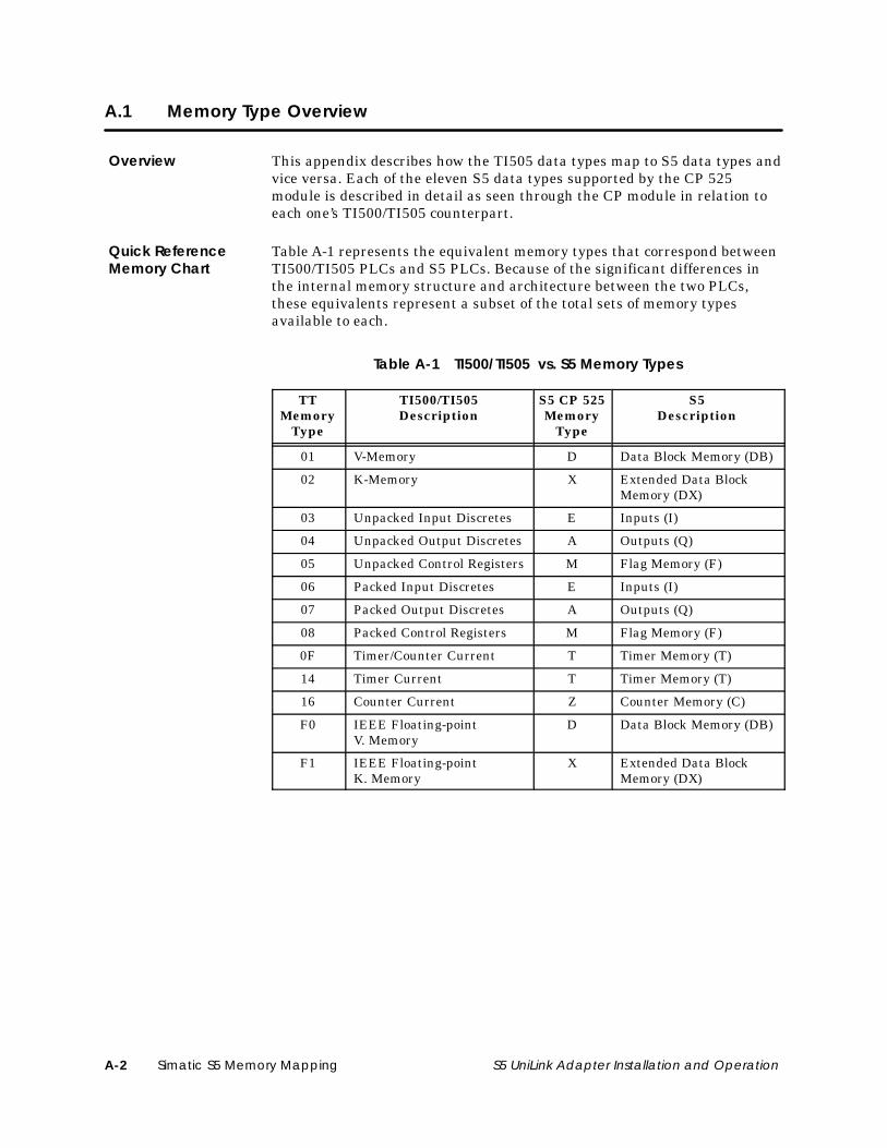
A.1 Memory Type Overview
This appendix describes how the TI505 data types map to S5 data types andvice versa. Each of the eleven S5 data types supported by the CP 525module is described in detail as seen through the CP module in relation toeach one’s TI500/TI505 counterpart.
Table A-1 represents the equivalent memory types that correspond betweenTI500/TI505 PLCs and S5 PLCs. Because of the significant differences inthe internal memory structure and architecture between the two PLCs,these equivalents represent a subset of the total sets of memory typesavailable to each.
Table A-1 TI500/TI505 vs. S5 Memory Types
TTMemory
Type
TI500/TI505Description
S5 CP 525Memory
Type
S5Description
01 V-Memory D Data Block Memory (DB)
02 K-Memory X Extended Data BlockMemory (DX)
03 Unpacked Input Discretes E Inputs (I)
04 Unpacked Output Discretes A Outputs (Q)
05 Unpacked Control Registers M Flag Memory (F)
06 Packed Input Discretes E Inputs (I)
07 Packed Output Discretes A Outputs (Q)
08 Packed Control Registers M Flag Memory (F)
0F Timer/Counter Current T Timer Memory (T)
14 Timer Current T Timer Memory (T)
16 Counter Current Z Counter Memory (C)
F0 IEEE Floating-pointV. Memory
D Data Block Memory (DB)
F1 IEEE Floating-pointK. Memory
X Extended Data BlockMemory (DX)
Overview
Quick ReferenceMemory Chart
Simatic S5 Memory Mapping A-3S5 UniLink Adapter Installation and Operation
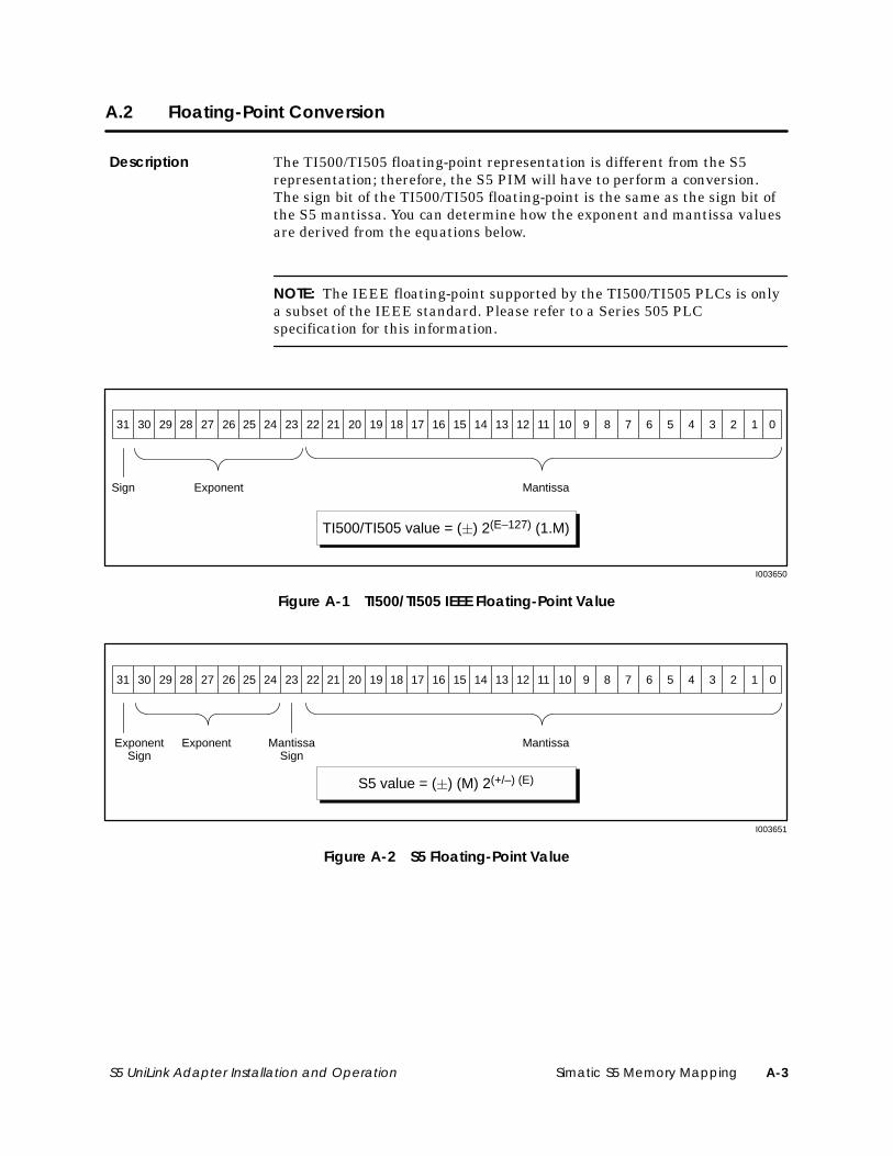
A.2 Floating-Point Conversion
The TI500/TI505 floating-point representation is different from the S5representation; therefore, the S5 PIM will have to perform a conversion.The sign bit of the TI500/TI505 floating-point is the same as the sign bit ofthe S5 mantissa. You can determine how the exponent and mantissa valuesare derived from the equations below.
NOTE: The IEEE floating-point supported by the TI500/TI505 PLCs is onlya subset of the IEEE standard. Please refer to a Series 505 PLCspecification for this information.
31 30 29 28 27 26 25 24 23 22 21 20 19 18 17 16 15 14 13 12 11 10 9 8 7 6 5 4 3 2 1 0
Sign Exponent Mantissa
TI500/TI505 value = (�) 2(E–127) (1.M)
I003650
Figure A-1 TI500/TI505 IEEE Floating-Point Value
31 30 29 28 27 26 25 24 23 22 21 20 19 18 17 16 15 14 13 12 11 10 9 8 7 6 5 4 3 2 1 0
Exponent Mantissa
S5 value = (�) (M) 2(+/–) (E)
MantissaSign
ExponentSign
I003651
Figure A-2 S5 Floating-Point Value
Description
Simatic S5 Memory MappingA-4 S5 UniLink Adapter Installation and Operation
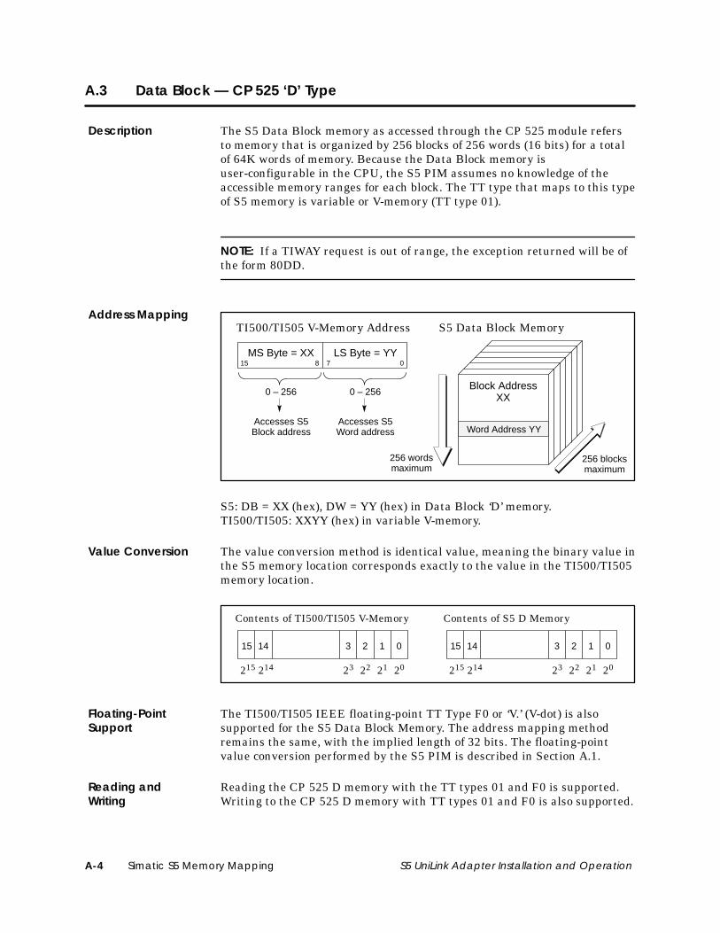
A.3 Data Block — CP 525 ‘D’ Type
The S5 Data Block memory as accessed through the CP 525 module refersto memory that is organized by 256 blocks of 256 words (16 bits) for a totalof 64K words of memory. Because the Data Block memory isuser-configurable in the CPU, the S5 PIM assumes no knowledge of theaccessible memory ranges for each block. The TT type that maps to this typeof S5 memory is variable or V-memory (TT type 01).
NOTE: If a TIWAY request is out of range, the exception returned will be ofthe form 80DD.
S5 Data Block MemoryTI500/TI505 V-Memory Address
MS Byte = XX LS Byte = YY
Block AddressXX
256 wordsmaximum
256 blocksmaximum
Word Address YY
0 – 256
Accesses S5Word address
07
0 – 256
Accesses S5Block address
815
S5: DB = XX (hex), DW = YY (hex) in Data Block ‘D’ memory.TI500/TI505: XXYY (hex) in variable V-memory.
The value conversion method is identical value, meaning the binary value inthe S5 memory location corresponds exactly to the value in the TI500/TI505memory location.
3 2 1 015 14
23 22 21 20215 214
Contents of TI500/TI505 V-Memory
3 2 1 015 14
23 22 21 20215 214
Contents of S5 D Memory
The TI500/TI505 IEEE floating-point TT Type F0 or ‘V.’ (V-dot) is alsosupported for the S5 Data Block Memory. The address mapping methodremains the same, with the implied length of 32 bits. The floating-pointvalue conversion performed by the S5 PIM is described in Section A.1.
Reading the CP 525 D memory with the TT types 01 and F0 is supported.Writing to the CP 525 D memory with TT types 01 and F0 is also supported.
Description
Address Mapping
Value Conversion
Floating-PointSupport
Reading andWriting
Simatic S5 Memory Mapping A-5S5 UniLink Adapter Installation and Operation
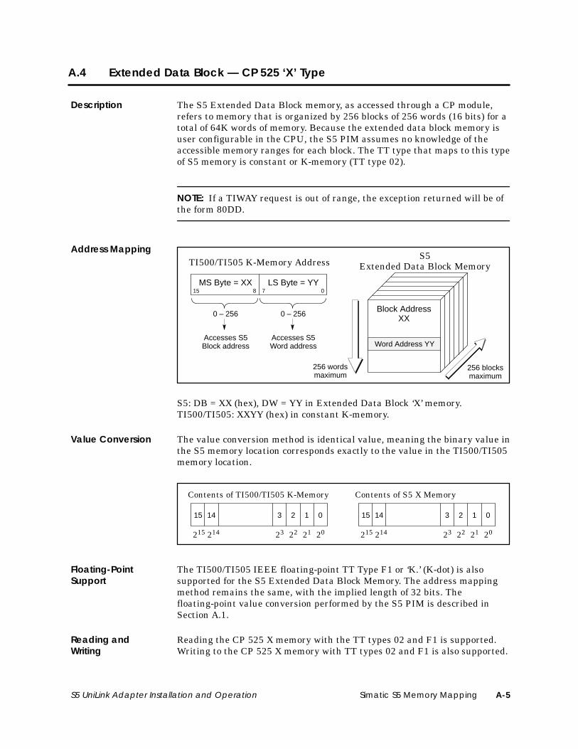
A.4 Extended Data Block — CP 525 ‘X’ Type
The S5 Extended Data Block memory, as accessed through a CP module,refers to memory that is organized by 256 blocks of 256 words (16 bits) for atotal of 64K words of memory. Because the extended data block memory isuser configurable in the CPU, the S5 PIM assumes no knowledge of theaccessible memory ranges for each block. The TT type that maps to this typeof S5 memory is constant or K-memory (TT type 02).
NOTE: If a TIWAY request is out of range, the exception returned will be ofthe form 80DD.
S5Extended Data Block MemoryTI500/TI505 K-Memory Address
MS Byte = XX LS Byte = YY
Block AddressXX
256 wordsmaximum
256 blocksmaximum
Word Address YY
0 – 256
Accesses S5Word address
07
0 – 256
Accesses S5Block address
815
S5: DB = XX (hex), DW = YY in Extended Data Block ‘X’ memory.TI500/TI505: XXYY (hex) in constant K-memory.
The value conversion method is identical value, meaning the binary value inthe S5 memory location corresponds exactly to the value in the TI500/TI505memory location.
3 2 1 015 14
23 22 21 20215 214
Contents of TI500/TI505 K-Memory
3 2 1 015 14
23 22 21 20215 214
Contents of S5 X Memory
The TI500/TI505 IEEE floating-point TT Type F1 or ‘K.’ (K-dot) is alsosupported for the S5 Extended Data Block Memory. The address mappingmethod remains the same, with the implied length of 32 bits. Thefloating-point value conversion performed by the S5 PIM is described inSection A.1.
Reading the CP 525 X memory with the TT types 02 and F1 is supported.Writing to the CP 525 X memory with TT types 02 and F1 is also supported.
Description
Address Mapping
Value Conversion
Floating-PointSupport
Reading andWriting
Simatic S5 Memory MappingA-6 S5 UniLink Adapter Installation and Operation
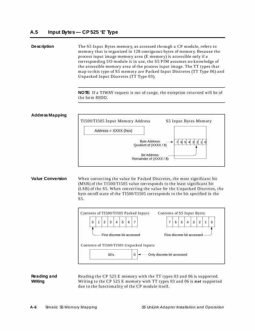
A.5 Input Bytes — CP 525 ‘E’ Type
The S5 Input Bytes memory, as accessed through a CP module, refers tomemory that is organized in 128 contiguous bytes of memory. Because theprocess input image memory area (E memory) is accessible only if acorresponding I/O module is in use, the S5 PIM assumes no knowledge ofthe accessible memory area of the process input image. The TT types thatmap to this type of S5 memory are Packed Input Discretes (TT Type 06) andUnpacked Input Discretes (TT Type 03).
NOTE: If a TIWAY request is out of range, the exception returned will be ofthe form 80DD.
S5 Input Bytes MemoryTI500/TI505 Input Memory Address
Address = XXXX (hex)
3 2 1 07 6 5 4Byte Address:Quotient of (XXXX / 8)
Bit Address:Remainder of (XXXX / 8)
When converting the value for Packed Discretes, the most significant bit(MSB) of the TI500/TI505 value corresponds to the least significant bit(LSB) of the S5. When converting the value for the Unpacked Discretes, thebyte on/off state of the TI500/TI505 corresponds to the bit specified in theS5.
32 6 70 1
Contents of TI500/TI505 Packed Inputs Contents of S5 Input Bytes
4 5 3 267 0145
First discrete bit accessedFirst discrete bit accessed
000’s Only discrete bit accessed
Contents of TI500/TI505 Unpacked Inputs
Reading the CP 525 E memory with the TT types 03 and 06 is supported.Writing to the CP 525 E memory with TT types 03 and 06 is not supporteddue to the functionality of the CP module itself.
Description
Address Mapping
Value Conversion
Reading andWriting
Simatic S5 Memory Mapping A-7S5 UniLink Adapter Installation and Operation
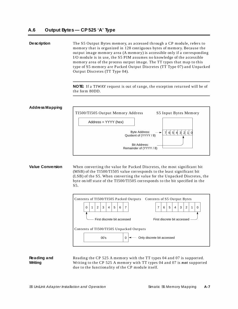
A.6 Output Bytes — CP 525 ‘A’ Type
The S5 Output Bytes memory, as accessed through a CP module, refers tomemory that is organized in 128 contiguous bytes of memory. Because theoutput image memory area (A memory) is accessible only if a correspondingI/O module is in use, the S5 PIM assumes no knowledge of the accessiblememory area of the process output image. The TT types that map to thistype of S5 memory are Packed Output Discretes (TT Type 07) and UnpackedOutput Discretes (TT Type 04).
NOTE: If a TIWAY request is out of range, the exception returned will be ofthe form 80DD.
S5 Input Bytes MemoryTI500/TI505 Output Memory Address
Address = YYYY (hex)
3 2 1 07 6 5 4Byte Address:Quotient of (YYYY / 8)
Bit Address:Remainder of (YYYY / 8)
When converting the value for Packed Discretes, the most significant bit(MSB) of the TI500/TI505 value corresponds to the least significant bit(LSB) of the S5. When converting the value for the Unpacked Discretes, thebyte on/off state of the TI500/TI505 corresponds to the bit specified in theS5.
32 6 70 1
Contents of TI500/TI505 Packed Outputs Contents of S5 Output Bytes
4 5 3 267 0145
First discrete bit accessedFirst discrete bit accessed
000’s Only discrete bit accessed
Contents of TI500/TI505 Unpacked Outputs
Reading the CP 525 A memory with the TT types 04 and 07 is supported.Writing to the CP 525 A memory with TT types 04 and 07 is not supporteddue to the functionality of the CP module itself.
Description
Address Mapping
Value Conversion
Reading andWriting
Simatic S5 Memory MappingA-8 S5 UniLink Adapter Installation and Operation
A.7 Flag Bytes — CP 525 ‘M’ Type
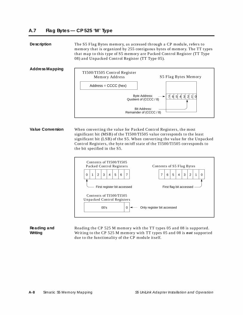
The S5 Flag Bytes memory, as accessed through a CP module, refers tomemory that is organized by 255 contiguous bytes of memory. The TT typesthat map to this type of S5 memory are Packed Control Register (TT Type08) and Unpacked Control Register (TT Type 05).
S5 Flag Bytes MemoryTI500/TI505 Control Register
Memory Address
Address = CCCC (hex)
3 2 1 07 6 5 4Byte Address:Quotient of (CCCC / 8)
Bit Address:Remainder of (CCCC / 8)
When converting the value for Packed Control Registers, the mostsignificant bit (MSB) of the TI500/TI505 value corresponds to the leastsignificant bit (LSB) of the S5. When converting the value for the UnpackedControl Registers, the byte on/off state of the TI500/TI505 corresponds tothe bit specified in the S5.
32 6 70 1
Contents of TI500/TI505Packed Control Registers Contents of S5 Flag Bytes
4 5 3 267 0145
First flag bit accessedFirst register bit accessed
000’s Only register bit accessed
Contents of TI500/TI505Unpacked Control Registers
Reading the CP 525 M memory with the TT types 05 and 08 is supported.Writing to the CP 525 M memory with TT types 05 and 08 is not supporteddue to the functionality of the CP module itself.
Description
Address Mapping
Value Conversion
Reading andWriting
Simatic S5 Memory Mapping A-9S5 UniLink Adapter Installation and Operation
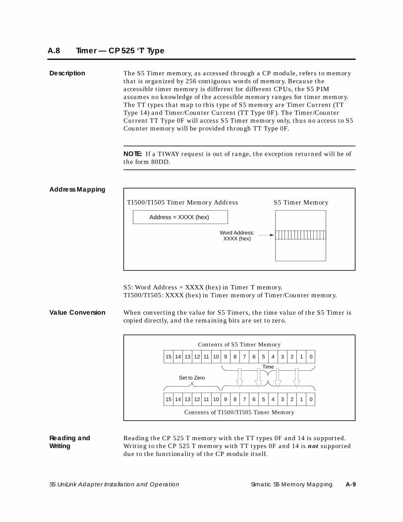
A.8 Timer — CP 525 ‘T’ Type
The S5 Timer memory, as accessed through a CP module, refers to memorythat is organized by 256 contiguous words of memory. Because theaccessible timer memory is different for different CPUs, the S5 PIMassumes no knowledge of the accessible memory ranges for timer memory.The TT types that map to this type of S5 memory are Timer Current (TTType 14) and Timer/Counter Current (TT Type 0F). The Timer/CounterCurrent TT Type 0F will access S5 Timer memory only, thus no access to S5Counter memory will be provided through TT Type 0F.
NOTE: If a TIWAY request is out of range, the exception returned will be ofthe form 80DD.
S5 Timer MemoryTI500/TI505 Timer Memory Address
Address = XXXX (hex)
Word Address:XXXX (hex)
S5: Word Address = XXXX (hex) in Timer T memory.TI500/TI505: XXXX (hex) in Timer memory of Timer/Counter memory.
When converting the value for S5 Timers, the time value of the S5 Timer iscopied directly, and the remaining bits are set to zero.
Contents of S5 Timer Memory
Contents of TI500/TI505 Timer Memory
15 14 13 12 11 10 9 8 7 6 5 4 3 2 1 0
15 14 13 12 11 10 9 8 7 6 5 4 3 2 1 0
Time
Set to Zero
Reading the CP 525 T memory with the TT types 0F and 14 is supported.Writing to the CP 525 T memory with TT types 0F and 14 is not supporteddue to the functionality of the CP module itself.
Description
Address Mapping
Value Conversion
Reading andWriting
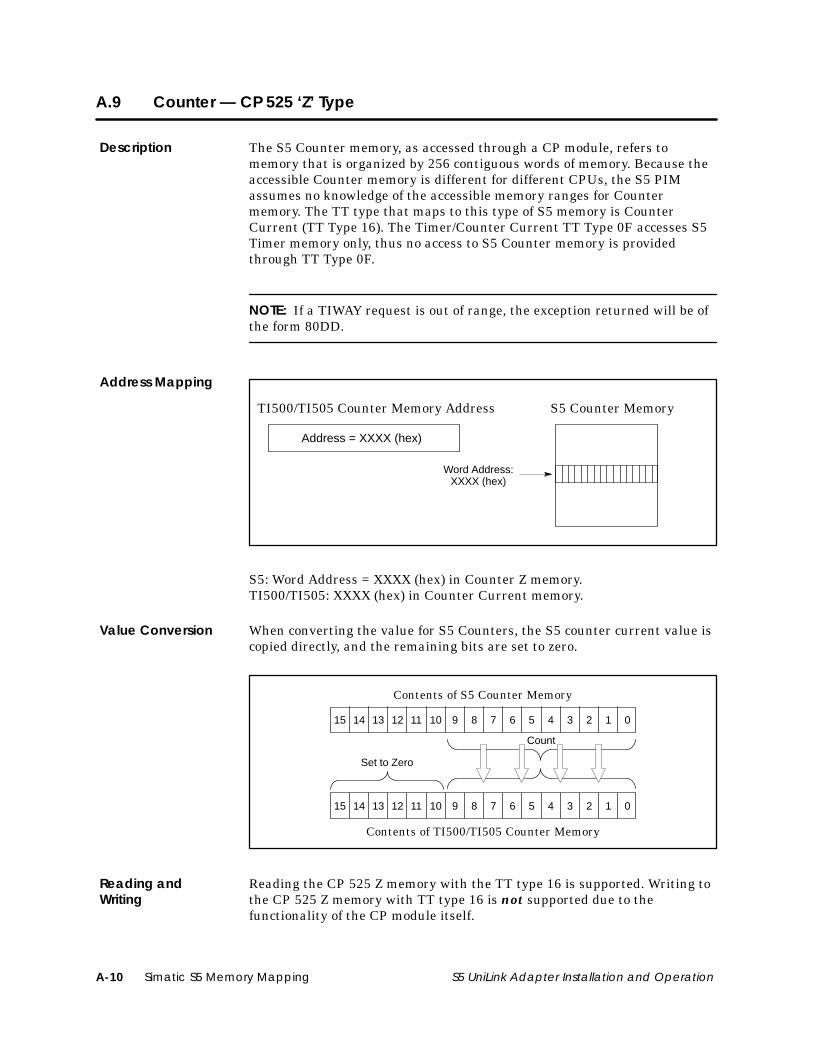
Simatic S5 Memory MappingA-10 S5 UniLink Adapter Installation and Operation
A.9 Counter — CP 525 ‘Z’ Type
The S5 Counter memory, as accessed through a CP module, refers tomemory that is organized by 256 contiguous words of memory. Because theaccessible Counter memory is different for different CPUs, the S5 PIMassumes no knowledge of the accessible memory ranges for Countermemory. The TT type that maps to this type of S5 memory is CounterCurrent (TT Type 16). The Timer/Counter Current TT Type 0F accesses S5Timer memory only, thus no access to S5 Counter memory is providedthrough TT Type 0F.
NOTE: If a TIWAY request is out of range, the exception returned will be ofthe form 80DD.
S5 Counter MemoryTI500/TI505 Counter Memory Address
Address = XXXX (hex)
Word Address:XXXX (hex)
S5: Word Address = XXXX (hex) in Counter Z memory.TI500/TI505: XXXX (hex) in Counter Current memory.
When converting the value for S5 Counters, the S5 counter current value iscopied directly, and the remaining bits are set to zero.
Contents of S5 Counter Memory
Contents of TI500/TI505 Counter Memory
15 14 13 12 11 10 9 8 7 6 5 4 3 2 1 0
15 14 13 12 11 10 9 8 7 6 5 4 3 2 1 0
Count
Set to Zero
Reading the CP 525 Z memory with the TT type 16 is supported. Writing tothe CP 525 Z memory with TT type 16 is not supported due to thefunctionality of the CP module itself.
Description
Address Mapping
Value Conversion
Reading andWriting
Simatic S5 Memory Mapping A-11S5 UniLink Adapter Installation and Operation
A.10 S5 Data Types Not Supported by S5 PIM
Due to significant differences in the internal memory structure andarchitecture between the TI500/TI505 PLCs and the S5 PLCs, nocompatible memory translations to these specific S5 data types areavailable.
The S5 Analog I/O Bytes memory type as accessed through a CP module isnot supported by the S5 PIM.
Access to Analog I/O will be through Data Block memory, which implies thatall analog conversions will be taken care of in the STEP 5 program. Thiswas determined because of the significant differences in the internalmemory representation of analog I/O.
The S5 Extended Analog I/O Bytes memory type as accessed through a CPmodule is not supported by the S5 PIM.
Access to Extended Analog I/O will be through Data Block memory, whichimplies that all analog conversions will be taken care of in the STEP 5program. This was determined because of the significant differences in theinternal memory representation of analog I/O.
The S5 Absolute Address memory type as accessed through a CP module isnot supported by the S5 PIM.
The S5 System Address memory type as accessed through a CP module isnot supported by the S5 PIM.
Analog I/O Bytes:CP 525 ‘P’ Type
Extended AnalogI/O Bytes: CP 525‘Q’ Type
Absolute Address:CP 525 ‘S’ Type
System Address:CP 525 ‘B’ Type
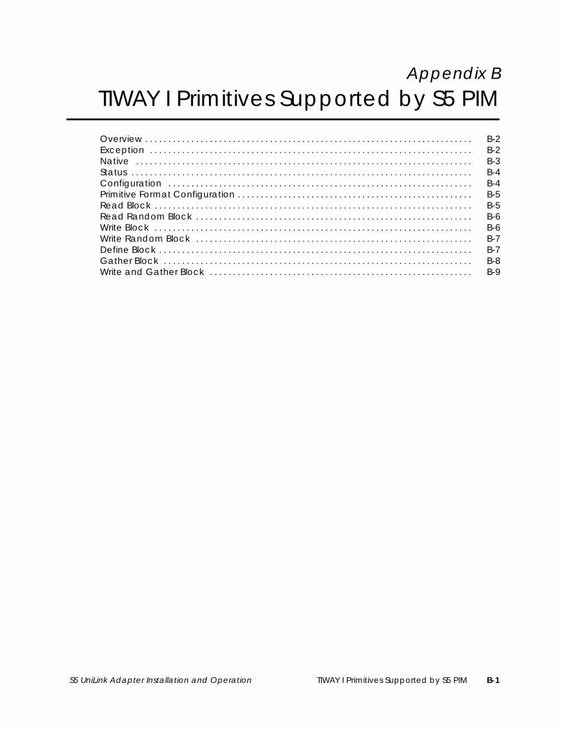
TIWAY I Primitives Supported by S5 PIM B-1S5 UniLink Adapter Installation and Operation
Appendix B
TIWAY I Primitives Supported by S5 PIM
Overview B-2. . . . . . . . . . . . . . . . . . . . . . . . . . . . . . . . . . . . . . . . . . . . . . . . . . . . . . . . . . . . . . . . . . . . . . . Exception B-2. . . . . . . . . . . . . . . . . . . . . . . . . . . . . . . . . . . . . . . . . . . . . . . . . . . . . . . . . . . . . . . . . . . . . . Native B-3. . . . . . . . . . . . . . . . . . . . . . . . . . . . . . . . . . . . . . . . . . . . . . . . . . . . . . . . . . . . . . . . . . . . . . . . . Status B-4. . . . . . . . . . . . . . . . . . . . . . . . . . . . . . . . . . . . . . . . . . . . . . . . . . . . . . . . . . . . . . . . . . . . . . . . . . Configuration B-4. . . . . . . . . . . . . . . . . . . . . . . . . . . . . . . . . . . . . . . . . . . . . . . . . . . . . . . . . . . . . . . . . . Primitive Format Configuration B-5. . . . . . . . . . . . . . . . . . . . . . . . . . . . . . . . . . . . . . . . . . . . . . . . . . . Read Block B-5. . . . . . . . . . . . . . . . . . . . . . . . . . . . . . . . . . . . . . . . . . . . . . . . . . . . . . . . . . . . . . . . . . . . . Read Random Block B-6. . . . . . . . . . . . . . . . . . . . . . . . . . . . . . . . . . . . . . . . . . . . . . . . . . . . . . . . . . . . Write Block B-6. . . . . . . . . . . . . . . . . . . . . . . . . . . . . . . . . . . . . . . . . . . . . . . . . . . . . . . . . . . . . . . . . . . . . Write Random Block B-7. . . . . . . . . . . . . . . . . . . . . . . . . . . . . . . . . . . . . . . . . . . . . . . . . . . . . . . . . . . . Define Block B-7. . . . . . . . . . . . . . . . . . . . . . . . . . . . . . . . . . . . . . . . . . . . . . . . . . . . . . . . . . . . . . . . . . . . Gather Block B-8. . . . . . . . . . . . . . . . . . . . . . . . . . . . . . . . . . . . . . . . . . . . . . . . . . . . . . . . . . . . . . . . . . . Write and Gather Block B-9. . . . . . . . . . . . . . . . . . . . . . . . . . . . . . . . . . . . . . . . . . . . . . . . . . . . . . . . .
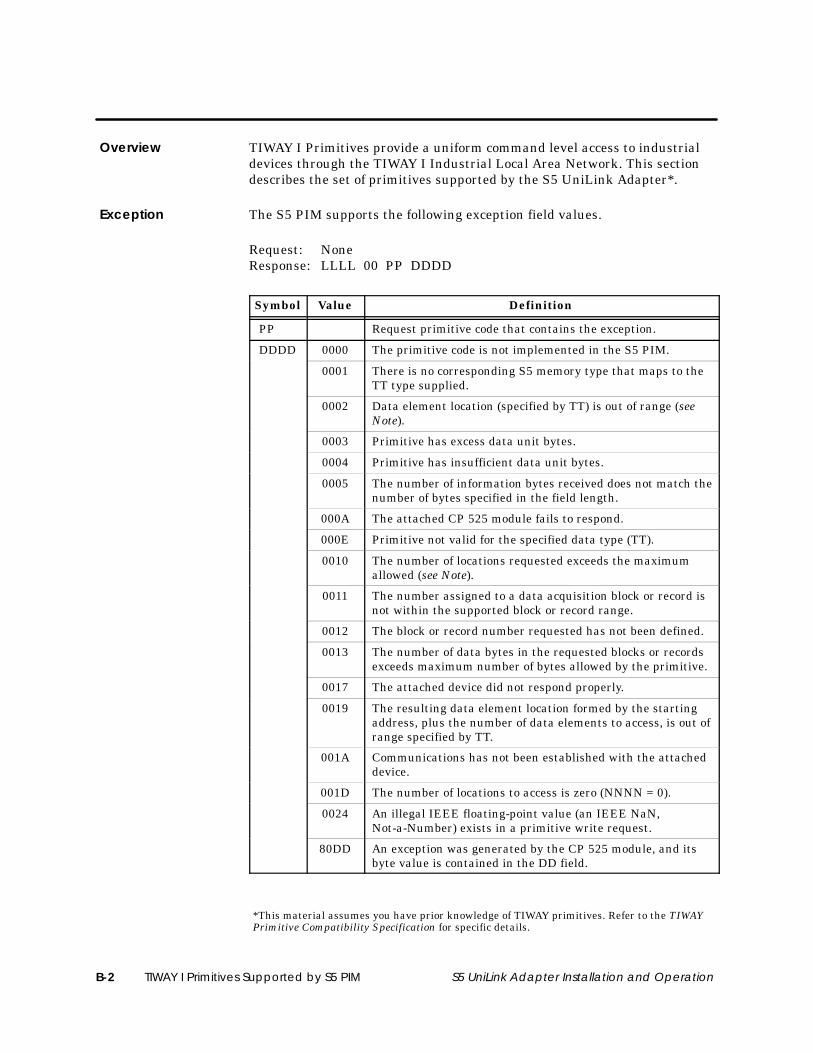
TIWAY I Primitives Supported by S5 PIMB-2 S5 UniLink Adapter Installation and Operation
TIWAY I Primitives provide a uniform command level access to industrialdevices through the TIWAY I Industrial Local Area Network. This sectiondescribes the set of primitives supported by the S5 UniLink Adapter*.
The S5 PIM supports the following exception field values.
Request: NoneResponse: LLLL 00 PP DDDD
Symbol Value Definition
PP Request primitive code that contains the exception.
DDDD 0000 The primitive code is not implemented in the S5 PIM.
0001 There is no corresponding S5 memory type that maps to theTT type supplied.
0002 Data element location (specified by TT) is out of range (seeNote).
0003 Primitive has excess data unit bytes.
0004 Primitive has insufficient data unit bytes.
0005 The number of information bytes received does not match thenumber of bytes specified in the field length.
000A The attached CP 525 module fails to respond.
000E Primitive not valid for the specified data type (TT).
0010 The number of locations requested exceeds the maximumallowed (see Note).
0011 The number assigned to a data acquisition block or record isnot within the supported block or record range.
0012 The block or record number requested has not been defined.
0013 The number of data bytes in the requested blocks or recordsexceeds maximum number of bytes allowed by the primitive.
0017 The attached device did not respond properly.
0019 The resulting data element location formed by the startingaddress, plus the number of data elements to access, is out ofrange specified by TT.
001A Communications has not been established with the attacheddevice.
001D The number of locations to access is zero (NNNN = 0).
0024 An illegal IEEE floating-point value (an IEEE NaN,Not-a-Number) exists in a primitive write request.
80DD An exception was generated by the CP 525 module, and itsbyte value is contained in the DD field.
*This material assumes you have prior knowledge of TIWAY primitives. Refer to the TIWAYPrimitive Compatibility Specification for specific details.
Overview
Exception
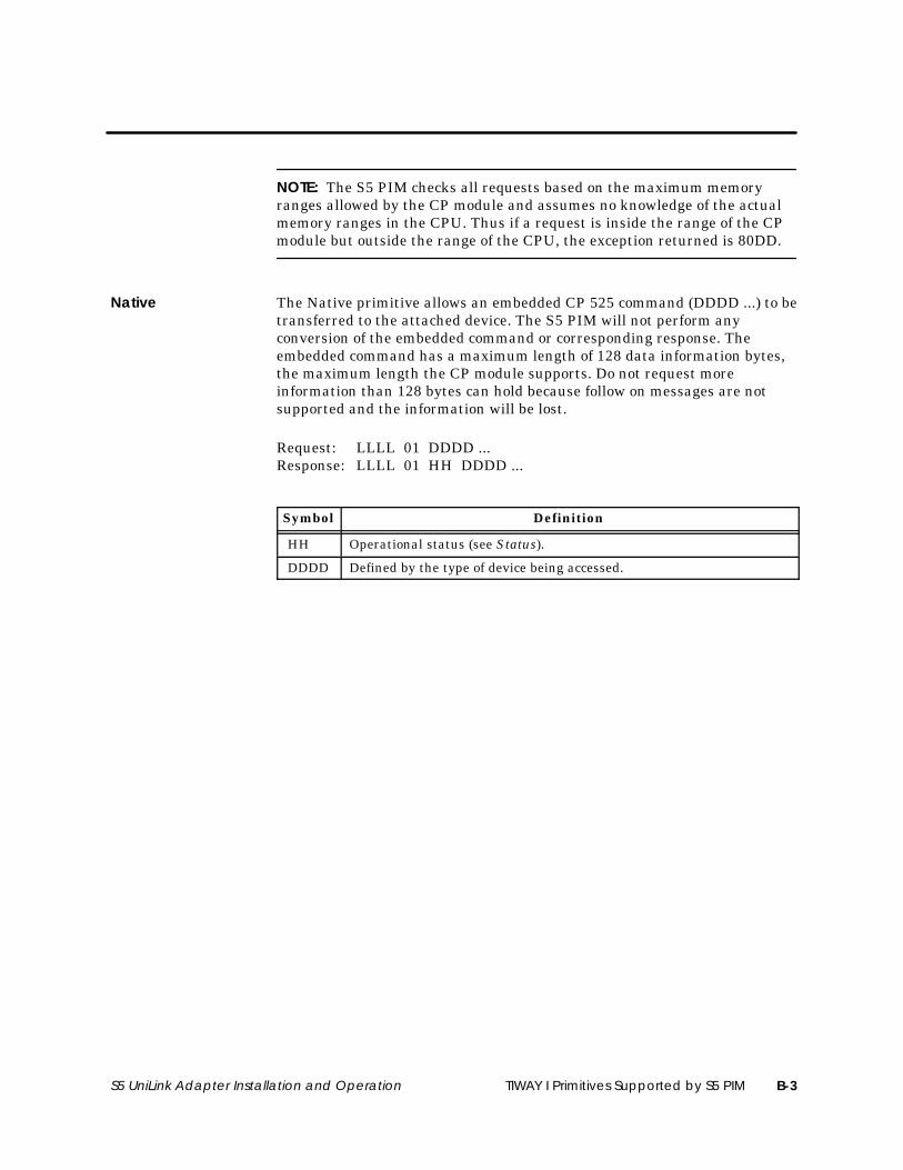
TIWAY I Primitives Supported by S5 PIM B-3S5 UniLink Adapter Installation and Operation
NOTE: The S5 PIM checks all requests based on the maximum memoryranges allowed by the CP module and assumes no knowledge of the actualmemory ranges in the CPU. Thus if a request is inside the range of the CPmodule but outside the range of the CPU, the exception returned is 80DD.
The Native primitive allows an embedded CP 525 command (DDDD ...) to betransferred to the attached device. The S5 PIM will not perform anyconversion of the embedded command or corresponding response. Theembedded command has a maximum length of 128 data information bytes,the maximum length the CP module supports. Do not request moreinformation than 128 bytes can hold because follow on messages are notsupported and the information will be lost.
Request: LLLL 01 DDDD ...Response: LLLL 01 HH DDDD ...
Symbol Definition
HH Operational status (see Status).
DDDD Defined by the type of device being accessed.
Native
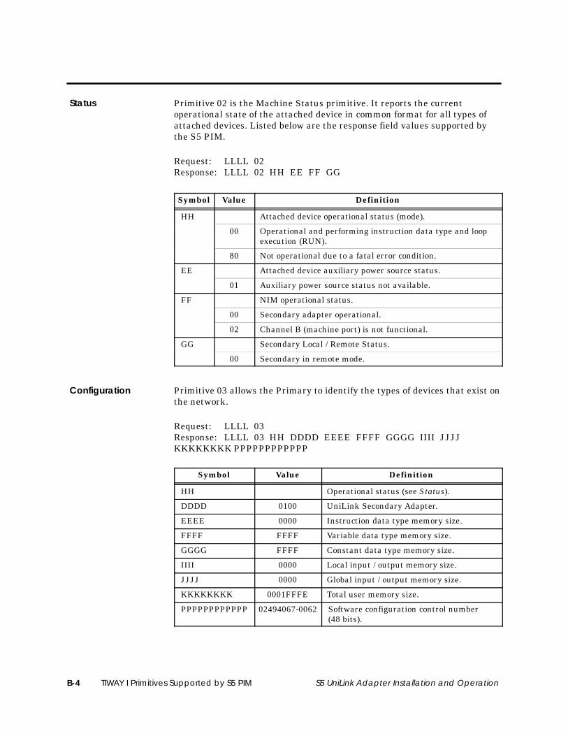
TIWAY I Primitives Supported by S5 PIMB-4 S5 UniLink Adapter Installation and Operation
Primitive 02 is the Machine Status primitive. It reports the currentoperational state of the attached device in common format for all types ofattached devices. Listed below are the response field values supported bythe S5 PIM.
Request: LLLL 02Response: LLLL 02 HH EE FF GG
Symbol Value Definition
HH Attached device operational status (mode).
00 Operational and performing instruction data type and loopexecution (RUN).
80 Not operational due to a fatal error condition.
EE Attached device auxiliary power source status.
01 Auxiliary power source status not available.
FF NIM operational status.
00 Secondary adapter operational.
02 Channel B (machine port) is not functional.
GG Secondary Local / Remote Status.
00 Secondary in remote mode.
Primitive 03 allows the Primary to identify the types of devices that exist onthe network.
Request: LLLL 03Response: LLLL 03 HH DDDD EEEE FFFF GGGG IIII JJJJKKKKKKKK PPPPPPPPPPPP
Symbol Value Definition
HH Operational status (see Status).
DDDD 0100 UniLink Secondary Adapter.
EEEE 0000 Instruction data type memory size.
FFFF FFFF Variable data type memory size.
GGGG FFFF Constant data type memory size.
IIII 0000 Local input / output memory size.
JJJJ 0000 Global input / output memory size.
KKKKKKKK 0001FFFE Total user memory size.
PPPPPPPPPPPP 02494067-0062 Software configuration control number(48 bits).
Status
Configuration
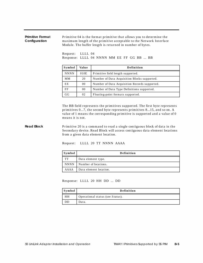
TIWAY I Primitives Supported by S5 PIM B-5S5 UniLink Adapter Installation and Operation
Primitive 04 is the format primitive that allows you to determine themaximum length of the primitive acceptable to the Network InterfaceModule. The buffer length is returned in number of bytes.
Request: LLLL 04Response: LLLL 04 NNNN MM EE FF GG BB ... BB
Symbol Value Definition
NNNN 010E Primitive field length supported.
MM 20 Number of Data Acquisition Blocks supported.
EE 00 Number of Data Acquisition Records supported.
FF 00 Number of Data Type Definitions supported.
GG 02 Floating-point formats supported.
The BB field represents the primitives supported. The first byte representsprimitives 0...7, the second byte represents primitives 8...15, and so on. Avalue of 1 means the corresponding primitive is supported and a value of 0means it is not.
Primitive 20 is a command to read a single contiguous block of data in theSecondary device. Read Block will access contiguous data element locationsfrom a given data element location.
Request: LLLL 20 TT NNNN AAAA
Symbol Definition
TT Data element type.
NNNN Number of locations.
AAAA Data element location.
Response: LLLL 20 HH DD ... DD
Symbol Definition
HH Operational status (see Status).
DD Data.
Primitive FormatConfiguration
Read Block
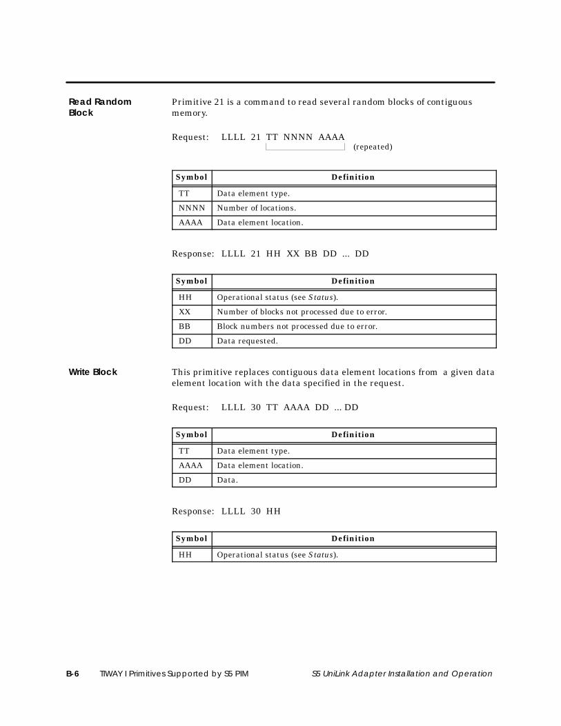
TIWAY I Primitives Supported by S5 PIMB-6 S5 UniLink Adapter Installation and Operation
Primitive 21 is a command to read several random blocks of contiguousmemory.
Request: LLLL 21 TT NNNN AAAA(repeated)
Symbol Definition
TT Data element type.
NNNN Number of locations.
AAAA Data element location.
Response: LLLL 21 HH XX BB DD ... DD
Symbol Definition
HH Operational status (see Status).
XX Number of blocks not processed due to error.
BB Block numbers not processed due to error.
DD Data requested.
This primitive replaces contiguous data element locations from a given dataelement location with the data specified in the request.
Request: LLLL 30 TT AAAA DD ... DD
Symbol Definition
TT Data element type.
AAAA Data element location.
DD Data.
Response: LLLL 30 HH
Symbol Definition
HH Operational status (see Status).
Read RandomBlock
Write Block
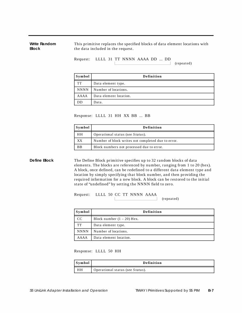
TIWAY I Primitives Supported by S5 PIM B-7S5 UniLink Adapter Installation and Operation
This primitive replaces the specified blocks of data element locations withthe data included in the request.
Request: LLLL 31 TT NNNN AAAA DD ... DD(repeated)
Symbol Definition
TT Data element type.
NNNN Number of locations.
AAAA Data element location.
DD Data.
Response: LLLL 31 HH XX BB ... BB
Symbol Definition
HH Operational status (see Status).
XX Number of block writes not completed due to error.
BB Block numbers not processed due to error.
The Define Block primitive specifies up to 32 random blocks of dataelements. The blocks are referenced by number, ranging from 1 to 20 (hex).A block, once defined, can be redefined to a different data element type andlocation by simply specifying that block number, and then providing therequired information for a new block. A block can be restored to the initialstate of “undefined” by setting the NNNN field to zero.
Request: LLLL 50 CC TT NNNN AAAA(repeated)
Symbol Definition
CC Block number (1 – 20) Hex.
TT Data element type.
NNNN Number of locations.
AAAA Data element location.
Response: LLLL 50 HH
Symbol Definition
HH Operational status (see Status).
Write RandomBlock
Define Block
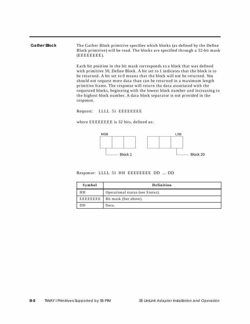
TIWAY I Primitives Supported by S5 PIMB-8 S5 UniLink Adapter Installation and Operation
The Gather Block primitive specifies which blocks (as defined by the DefineBlock primitive) will be read. The blocks are specified through a 32-bit mask(EEEEEEEE).
Each bit position in the bit mask corresponds to a block that was definedwith primitive 50, Define Block. A bit set to 1 indicates that the block is tobe returned. A bit set to 0 means that the block will not be returned. Youshould not request more data than can be returned in a maximum lengthprimitive frame. The response will return the data associated with therequested blocks, beginning with the lowest block number and increasing tothe highest block number. A data block separator is not provided in theresponse.
Request: LLLL 51 EEEEEEEE
where EEEEEEEE is 32 bits, defined as:
MSB LSB
Block 1 Block 20
Response: LLLL 51 HH EEEEEEEE DD ... DD
Symbol Definition
HH Operational status (see Status).
EEEEEEEE Bit mask (See above).
DD Data.
Gather Block
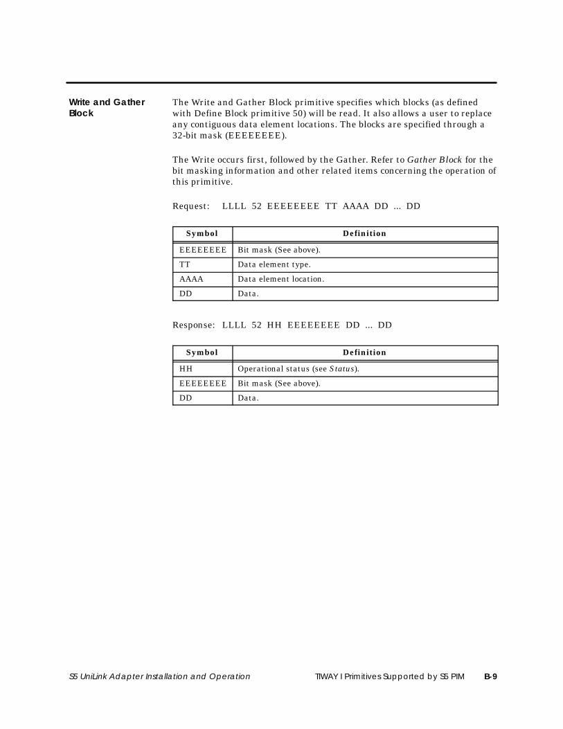
TIWAY I Primitives Supported by S5 PIM B-9S5 UniLink Adapter Installation and Operation
The Write and Gather Block primitive specifies which blocks (as definedwith Define Block primitive 50) will be read. It also allows a user to replaceany contiguous data element locations. The blocks are specified through a32-bit mask (EEEEEEEE).
The Write occurs first, followed by the Gather. Refer to Gather Block for thebit masking information and other related items concerning the operation ofthis primitive.
Request: LLLL 52 EEEEEEEE TT AAAA DD ... DD
Symbol Definition
EEEEEEEE Bit mask (See above).
TT Data element type.
AAAA Data element location.
DD Data.
Response: LLLL 52 HH EEEEEEEE DD ... DD
Symbol Definition
HH Operational status (see Status).
EEEEEEEE Bit mask (See above).
DD Data.
Write and GatherBlock
S5 Adapter/CP 525 Error Codes C-1S5 UniLink Adapter Installation and Operation
Appendix C
S5 Adapter/CP 525 Error Codes
C.1 S5 UniLink Adapter Primitive Exceptions C-2. . . . . . . . . . . . . . . . . . . . . . . . . . . . . . . . . . . . . . . . . . Primitive Exceptions C-2. . . . . . . . . . . . . . . . . . . . . . . . . . . . . . . . . . . . . . . . . . . . . . . . . . . . . . . . . . . . .
C.2 CP 525 Error Codes C-3. . . . . . . . . . . . . . . . . . . . . . . . . . . . . . . . . . . . . . . . . . . . . . . . . . . . . . . . . . . . . . Description of CP 525 Error Codes C-3. . . . . . . . . . . . . . . . . . . . . . . . . . . . . . . . . . . . . . . . . . . . . . . . Example CP 525 Error Code C-3. . . . . . . . . . . . . . . . . . . . . . . . . . . . . . . . . . . . . . . . . . . . . . . . . . . . .
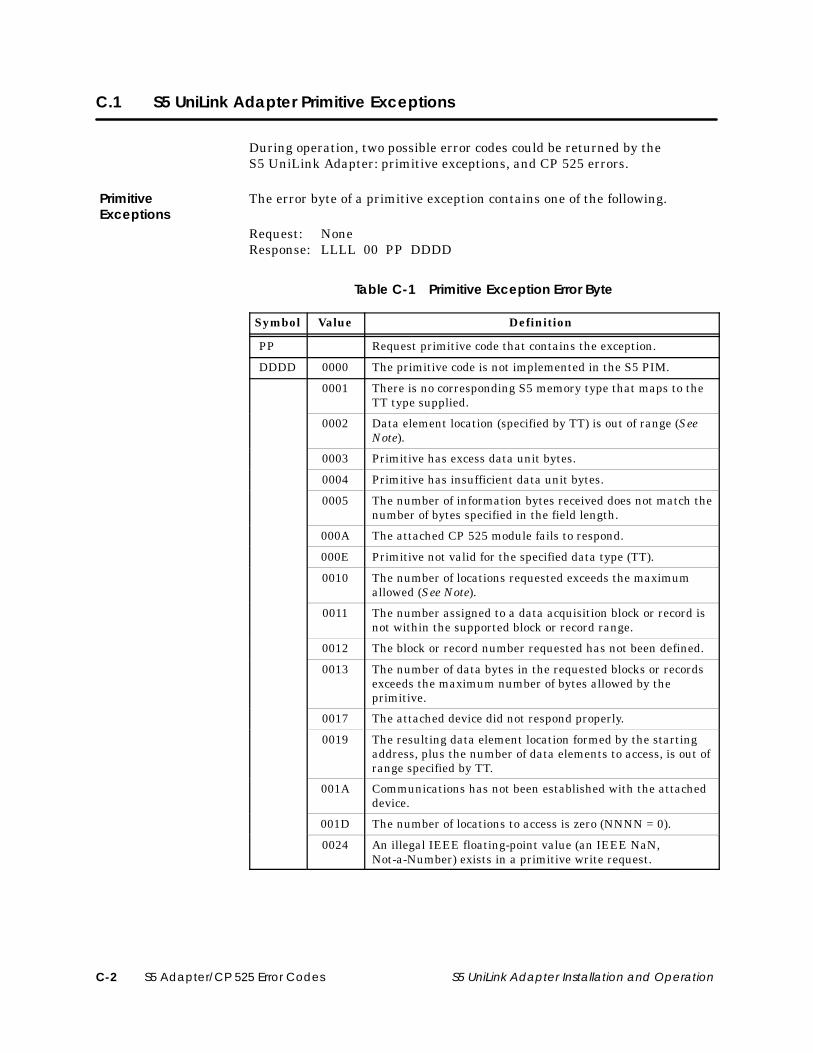
S5 Adapter/CP 525 Error CodesC-2 S5 UniLink Adapter Installation and Operation
C.1 S5 UniLink Adapter Primitive Exceptions
During operation, two possible error codes could be returned by theS5 UniLink Adapter: primitive exceptions, and CP 525 errors.
The error byte of a primitive exception contains one of the following.
Request: NoneResponse: LLLL 00 PP DDDD
Table C-1 Primitive Exception Error Byte
Symbol Value Definition
PP Request primitive code that contains the exception.
DDDD 0000 The primitive code is not implemented in the S5 PIM.
0001 There is no corresponding S5 memory type that maps to theTT type supplied.
0002 Data element location (specified by TT) is out of range (SeeNote).
0003 Primitive has excess data unit bytes.
0004 Primitive has insufficient data unit bytes.
0005 The number of information bytes received does not match thenumber of bytes specified in the field length.
000A The attached CP 525 module fails to respond.
000E Primitive not valid for the specified data type (TT).
0010 The number of locations requested exceeds the maximumallowed (See Note).
0011 The number assigned to a data acquisition block or record isnot within the supported block or record range.
0012 The block or record number requested has not been defined.
0013 The number of data bytes in the requested blocks or recordsexceeds the maximum number of bytes allowed by theprimitive.
0017 The attached device did not respond properly.
0019 The resulting data element location formed by the startingaddress, plus the number of data elements to access, is out ofrange specified by TT.
001A Communications has not been established with the attacheddevice.
001D The number of locations to access is zero (NNNN = 0).
0024 An illegal IEEE floating-point value (an IEEE NaN,Not-a-Number) exists in a primitive write request.
PrimitiveExceptions
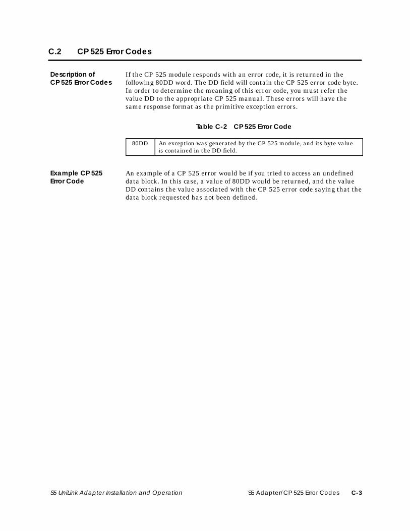
S5 Adapter/CP 525 Error Codes C-3S5 UniLink Adapter Installation and Operation
C.2 CP 525 Error Codes
If the CP 525 module responds with an error code, it is returned in thefollowing 80DD word. The DD field will contain the CP 525 error code byte.In order to determine the meaning of this error code, you must refer thevalue DD to the appropriate CP 525 manual. These errors will have thesame response format as the primitive exception errors.
Table C-2 CP 525 Error Code
80DD An exception was generated by the CP 525 module, and its byte valueis contained in the DD field.
An example of a CP 525 error would be if you tried to access an undefineddata block. In this case, a value of 80DD would be returned, and the valueDD contains the value associated with the CP 525 error code saying that thedata block requested has not been defined.
Description ofCP 525 Error Codes
Example CP 525Error Code
Index-1
Index
AAdapter
components, 1-2installing, 2-2–2-8
CCable connections
CP 525 interface port, 2-4maximum cable length, 2-5pin assignments, 2-5S5 UniLink Adapter port, 2-4
Communicationslocal line, 3-2–3-4receiving, 3964R procedure, 3-11RK 512 computer link, 3-9S5 interface, 3-9transmitting, 3964R procedure, 3-10
Computer Interface Module, 1-4
CP 525 Communications Processor, 1-2, 2-3
CP 525 memory types‘A’ type, A-7‘D’ type, A-4‘E’ type, A-6‘M’ type, A-8‘T’ type, A-9‘X’ type, A-5‘Z’ type, A-10unsupported types, A-11
‘B’ type, A-11‘P’ type, A-11‘Q’ type, A-11‘S’ type, A-11
CPU number, 2-6, 2-7
DDipswitches
dipswitch 1 settings, 2-7dipswitch 2 settings, 2-7location, 2-6purpose, 2-6
EError codes
CP 525, C-3UniLink, C-2
FFloating-point
conversion, A-3S5 value, A-3TI500/TI505 value, A-3
HHDLC protocol, 3-8
IInstallation, 2-2–2-8
Installing the PIM, 2-8
Intelligent modems, 3-6
Interfacelocal line, 3-2S5 interface port, 3-9
LLocal area network
Network Interface Modules, 1-4TIWAY I network, 1-4
Local Line interfacebus structure, 3-3data transmission parameters, 3-4pin assignments, 3-3ports, 3-2primary network, 3-2redundant media, 3-2
Index-2
MManuals, ix
Memoryquick reference chart, A-2types, A-2
Memory typesSee also CP 525 memory typesabsolute address, A-11analog I/O bytes, A-11counter, A-10data block, A-4extended analog I/O bytes, A-11extended data block, A-5flag bytes, A-8input bytes, A-6output bytes, A-7S5-supported types, 1-5system address, A-11timer, A-9
Modem interface portsconnector type, 3-5pin assignments, 3-5specifications, 3-6
NNon-intelligent modems, 3-6
PPersonality Interface Module
description, 1-2installing, 2-8slot location, 1-3
PIM. See Personality Interface Module
Pin assignmentsCP 525 connector, 2-5local line, 3-3modem (RS-232), 3-5S5 Adapter connector, 2-5
Primitive command set, 1-5
Primitive commandsconfiguration, B-4define block, B-7exception, B-2gather block, B-8native, B-3primitive format configuration, B-5read block, B-5read random block, B-6status, B-4write and gather block, B-9write block, B-6write random block, B-7
Primitive exceptions, C-2
Programmable controllers, 1-2, 1-4
Programming, CP 525 module, 2-3
ProtocolHDLC, 3-8network, 3-8RK 512, 1-2
RRedundant media
alternate channel port, 3-7transmission, 3-7
Runaway transmitter recovery, 3-6
SS5 interface
pin assignments, 2-5ports, 2-4, 2-6
S5 UniLink Adaptercomponents, 1-2description of, 1-2models, 3-2setting up, 2-2
S5-supported primitives, 1-5
S5 PLCs, 1-2
Index-3
T
Technical assistance, x
TIWAY I networkconnecting S5 PLCs, 1-4local area network, 1-4Network Interface Modules, 1-4parameters, 2-7port, 2-6
protocol, 3-8
UUniLink models, x, 3-2
VVoltage supply, x, 3-2

Customer Registration
We would like to know what you think about our user manuals so that we can serve you better.How would you rate the quality of our manuals?
Excellent Good Fair Poor
AccuracyOrganizationClarityCompletenessOverall designSizeIndex
Would you be interested in giving us more detailed comments about our manuals?
Yes! Please send me a questionnaire.
No. Thanks anyway.
Your Name:
Title:
Telephone Number: ( )
Company Name:
Company Address:
Manual Name: S5 UniLink Adapter Installation and Operation Edition: Second
Assembly No.: 2587871–0065 Date: 04/94
Order Number: PPX:TIWAY–8126–2
BUSINESS REPLY MAILFIRST CLASS PERMIT NO.3 JOHNSON CITY, TN
FOLD
FOLD
POSTAGE WILL BE PAID BY ADDRESSEE
NO POSTAGENECESSARYIF MAILED
IN THEUNITED STATES
SIEMENS INDUSTRIAL AUTOMATION, INC. 3000 BILL GARLAND RD.P.O. BOX 1255JOHNSON CITY TN 37605–1255
ATTN: Technical Communications M/S 3519

������� � �� ���� �� ������ ���
����� �� ���� ����� � ������� �� �� ���� �� ������ �� ����� ���������� �� �
������ �� � �� ���� �� !"� �� �� ��#���� ��� � �� �� �
������ ������ ���$�� � ���%� �� �� ���� �� ��&'��������� �� ��#���� �
(�� �� � ��)����� �� ���� �� ���#�� �� ������