Embed Size (px)
Citation preview
1
Design for Manufacturability with Deep Subwavelength
Lithography
David Z. PanDept. of Electrical and Computer Engineering
University of Texas at Austin
http://www.cerc.utexas.edu/utda
ICDFN, Hangzhou, 8/16/06
2
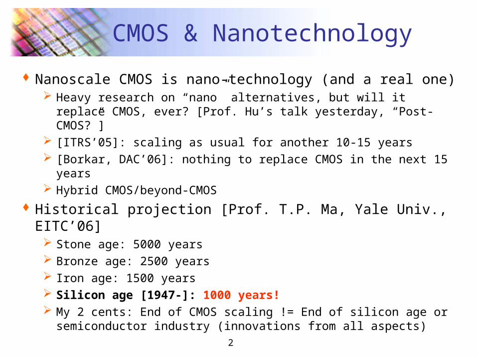
CMOS & Nanotechnology
Nanoscale CMOS is nano-technology (and a real one) Heavy research on “nano” alternatives, but will it replace CMOS,
ever? [Prof. Hu’s talk yesterday, “Post-CMOS?”] [ITRS’05]: scaling as usual for another 10-15 years [Borkar, DAC’06]: nothing to replace CMOS in the next 15 years Hybrid CMOS/beyond-CMOS
Historical projection [Prof. T.P. Ma, Yale Univ., EITC’06] Stone age: 5000 years Bronze age: 2500 years Iron age: 1500 years Silicon age [1947-]: 1000 years! My 2 cents: End of CMOS scaling != End of silicon age or
semiconductor industry (innovations from all aspects)
3
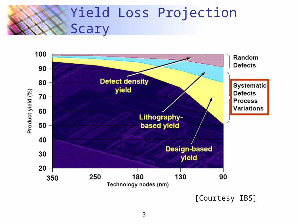
Yield Loss Projection Scary
[Courtesy IBS]
4
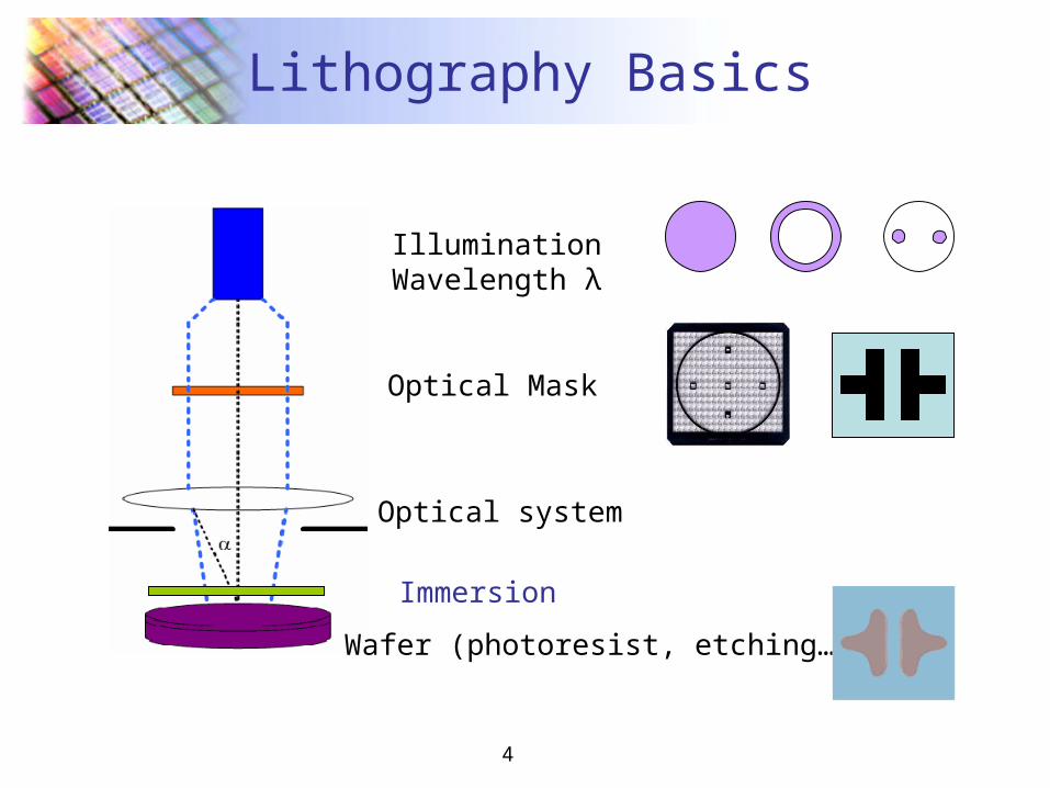
Lithography Basics
IlluminationWavelength λ
Optical Mask
Optical system
Wafer (photoresist, etching…)
Immersion
5
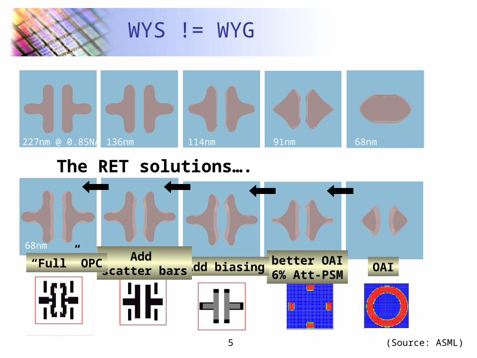
WYS != WYG
227nm @ 0.85NA 136nm 114nm 91nm 68nm
The RET solutions….
OAIbetter OAI
6% Att-PSMAdd biasing
Add scatter bars
“Full” OPC
68nm
(Source: ASML)
6
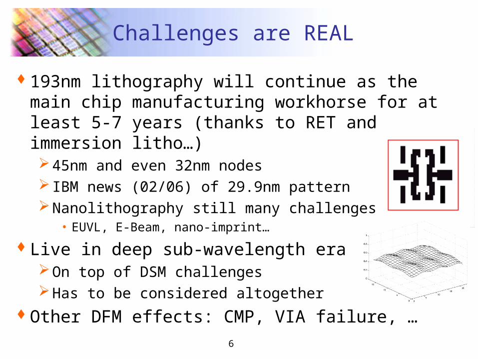
Challenges are REAL
193nm lithography will continue as the main chip manufacturing workhorse for at least 5-7 years (thanks to RET and immersion litho…)45nm and even 32nm nodes IBM news (02/06) of 29.9nm patternNanolithography still many challenges
• EUVL, E-Beam, nano-imprint…
Live in deep sub-wavelength eraOn top of DSM challengesHas to be considered altogether
Other DFM effects: CMP, VIA failure, …
7
Call for True DFM
Current “DFM” still mostly post-D(esign): data prepOften too late to fix all the problemsLittle flexibilityNot much design-intent containedNo global picture and tradeoff with other objectives
True DFM: model/predict downstream MFG/Litho effects into analysis and optimization The root cause of litho-induced layout-dependent
variations Improve yield (both functional and parametric), with less
cost, faster time to market…
8
Overall Objective/Highlights
We aim at holistic modeling, characterization, and optimization of systematic and layout-dependent variations
Bottom-up framework to tackle the heart of DFMVariational lithography modeling to predict layout-
dependent CD variations [DAC’05, DAC’06]Non-rectangular gate characterizations [ICCAD’06]Statistical/static timing/power analysis [ICCAD’06]Lithography/CMP aware physical design [DAC’05],
[DAC’06], [ICCAD’06]Variation-tolerant design [ICCAD’05], [ISPD05/06]…
9
Overall Objective/Highlights
We aim at holistic modeling, characterization, and optimization of systematic and layout-dependent variations
Bottom-up framework to tackle the heart of DFMVariational lithography modeling to predict layout-
dependent CD variations [DAC’05, DAC’06]Non-rectangular gate characterizations [ICCAD’06]Statistical/static timing/power analysis [ICCAD’06]Lithography/CMP aware physical design [DAC’05],
[DAC’06], [ICCAD’06]Variation-tolerant design [ICCAD’05], [ISPD05/06]…
10
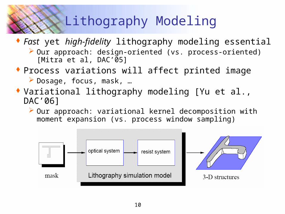
Lithography Modeling Fast yet high-fidelity lithography modeling essential
Our approach: design-oriented (vs. process-oriented) [Mitra et al, DAC’05]
Process variations will affect printed image Dosage, focus, mask, …
Variational lithography modeling [Yu et al., DAC’06] Our approach: variational kernel decomposition with moment
expansion (vs. process window sampling)
11
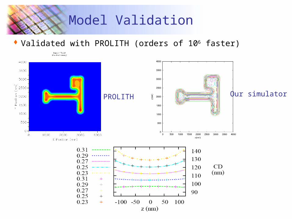
Model Validation
Validated with PROLITH (orders of 106 faster)
PROLITH Our simulator
12
RADAR: RET-Aware Detailed Routing [Mitra et al, DAC’05]
Raise lithography modeling up to design implementation levelModel-based vs. rule-based
Conventional approaches to “separate” design from manufacturing – RULES
Rules are starting running out of steam from 65nmExploding number of rulesVERY complicated rules (have you seen a Law book?)Not accurate any more…
Use our design-oriented lithography simulation to generate litho-hotspots and guide routing
13
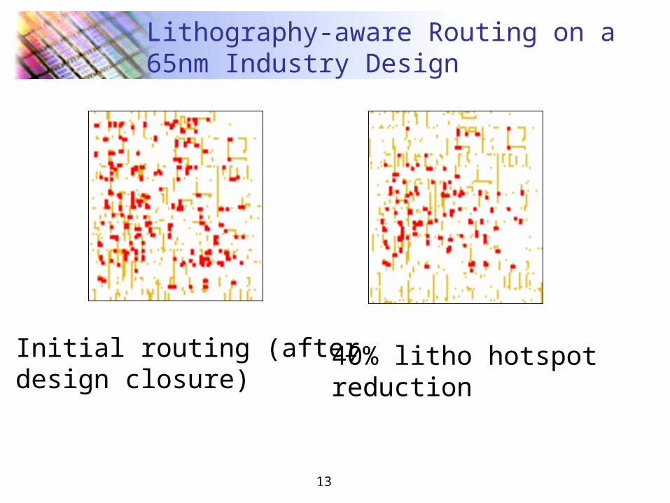
Lithography-aware Routing on a 65nm Industry Design
Initial routing (afterdesign closure)
40% litho hotspotreduction
14
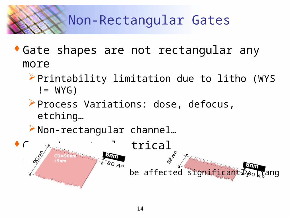
Non-Rectangular Gates
Gate shapes are not rectangular any morePrintability limitation due to litho (WYS != WYG)Process Variations: dose, defocus, etching…Non-rectangular channel…
Geometry => electrical characterization Timing/leakage may be affected significantly [Yang et al, DAC’05]
15
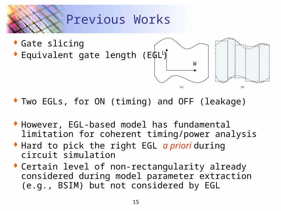
Previous Works
Gate slicing Equivalent gate length (EGL)
Two EGLs, for ON (timing) and OFF (leakage)
However, EGL-based model has fundamental limitation for coherent timing/power analysis
Hard to pick the right EGL a priori during circuit simulation Certain level of non-rectangularity already considered
during model parameter extraction (e.g., BSIM) but not considered by EGL
(a) (b)
L
W
16
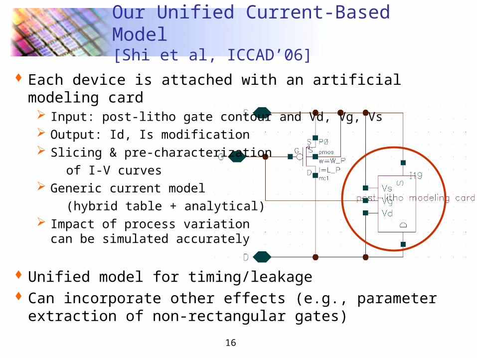
Our Unified Current-Based Model[Shi et al, ICCAD’06]
Each device is attached with an artificial modeling card Input: post-litho gate contour and Vd, Vg, Vs Output: Id, Is modification Slicing & pre-characterization
of I-V curves Generic current model
(hybrid table + analytical) Impact of process variation
can be simulated accurately
Unified model for timing/leakage Can incorporate other effects (e.g., parameter extraction of
non-rectangular gates)
17
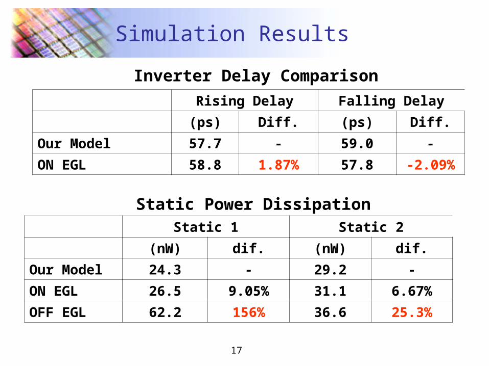
Simulation Results
Static Power DissipationStatic 1 Static 2
(nW) dif. (nW) dif.
Our Model 24.3 - 29.2 -
ON EGL 26.5 9.05% 31.1 6.67%
OFF EGL 62.2 156% 36.6 25.3%
Inverter Delay Comparison
Rising Delay Falling Delay
(ps) Diff. (ps) Diff.
Our Model 57.7 - 59.0 -
ON EGL 58.8 1.87% 57.8 -2.09%
18
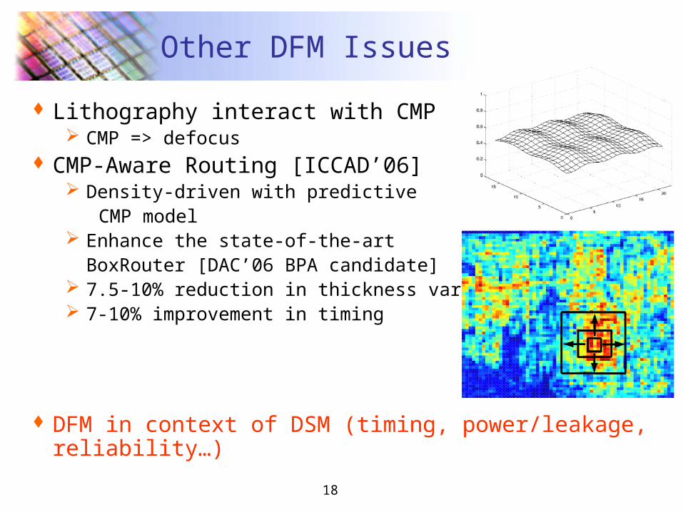
Other DFM Issues
Lithography interact with CMP CMP => defocus
CMP-Aware Routing [ICCAD’06] Density-driven with predictive CMP model Enhance the state-of-the-art
BoxRouter [DAC’06 BPA candidate] 7.5-10% reduction in thickness var. 7-10% improvement in timing
DFM in context of DSM (timing, power/leakage, reliability…)
19
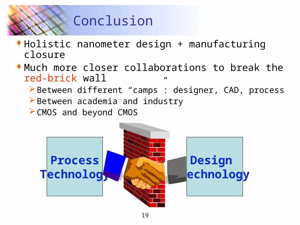
Conclusion
Holistic nanometer design + manufacturing closureMuch more closer collaborations to break the red-
brick wallBetween different “camps”: designer, CAD, processBetween academia and industryCMOS and beyond CMOS
Design Technology
ProcessTechnology
20
Silicon Age
- 1000 years to go
21
Acknowledgment
Support from SRC, IBM, Fujitsu, Sun, Intel, KLA-Tencor and Sigma-C
Graduate students at UTDA: Minsik Cho, Joydeep Mitra, Anand Ramalingam, Sean Shi, Gang Xu, Peng Yu
Collaboration/discussion with Dr. Chris Mack and Dr. Warren Grobman