Embed Size (px)
Citation preview
1806 IEEE JOURNAL OF SOLID-STATE CIRCUITS, VOL. 48, NO. 8, AUGUST 2013
Design Considerations for Interleaved ADCsBehzad Razavi, Fellow, IEEE
Abstract—Interleaving can relax the power-speed tradeoffsof analog-to-digital converters and reduce their metastabilityerror rate while increasing the input capacitance. This paperquantifies the benefits and derives an upper bound on the per-formance by considering noise and slewing requirementsof the circuit driving the system. A frequency-domain analysisof interleaved converters is also presented that sheds light onthe corruption mechanisms due to interchannel mismatches. Abackground timing mismatch calibration technique is proposedand experimentally shown to reduce the image to dB forinput frequencies exceeding 500 MHz.
Index Terms—Background calibration, flash analog-to-digitalconverters (ADCs), figure of merit, image, interleaving mis-matches, low-power ADCs, pipelined ADCs, SAR ADCs, timingmismatch.
I. INTRODUCTION
T HE concept of time interleaving was originally proposedas a means of increasing the speed of analog-to-digital
converters (ADCs) [1], albeit with a power and area penalty.However, it has since been recognized that interleaving offersadditional benefits even if absolute speed is not of primary in-terest. Such benefits accrue at the cost of other complexities,such as the need for interchannel mismatch correction [2]–[11]and multiphase clock generation.This paper presents a number of new insights into the op-
eration and performance of interleaved ADCs. Specifically,we study the power efficiency and metastability properties ofsuch ADCs and, through a frequency-domain analysis, quan-tify the effect of interchannel mismatches. We also propose abackground calibration technique for timing mismatches thatperforms detection in the digital domain and correction in theanalog domain. The reader is referred to the conference paper[12] for a survey of the prior art.Section II describes the advantages of interleaving, partic-
ularly the improvement of the figure of merit (FOM) and thereduction of metastability error rate. Section III derives anupper bound on the performance of A/D interfaces, demon-strating that the circuit driving an ADC may consume morepower than the ADC itself. Section IV analyzes the effect ofinterchannel mismatches and quantifies the effect of timingmismatch for a random input signal. Section V presents the
Manuscript received December 03, 2012; revised January 28, 2013; acceptedMarch 20, 2013. Date of publication May 13, 2013; date of current version July19, 2013. This paper was approved by Guest Editor Ken Suyama.The author is with the Electrical Engineering Department, University of Cal-
ifornia, Los Angeles, CA 90095-1594 USA (e-mail: [email protected]).Color versions of one or more of the figures in this paper are available online
at http://ieeexplore.ieee.org.Digital Object Identifier 10.1109/JSSC.2013.2258814
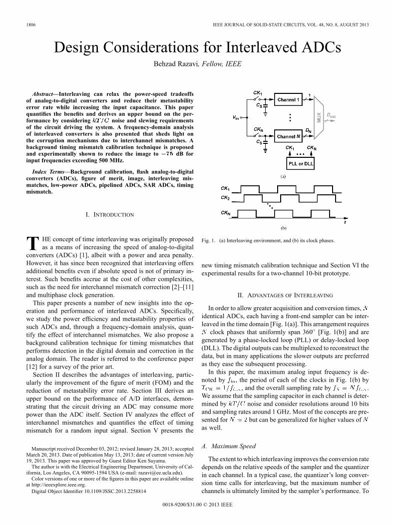
Fig. 1. (a) Interleaving environment, and (b) its clock phases.
new timing mismatch calibration technique and Section VI theexperimental results for a two-channel 10-bit prototype.
II. ADVANTAGES OF INTERLEAVING
In order to allow greater acquisition and conversion times,identical ADCs, each having a front-end sampler can be inter-leaved in the time domain [Fig. 1(a)]. This arrangement requiresclock phases that uniformly span 360 [Fig. 1(b)] and are
generated by a phase-locked loop (PLL) or delay-locked loop(DLL). The digital outputs can be multiplexed to reconstruct thedata, but in many applications the slower outputs are preferredas they ease the subsequent processing.In this paper, the maximum analog input frequency is de-
noted by , the period of each of the clocks in Fig. 1(b) by, and the overall sampling rate by .
We assume that the sampling capacitor in each channel is deter-mined by noise and consider resolutions around 10 bitsand sampling rates around 1 GHz. Most of the concepts are pre-sented for but can be generalized for higher values ofas well.
A. Maximum Speed
The extent to which interleaving improves the conversion ratedepends on the relative speeds of the sampler and the quantizerin each channel. In a typical case, the quantizer’s long conver-sion time calls for interleaving, but the maximum number ofchannels is ultimately limited by the sampler’s performance. To
0018-9200/$31.00 © 2013 IEEE
RAZAVI: DESIGN CONSIDERATIONS FOR INTERLEAVED ADCS 1807
formulate this bound, first suppose a single Nyquist-rate channelis designed for minimum acquisition time through the use ofknown techniques such as switch bootstrapping. If the ADC al-lots seconds to acquisition andrequires time constants, , for the resolution of interest,then and hence
(1)
In addition, the small-signal bandwidth of the sampler (in theacquisition mode) must exceed so as to avoid significantattenuation
(2)
For resolutions higher than a few bits, (1) guarantees (2). How-ever, as the number of interleaved channels and hence the max-imum input frequency increase, (2) eventually dominates. Forchannels, we express (1) as and equate the re-
sult to (2), obtaining
(3)
Thus, if the samplers are the speed bottleneck, then interleavingbeyond provides little improvement. In general, foran -bit system to settle to 0.5 LSB, we haveand hence
(4)
(5)
For example, a 10-bit ADC designed for maximum speed neg-ligibly benefits from interleaving if .
B. Power-Speed Tradeoffs
An important attribute of time interleaving that was evidentlynot appreciated even for two decades after Black and Hodges’paper is the flexibility that it affords in the power-speed tradeoff.The work in [13] was perhaps the first to show that the overallpower consumption of a particular design reached a minimumfor four pipelined channels. Recent work on successive-approx-imation (SAR) ADCs has extensively exploited this attributeto achieve low figures of merit [11], [14]. We define FOM asthe power consumption divided by the product of and
, where ENOB denotes the effective number ofbits at an input frequency of .Interleaving improves the FOM because, as the conver-
sion speed of a single channel approaches the limits of thetechnology, the power-speed tradeoff becomes nonlinear,demanding a disproportionately higher power for a desiredincrease in speed. For example, op amps and comparatorseventually reach diminishing returns in their speed as theirpower consumption is raised. From another perspective, eachADC architecture incurs a certain “timing overhead” that doesnot easily scale with power.
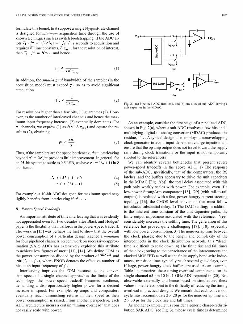
Fig. 2. (a) Pipelined ADC front end, and (b) one slice of sub-ADC driving aunit capacitor in the MDAC.
As an example, consider the first stage of a pipelined ADC,shown in Fig. 2(a), where a sub-ADC resolves a few bits and amultiplying digital-to-analog converter (MDAC) produces theresidue, . A typical design also employs a nonoverlappingclock generator to avoid input-dependent charge injection andensure that the op amp output does not travel toward the supplyrails during clock transitions or the input is not temporarilyshorted to the reference(s).We can identify several bottlenecks that present severe
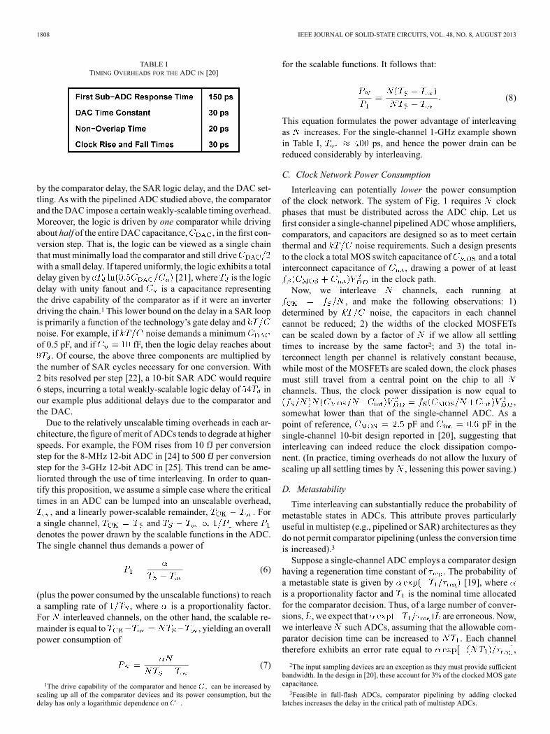
power-speed tradeoffs in the above ADC. 1) The responseof the sub-ADC, specifically, that of the comparators, the RSlatches, and the buffers necessary to drive the unit capacitorsin the MDAC [Fig. 2(b)]; the total delay associated with thispath only weakly scales with power. For example, even if alow-power StrongArm comparator [15], [29] (with rail-to-railoutputs) is replaced with a fast, power-hungry current-steeringtopology [16], the CMOS level conversion that must followintroduces substantial delay. 2) The DAC settling; in additionto the inherent time constant of the unit capacitor paths, thefinite output impedance associated with the reference, ,considerably increases the settling time. The generation of thisreference has proved quite challenging [17], [18], especiallywith low power consumption. 3) The nonoverlap time betweenthe clock phases; due to the length and complexity of theinterconnects in the clock distribution network, this “dead”time is difficult to scale down. 4) The finite rise and fall timesof the clock; owing to the capacitance of the interconnects andclocked MOSFETs as well as the finite supply bond-wire induc-tances, transition times typically reach several gate delays, evenif large, power-hungry clock buffers are used. As an example,Table I summarizes these timing overhead components for thesingle-channel 65-nm 10-bit 1-GHz ADC reported in [20]. Notobservable externally and hence based on simulations, thesevalues nonetheless point to the difficulty of reducing the timingoverhead in practical designs. We remark that each conversioncycle must accommodate 2 20 ps for the nonoverlap time and2 30 ps for the clock rise and fall times.As another example, let us consider a generic charge-redistri-
bution SAR ADC (see Fig. 3), whose cycle time is determined
1808 IEEE JOURNAL OF SOLID-STATE CIRCUITS, VOL. 48, NO. 8, AUGUST 2013
TABLE ITIMING OVERHEADS FOR THE ADC IN [20]
by the comparator delay, the SAR logic delay, and the DAC set-tling. As with the pipelined ADC studied above, the comparatorand the DAC impose a certain weakly-scalable timing overhead.Moreover, the logic is driven by one comparator while drivingabout half of the entire DAC capacitance, , in the first con-version step. That is, the logic can be viewed as a single chainthat must minimally load the comparator and still drivewith a small delay. If tapered uniformly, the logic exhibits a totaldelay given by [21], where is the logicdelay with unity fanout and is a capacitance representingthe drive capability of the comparator as if it were an inverterdriving the chain.1 This lower bound on the delay in a SAR loopis primarily a function of the technology’s gate delay andnoise. For example, if noise demands a minimumof 0.5 pF, and if fF, then the logic delay reaches about
. Of course, the above three components are multiplied bythe number of SAR cycles necessary for one conversion. With2 bits resolved per step [22], a 10-bit SAR ADC would require6 steps, incurring a total weakly-scalable logic delay of inour example plus additional delays due to the comparator andthe DAC.Due to the relatively unscalable timing overheads in each ar-
chitecture, the figure ofmerit of ADCs tends to degrade at higherspeeds. For example, the FOM rises from 10 fJ per conversionstep for the 8-MHz 12-bit ADC in [24] to 500 fJ per conversionstep for the 3-GHz 12-bit ADC in [25]. This trend can be ame-liorated through the use of time interleaving. In order to quan-tify this proposition, we assume a simple case where the criticaltimes in an ADC can be lumped into an unscalable overhead,, and a linearly power-scalable remainder, . For
a single channel, and wheredenotes the power drawn by the scalable functions in the ADC.The single channel thus demands a power of
(6)
(plus the power consumed by the unscalable functions) to reacha sampling rate of , where is a proportionality factor.For interleaved channels, on the other hand, the scalable re-mainder is equal to , yielding an overallpower consumption of
(7)
1The drive capability of the comparator and hence can be increased byscaling up all of the comparator devices and its power consumption, but thedelay has only a logarithmic dependence on .
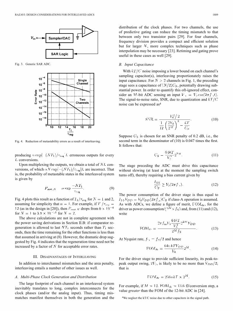
for the scalable functions. It follows that:
(8)
This equation formulates the power advantage of interleavingas increases. For the single-channel 1-GHz example shownin Table I, ps, and hence the power drain can bereduced considerably by interleaving.
C. Clock Network Power Consumption
Interleaving can potentially lower the power consumptionof the clock network. The system of Fig. 1 requires clockphases that must be distributed across the ADC chip. Let usfirst consider a single-channel pipelined ADCwhose amplifiers,comparators, and capacitors are designed so as to meet certainthermal and noise requirements. Such a design presentsto the clock a total MOS switch capacitance of and a totalinterconnect capacitance of , drawing a power of at least
in the clock path.Now, we interleave channels, each running at
, and make the following observations: 1)determined by noise, the capacitors in each channelcannot be reduced; 2) the widths of the clocked MOSFETscan be scaled down by a factor of if we allow all settlingtimes to increase by the same factor2; and 3) the total in-terconnect length per channel is relatively constant because,while most of the MOSFETs are scaled down, the clock phasesmust still travel from a central point on the chip to allchannels. Thus, the clock power dissipation is now equal to
,somewhat lower than that of the single-channel ADC. As apoint of reference, pF and pF in thesingle-channel 10-bit design reported in [20], suggesting thatinterleaving can indeed reduce the clock dissipation compo-nent. (In practice, timing overheads do not allow the luxury ofscaling up all settling times by , lessening this power saving.)
D. Metastability
Time interleaving can substantially reduce the probability ofmetastable states in ADCs. This attribute proves particularlyuseful in multistep (e.g., pipelined or SAR) architectures as theydo not permit comparator pipelining (unless the conversion timeis increased).3
Suppose a single-channel ADC employs a comparator designhaving a regeneration time constant of . The probability ofa metastable state is given by [19], whereis a proportionality factor and is the nominal time allocatedfor the comparator decision. Thus, of a large number of conver-sions, , we expect that are erroneous. Now,we interleave such ADCs, assuming that the allowable com-parator decision time can be increased to . Each channeltherefore exhibits an error rate equal to ,
2The input sampling devices are an exception as they must provide sufficientbandwidth. In the design in [20], these account for 3% of the clocked MOS gatecapacitance.3Feasible in full-flash ADCs, comparator pipelining by adding clocked
latches increases the delay in the critical path of multistep ADCs.
RAZAVI: DESIGN CONSIDERATIONS FOR INTERLEAVED ADCS 1809
Fig. 3. Generic SAR ADC.
Fig. 4. Reduction of metastability errors as a result of interleaving.
producing erroneous outputs for everyconversions.Upon multiplexing the outputs, we obtain a total of con-
versions, of which are incorrect. Thatis, the probability of metastable states in the interleaved systemis given by
(9)
Fig. 4 plots this result as a function of for and 2,assuming for simplicity that . For example, if(as in the design in [20]), then drops from
for to for .The above calculations are not in complete agreement with
the power saving derivations in Section II.B: if comparator re-generation is allowed to last seconds rather than sec-onds, then the time remaining for the other functions is less thanthat assumed in arriving at (8). However, the dramatic drop sug-gested by Fig. 4 indicates that the regeneration time need not beincreased by a factor of for acceptable error rates.
III. DISADVANTAGES OF INTERLEAVING
In addition to interchannel mismatches and the area penalty,interleaving entails a number of other issues as well.
A. Multi-Phase Clock Generation and Distribution
The large footprint of each channel in an interleaved systeminevitably translates to long, complex interconnects for theclock phases (and/or the analog input). Thus, timing mis-matches manifest themselves in both the generation and the
distribution of the clock phases. For two channels, the useof predictive gating can reduce the timing mismatch to thatbetween only two transistor pairs [29]. For four channels,frequency division provides a compact and efficient solutionbut for larger , more complex techniques such as phaseinterpolation may be necessary [23]. Retiming and gating proveuseful in these cases as well [29].
B. Input Capacitance
With noise imposing a lower bound on each channel’ssampling capacitor(s), interleaving proportionately raises theinput capacitance. For channels in Fig. 1, the precedingstage sees a capacitance of , potentially drawing sub-stantial power. In order to quantify this oft-ignored effect, con-sider an -bit ADC sensing an input .The signal-to-noise ratio, SNR, due to quantization andnoise can be expressed as4
(10)
Suppose is chosen for an SNR penalty of 0.2 dB, i.e., thesecond term in the denominator of (10) is 0.047 times the first.It follows that:
(11)
The stage preceding the ADC must drive this capacitancewithout slewing (at least at the moment the sampling switchturns off), thereby requiring a bias current given by
(12)
The power consumption of the driver stage is thus equal toif class-A operation is assumed.
As with ADCs, we define a figure of merit, , for thedriver as power consumption/ and, from (11) and (12),write
(13)
At Nyquist rate, and hence
(14)
For the driver stage to provide sufficient linearity, its peak-to-peak output swing, , is likely to be no more than ;that is
(15)
For example, if fJ/conversion step, avalue greater than the FOM of the 12-bit ADC in [24].
4We neglect the kT/C noise due to other capacitors in the signal path.
1810 IEEE JOURNAL OF SOLID-STATE CIRCUITS, VOL. 48, NO. 8, AUGUST 2013
Fig. 5. Driver FOM for different SNR penalties.
Derived from first principles, (15) places an upper bound onthe performance of A/D interfaces, indicating that the driverFOM inevitably degrades at higher resolutions. Fig. 5 plots thisFOM as a function of the resolution for different SNR penal-ties. If channels are interleaved, this FOM is multipliedby , further degrading the overall performance.5 Indepen-dent of the conversion rate, suggests that, with the rapidadvances in interleaved ADCs, the power consumption of thedriver may exceed that of the ADC itself! Note that if higherSNR penalties are allowed, then the required resolution cannotbe met. While an SNR penalty of 0.2 or 0.3 dB may appear con-servative, we point out that if the penalty is allowed to rise to,say, 3 dB, then the FOM of the ADC itself is doubled. Thus, ingeneral, the driver and the ADC must be cooptimized.
IV. EFFECT OF MISMATCHES
The effect of offset, gain and timing mismatches in an inter-leaved ADC can be analyzed in the time or frequency domainswith sinusoidal or random inputs [1]. Each of these four ap-proaches provides its own insight. We present a new frequency-domain perspective here [12] that reveals the mechanisms bywhich mismatches corrupt the analog input and exposes subtleeffects that, evidently, have not been appreciated in prior work.Let us assume that a two-channel ADC senses a random
analog input, , with a bandwidth of . The signal issampled, quantized, and multiplexed, but we ignore the effectof quantization here. If the two channels are matched, theiroutputs can be expressed as
(16)
(17)
5In architectures that allow less than for acquisition, the FOM ismultiplied by a value smaller than .
Fig. 6. Input and output spectra of a two-channel interleaved ADC.
We refer to the and samples as odd and even, respectively.In the frequency domain
(18)
(19)
Shown in Fig. 6, these spectra exhibit heavy aliasing, whichis eventually undone by the back-end multiplexer. Sincemultiplexing of discrete-time signals is equivalent to addi-tion, the spectral copies around cancel each other in
, thus yielding the original . Such cancella-tion is reminiscent of image rejection in RF receivers, pointingto the precise matching required of the channels.
A. Offset and Gain Mismatch
The effect of offset and gain mismatches has been studied ex-tensively [1], [2], [26], [30], [27]. In the absence of the inputsignal, the two ADCs digitize their own DC offsets. Conse-quently, the multiplexed output toggles between the two offsetswith a period equal to , thus exhibiting a tone at
. The power of this tone can be added to noise and har-monic powers [27] but, as an unmodulated sinusoid, it may notbe objectionable.The effect of gain mismatch can be readily observed from
the spectra in Fig. 6. As shown in Fig. 7, the spectral copiescentered at in and do not completely cancel,corrupting the baseband signal by its aliased components. Fora (voltage) gain mismatch of , we can express the power ofthese components integrated from to
as , where denotes the total power of .The signal power in is equal to because thedesired components in and add in-phase; it followsthat:
(20)
B. Timing Mismatch
The effect of timing mismatch in interleaved samplers canbe viewed as follows: if a signal, , is delayed by a smallamount, , then . Thus, the
RAZAVI: DESIGN CONSIDERATIONS FOR INTERLEAVED ADCS 1811
Fig. 7. Effect of gain mismatch in an interleaved ADC.
Fig. 8. Effect of timing mismatch with a sinusoidal input.
timing mismatch between two channels creates an error equalto .Let us first consider this effect with a sinusoidal input,
, where . As derived in [30], the multi-plexed output can be expressed as
(21)
where the second term represents an aliased component (calledthe “image” in [30]) that limits the SNR to
(22)
Fig. 8 plots the corresponding spectrum.The sinusoidal test entails two drawbacks. First, it overesti-
mates the corruption by considering only the highest input fre-quency. A realistic broadband signal would suffer maximumerror only near the edge of its bandwidth. Second, (22) does notreveal another corruption mechanism.We now analyze the effect of timing mismatch by applying
a random input signal, . For ease of illustration, we assumehas a flat spectrum from to [Fig. 9(a)]. The ad-
ditive term, , translates to in the fre-quency domain. Thus, (18) and (19) are respectively written as
(23)
(24)
Fig. 9. Effect of timing mismatch with a random input: (a) input spectrum; (b)untranslated first-order shaped component; and (c) translated first-order shapedcomponent.
We study for and . For the former case,and hence
(25)
We observe that contains itself and a new term,, which is the first-order shaped version of .
Fig. 9(b) plots the spectral density of the new term, ignoring forsimplicity the factor of predicted by (25).For , we haveand hence
(26)
The main term, , cancels a similar term in, while the shaped component aliases into the signal band
[Fig. 9(c)].It is instructive to reexamine the results obtained with a sinu-
soidal input in light of the mechanisms revealed by the randominput. The component at in Fig. 8 corresponds to thealiased term in . Butwhat in Fig. 8 corresponds to the unaliased termin ? Let us expand (21)
(27)
The first term on the right-hand side is simply a time-shiftedcopy of the second, representing the effect of sampling with atiming mismatch of . Assuming rad, we expandthe first term, obtaining
(28)
1812 IEEE JOURNAL OF SOLID-STATE CIRCUITS, VOL. 48, NO. 8, AUGUST 2013
The second term arises from the derivative of the signal, butunlike the third term, it has not experienced frequency trans-lation. Hiding behind the main component, this term has evi-dently not been considered in prior work because it is indistin-guishable from the main signal for a sinusoidal input. The equalamplitudes of the second and third terms in (28) suggest that ne-glecting the second term underestimates the corruption by 3 dB.That the derivative of a random signal corrupts the signal it-
self can be intuitively explained as follows. The correlation be-tween and can be expressed as
(29)
(30)
Interestingly, so long as is bounded, is zero, indi-cating that has no resemblance to and hence com-pletely corrupts the signal if added to it.We now wish to formulate the SNR for a finite and a
random input signal having a flat spectrum from to .Let us first find the SNR due to only the aliased spectrum ofFig. 9(c) and compare the result with (22). Integrating this spec-trum from to , we have
(31)
(32)
The desired signal power in Fig. 9(a) after multiplexing is equalto
(33)
where the factor of 4 accounts for the two copies of inand (Fig. 6). It follows that:
(34)
As expected, the SNR is higher in this case because componentslower than create less noise. The factor of 3 is reminiscent ofother situations where a “distributed” quantity is approximatedby a lumped quantity, e.g., the noise power due to the distributedgate resistance of a MOSFET [31] or the input impedance of anRC ladder [32]. In essence, (22) assumes that the signal powerdistributed from 0 to is lumped into an impulse at . (Thefactor of 3 disparity has also been recognized in [28]).In the next step, we also include the power of the unaliased
spectrum in Fig. 9(b)
(35)
This result is still 1.76 dB higher than that predicted by (22).
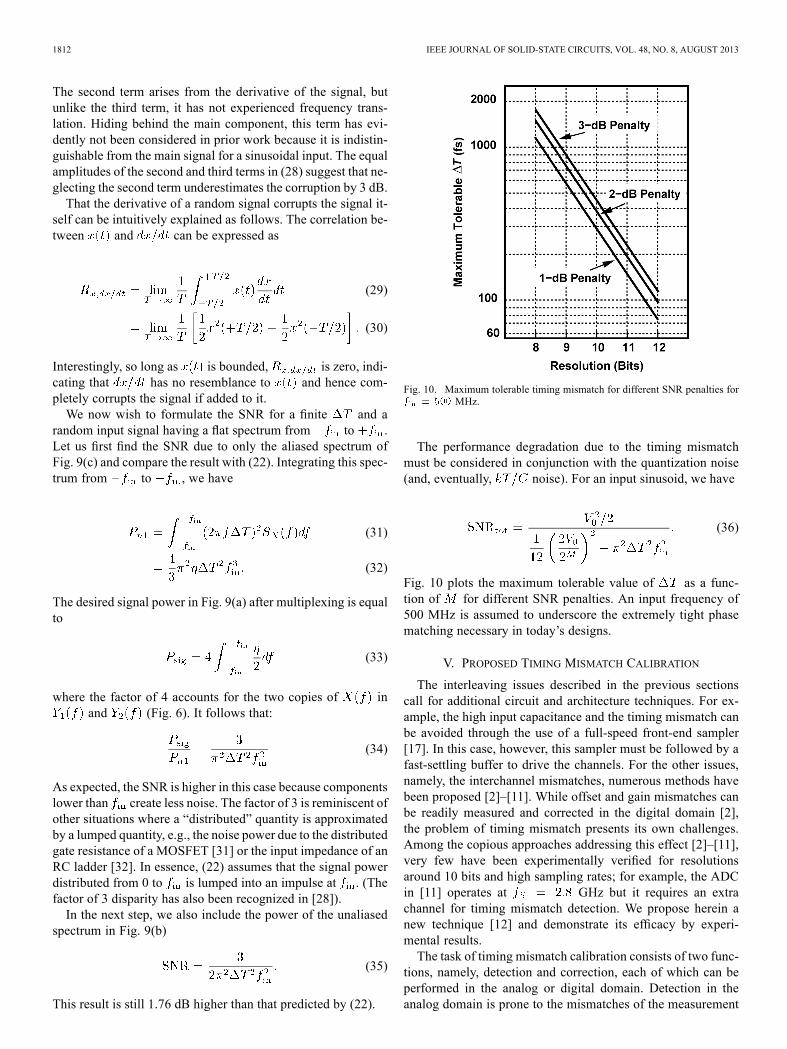
Fig. 10. Maximum tolerable timing mismatch for different SNR penalties forMHz.
The performance degradation due to the timing mismatchmust be considered in conjunction with the quantization noise(and, eventually, noise). For an input sinusoid, we have
(36)
Fig. 10 plots the maximum tolerable value of as a func-tion of for different SNR penalties. An input frequency of500 MHz is assumed to underscore the extremely tight phasematching necessary in today’s designs.
V. PROPOSED TIMING MISMATCH CALIBRATION
The interleaving issues described in the previous sectionscall for additional circuit and architecture techniques. For ex-ample, the high input capacitance and the timing mismatch canbe avoided through the use of a full-speed front-end sampler[17]. In this case, however, this sampler must be followed by afast-settling buffer to drive the channels. For the other issues,namely, the interchannel mismatches, numerous methods havebeen proposed [2]–[11]. While offset and gain mismatches canbe readily measured and corrected in the digital domain [2],the problem of timing mismatch presents its own challenges.Among the copious approaches addressing this effect [2]–[11],very few have been experimentally verified for resolutionsaround 10 bits and high sampling rates; for example, the ADCin [11] operates at GHz but it requires an extrachannel for timing mismatch detection. We propose herein anew technique [12] and demonstrate its efficacy by experi-mental results.The task of timing mismatch calibration consists of two func-
tions, namely, detection and correction, each of which can beperformed in the analog or digital domain. Detection in theanalog domain is prone to the mismatches of the measurement
RAZAVI: DESIGN CONSIDERATIONS FOR INTERLEAVED ADCS 1813
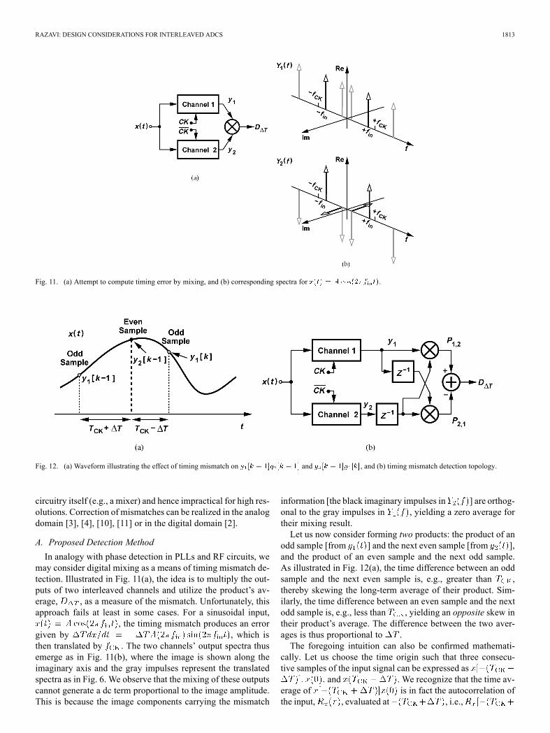
Fig. 11. (a) Attempt to compute timing error by mixing, and (b) corresponding spectra for .
Fig. 12. (a) Waveform illustrating the effect of timing mismatch on and , and (b) timing mismatch detection topology.
circuitry itself (e.g., a mixer) and hence impractical for high res-olutions. Correction of mismatches can be realized in the analogdomain [3], [4], [10], [11] or in the digital domain [2].
A. Proposed Detection Method
In analogy with phase detection in PLLs and RF circuits, wemay consider digital mixing as a means of timing mismatch de-tection. Illustrated in Fig. 11(a), the idea is to multiply the out-puts of two interleaved channels and utilize the product’s av-erage, , as a measure of the mismatch. Unfortunately, thisapproach fails at least in some cases. For a sinusoidal input,
, the timing mismatch produces an errorgiven by , which isthen translated by . The two channels’ output spectra thusemerge as in Fig. 11(b), where the image is shown along theimaginary axis and the gray impulses represent the translatedspectra as in Fig. 6. We observe that the mixing of these outputscannot generate a dc term proportional to the image amplitude.This is because the image components carrying the mismatch
information [the black imaginary impulses in ] are orthog-onal to the gray impulses in , yielding a zero average fortheir mixing result.Let us now consider forming two products: the product of an
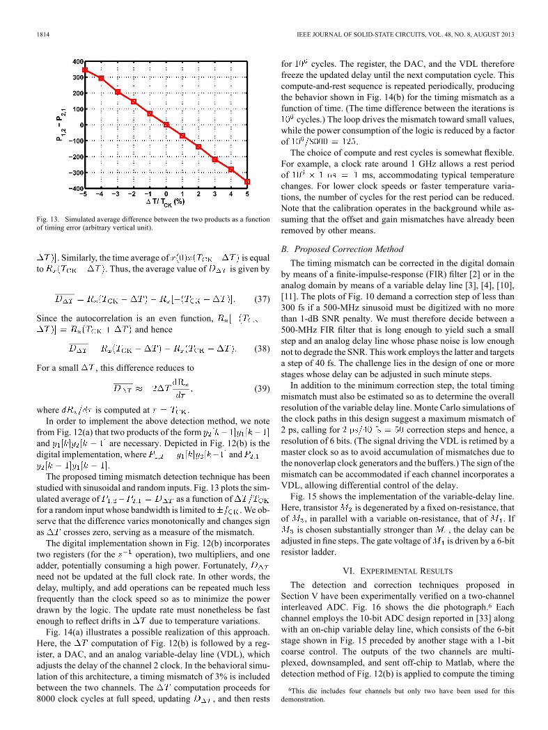
odd sample [from ] and the next even sample [from ],and the product of an even sample and the next odd sample.As illustrated in Fig. 12(a), the time difference between an oddsample and the next even sample is, e.g., greater than ,thereby skewing the long-term average of their product. Sim-ilarly, the time difference between an even sample and the nextodd sample is, e.g., less than , yielding an opposite skew intheir product’s average. The difference between the two aver-ages is thus proportional to .The foregoing intuition can also be confirmed mathemati-
cally. Let us choose the time origin such that three consecu-tive samples of the input signal can be expressed as
and . We recognize that the time av-erage of is in fact the autocorrelation ofthe input, , evaluated at , i.e.,
1814 IEEE JOURNAL OF SOLID-STATE CIRCUITS, VOL. 48, NO. 8, AUGUST 2013
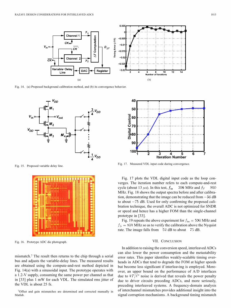
Fig. 13. Simulated average difference between the two products as a functionof timing error (arbitrary vertical unit).
. Similarly, the time average of is equalto . Thus, the average value of is given by
(37)
Since the autocorrelation is an even function,and hence
(38)
For a small , this difference reduces to
(39)
where is computed at .In order to implement the above detection method, we note
from Fig. 12(a) that two products of the formand are necessary. Depicted in Fig. 12(b) is thedigital implementation, where and
.The proposed timing mismatch detection technique has been
studied with sinusoidal and random inputs. Fig. 13 plots the sim-ulated average of as a function offor a random input whose bandwidth is limited to .We ob-serve that the difference varies monotonically and changes signas crosses zero, serving as a measure of the mismatch.The digital implementation shown in Fig. 12(b) incorporates
two registers (for the operation), two multipliers, and oneadder, potentially consuming a high power. Fortunately,need not be updated at the full clock rate. In other words, thedelay, multiply, and add operations can be repeated much lessfrequently than the clock speed so as to minimize the powerdrawn by the logic. The update rate must nonetheless be fastenough to reflect drifts in due to temperature variations.Fig. 14(a) illustrates a possible realization of this approach.
Here, the computation of Fig. 12(b) is followed by a reg-ister, a DAC, and an analog variable-delay line (VDL), whichadjusts the delay of the channel 2 clock. In the behavioral simu-lation of this architecture, a timing mismatch of 3% is includedbetween the two channels. The computation proceeds for8000 clock cycles at full speed, updating , and then rests
for cycles. The register, the DAC, and the VDL thereforefreeze the updated delay until the next computation cycle. Thiscompute-and-rest sequence is repeated periodically, producingthe behavior shown in Fig. 14(b) for the timing mismatch as afunction of time. (The time difference between the iterations is
cycles.) The loop drives the mismatch toward small values,while the power consumption of the logic is reduced by a factorof .The choice of compute and rest cycles is somewhat flexible.
For example, a clock rate around 1 GHz allows a rest periodof ms, accommodating typical temperaturechanges. For lower clock speeds or faster temperature varia-tions, the number of cycles for the rest period can be reduced.Note that the calibration operates in the background while as-suming that the offset and gain mismatches have already beenremoved by other means.
B. Proposed Correction Method
The timing mismatch can be corrected in the digital domainby means of a finite-impulse-response (FIR) filter [2] or in theanalog domain by means of a variable delay line [3], [4], [10],[11]. The plots of Fig. 10 demand a correction step of less than300 fs if a 500-MHz sinusoid must be digitized with no morethan 1-dB SNR penalty. We must therefore decide between a500-MHz FIR filter that is long enough to yield such a smallstep and an analog delay line whose phase noise is low enoughnot to degrade the SNR. This work employs the latter and targetsa step of 40 fs. The challenge lies in the design of one or morestages whose delay can be adjusted in such minute steps.In addition to the minimum correction step, the total timing
mismatch must also be estimated so as to determine the overallresolution of the variable delay line. Monte Carlo simulations ofthe clock paths in this design suggest a maximum mismatch of2 ps, calling for correction steps and hence, aresolution of 6 bits. (The signal driving the VDL is retimed by amaster clock so as to avoid accumulation of mismatches due tothe nonoverlap clock generators and the buffers.) The sign of themismatch can be accommodated if each channel incorporates aVDL, allowing differential control of the delay.Fig. 15 shows the implementation of the variable-delay line.
Here, transistor is degenerated by a fixed on-resistance, thatof , in parallel with a variable on-resistance, that of . If
is chosen substantially stronger than , the delay can beadjusted in fine steps. The gate voltage of is driven by a 6-bitresistor ladder.
VI. EXPERIMENTAL RESULTS
The detection and correction techniques proposed inSection V have been experimentally verified on a two-channelinterleaved ADC. Fig. 16 shows the die photograph.6 Eachchannel employs the 10-bit ADC design reported in [33] alongwith an on-chip variable delay line, which consists of the 6-bitstage shown in Fig. 15 preceded by another stage with a 1-bitcoarse control. The outputs of the two channels are multi-plexed, downsampled, and sent off-chip to Matlab, where thedetection method of Fig. 12(b) is applied to compute the timing
6This die includes four channels but only two have been used for thisdemonstration.
RAZAVI: DESIGN CONSIDERATIONS FOR INTERLEAVED ADCS 1815
Fig. 14. (a) Proposed background calibration method, and (b) its convergence behavior.
Fig. 15. Proposed variable delay line.
Fig. 16. Prototype ADC die photograph.
mismatch.7 The result then returns to the chip through a serialbus and adjusts the variable-delay lines. The measured resultsare obtained using the compute-and-rest method depicted inFig. 14(a) with a sinusoidal input. The prototype operates witha 1.2-V supply, consuming the same power per channel as thatin [33] plus 1 mW for each VDL. The simulated rms jitter ofthe VDL is about 25 fs.
7Offset and gain mismatches are determined and corrected manually inMatlab.
Fig. 17. Measured VDL input code during convergence.
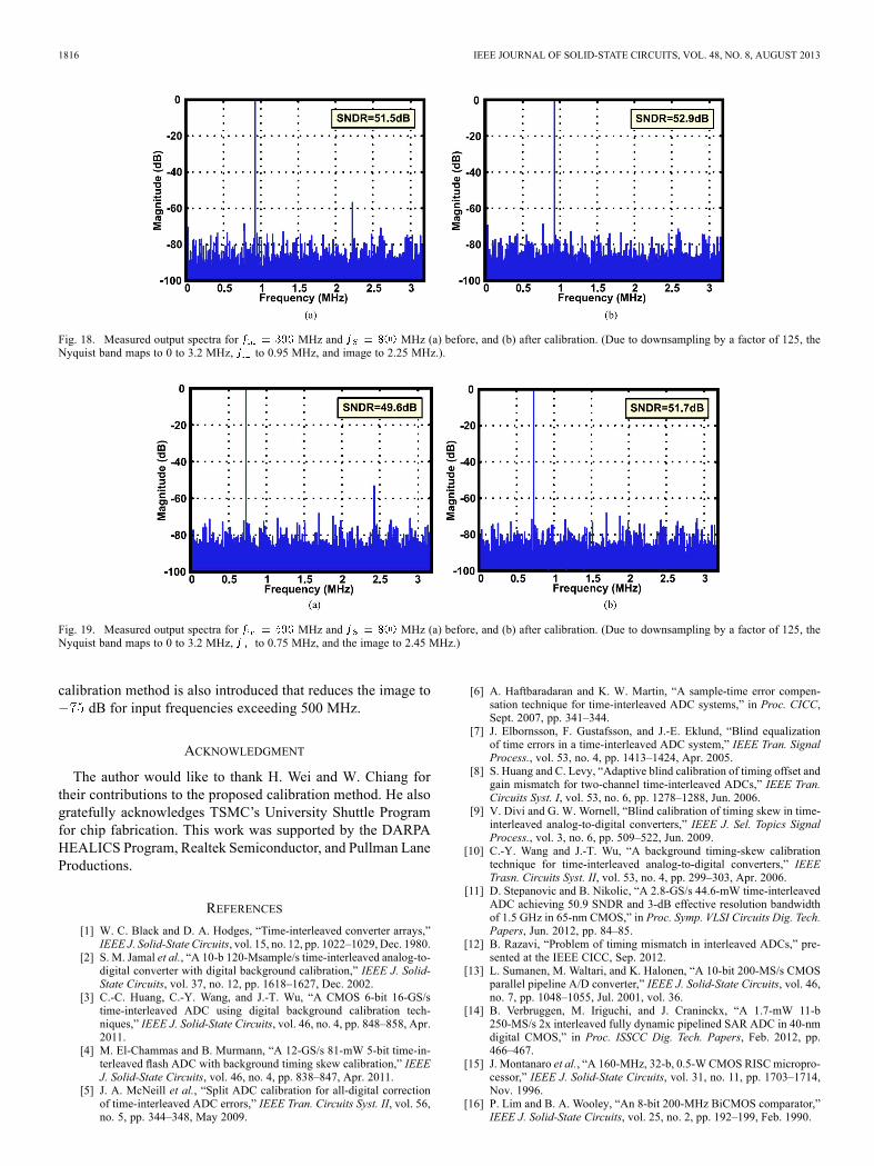
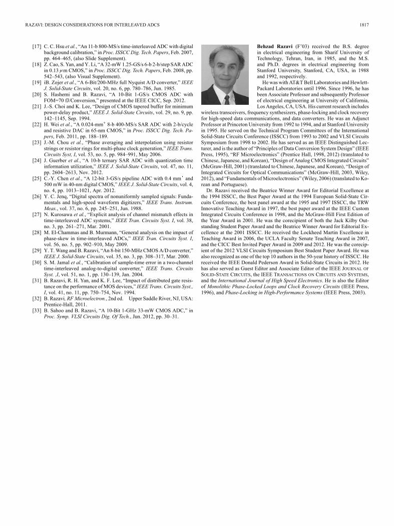
Fig. 17 plots the VDL digital input code as the loop con-verges. The iteration number refers to each compute-and-restcycle (about 13 s). In this test, MHz andMHz. Fig. 18 shows the output spectra before and after calibra-tion, demonstrating that the image can be reduced from dBto about dB. Used for only confirming the proposed cali-bration technique, the overall ADC is not optimized for SNDRor speed and hence has a higher FOM than the single-channelprototype in [33].Fig. 19 repeats the above experiment for MHz and
MHz so as to verify the calibration above the Nyquistrate. The image falls from dB to about dB.
VII. CONCLUSION
In addition to raising the conversion speed, interleaved ADCscan also lower the power consumption and the metastabilityerror rates. This paper identifies weakly-scalable timing over-heads in ADCs that tend to degrade the FOM at higher speedsbut become less significant if interleaving is employed. More-over, an upper bound on the performance of A/D interfacesdue to noise is derived that reveals the power penaltydue to driver circuits preceding ADCs, and more seriously,preceding interleaved systems. A frequency-domain analysisof interchannel mismatches provides additional insight into thesignal corruption mechanisms. A background timing mismatch
1816 IEEE JOURNAL OF SOLID-STATE CIRCUITS, VOL. 48, NO. 8, AUGUST 2013
Fig. 18. Measured output spectra for MHz and MHz (a) before, and (b) after calibration. (Due to downsampling by a factor of 125, theNyquist band maps to 0 to 3.2 MHz, to 0.95 MHz, and image to 2.25 MHz.).
Fig. 19. Measured output spectra for MHz and MHz (a) before, and (b) after calibration. (Due to downsampling by a factor of 125, theNyquist band maps to 0 to 3.2 MHz, to 0.75 MHz, and the image to 2.45 MHz.)
calibration method is also introduced that reduces the image todB for input frequencies exceeding 500 MHz.
ACKNOWLEDGMENT
The author would like to thank H. Wei and W. Chiang fortheir contributions to the proposed calibration method. He alsogratefully acknowledges TSMC’s University Shuttle Programfor chip fabrication. This work was supported by the DARPAHEALICS Program, Realtek Semiconductor, and Pullman LaneProductions.
REFERENCES
[1] W. C. Black and D. A. Hodges, “Time-interleaved converter arrays,”IEEE J. Solid-State Circuits, vol. 15, no. 12, pp. 1022–1029, Dec. 1980.
[2] S. M. Jamal et al., “A 10-b 120-Msample/s time-interleaved analog-to-digital converter with digital background calibration,” IEEE J. Solid-State Circuits, vol. 37, no. 12, pp. 1618–1627, Dec. 2002.
[3] C.-C. Huang, C.-Y. Wang, and J.-T. Wu, “A CMOS 6-bit 16-GS/stime-interleaved ADC using digital background calibration tech-niques,” IEEE J. Solid-State Circuits, vol. 46, no. 4, pp. 848–858, Apr.2011.
[4] M. El-Chammas and B. Murmann, “A 12-GS/s 81-mW 5-bit time-in-terleaved flash ADC with background timing skew calibration,” IEEEJ. Solid-State Circuits, vol. 46, no. 4, pp. 838–847, Apr. 2011.
[5] J. A. McNeill et al., “Split ADC calibration for all-digital correctionof time-interleaved ADC errors,” IEEE Tran. Circuits Syst. II, vol. 56,no. 5, pp. 344–348, May 2009.
[6] A. Haftbaradaran and K. W. Martin, “A sample-time error compen-sation technique for time-interleaved ADC systems,” in Proc. CICC,Sept. 2007, pp. 341–344.
[7] J. Elbornsson, F. Gustafsson, and J.-E. Eklund, “Blind equalizationof time errors in a time-interleaved ADC system,” IEEE Tran. SignalProcess., vol. 53, no. 4, pp. 1413–1424, Apr. 2005.
[8] S. Huang and C. Levy, “Adaptive blind calibration of timing offset andgain mismatch for two-channel time-interleaved ADCs,” IEEE Tran.Circuits Syst. I, vol. 53, no. 6, pp. 1278–1288, Jun. 2006.
[9] V. Divi and G. W. Wornell, “Blind calibration of timing skew in time-interleaved analog-to-digital converters,” IEEE J. Sel. Topics SignalProcess., vol. 3, no. 6, pp. 509–522, Jun. 2009.
[10] C.-Y. Wang and J.-T. Wu, “A background timing-skew calibrationtechnique for time-interleaved analog-to-digital converters,” IEEETrasn. Circuits Syst. II, vol. 53, no. 4, pp. 299–303, Apr. 2006.
[11] D. Stepanovic and B. Nikolic, “A 2.8-GS/s 44.6-mW time-interleavedADC achieving 50.9 SNDR and 3-dB effective resolution bandwidthof 1.5 GHz in 65-nm CMOS,” in Proc. Symp. VLSI Circuits Dig. Tech.Papers, Jun. 2012, pp. 84–85.
[12] B. Razavi, “Problem of timing mismatch in interleaved ADCs,” pre-sented at the IEEE CICC, Sep. 2012.
[13] L. Sumanen, M. Waltari, and K. Halonen, “A 10-bit 200-MS/s CMOSparallel pipeline A/D converter,” IEEE J. Solid-State Circuits, vol. 46,no. 7, pp. 1048–1055, Jul. 2001, vol. 36.
[14] B. Verbruggen, M. Iriguchi, and J. Craninckx, “A 1.7-mW 11-b250-MS/s 2x interleaved fully dynamic pipelined SAR ADC in 40-nmdigital CMOS,” in Proc. ISSCC Dig. Tech. Papers, Feb. 2012, pp.466–467.
[15] J. Montanaro et al., “A 160-MHz, 32-b, 0.5-W CMOS RISC micropro-cessor,” IEEE J. Solid-State Circuits, vol. 31, no. 11, pp. 1703–1714,Nov. 1996.
[16] P. Lim and B. A. Wooley, “An 8-bit 200-MHz BiCMOS comparator,”IEEE J. Solid-State Circuits, vol. 25, no. 2, pp. 192–199, Feb. 1990.
RAZAVI: DESIGN CONSIDERATIONS FOR INTERLEAVED ADCS 1817
[17] C. C. Hsu et al., “An 11-b 800-MS/s time-interleaved ADCwith digitalbackground calibration,” in Proc. ISSCC Dig. Tech. Papers, Feb. 2007,pp. 464–465, (also Slide Supplement).
[18] Z. Cao, S. Yan, and Y. Li, “A 32-mW1.25-GS/s 6-b 2-b/step SARADCin 0.13 m CMOS,” in Proc. ISSCC Dig. Tech. Papers, Feb. 2008, pp.542–543, (also Visual Supplement).
[19] iB. Zojer et al., “A 6-Bit/200-MHz full Nyquist A/D converter,” IEEEJ. Solid-State Circuits, vol. 20, no. 6, pp. 780–786, Jun. 1985.
[20] S. Hashemi and B. Razavi, “A 10-Bit 1-GS/s CMOS ADC withFOM=70 fJ/Conversion,” presented at the IEEE CICC, Sep. 2012.
[21] J.-S. Choi and K. Lee, “Design of CMOS tapered buffer for minimumpower-delay product,” IEEE J. Solid-State Circuits, vol. 29, no. 9, pp.142–1145, Sep. 1994.
[22] H. Wei et al., “A 0.024-mm 8-b 400-MS/s SAR ADC with 2-b/cycleand resistive DAC in 65-nm CMOS,” in Proc. ISSCC Dig. Tech. Pa-pers, Feb. 2011, pp. 188–189.
[23] J.-M. Chou et al., “Phase averaging and interpolation using resistorstrings or resistor rings for multi-phase clock generation,” IEEE Trans.Circuits Syst, I, vol. 53, no. 5, pp. 984–991, May 2006.
[24] J. Guerber et al., “A 10-b ternary SAR ADC with quantization timeinformation utilization,” IEEE J. Solid-State Circuits, vol. 47, no. 11,pp. 2604–2613, Nov. 2012.
[25] C.-Y. Chen et al., “A 12-bit 3-GS/s pipeline ADC with 0.4 mm and500 mW in 40-nm digital CMOS,” IEEE J. Solid-State Circuits, vol. 4,no. 4, pp. 1013–1021, Apr. 2012.
[26] Y. C. Jenq, “Digital spectra of nonuniformly sampled signals: Funda-mentals and high-speed waveform digitizers,” IEEE Trans. Instrum.Meas., vol. 37, no. 6, pp. 245–251, Jun. 1988.
[27] N. Kurosawa et al., “Explicit analysis of channel mismatch effects intime-interleaved ADC systems,” IEEE Tran. Circuits Syst. I, vol. 38,no. 3, pp. 261–271, Mar. 2001.
[28] M. El-Chammas and B. Murmann, “General analysis on the impact ofphase-skew in time-interleaved ADCs,” IEEE Tran. Circuits Syst. I,vol. 56, no. 5, pp. 902–910, May 2009.
[29] Y. T.Wang and B. Razavi, “An 8-bit 150-MHz CMOSA/D converter,”IEEE J. Solid-State Circuits, vol. 35, no. 3, pp. 308–317, Mar. 2000.
[30] S. M. Jamal et al., “Calibration of sample-time error in a two-channeltime-interleaved analog-to-digital converter,” IEEE Trans. CircuitsSyst. ,I, vol. 51, no. 1, pp. 130–139, Jan. 2004.
[31] B. Razavi, R. H. Yan, and K. F. Lee, “Impact of distributed gate resis-tance on the performance of MOS devices,” IEEE Trans. Circuits Syst.,I, vol. 41, no. 11, pp. 750–754, Nov. 1994.
[32] B. Razavi, RFMicroelectron., 2nd ed. Upper Saddle River, NJ, USA:Prentice-Hall, 2011.
[33] B. Sahoo and B. Razavi, “A 10-Bit 1-GHz 33-mW CMOS ADC,” inProc. Symp. VLSI Circuits Dig. Of Tech., Jun. 2012, pp. 30–31.
Behzad Razavi (F’03) received the B.S. degreein electrical engineering from Sharif University ofTechnology, Tehran, Iran, in 1985, and the M.S.and Ph.D. degrees in electrical engineering fromStanford University, Stanford, CA, USA, in 1988and 1992, respectively.Hewas with AT&TBell Laboratories and Hewlett-
Packard Laboratories until 1996. Since 1996, he hasbeen Associate Professor and subsequently Professorof electrical engineering at University of California,Los Angeles, CA, USA.His current research includes
wireless transceivers, frequency synthesizers, phase-locking and clock recoveryfor high-speed data communications, and data converters. He was an AdjunctProfessor at Princeton University from 1992 to 1994, and at Stanford Universityin 1995. He served on the Technical Program Committees of the InternationalSolid-State Circuits Conference (ISSCC) from 1993 to 2002 and VLSI CircuitsSymposium from 1998 to 2002. He has served as an IEEE Distinguished Lec-turer, and is the author of “Principles of Data Conversion SystemDesign” (IEEEPress, 1995), “RF Microelectronics” (Prentice Hall, 1998, 2012) (translated toChinese, Japanese, and Korean), “Design of Analog CMOS Integrated Circuits”(McGraw-Hill, 2001) (translated to Chinese, Japanese, and Korean), “Design ofIntegrated Circuits for Optical Communications” (McGraw-Hill, 2003, Wiley,2012), and “Fundamentals ofMicroelectronics” (Wiley, 2006) (translated to Ko-rean and Portuguese).Dr. Razavi received the Beatrice Winner Award for Editorial Excellence at
the 1994 ISSCC, the Best Paper Award at the 1994 European Solid-State Cir-cuits Conference, the best panel award at the 1995 and 1997 ISSCC, the TRWInnovative Teaching Award in 1997, the best paper award at the IEEE CustomIntegrated Circuits Conference in 1998, and the McGraw-Hill First Edition ofthe Year Award in 2001. He was the corecipient of both the Jack Kilby Out-standing Student Paper Award and the Beatrice Winner Award for Editorial Ex-cellence at the 2001 ISSCC. He received the Lockheed Martin Excellence inTeaching Award in 2006, the UCLA Faculty Senate Teaching Award in 2007,and the CICC Best Invited Paper Award in 2009 and 2012. He was the corecip-ient of the 2012 VLSI Circuits Symposium Best Student Paper Award. He wasalso recognized as one of the top 10 authors in the 50-year history of ISSCC. Hereceived the IEEE Donald Pederson Award in Solid-State Circuits in 2012. Hehas also served as Guest Editor and Associate Editor of the IEEE JOURNAL OFSOLID-STATE CIRCUITS, the IEEE TRANSACTIONS ON CIRCUITS AND SYSTEMS,and the International Journal of High Speed Electronics. He is also the Editorof Monolithic Phase-Locked Loops and Clock Recovery Circuits (IEEE Press,1996), and Phase-Locking in High-Performance Systems (IEEE Press, 2003).