Embed Size (px)
Citation preview

US 200902833.14A1
(19) United States (2) Patent Application Publication (10) Pub. No.: US 2009/0283314 A1
Ohsawa et al. (43) Pub. Date: Nov. 19, 2009
(54) WIRED CIRCUIT BOARD AND PRODUCING (30) Foreign Application Priority Data METHOD THEREOF
May 14, 2008 (JP) ................................. 2008–127234 (75) Inventors: Tetsuya Ohsawa, Osaka (JP);
Yasunari Ooyabu, Osaka (JP); Jun Publication Classification Ishii. Osaka (JP shii, Osaka (JP) (51) Int. Cl.
Correspondence Address: H05R I/II (2006.01) AKERMAN SENTERFITT H05R 3/02 (2006.01) 8100 BOONE BOULEVARD, SUITE 700 VIENNA, VA 22182-2683 (US) (52) U.S. Cl. - - - - - - - - - - - - - - - - - - - - - - - - - - - - - - - - - - - - - - - - - - - 174/261; 216/14
(73) Assignee: NITTO DENKO (57) ABSTRACT CORPORATION, Osaka (JP)
A method for producing a wired circuit board includes the (21) Appl. No.: 12/453,473 steps of integrally forming a conductive pattern, a plating lead
electrically connected with the conductive pattern, and a regulation portion provided in the plating lead to regulate penetration of an etchant into the conductive pattern; and etching the plating lead with the etchant while the regulation
(60) Provisional application No. 61/071,878, filed on May portion regulates the penetration of the etchant into the con 22, 2008. ductive pattern.
(22) Filed: May 12, 2009
Related U.S. Application Data
19
22
HUTCHINSON EXHIBIT 1003

Patent Application Publication Nov. 19, 2009 Sheet 1 of 11 US 2009/0283314 A1
HUTCHINSON EXHIBIT 1003

Patent Application Publication Nov. 19, 2009 Sheet 2 of 11 US 2009/0283314 A1
FIG. 2 (9)
( 18
§§ 13 5 T5 TT 30 12 Neº-A-DZZZZZZXZZºr'4 4. —AZZZZZZZZZZZZZZZZZZZZZZZ 3–º->>>>>>>>>>PSX-SA-X^X >>>>>.
FIG. 3
2–~~~~ 8A(6, 8) (9) 18
HUTCHINSON EXHIBIT 1003

HUTCHINSON EXHIBIT 1003
Patent Application Publication Nov. 19, 2009 Sheet 4 of 11 US 2009/0283314 A1
ls
:
HUTCHINSON EXHIBIT 1003

Patent Application Publication Nov. 19, 2009 Sheet 5 of 11 US 2009/0283314 A1
FIG. 6
FIG. 7
HUTCHINSON EXHIBIT 1003

Patent Application Publication Nov. 19, 2009 Sheet 6 of 11 US 2009/0283314 A1
FIG. 8 4.
,---? 8A(6, 8) 9(1O) 5
12
FIG. 9 8A(4, 6, 8) 5
HUTCHINSON EXHIBIT 1003

Patent Application Publication Nov. 19, 2009 Sheet 7 of 11 US 2009/0283314 A1
FIG. 1 O 18(9)
1.
FIG. 1 1 18(9)
a F-tº-ºn 5 11 2O 3O 8A 1o
* * * * * * .e.” *
HUTCHINSON EXHIBIT 1003

Patent Application Publication Nov. 19, 2009 Sheet 8 of 11 US 2009/0283314 A1
FIG. 12 18(9)
2-—º-> 8A 15 ?? 25 # so
12
HUTCHINSON EXHIBIT 1003

Patent Application Publication Nov. 19, 2009 Sheet 9 of 11 US 2009/0283314 A1
FIG. 14.
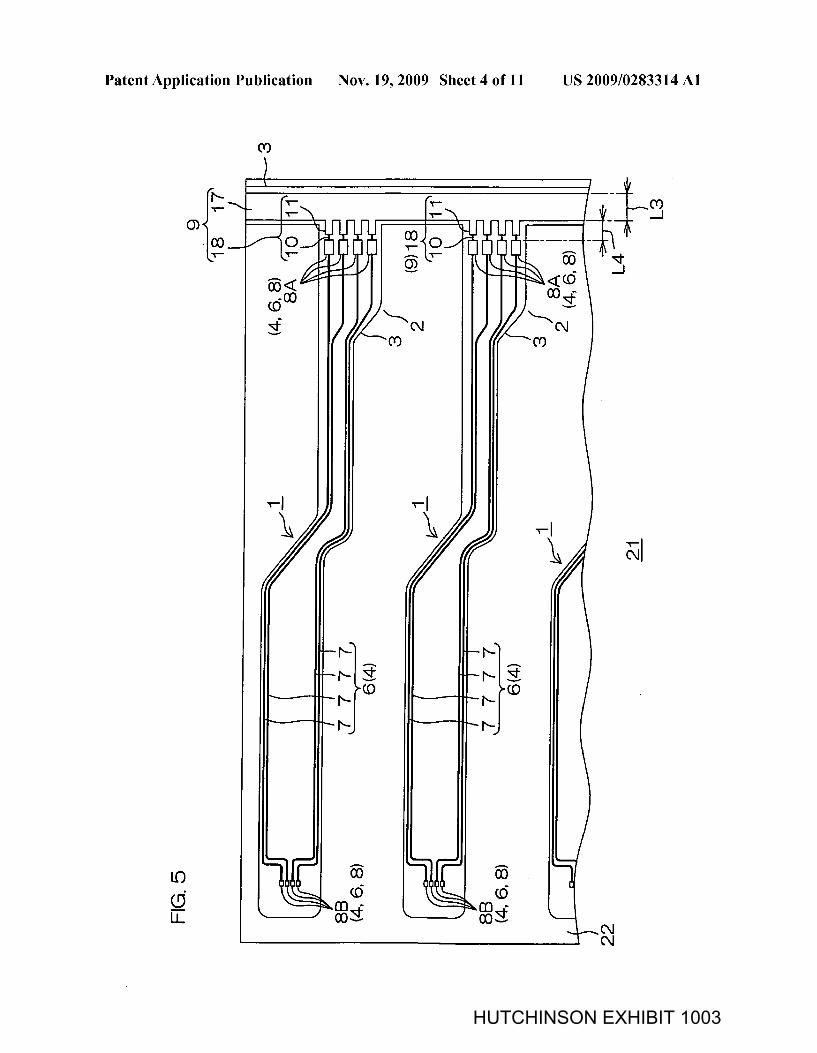
18(9)
8A 10 23 20 j 30
HUTCHINSON EXHIBIT 1003

Patent Application Publication Nov. 19, 2009 Sheet 10 of 11 US 2009/0283314 A1
FIG. 16 18(9)
PH--> --> 8A is 23–25; so
18(9) FIG. 17
/T-S--> 8A ?o 2s 255 so
- * - r - - - - - - - - - -
12
HUTCHINSON EXHIBIT 1003

Patent Application Publication Nov. 19, 2009 Sheet 11 of 11 US 2009/0283314 A1
FIG. 18
HUTCHINSON EXHIBIT 1003
US 2009/0283314 A1
WIRED CIRCUIT BOARD AND PRODUCING METHOD THEREOF
CROSS-REFERENCE TO RELATED APPLICATIONS
[0001] This patent application claims the benefit of U.S. Provisional Application No. 61/071,878, filed on May 22, 2008, and claims priority from Japanese Patent Application No. 2008-127234, filed on May 14, 2008, the contents of which are herein incorporated by reference in their entirety.
BACKGROUND OF THE INVENTION
[0002] 1. Field of the Invention [0003] The present invention relates to a wired circuitboard and a producing method thereof. More particularly, the present invention relates to a wired circuit board such as a suspension board with circuit, and a production method thereof. [0004] 2. Description of Related Art [0005] In conventional production methods of wired circuit boards such as a suspension board with circuit, a gold plating layer is provided on a surface of a terminal portion of a conductive pattern. The gold plating layer is formed by elec trolytic gold plating in which electric power is fed from feeding pads to the conductive pattern through plating leads. [0006] For example, there has been proposed a method for producing a magnetic head suspension including the follow ing steps: A conductive layer pattern and a plating lead por tion (a pad portion) which is electrically connected thereto are integrally formed on a substrate and an insulating layer, and then a covering layer for covering a part of the plating lead portion and having an opening for exposing the conductive layer pattern is formed. Subsequently, electrode pads made of gold are formed on the conductive layer pattern in the opening by feeding electric power from the plating lead portion, and then after the electrode pads are covered with a resist film, the plating lead portion exposed from the covering layer is removed by etching (cf. Japanese Unexamined Patent Publi cation No. 2002-20898).
SUMMARY OF THE INVENTION
[0007] However, in the method for producing the magnetic head suspension described in Japanese Unexamined Patent Publication No. 2002-20898 mentioned above, when the plat ing lead portion is etched, the plating lead portion covered with the covering layer may be excessively etched. [0008] That is, the etchant dissolves the plating lead portion covered with the covering layer toward the conductive layer pattern side and further reaches the conductive layer pattern under the electrode pads, thereby disadvantageously causing contamination, discoloration, or dissolution of the conductive layer pattern. [0009] It is an object of the present invention to provide a wired circuit board capable of preventing a conductive pattern from being contaminated even though a plating lead is removed by etching, and a production method thereof. [0010] The method for producing a wired circuit board according to the present invention includes the steps of inte grally forming a conductive pattern, a plating lead electrically connected with the conductive pattern, and a regulation por tion provided in the plating lead to regulate penetration of an etchant into the conductive pattern; and etching the plating
Nov. 19, 2009
lead with the etchant while the regulation portion regulates the penetration of the etchant into the conductive pattern. [0011] According to this method, the conductive pattern and the plating lead provided with a regulation portion are integrally formed. Subsequently, the plating lead is etched with the etchant while the regulation portion regulates pen etration of the etchant into the conductive pattern. [0012] Therefore, after electrolytic plating by feeding elec tric power to the conductive pattern through the plating lead, the regulation portion can prevent dissolution and discolora tion caused by the etchant in the conductive pattern. [0013] The wired circuit board of the present invention includes a conductive pattern; and a plating lead electrically connected with the conductive pattern, in which the plating lead includes a regulation portion for regulating penetration of an etchant into the conductive pattern. [0014] With this wired circuit board, when the plating lead is etched after electrolytic plating by feeding electric powerto the conductive pattern through the plating lead, the regulation portion can regulate penetration of the etchant into the con ductive pattern. [0015] Therefore, the regulation portion can prevent disso lution and discoloration caused by the etchant in the conduc tive pattern. [0016] In the wired circuit board of the present invention, it is preferable that the plating lead has a narrow portion having a short length in a widthwise direction orthogonal to an oppo site direction to the conductive pattern, and a wide portion having a length in the widthwise length longer than the nar row portion, wherein at least the wide portion serves as the regulation portion. [0017] In the wired circuit board, the etchant spreads along the widthwise direction over the regulation portion that includes at least wide portion, so that it is possible to delay the penetration of the etchant in the opposite direction. [0018] Moreover, the etchant spreading along the width direction contacts a large contact area of the regulation por tion that includes at least wide portion, and the contact surface is dissolved by the etchant. Therefore, the etchant that has dissolved the contact surface has lower etching ability, so that the etchant is less likely to penetrate in the opposite direction. As a result, the regulation portion can effectively prevent penetration of the etchant in the opposite direction. [0019. In addition, residual etchantin contact with the wide portion can be easily removed by washing, so that possible contamination by the etchant can be avoided. [0020] In the wired circuit board of the present invention, it is preferable that the plating lead has a bending portion formed so as to bend in a direction of crossing the opposite direction to the conductive pattern, wherein at least the bend ing portion serves as the regulation portion. [0021] In this wired circuit board, since the regulation por tion that includes at least the bending portion bends in a cross direction, the length of the regulation portion is inevitably longer than the straight line length of the regulation portion in the opposite direction. Therefore, even if an etchant pen etrates into the regulation portion, the regulation portion can regulate the penetration of the etchant in the opposite direc tion. As a result, dissolution and discoloration caused by the etchant in the conductive pattern can be prevented effectively. [0022] The wired circuit board of the present invention includes a conductive pattern; and a covering portion for covering a regulation portion for regulating penetration of an etchant into the conductive pattern.
HUTCHINSON EXHIBIT 1003

HUTCHINSON EXHIBIT 1003

US 2009/0283314 A1
[0055] FIG. 19 shows an enlarged plan view of the second plating lead of the wired circuit board in Comparative Example 1.
DETAILED DESCRIPTION OF PREFERRED EMBODIMENTS
First Embodiment
[0056] FIG. 1 shows a plan view of a wired circuit board assembly sheet provided with a plurality offirst embodiments of a wired circuit board according to the present invention, FIG. 2 shows a sectional view of the same taken along the line A-A of FIG. 1, FIG. 3 shows an enlarged plan view of a second plating lead of the wired circuit board shown in FIG. 1, FIG. 4 is a process diagram of a production method of the wired circuit board assembly sheet shown in FIG. 1, FIG. 5 shows a plan view of the wired circuit board assembly sheetin a production process in FIG. 4(c), FIG. 6 shows an enlarged plan view of the plating lead of the wired circuit board assem bly sheet in a production process in FIG. 4(c), and FIG. 7 shows an enlarged plan view of the plating lead of the wired circuit board assembly sheet in a production process in FIG. 4(d). [0057] To clearly illustrate a relative position of a conduc tive layer 4, an insulating cover layer 5 and a plating layer 12 are omitted in FIG. 1. [0058] In FIG. 1, a wired circuit board assembly sheet (hereinafter simply abbreviated as “sheet”) 21 includes a plurality of wired circuit boards 1 such as a suspension board with circuit, each of the wired circuit boards 1 is arranged in an aligned state at spaced intervals to each other in a metal supporting board 22 having a generally rectangular sheet shape. [0059] The wired circuit board 1 is formed in a generally rectangular flat band shape extending in a lengthwise direc tion (hereinafter referred to as front-to-end direction in some cases). As shown in FIG. 2, the wired circuit board 1 includes a metal supporting layer 2, an insulating base layer 3 formed on the metal supporting layer 2, a conductive layer 4 formed on the insulating base layer 3, and an insulating cover layer 5 formed on the insulating base layer 3 so as to cover the conductive layer 4. [0060] The metal supporting layer 2 is formed from the metal supporting board 22. As a metallic material for forming the metal supporting board 22, for example, stainless steel or 42 alloy is used, or stainless steel is preferably used. [0061] As shown in FIG. 1, the lengthwise other end (here inafter referred to as rear end) portion of the metal supporting layer 2 has support openings 19 which sandwich magnetic side terminals 8B to be described later in the lengthwise direction. [0062] The metal supporting layer 2 has a thickness in the range of, for example, 10 to 100 pum, or preferably 18 to 50 plm. [0063] As an insulating material for forming the insulating base layer 3, for example, synthetic resin such as polyimide, polyether nitrile, polyether sulfone, polyethylene terephtha late, polyethylene naphthalate, or polyvinyl chloride is used. Of these synthetic resins, polyimide is preferably used. [0064] The insulating base layer 3 is formed in a pattern corresponding to a portion where the conductive layer 4 is formed. [0065] The insulating base layer 3 has a thickness in the range of, for example, 3 to 30 pm, or preferably 5 to 15 pum.
Nov. 19, 2009
[0066] As a conductive material for forming the conductive layer 4, for example, a conductive material such as copper, nickel, gold, solder, or alloys thereof is used. Preferably, copper is used. [0067] As shown in FIG. 2, the conductive layer 4 is formed on a surface of the insulating base layer 3, and integrally includes conductive patterns 6 and second plating leads 18 in the wired circuit board 1 after production. [0068] As shown in FIG. 1, the conductive patterns 6 are arranged in spaced relation to each other in a widthwise direction (a direction orthogonal to the lengthwise direction of the wired circuit board 1), and each integrally includes a plurality of wires 7 extending along the lengthwise direction and terminal portions 8 continuous with both lengthwise end portions of each wire 7. [0069] The terminal portions 8 include external terminals 8A arranged in the lengthwise one end (hereinafter referred to as front end) portions of the wires 7, and magnetic side terminals 8B arranged in the rear end portions of the wires 7. [0070] The plurality of external terminals 8A are provided so as to be connected to the front end portions of the wires 7, respectively, and each formed as a square land. Each of the external terminals 8A is connected to a read/write board, which is not shown. [0071] The plurality of magnetic side terminals 8B are pro vided so as to be connected to the rear end portions of the wires 7, respectively, and each formed as a square land. The magnetic side terminals 8B are connected to a magnetic head, which is not shown. [0072] The plurality of second plating leads 18 are pro vided corresponding to the respective external terminals 8A. Specifically, the second plating leads 18 are arranged in spaced relation to each other in the widthwise direction, and each continuously formed on the front side of each of the external terminals 8A. Therefore, the second plating leads 18 are electrically connected with the conductive patterns 6. [0073] Each of the second plating leads 18 is formed as a remaining portion obtained by dissolving a front end surface 16A (FIG.4(f)) thereof with an etchant in the etching step (cf. FIGS. 4(f) and 4(f)) to be described later, to thereby recede rearward. That is, the front end surface 16A of the second plating lead 18 is formed as an eroded surface 16B (FIG. 4 (f)) obtained by eroding the front end surface 16A rearward from afront end surface 30 of the insulating coverlayer 5 with an etchant. [0074] As shown in FIG. 3, the second plating lead 18 integrally includes a narrow portion 10 arranged adjacent to one side in the lengthwise direction (direction opposite to the external terminal 8A) of the external terminal 8A, specifically arranged forwardly adjacent to the external terminal 8A, and a wide portion 11 arranged on the front side of the narrow portion 10. [0075] Before the etching step, the second plating lead 18 is formed from a front side portion 36 and a rear side portion 35, and after the etching step, the second plating lead 18 is formed only from the rear side portion 35 because the front side portion 36 is etched away in the etching step. [0076] As shown in FIG. 3, the narrow portion 10 is formed so as to extend in the lengthwise direction, and has a generally rectangularshape in plane view having a narrow (short) width (length in widthwise direction) W1. Specifically, the narrow portions 10 is formed so as to extend toward the front side from the widthwise center of the front end portion of each of the external terminals 8A.
HUTCHINSON EXHIBIT 1003

HUTCHINSON EXHIBIT 1003

HUTCHINSON EXHIBIT 1003

HUTCHINSON EXHIBIT 1003

HUTCHINSON EXHIBIT 1003
US 2009/0283314 A1
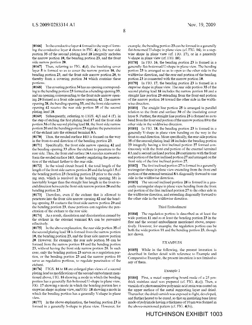
[0166] In the conductive layer 4 formed in the step of form ing the conductive layer 4 shown in FIG. 4(c), the rear side portion 35 of the second plating lead 18 integrally includes the narrow portion 10, the bending portion 23, and the front side narrow portion 20. [0167] Then, referring to FIG. 4(d), the insulating cover layer 5 is formed so as to cover the narrow portion 10, the bending portion 23, and the front side narrow portion 20, to thereby form a covering portion 34 which contains these portions. [0168] The covering portion 34 has an opening correspond ing to the bending portion 23 formed as a bending opening 33, and an opening corresponding to the front side narrow open ing 20 formed as a front side narrow opening 42. The narrow opening 28, the bending opening 33, and the frontside narrow opening 42 receive the rear side portion 35 of the second plating lead 18. [0169| Subsequently, referring to FIGS. 4(f) and 4 (f'), in the step of etching the first plating lead 17 and the front side portion 36 of the second plating lead 18, the front side narrow portion 20 and the bending portion 23 regulate the penetration of the etchant into the external terminal 8A. [0170] Thus, the eroded surface 16B is formed on the way in the front-to-end direction of the bending portion 23. [0171] Specifically, the front side narrow opening 42 and the bending opening 33 allow the etchant to penetrate to the rear side. Thus, the frontend surface 16A recedes rearward to form the eroded surface 16B, thereby regulating the penetra tion of the etchant farther to the rear side. [0172] In the wired circuit board 1, the total length of the length of the front side narrow portion 20 and the length L5 of the bending portion 23 (bending portion 23 prior to the etch ing step, which is received in the bending opening 33) is inevitably longer than the straight line length in the front-to end direction between the frontside narrow portion 20 and the bending portion 23. [0173] Therefore, even if the etchant that is allowed to penetrate into the front side narrow opening 42 and the bend ing opening 33 contacts the front side narrow portion 20 and the bending portion 23, these portions can regulate the pen etration of the etchant to the rear side. [0174] As a result, dissolution and discoloration caused by the etchant in the external terminal 8A can be prevented effectively. [0175] In the above explanation, the rear side portion 35 of the second plating lead 18 is formed from the narrow portion 10, the bending portion 23, and the front side narrow portion 20. However, for example, the rear side portion 35 can be formed from the narrow portion 10 and the bending portion 23, without having the front side narrow portion 20. In such case, only the bending portion 23 serves as a regulation por tion, or the bending portion 23 and the narrow portion 10 serve as regulation portions, to regulate penetration of the etchant. [0176] FIGS. 16 to 18 are enlarged plan views of a second plating lead as modifications of the second embodiment men tioned above, FIG. 16 showing a mode in which the bending portion has a generally flat-bottomed U-shape in plane view, FIG. 17 showing a mode in which the bending portion has a stepwise shape in plane view, and FIG. 18 showing a mode in which the bending portion has a generally V-shape in plane V1ew.
[0177] In the above explanation, the bending portion 23 is formed in a generally S-shape in plane view. However, for
Nov. 19, 2009
example, the bending portion 23 can be formed in a generally flat-bottomed U-shape in plane view (cf. FIG. 16), in a step wise shape in plane view (cf. FIG. 17), or in a generally V-shape in plane view (cf. FIG. 18). [0178] In FIG. 16, the bending portion 23 is formed in a generally flat-bottomed U-shape in plane view. The bending portion 23 is arranged so as to open to the other side in the widthwise direction, and the rear end portion of the bending portion 23 is connected with the narrow portion 10. [0179] In FIG. 17, the bending portion 23 is formed in a stepwise shape in plane view. The rear side portion 35 of the second plating lead 18 includes the narrow portion 10 and a straight line portion 25 extending from the front end portion of the narrow portion 10 toward the other side in the width wise direction. [0180] The straight line portion 25 is arranged in parallel relation to the front end surface 30 of the insulating cover layer 5. Further, the straight line portion 25 is formed so as to bend from the frontend portion of the narrow portion 10 to the other side in the widthwise direction. [0181] In FIG. 18, the bending portion 23 is formed in a generally V-shape in plane view bending on the way in the front-to-end direction. More specifically, the rear side portion 35 of the second plating lead 18 includes the bending portion 23 integrally having a first inclined portion 27 formed con tinuously with the front end portion of the external terminal 8A and a second inclined portion 28 continuous with the front end portion of the first inclined portion 27 and arranged on the front side of the first inclined portion 27. [0182] The first inclined portion 27 is formed in a generally rectangular shape in plane view extending from the front end portion of the external terminal 8A diagonally forward to one side in the widthwise direction. [0183] The second inclined portion 28 is formed in a gen erally rectangular shape in plane view bending from the front end portion of the first inclined portion 27 to the other side in the widthwise direction, and extending diagonally forward to the other side in the widthwise direction.
Third Embodiment
[0184] The regulation portion is described as at least the wide portion 11 and as at least the bending portion 23 in the first and the second embodiment mentioned above, respec tively. However, for example, the regulation portion can be both the wide portion 11 and the bending portion 23, though not shown.
EXAMPLES
[0185] While in the following, the present invention is described in further detail with reference to Example and Comparative Example, the present invention is not limited to any of them.
Example 1
[0186] First, a metal supporting board made of a 25 pum thick stainless steel was prepared (cf. FIG. 4(a)). Then, a varnish of a photosensitive polyamic acid resin was coated on the upper surface of the metal supporting layer and dried. Thereafter, the dried varnish was exposed to light, developed, and furtherheated to be cured, so that an insulating base layer made of polyimide having a thickness of 10 pum was formed in the above-mentioned pattern (cf. FIG. 4(b)).
HUTCHINSON EXHIBIT 1003

US 2009/0283314 A1
[0187| Next, a 0.03 pum-thick thin chromium film and a 0.07 pum-thick thin copper film were sequentially formed as a metal thin film on the upper surface of the insulating base layer by chromium sputtering and copper sputtering. Subse quently, a dry film resist was laminated on a surface of the metal thin film, exposed to light, and developed to form a plating resist in a pattern reverse to a conductive layer. Next, a 10 pum-thick conductive layer is formed on the surface of the metal thin film exposed from the plating resist by electrolytic copper plating. Thereafter, the plating resistand the portion of the metal thin film where the plating resist was formed were removed by etching (cf. FIG. 4(c)). [0188] The conductive layer integrally included a conduc tive pattern having wires and terminal portions, a first plating lead having a narrow portion and a wide portion in the rear side portion thereof, and a second plating lead (cf. FIGS. 5 and 6). (0189| Each of the wires had a width of 20 pum and the spacing between each of the wires was 20 pum. Each of the terminal portions had a width of 100 pum and the spacing between each of the terminal portions was 30 pm. [0190] The first plating lead had a length (L3) in the front to-end direction of 500 pum. [0191] In the second plating lead, the narrow portion had a width (W1) of 20 pum and a length (L1) in the front-to-end direction of 30 pm; and the wide portion had a width (W2) of 50 pum and a length (L2) in the front-to-end direction of 100 plm.
[0192] Next, a varnish of a photosensitive polyamic acid resin was coated on the upper surface of the insulating base layer including the conductive layer and dried. Thereafter, the dried varnish was exposed to light, developed, and further heated to be cured, so that an insulating cover layer made of polyimide having a thickness of 10 pum was formed in a pattern having a cover opening (cf. FIG. 4(d)). [0193] The insulating cover layer was provided with a cov ering portion on the front side of the external terminals, the covering portion having a narrow opening and a wide opening receiving the rear side portion of the second plating lead. The wide opening had a length (L2') in the lengthwise direction of 80 pum. [0194| Next, a plating resist was formed on surfaces of the conductive layer and the metal supporting board, except the surfaces of the terminal portions. Subsequently, a 2 plm-thick plating layer made of gold was formed on the surfaces of the respective terminal portions by electrolytic gold plating by feeding electric power to the terminal portions through the first plating lead and the second plating lead (cf. FIG. 4(e)). Thereafter, the plating resist was removed. [0195] Next, an etching resist was laminated on the sur faces of the plating layer and the metal supporting board. Subsequently, the first plating lead and the front side portion of the second plating lead were removed by etching using an aqueous ferric chloride solution (cf. FIG. 4(f)). [0196) Thereafter, the metal supporting board was washed with water and the etching resist was then removed. [0197] In the step of etching the first plating lead and the front side portion of the second plating lead, an eroded sur face which was positioned shifted rearward from the frontend surface of the insulating cover layer was formed in the wide opening (cf. FIGS. 3 and 4(f)).
Nov. 19, 2009
[0198] Thereafter, the metal supporting board was cut out to form support openings, thereby obtaining a sheet having a plurality of wired circuit boards formed thereon (cf. FIG. 1).
Comparative Example 1
[0199] The same procedures as in Example 1 were per formed except that the rear side portion (35) of the first plating lead (17) was formed only from the narrow portion (10), to thereby obtain a sheet (21) having a plurality of wired circuit boards (1) thereon (cf. FIG. 19). [0200] In the step of etching the first plating lead (17) and the front side portion (36) of the second plating lead (18), the narrow portion (10) and the front end portion of the external terminal (8A) were dissolved.
(Evaluation) 1) Presence or Absence of Discoloration of External Termi nals
[0201] In the wired circuit board on the sheet in each of Example 1 and Comparative Example 1, whether the external terminal was discolored or not was observed. [0202] The result confirmed that the external terminal in Example 1 was not discolored. [0203] On the other hand, the result confirmed that the external terminal in Comparative Example 1 was discolored. [0204] While the illustrative embodiments of the present invention are provided in the above description, such is for illustrative purpose only and it is not to be construed limita tive. Modification and variation of the present invention that will be obvious to those skilled in the art is to be covered by the following claims. What is claimed is: 1. A method for producing a wired circuit board compris
ing the steps of: integrally forming a conductive pattern, a plating lead elec
trically connected with the conductive pattern, and a regulation portion provided in the plating lead to regu late penetration of an etchant into the conductive pattern; and
etching the plating lead with the etchant while the regula tion portion regulates the penetration of the etchant into the conductive pattern.
2. A wired circuit board comprising: a conductive pattern; and a plating lead electrically connected with the conductive
pattern, wherein the plating lead comprises a regulation portion for
regulating penetration of an etchant into the conductive pattern.
3. The wired circuit board according to claim 2, wherein the plating lead has
a narrow portion having a short length in a widthwise direction orthogonal to an opposite direction to the con ductive pattern, and
a wide portion having a length in the widthwise length longer than the narrow portion,
wherein at least the wide portion serves as the regulation portion.
4. The wired circuit board according to claim 2, wherein the plating lead has a bending portion formed so as to bend
in a direction of crossing the opposite direction to the conductive pattern,
HUTCHINSON EXHIBIT 1003

US 2009/0283314 A1
wherein at least the bending portion serves as the regula tion portion.
5. A wired circuit board comprising: a conductive pattern; and a covering portion for covering a regulation portion for
regulating penetration of an etchant into the conductive pattern.
6. The wired circuit board according to claim 5, wherein a narrow opening having a short length in a widthwise
direction orthogonal to the opposite direction to the con ductive pattern and
10 Nov. 19, 2009
a wide opening having a length in the widthwise direction longer than the narrow opening are formed, in the cov ering portion,
wherein at least the wide opening receives the regulation portion.
7. The wired circuit board according to claim 5, wherein a bending opening formed so as to bend in a direction of
crossing the opposite direction to the conductive pattern is formed, in the covering portion,
wherein at least the bending opening receives the regula tion portion.
HUTCHINSON EXHIBIT 1003


![On the Ohsawa–Takegoshi L2 extension theorem and the ... · In [23], Ohsawa and Takegoshi proved the famous Ohsawa–Takegoshi L2 extension theorem, which has become an important](https://img.pdfslide.net/doc/110x75/5e3a8859deb44c560b136e5e/on-the-ohsawaatakegoshi-l2-extension-theorem-and-the-in-23-ohsawa-and-takegoshi.jpg)