Embed Size (px)
Citation preview

TSMC 2012 Corporate Social Responsibility Report
9
2. Company ProfileTSMC is the world’s largest pure-play semiconductor foundry. Founded on February 21, 1987 and headquartered in Hsinchu, Taiwan, TSMC pioneered the business model of focusing solely on manufacturing customers’ semiconductor designs. As a pure-play semiconductor foundry, the Company does not design, manufacture, or market semiconductor products under its own brand name, ensuring that TSMC does not compete directly with its customers. (TSMC Corporate Video )
With a diverse global customer base, TSMC-manufactured microchips are used in a broad variety of applications that cover various segments of the computer, communications, consumer, industrial and other electronics markets.
Annual capacity of the manufacturing facilities managed by TSMC, including subsidiaries and joint ventures, totaled 15.09 million 8-inch equivalent wafers in 2012. In Taiwan, TSMC operates three advanced 12-inch wafer fabs, four 8-inch wafer fabs, and one 6-inch wafer fab. TSMC also manages two 8-inch fabs at wholly owned subsidiaries: WaferTech in the United States and TSMC China Company Limited. In addition, TSMC obtains 8-inch wafer capacity from other companies in which the Company has an equity interest.
TSMC provides customer service through its account management and engineering services offices in North America, Europe, Japan, China, South Korea, and India. The Company employed more than 37,000 people worldwide as of the end of 2012.
TSMC 2012 Corporate Social Responsibility Report
10
TSMC continued to lead the foundry segment of the semiconductor industry in both advanced and “More-than-Moore” process technologies. Already the first foundry to provide 65nm and 40nm production capacity, TSMC in 2012 also reached full volume production of 28nm featuring 28HP & 28HPM for high performance and 28LP & 28HPL for low power, and began the initial customer tape out of 20nm technology. In addition to general-purpose logic process technology, TSMC supports the wide-ranging needs of its customers with embedded non-volatile memory, embedded DRAM, Mixed Signal/RF, high voltage, CMOS image sensor, MEMS, silicon germanium technologies and automotive service packages.
TSMC’s subsidiaries “TSMC Solid State Lighting Ltd.” and “TSMC Solar Ltd.” also respectively engage in the researching, developing, designing, manufacturing and selling of solid state lighting devices as well as related products and systems, and solar-related technologies and products.
The Company is listed on the Taiwan Stock Exchange (TWSE) under ticker number 2330, and its American Depositary Shares trade on the New York Stock Exchange (NYSE) under the symbol “TSM”.
2.1 Market/Business Summary2.1.1 TSMC AchievementsIn 2012, TSMC maintained its leading position in the total foundry segment of the global semiconductor industry, with an estimated market segment share of 45%. TSMC achieved this result amid intense competition from both established players and relatively new entrants to the business.
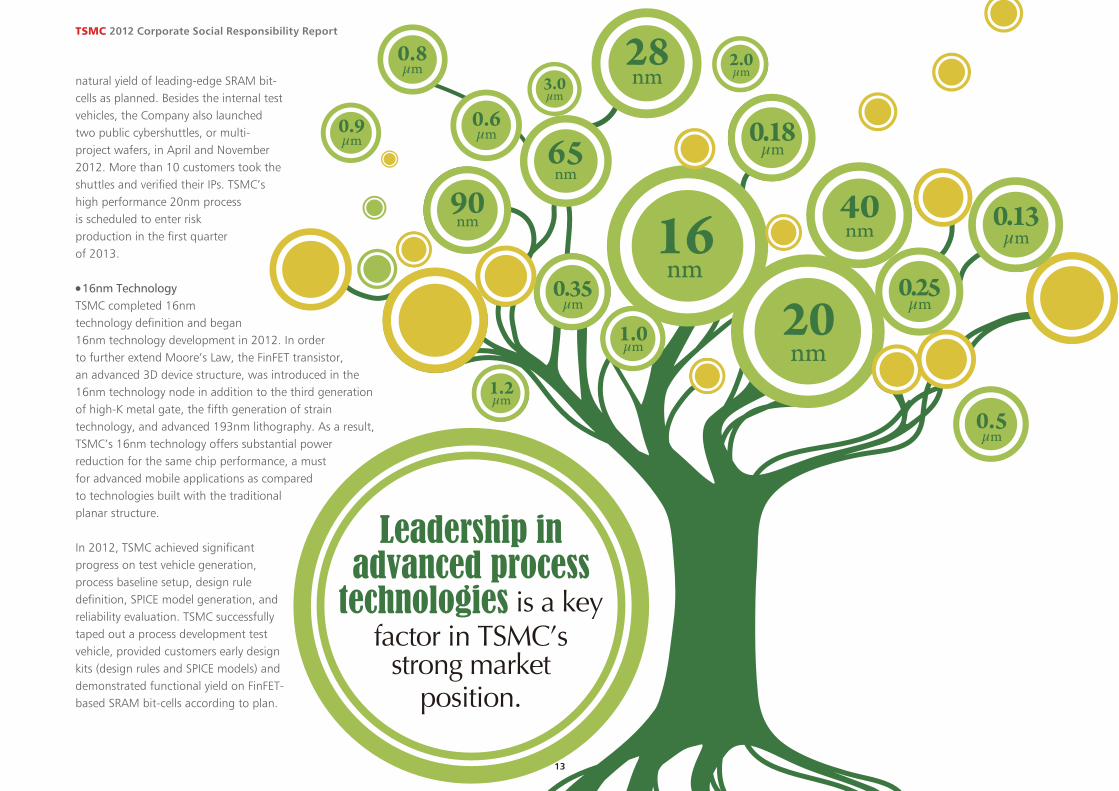
Leadership in advanced process technologies is a key factor in TSMC’s strong market position. In 2012, 77% of TSMC’s wafer revenue came from manufacturing processes with geometries of 0.13μm and below; 62% of TSMC’s wafer revenue came from 65nm processes and below.
2.1.2 Market OverviewWe estimate that the worldwide semiconductor market in 2012 reached US$308 billion in revenue, a 2% decline compared to 2011. Total foundry, a manufacturing sub-segment of the semiconductor industry, generated total revenues of US$34 billion in 2012, or 16% YoY growth.
2.1.3 Industry Outlook, Opportunities and Threats
Industry Demand and Supply OutlookFollowing 5% growth in 2011, foundry segment growth accelerated significantly by 16% in 2012, mainly driven by fabless market share gain over IDM and process technology advancement.
We forecast total semiconductor market to grow 3% YoY in 2013. Longer term, increasing semiconductor content in electronics devices, continuing market share gain of fabless, and increasing in-house ASIC from system companies, foundry sales are expected to display much stronger growth than the projected 4% compound annual growth rate (CAGR) for the total semiconductor industry from 2012 through 2017.
As an upstream supplier in the semiconductor supply chain, the condition of the foundry segment is tightly correlated with the market health of the 3Cs: communications, computer and consumer.
● CommunicationsThe communications sector, particularly the handset segment, posted a modest 5% growth in unit shipments for 2012. Smartphones, which have much higher semiconductor content, have been leading the growth of the sector.
The continuing transition to 4G/LTE handsets will bring positive momentum to the market. Smartphones with increasing performance, lower power and more intelligent features will continue to propel the buying interest of new handsets in 2013. The growing popularity of low-end smartphones in the emerging countries is also a new catalyst driving the growth of the sector.
Low power IC is an essential requirement among handset manufacturers. The System-on-Chip (SoC) design for more optimized cost, power and form-factor (i.e. device footprint), plus the appetite for higher performance to run complicated software, will continue to accelerate the migration to advanced process technologies in which TSMC is already the leader.
● ComputerThe computer sector’s unit shipment growth declined 3% YoY in 2012 after a close to flat year in 2011. Cautious spending in developed countries and budget competition from tablet products were among the factors causing the weak demand.
Moving into 2013, PC market will decline. While pessimism regarding the economic outlook will overhang the sector, new innovative features and form-factors such as detachable keyboard, hybrid notebook and the introduction of the new Windows 8 operating system are expected to stimulate PC demand.
TSMC 2012 Corporate Social Responsibility Report
11
Requirements of lower power, higher performance and integration for key computer components such as CPU, GPU, Chipset, etc., should drive product design demand for leading process technologies.
● ConsumerAfter flat sales in 2011, the consumer sector lost momentum in 2012 with a decline of 2% in aggregated unit shipment growth YoY. Economic uncertainties have stifled buyers’ appetite for consumer electronics products, and the growth of mobile computing devices has also impacted the consumer electronics sales.
Moving forward, new product launches such as the introduction of a new generation of game consoles will stimulate new interest in video games. Low-priced, large screen TVs will kindle end-consumer buying interest. And, government subsidy programs in multiple countries should drive the adoption of DTV.
Meanwhile, increasing innovations in the consumer sector have also encouraged new usage models, such as integration of touch sensing, motion recognition, high-resolution and 3D display. Besides the need for advanced technologies, “More-than-Moore” technologies such as CMOS Image Sensor (CIS), High-Voltage (HV) drivers, embedded memory, micro-controller and MEMS are becoming prominent requirements. With its comprehensive technology portfolio, TSMC will be able to capitalize on these trends.
Emerging ApplicationsEmerging new applications such as tablets are increasing contributions to foundry segment revenue. Led by Apple’s iPad, around 155 million tablets shipped in 2012 compared with 68 million units in 2011. The strong sales momentum will continue in 2013 as more models are introduced by
other OEMs. We forecast the tablet market will grow with a 23% CAGR from 2012 through 2017, and become a strong growth driver for both the semiconductor industry and foundry segment.
Supply ChainThe electronics industry consists of a long and complex supply chain, the elements of which are highly dependent and correlated with each other. At the upstream IC manufacturing level, it is important for IC vendors to have sufficient and flexible supply to support the dynamic market situation. The foundry vendors are playing an important role to ensure the health of the supply chain. As a leader in the foundry segment, TSMC provides leading technologies and large-scale capacity to complement the innovations created along the downstream chain.
2.2 Innovation ManagementInnovation is the wellspring of TSMC’s growth, and is a part of all aspects of our business, from strategic planning, marketing and management, to technology and manufacturing. At TSMC, innovation means more than new ideas, it means putting ideas into practice.
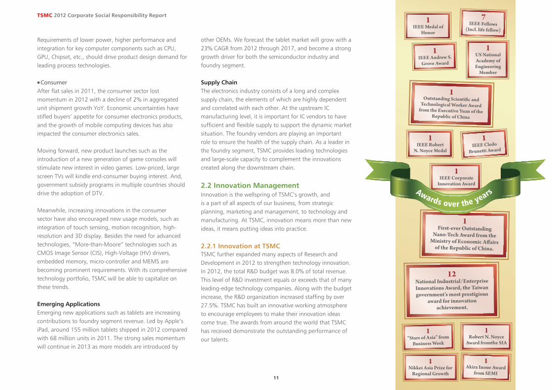
2.2.1 Innovation at TSMCTSMC further expanded many aspects of Research and Development in 2012 to strengthen technology innovation. In 2012, the total R&D budget was 8.0% of total revenue. This level of R&D investment equals or exceeds that of many leading-edge technology companies. Along with the budget increase, the R&D organization increased staffing by over 27.5%. TSMC has built an innovative working atmosphere to encourage employees to make their innovation ideas come true. The awards from around the world that TSMC has received demonstrate the outstanding performance of our talents.
TSMC 2012 Corporate Social Responsibility Report
12
2.2.2 Technology LeadershipTSMC recognizes that the technology challenge required to extend Moore’s Law, the business law behind CMOS scaling, is becoming increasingly complex. R&D Vice Presidents bring their rich industry experience to strengthen the R&D team and to navigate the technological and competitive challenges ahead. In 2012, TSMC worked intensively on ramping 28nm technology, which contributed close to 22% of fourth quarter 2012 revenue, and the contribution is expected to further increase in FY2013.
TSMC accelerated the development of advanced transistors, especially 3D transistors using FinFET structure for the 16nm process node, embedded memories, and copper (Cu)/low-K interconnect technologies. During 2012, the R&D organization once again proved its capabilities by developing 20nm technology as well as establishing 16nm transistor leadership capabilities. Furthermore, TSMC broadened the horizon of transistor research by investing R&D in alternative high-speed and low-power channel materials other than silicon, such as germanium and III-V compounds.
TSMC also expanded its external R&D partnerships and alliances with world-class research institutions. For example, TSMC is a core partner of IMEC, a respected European R&D consortium in Belgium. TSMC also has strategic agreements with IP providers to enable the development of reusable IPs for advanced technology nodes. TSMC strengthened its collaboration with key development partners on design-process optimization, and provides funding for nanotechnology research at leading research universities worldwide to promote innovations and the advancement of technology.
These research efforts enable the Company to continuously offer its customers the foundry-leading, first-to-market technologies and design solutions that contribute to their product success in today’s complex and challenging market environment.
Advance Technology InnovationsAs the semiconductor foundry leader pioneer, TSMC continued to provide technology innovations to lead the foundry segment of the semiconductor industry in both advanced and “More-than-Moore” process technologies. Not only was it the first foundry to provide 65nm and 40nm production capacity, TSMC also became the first foundry to offer volume production of 28-nanometer, with our first-to-market 28-nanometer high-k/metal gate (HKMG) technology portfolio.
● 28nm TechnologyIn 2012, TSMC’s 28nm technology offering added 28nm High Performance Plus (28HPP) and 28nm High Performance Triple-Gate (28HPT). 28HPP and 28HPT achieved 10% faster speed than that of the previous 28nm High Performance (28HP) and 28nm High Performance Mobile Computing (28HPM) processes offered in 2011. 28HPP was qualified and demonstrated first silicon success in early production. 28HPT received its first customer tape out in December 2012, and is scheduled to deliver first silicon success by April 2013.
● 20nm TechnologyIn 2012, TSMC continued to focus on 20nm technology development, including process baseline setup and yield learning, design rule definition and enhancement, SPICE model generation, and reliability evaluation. To offer a leading-edge technology for both digital and analog applications, the Company adopted an advanced lithography process for smaller feature size. With second generation of high-K metal-gate, more Si strain, and a new device structure, the intrinsic transistor performance continues to improve in line with Moore’s Law. Meanwhile, external resistance can be effectively reduced and controlled by a specially designed process technique. The back-end-of-line (BEOL) interconnect process features extreme low-K inter-metal dielectric materials and copper metallization with a novel low-resistance scheme. TSMC’s logic transistor and SRAM bit-cell offering using the 20nm process can satisfy high performance System-on-Chip (SoC) applications.
Development of 20nm technology will create superior gate density and chip performance. The cost and complexity of advanced technology will continue to escalate for customers. In 2012, TSMC successfully taped out a process development test vehicle, defect reduction vehicle, and product-like yield learning vehicle, on which an advanced ARM-core block was included. With the vehicle and process development, TSMC provided V1.0 process flow, design kits (design rules, SPICE models, and PDK files) and intellectual property (IP) in 2012 to help reduce foundry-access costs. The Company achieved its demanding transistor performance target and demonstrated the functional and
TSMC 2012 Corporate Social Responsibility Report
13
natural yield of leading-edge SRAM bit-cells as planned. Besides the internal test vehicles, the Company also launched two public cybershuttles, or multi-project wafers, in April and November 2012. More than 10 customers took the shuttles and verified their IPs. TSMC’s high performance 20nm process is scheduled to enter risk production in the first quarter of 2013.
● 16nm TechnologyTSMC completed 16nm technology definition and began 16nm technology development in 2012. In order to further extend Moore’s Law, the FinFET transistor, an advanced 3D device structure, was introduced in the 16nm technology node in addition to the third generation of high-K metal gate, the fifth generation of strain technology, and advanced 193nm lithography. As a result, TSMC’s 16nm technology offers substantial power reduction for the same chip performance, a must for advanced mobile applications as compared to technologies built with the traditional planar structure.
In 2012, TSMC achieved significant progress on test vehicle generation, process baseline setup, design rule definition, SPICE model generation, and reliability evaluation. TSMC successfully taped out a process development test vehicle, provided customers early design kits (design rules and SPICE models) and demonstrated functional yield on FinFET-based SRAM bit-cells according to plan.
TSMC 2012 Corporate Social Responsibility Report
14
● Lithography20nm lithography progressed steadily in 2012. There has been continuous learning and improvement in material quality, process recipe robustness, and litho-cell maintenance that have resulted in robust patterning solutions. The achieved defect learning and D0 goals enable successful yield learning on SRAM qualification vehicles and several key customer tape-outs.
Lithography for the 16nm node signifies the introduction of novel patterning techniques to achieve 48nm pitch FinFETs, especially to ensure sufficient coverage and planarization of high aspect ratio topography with the 3D device structures. In addition, TSMC has also developed the patterning solution to delineate the tightest single patterning pitch of 80nm for metal layer, enabling further increase of pattern density for customers. Building on our learning in the 20nm node, TSMC has automated the in-line pilot run process and its control that enables fast cycle time for SRAM development and yield learning.
The pathfinding for the 10nm node has been started on immersion scanners. This technology will become more sophisticated and play a key role as the process baseline, based on considerations of cost and next-generation tool availability. Innovative processes are being developed to deal with the process control challenges brought with this technology node. Optical proximity correction has solved the process problem. Both cost and measurement accuracy were greatly improved with this change.
Development of EUV lithography and multiple e-beam direct write is aimed at the 7nm node because of late availability. Nevertheless, the 10nm node will be used to exercise these technologies.
At the forefront of specialty technology, R&D lithography has further extended the limitation of scanners in 8-inch fabs, to shrink the design rules and help customers gain more gross dies per wafer to reduce die cost. R&D has transferred multiple eFlash technologies for manufacturing and delivered eMRAM and eRRAM lithography technologies. For MEMS, R&D has developed and transferred the manufacturing technology for microphones and accelerometers.
TSMC continues to work with exposure-tool partner ASML in the development of immersion and EUV lithographic technologies. Faced with delays in the EUV source technology, capabilities of 193nm immersion scanners are being extended with more resolution-enhancement features, tighter specifications, and higher throughput to enable multiple patterning. In the meantime, using the NXE3100 beta-tool in Fab 12, we have been developing single-patterning EUV processes for 10nm and 7nm applications, with associated mask and resist technologies. However, the application of EUV lithography in high-volume manufacturing of these nodes will depend on the success of the EUV source technology to reach over 100 wafers per hour.
The KLA-Tencor REBL multiple-e-beam direct-write tool is being extensively studied for feasibility, performance, and improvements. A TSMC team from the design, COMS, MEMS, and packaging areas is jointly developing and fabricating the dynamic pattern generation chip for the REBL system. Two test stands for qualification of dynamic pattern generation and resist testing are being built and will be delivered to the TSMC Fab 12 GIGAFABTM facility in 2013. Two scanner companies are performing sizing feasibility for multiple e-beam direct-write lithography. Multiple e-beam direct-write lithography not only has the potential for imaging critical layers, it also offers cost reduction potential for non-critical layers and 450mm wafers.
● Mask TechnologyMask technology is an integral part of advanced lithography technology. In 2012, TSMC completed the development of the mask technology for the 20nm node to enable double patterning. TSMC‘s R&D mask facility received more state-of-the-art mask processing tools to enable engineers to complete the development of mask technologies for the 16nm and 10nm nodes in the coming years. Development of mask technology for EUV lithography has been underway with its unique requirements in e-beam writing, etching, inspection, repair, and verification. As a core member of SEMATECH and a joint-development partner of EIDEC, TSMC is an active participant in the development of key infrastructure pieces for EUV masks such as the actinic repair verification tool and the actinic inspection tool of EUV blanks.
TSMC 2012 Corporate Social Responsibility Report
15
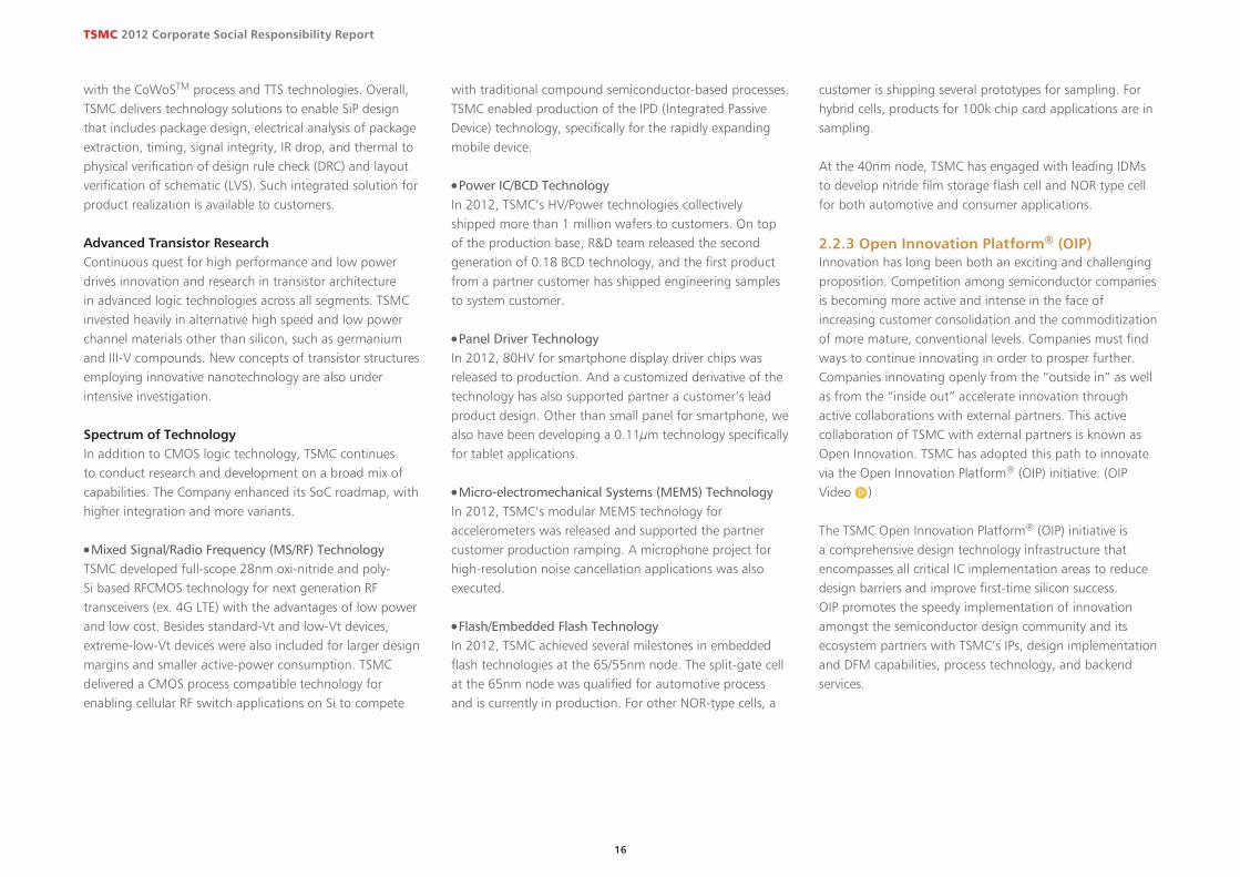
Technology leadership and manufacturing excellence are the bedrock of TSMC’s competitive advantage.
Integrated Interconnect and PackagingIn 2012, TSMC became the world’s first foundry to provide full system integration turn-key solutions to customers. The Company developed and delivered backend technologies starting from advanced back-end-of-line (BEOL) interconnect, to the production-ready fine pitch silicon interposer with through silicon via (TSV) and chip stacking, and all the way to advanced wafer-level-chip scale packaging (WLCSP) including fan-in and fan-out, and ultra fine pitch large die lead-free flip chip packaging. TSMC can offer our customers corresponding design tools, technology, and mass production capability. Such options were made available to customers in 2012. Advanced BEOL interconnection is further refined and extended with innovative damascene processes. And the flip chip packaging technology envelope was expanded to larger chip size and finer bump pitches for advanced technology nodes (28nm and 20nm). Efforts are also made to include fan-in and fan-out wafer level packaging technology in our offerings to customers. The solution has been qualified by selective customers.
● Advanced InterconnectAdvanced interconnects with low resistance/capacitance RC delay continued to be the primary focus of TSMC BEOL technology development in 2012. For 16nm node and beyond, we have developed a new interconnect scheme to achieve minimum pitch and a new metal patterning to minimize resistance/capacitance RC delay.
At the 20nm node, the effective resistivity of our Cu lines is highly competitive and lower than that projected by the International Technology Roadmap for Semiconductors (ITRS).
● Advanced Package DevelopmentTo provide innovative and cost competitive lead-free bumping and packaging solutions in 2012, TSMC developed and qualified 28nm technology node Bump-on-Trace packaging technology with ultra-fine pitch array (100μm pitch) Cu-bump for mobile devices. The Company expanded the lead-free packaging technology envelope to the 20nm node and offered a wide variety of lead-free flip chip packaging technologies for both mobile/handheld and high performance applications to enhance customers’ competitiveness.
● 3D ICIn 2012, R&D completed CoWoSTM process and package qualifications and transferred the technology for production. TSMC’s CoWoSTM solution provides a simple integration process for customers to realize their products with optimized cost and cycle time. We have also developed 3D IC 28HPM through transistor stacking (TTS) technology, that can enable customers for applications requiring small form factor, high performance and low power dissipation. Realizing the critical nature of 3D IC thermal management, TSMC has also developed thermal solutions associated
TSMC 2012 Corporate Social Responsibility Report
16
with the CoWoSTM process and TTS technologies. Overall, TSMC delivers technology solutions to enable SiP design that includes package design, electrical analysis of package extraction, timing, signal integrity, IR drop, and thermal to physical verification of design rule check (DRC) and layout verification of schematic (LVS). Such integrated solution for product realization is available to customers.
Advanced Transistor ResearchContinuous quest for high performance and low power drives innovation and research in transistor architecture in advanced logic technologies across all segments. TSMC invested heavily in alternative high speed and low power channel materials other than silicon, such as germanium and III-V compounds. New concepts of transistor structures employing innovative nanotechnology are also under intensive investigation.
Spectrum of TechnologyIn addition to CMOS logic technology, TSMC continues to conduct research and development on a broad mix of capabilities. The Company enhanced its SoC roadmap, with higher integration and more variants.
● Mixed Signal/Radio Frequency (MS/RF) TechnologyTSMC developed full-scope 28nm oxi-nitride and poly-Si based RFCMOS technology for next generation RF transceivers (ex. 4G LTE) with the advantages of low power and low cost. Besides standard-Vt and low-Vt devices, extreme-low-Vt devices were also included for larger design margins and smaller active-power consumption. TSMC delivered a CMOS process compatible technology for enabling cellular RF switch applications on Si to compete
with traditional compound semiconductor-based processes. TSMC enabled production of the IPD (Integrated Passive Device) technology, specifically for the rapidly expanding mobile device.
● Power IC/BCD TechnologyIn 2012, TSMC’s HV/Power technologies collectively shipped more than 1 million wafers to customers. On top of the production base, R&D team released the second generation of 0.18 BCD technology, and the first product from a partner customer has shipped engineering samples to system customer.
● Panel Driver TechnologyIn 2012, 80HV for smartphone display driver chips was released to production. And a customized derivative of the technology has also supported partner a customer’s lead product design. Other than small panel for smartphone, we also have been developing a 0.11µm technology specifically for tablet applications.
● Micro-electromechanical Systems (MEMS) TechnologyIn 2012, TSMC’s modular MEMS technology for accelerometers was released and supported the partner customer production ramping. A microphone project for high-resolution noise cancellation applications was also executed.
● Flash/Embedded Flash TechnologyIn 2012, TSMC achieved several milestones in embedded flash technologies at the 65/55nm node. The split-gate cell at the 65nm node was qualified for automotive process and is currently in production. For other NOR-type cells, a
customer is shipping several prototypes for sampling. For hybrid cells, products for 100k chip card applications are in sampling.
At the 40nm node, TSMC has engaged with leading IDMs to develop nitride film storage flash cell and NOR type cell for both automotive and consumer applications.
2.2.3 Open Innovation Platform® (OIP)Innovation has long been both an exciting and challenging proposition. Competition among semiconductor companies is becoming more active and intense in the face of increasing customer consolidation and the commoditization of more mature, conventional levels. Companies must find ways to continue innovating in order to prosper further. Companies innovating openly from the “outside in” as well as from the “inside out” accelerate innovation through active collaborations with external partners. This active collaboration of TSMC with external partners is known as Open Innovation. TSMC has adopted this path to innovate via the Open Innovation Platform® (OIP) initiative. (OIP Video )
The TSMC Open Innovation Platform® (OIP) initiative is a comprehensive design technology infrastructure that encompasses all critical IC implementation areas to reduce design barriers and improve first-time silicon success. OIP promotes the speedy implementation of innovation amongst the semiconductor design community and its ecosystem partners with TSMC’s IPs, design implementation and DFM capabilities, process technology, and backend services.
TSMC 2012 Corporate Social Responsibility Report
17
customers to take full advantage of the process technologies once they reach production-ready maturity.
In October 2012, TSMC hosted the OIP Ecosystem Forum at San Jose Convention Center in California, with keynote addresses from the executives of TSMC as well as OIP ecosystem partners. The forum was well attended by both customers and ecosystem partners and demonstrated the value of collaboration through OIP to nurture innovations.
TSMC’s OIP Partner Management Portal facilitates communication with our ecosystem partners for efficient business productivity. This portal is designed with an intuitive interface and can be linked directly from TSMC-Online.
2.2.4 A Vehicle to Make Ideas Come True–Tsmc University Shuttle Program
The TSMC University Shuttle Program was established to handle MPW (Multi-Project Wafer) access requests by qualified professors at leading research universities worldwide. To participating professors, TSMC University Shuttle Program provides annual pre-approved access to quality technologies, including 65nm, 40nm process nodes for analog/mixed-signal circuits and RF design, and 0.11μm/0.18μm process nodes for micro-electromechanical system designs. For very advanced logic design and SRAM researches, the 28nm process node is provided to special university projects. To TSMC, the key performance indices are the 3Rs: Recruiting, Research results transfer from universities to TSMC, and Recognition.
Participation in the TSMC University Shuttle Program include the active participation of major university research groups:
in the U.S., M.I.T., Stanford University, UC Berkeley, Harvard University, and UCLA; in Taiwan, National Taiwan University, National Chiao-Tung University, and National Tsing-Hua University; in China, Tsing Hua University in Beijing, and Hong Kong University of Science and Technology, and in Singapore, Nanyang Technological University.
The TSMC University Shuttle Program serves as an effective bridge to link motivated professors and graduate students in leading research universities worldwide with enthusiastic directors and managers at TSMC to contribute to newer level of excellence in advancing technologies and in nurturing new generations of talent in the semiconductor field.
TSMC’s University Shuttle Program has been very effective and is praised by professors around the world. They recognize that this Program allows their graduate students to implement exciting designs ranging from low-power memories, analog-to-digital converters and digital designs to advanced radio-frequency and mixed-signal bio-medical systems. This is truly “win-win” collaboration. In 2012, TSMC received specific letters of appreciation from professors at M.I.T., Stanford University, UC Berkeley, Harvard University, UCLA, National Taiwan University and National Chiao-Tung University.
A key element of OIP is a set of ecosystem interfaces and collaborative components initiated and supported by TSMC that more efficiently empowers innovation throughout the supply chain and, in turn, drives the creation and sharing of newly-created revenue and profits. TSMC’s Active Accuracy Assurance (AAA) initiative is critical to OIP, providing the accuracy and quality required by the ecosystem interfaces and collaborative components.
TSMC’s Open Innovation model brings together the innovative thinking of customers and partners under the common goal of shortening design time, minimizing time-to-volume, speeding time-to-market and, ultimately, time-to-revenue:● The foundry segment’s largest, most comprehensive and
robust silicon-proven intellectual properties (IPs) and library portfolio;
● Advanced design methodology delivery through reference flows, design for manufacturing (DFM), and process design kits; and
● Comprehensive design ecosystem alliance programs covering market-leading EDA, library, IPs, and design service partners.
TSMC’s OIP Alliance consists of 30 electronic design automation (EDA) partners, 41 IP partners, and 26 design service partners. TSMC and its partners proactively work together, and engage much earlier and deeper than before in order to address mounting design challenges at advanced technology nodes. Through this early and intensive collaboration effort, TSMC OIP is able to deliver the needed design infrastructure with timely enhancement of EDA tools, early availability of critical IPs and quality design services when customers need them. This is critical to success for the
TSMC 2012 Corporate Social Responsibility Report
18
2.2.5 Future R&D PlansIn light of the significant accomplishments of TSMC’s advanced technologies in 2012, the Company plans to continue to grow its R&D investments. The Company plans to reinforce its exploratory development work on new transistors and technologies, such as 3D structures, strained-layer CMOS, high mobility materials and novel 3D IC devices. These studies of the fundamental physics of nanometer CMOS transistors are core aspects of our efforts to improve the understanding and guide the design of transistors at advanced nodes. The findings of these studies are being applied to ensure our continued industry leadership at the 28nm and 20nm nodes and to extend our leadership to the 10nm and 7nm nodes. One of TSMC’s goals is to extend Moore’s Law through both innovative in-house work and by collaborating with industry leaders and academia. We seek to push the envelope in finding cost-effective technologies and manufacturing solutions.
TSMC intends to continue working closely with international consortia and lithography equipment suppliers to ensure the timely development of 193nm high-NA scanner technology, EUV lithography, and massively parallel e-beam direct-write technologies. These technologies are increasingly important to TSMC’s process development efforts at the 10nm, 7nm, and smaller nodes.
TSMC continues to work with mask writing and inspection equipment suppliers to develop viable mask making technology to help ensure that the Company maintains
its leadership position in mask quality & cycle time and continues to meet aggressive R&D, prototyping and production requirements.
With a highly competent and dedicated R&D team, and its unwavering commitment to innovation, TSMC is confident of its ability to deliver the best and most cost-effective SoC technologies for its customers, thereby supporting the Company’s business growth and profitability.
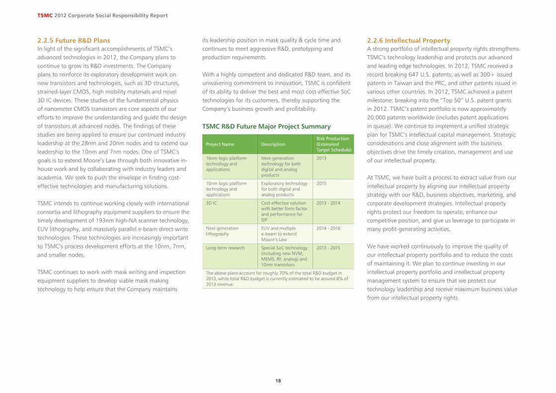
TSMC R&D Future Major Project Summary
Project Name DescriptionRisk Production (Estimated Target Schedule)
16nm logic platform technology and applications
Next-generation technology for both digital and analog products
2013
10nm logic platform technology and applications
Exploratory technology for both digital and analog products
2015
3D IC Cost-effective solution with better form factor and performance for SIP
2013 - 2014
Next-generation lithography
EUV and multiple e-beam to extend Moore’s Law
2014 - 2016
Long-term research Special SoC technology (including new NVM, MEMS, RF, analog) and 10nm transistors
2013 - 2015
The above plans account for roughly 70% of the total R&D budget in 2013, while total R&D budget is currently estimated to be around 8% of 2013 revenue.
2.2.6 Intellectual PropertyA strong portfolio of intellectual property rights strengthens TSMC’s technology leadership and protects our advanced and leading edge technologies. In 2012, TSMC received a record breaking 647 U.S. patents, as well as 300+ issued patents in Taiwan and the PRC, and other patents issued in various other countries. In 2012, TSMC achieved a patent milestone: breaking into the “Top 50” U.S. patent grants in 2012. TSMC’s patent portfolio is now approximately 20,000 patents worldwide (includes patent applications in queue). We continue to implement a unified strategic plan for TSMC’s intellectual capital management. Strategic considerations and close alignment with the business objectives drive the timely creation, management and use of our intellectual property.
At TSMC, we have built a process to extract value from our intellectual property by aligning our intellectual property strategy with our R&D, business objectives, marketing, and corporate development strategies. Intellectual property rights protect our freedom to operate, enhance our competitive position, and give us leverage to participate in many profit-generating activities.
We have worked continuously to improve the quality of our intellectual property portfolio and to reduce the costs of maintaining it. We plan to continue investing in our intellectual property portfolio and intellectual property management system to ensure that we protect our technology leadership and receive maximum business value from our intellectual property rights.
TSMC 2012 Corporate Social Responsibility Report
19
2.3 Trade Secret ProtectionTo protect TSMC’s competitive edge and invaluable intellectual property, the Company is dedicated to Proprietary Information Protection (PIP) (e.g. protection of the trade secrets of TSMC and our customers, etc.), to preserve the interests of the Company, customers, employees and shareholders. We established the TSMC Proprietary Information Protection Policy , which clearly defines PIP management procedures and guidelines.
Training and promotions are rolled out for every employee in TSMC. The Company reinforces employees’ awareness and capability for proprietary information classification and familiarity with handling processes. Regular audits are conducted, as well as annual PIP refresher training for all TSMC employees. In addition, if PIP policy is violated, warnings or punishments will be delivered depending upon severity. Legal action will also be undertaken in certain situations.
TSMC regards vendors as the Company’s important partners, and thus provides security training and management to help them fit in with the Company’s security culture. Each individual vendor must take PIP and work safety training, sign a nondisclosure agreement, and pass a work safety exam before receiving a working badge. TSMC also hosts a security symposium for vendor companies every quarter. During the gathering, vendor companies not only share successful experiences, but also review improvement plans. The symposium successfully helps vendors follow TSMC regulations.
2.4 Membership in Industry AssociationsAs a semiconductor industry leader, TSMC actively participates in trade and industry associations. TSMC executives have been nominated to and hold senior positions in associations including the Taiwan Semiconductor Industry Association, the Association of Industries in Science Parks, the Chinese National Association of Industry and Commerce, the Taiwan Electrical and Electronic Manufacturers’ Association, the Mount Jade Science and Technology Association of Taiwan, and the Taiwan Business Council for Sustainable Development, holding positions such as Chairman or Executive Board Director. In addition, many TSMC employees also contribute to the semiconductor industry and professional associations by serving in industry associations as committee chairman or vice chairman in various committees.
2.5 Investor EngagementTSMC’s business strategies and financial policies aim to uphold and increase shareholder value. We align ourselves with international standards that demonstrate our position and reputation as a sustainability champion, and have been
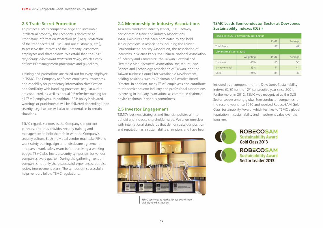
TSMC Leads Semiconductor Sector at Dow Jones Sustainability Indexes (DJSI)
Total Score: 2012 Semiconductor Sector
TSMC Average
Total Score 87 49
Dimensional Score: 2012
Weighting TSMC Average
Economic 40% 85 56
Environmental 35% 91 44
Social 25% 84 45
TSMC continued to receive various awards from globally noted institutions
included as a component of the Dow Jones Sustainability Indexes (DJSI) for the 12th consecutive year since 2001. Furthermore, in 2012, TSMC was recognized as the DJSI Sector Leader among global Semiconductor companies for the second year since 2010 and received RobecoSAM Gold Class Sustainability Award, which testifies to TSMC’s global reputation in sustainability and investment value over the long run.
TSMC 2012 Corporate Social Responsibility Report
20
Since becoming a publicly listed company in 1994, TSMC has consistently delivered value to shareholders through cash dividends and share price appreciation, maintaining a strong balance sheet, and keeping one of the highest credit ratings among global semiconductor companies and Taiwan companies (Standard & Poor’s (S&P) Ratings: A+; Moody’s Ratings: A1; Taiwan Ratings: twAAA). In our core semiconductor business, we invest in opportunities that will expand our leadership in technology and capacity. In 2012, in addition to a record R&D budget of US$1.4 billion, TSMC spent an unprecedented US$8.3 billion on capital expenditures to meet the capacity needs of our customers. Moreover, we actively pursue new revenue opportunities in solid state lighting and thin film solar photovoltaic
Financial Performance - 2002 – 2012 Averaged ROE = 23%; PBT CAGR = 15%
2002 2003 2004 2005 2006 2007 2008 2009 2010 2011 2012
Revenue (NT$ in Billion) Profit before Tax (PBT) (NT$ in Billion) ROE
27162
51203
92257
94267
133317
122323
111333
95296
170420
145427
182506
8%
15%
25%22%
27%
22%21%
18%
30%
22% 25%
Market Capitalization – Over NT$2.5 Trillion
1994 1995 1996 1997 1998 1999 2000 2001 2002 2003 2004 2005 2006 2007 2008 2009 2010 2011 2012
1994/09/05 NT$75 Billion, or US$ 2.9 Billion
2012/12/31 NT$2.5 Trillion, or US$86 Billion
Cash Dividend – Over NT$580 Billion from 2004 to 2012
0.6 2.0 2.5 3.0 3.0 3.0 3.0 3.0 3.0
78 7878
2004 2005 2006 2007 2008 2009 2010 2011 2012
Cash Dividend per Share (NT$) Total Dividend Paid (NT$ Billion)
77 7777
46
62
12
TSMC 2012 Corporate Social Responsibility Report
21
technology, which leverage our technological strengths and engineering capabilities. We believe these investments will fuel TSMC’s future growth and maximize our shareholder value.
In order to serve investors and the investment community, TSMC has established a highly effective communication system to disseminate information. Each quarter, our CEO and CFO jointly hold a face-to-face earnings conference and audio conference call to report and discuss company performance with investors worldwide. Starting from July 2012, TSMC further combines the earnings conference and conference call to allow broader participation to the live event. Replays and transcripts of these conferences are then made available on the company website for investors’ reference. Each year, our Investor Relations team holds hundreds of investor and analyst meetings and conference calls, and actively participates in broker-sponsored investor conferences and non-deal roadshows, extending our reach in Asia, Europe and North America. In 2012, more than 280 such meetings and conference calls were held with investors worldwide. All these efforts are focused on serving worldwide investors with accurate, timely, and transparent information and financial data regarding TSMC business strategy, operations and performance. In addition, E-mail updates covering all business activities and key events are regularly sent to thousands of members of the investment community. Information regarding TSMC’s business fundamentals, analysts’ recommendation summary, credit ratings, and important filings with regulatory authorities is posted on TSMC’s corporate website in a timely manner.
In order to increase shareholders’ value, TSMC has set clear strategic financial objectives. These strategic financial objectives include: (1) average return on equity (ROE) across cycle greater or equal to 20%; (2) 10% profit before tax (PBT) compounded annual growth rate (CAGR) from 2010 to 2015. These financial objectives can help investors better understand TSMC’s long-term investment value, while our financial track record gives investors higher confidence in TSMC’s capability to achieve these financial objectives. For example, during 2002 to 2012, TSMC’s averaged ROE was 23% and CAGR for profit before tax was 15%, both of which met our long-term financial objectives. Supported by solid financial performances, TSMC’s share performance including cash dividends increased 33% during 2012, and significantly outperformed the Taiwan Stock Exchange Capitalization Weighted Stock Index (TAIEX) performance of 9% over the same period. TSMC’s American Depository Receipt performance including cash dividends increased 38%, significantly outperformed the Philadelphia Stock Exchange Semiconductor Index (SOX) performance of 5%. Since the Company went IPO in 1994, TSMC’s market capitalization has grown steadily. As of December 31, 2012, TSMC’s market capitalization reached above NT$2.5 trillion, or US$86 billion.
Starting from 2004, TSMC has distributed cash dividends each year to our shareholders. From 2004 to 2012, TSMC has already paid out more than NT$580 billion, or US$18 billion, in cash dividends. Moreover, TSMC commits to our shareholders that our dividend policy is one that will maintain or steadily increase dividend per share (DPS) every year.
Annual investors surveys conducted by media have recognized the transparency of TSMC’s disclosure policies, corporate governance commitment, and equitable treatment of shareholders. Furthermore, in 2012, TSMC continued to receive various awards from globally noted institutions such as Institutional Investor and IR Magazine. Regarding total awards and recognition in 2012, please refer to “2012 Awards and Recognitions” in page 5.
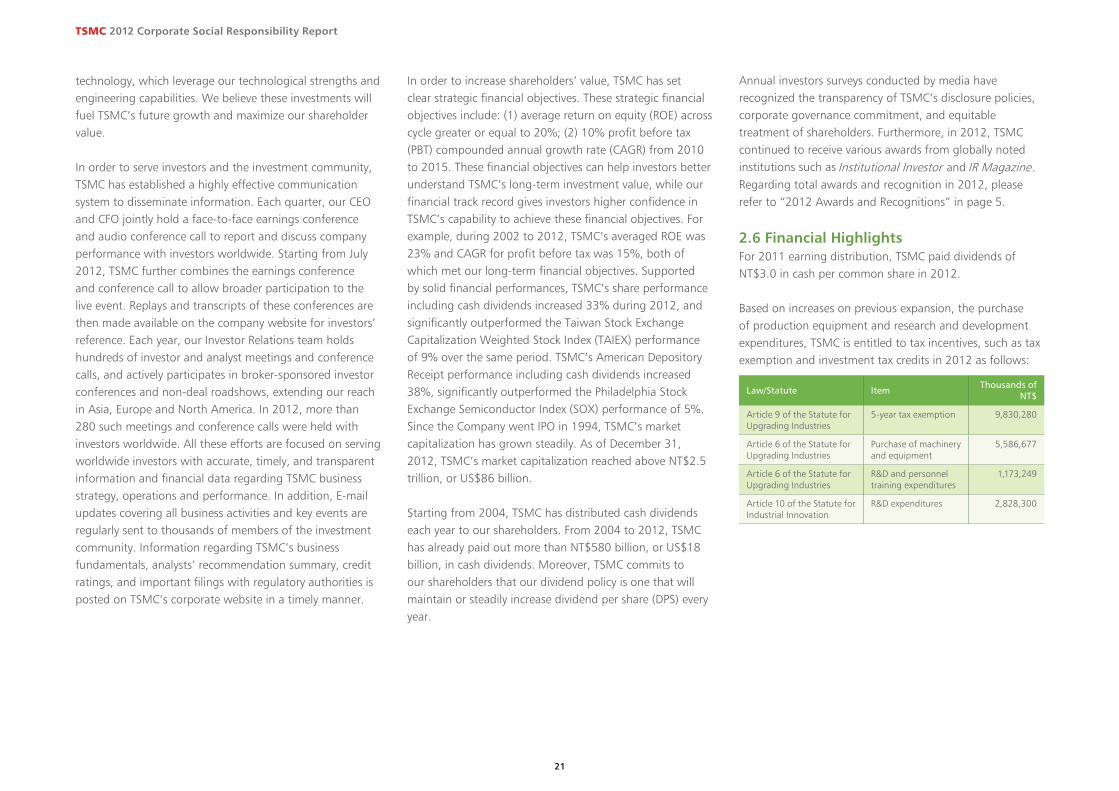
2.6 Financial HighlightsFor 2011 earning distribution, TSMC paid dividends of NT$3.0 in cash per common share in 2012.
Based on increases on previous expansion, the purchase of production equipment and research and development expenditures, TSMC is entitled to tax incentives, such as tax exemption and investment tax credits in 2012 as follows:
Law/Statute ItemThousands of
NT$
Article 9 of the Statute for Upgrading Industries
5-year tax exemption 9,830,280
Article 6 of the Statute for Upgrading Industries
Purchase of machinery and equipment
5,586,677
Article 6 of the Statute for Upgrading Industries
R&D and personnel training expenditures
1,173,249
Article 10 of the Statute for Industrial Innovation
R&D expenditures 2,828,300
TSMC 2012 Corporate Social Responsibility Report
22
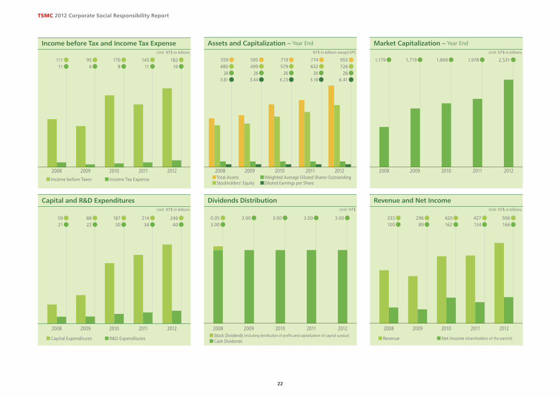
Assets and Capitalization – Year End
2008 2009 2010 2011 2012Total Assets Weighted Average Diluted Shares OutstandingStockholders’ Equity Diluted Earnings per Share
NT$ in billions except EPS
480559
499595
579719 774
632 726955
263.81
263.44
266.23
265.18
266.41
Dividends Distribution
2008 2009 2010 2011 2012Stock Dividends (including distribution of profits and capitalization of capital surplus)Cash Dividends
3.00 3.00 3.00 3.00
Unit: NT$
3.000.05
Market Capitalization – Year End
2008 2009 2010 2011 2012
1,719 1,868 1,978 2,531
Unit: NT$ in billions
1,179
Revenue and Net Income
2008 2009 2010 2011 2012
Revenue Net Income (shareholders of the parent)
100 89 162 134 166333 296 420 427 506
Unit: NT$ in billions
Income before Tax and Income Tax Expense
2008 2009 2010 2011 2012
Income before Taxes Income Tax Expense
11 6 8 11 16111 95 170 145 182
Unit: NT$ in billions
Capital and R&D Expenditures
2008 2009 2010 2011 2012
Capital Expenditures R&D Expenditures
21 22 30 34 4059 88 187 214 246
Unit: NT$ in billions