Embed Size (px)
Citation preview

24AA32A/24LC32A32K I2C™ Serial EEPROM
Device Selection Table
Features:• Single Supply with Operation down to 1.7V for
24AA32A Devices, 2.5V for 24LC32A Devices• Low-Power CMOS Technology:
- Active current 1 mA, typical- Standby current 1 A, typical
• 2-Wire Serial Interface, I2C™ Compatible• Schmitt Trigger Inputs for Noise Suppression• Output Slope Control to Eliminate Ground Bounce• 100 kHz and 400 kHz Clock Compatibility• Page Write Time 5 ms max.• Self-Timed Erase/Write Cycle• 32-Byte Page Write Buffer• Hardware Write-Protect• ESD Protection > 4,000V• More than 1 Million Erase/Write Cycles• Data Retention > 200 Years• Factory Programming Available• Packages Include 8-lead PDIP, SOIC, SOIJ,
TSSOP, X-Rotated TSSOP, MSOP, DFN, TDFN, 5-lead SOT-23 and Chip Scale
• Pb-Free and RoHS Compliant• Temperature Ranges:
- Industrial (I): -40°C to +85°C- Automotive (E): -40°C to +125°C
Description:The Microchip Technology Inc. 24AA32A/24LC32A (24XX32A*) is a 32 Kbit Electrically Erasable PROM. The device is organized as a single block of 4K x 8-bit memory with a 2-wire serial interface. Low-voltage design permits operation down to 1.7V, with standby and active currents of only 1 A and 1 mA, respectively. It has been developed for advanced, low-power applications such as personal communications or data acquisition. The 24XX32A also has a page write capability for up to 32 bytes of data. Functional address lines allow up to eight devices on the same bus, for up to 256 Kbits address space. The 24XX32A is available in the standard 8-pin PDIP, surface mount SOIC, SOIJ, TSSOP, DFN, TDFN and MSOP packages. The 24XX32A is also available in the 5-lead SOT-23 and Chip Scale packages.
Block Diagram
Package Types
Part Number
VCC Range
Max. Clock Frequency
Temp. Ranges
24AA32A 1.7-5.5 400 kHz(1) I24LC32A 2.5-5.5 400 kHz I, ENote 1: 100 kHz for VCC <2.5V.
HV Generator
EEPROM Array
Page Latches
YDEC
XDEC
Sense Amp.R/W Control
I/OControl
Logic
I/O
MemoryControlLogic
A0 A1 WPA2
SCL
SDA
VccVSS
A0
A1
A2
VSS
VCC
WP
SCL
SDA
1
2
3
4
8
7
6
5
PDIP/MSOP/SOIC/SOIJ/TSSOP DFN/TDFN
A0
A1A2
VSS
WPSCL
SDA
VCC8765
1
234
SOT-23
1
2
3 4
5 WP
VCC
SCL
VSS
SDA
CS (Chip Scale)(1)
1 23
4 5
VCC
WPSDASCL
VSS
(Top Down View,Balls Not Visible)
Note 1: Available in I-temp, “AA” only.
X-Rotated TSSOP
WPVCC
A0A1
1234
8765
SCLSDAVSSA2
(X/ST)
*24XX32A is used in this document as a generic part number for the 24AA32A/24LC32A devices.
2002-2012 Microchip Technology Inc. DS21713M-page 1

24AA32A/24LC32A
1.0 ELECTRICAL CHARACTERISTICS
Absolute Maximum Ratings (†)
VCC.............................................................................................................................................................................6.5V
All inputs and outputs w.r.t. VSS ......................................................................................................... -0.3V to VCC +1.0V
Storage temperature ...............................................................................................................................-65°C to +150°C
Ambient temperature with power applied................................................................................................-40°C to +125°C
ESD protection on all pins 4 kV
TABLE 1-1: DC CHARACTERISTICS
† NOTICE: Stresses above those listed under “Absolute Maximum Ratings” may cause permanent damage to the device. This is a stress rating only and functional operation of the device at those or any other conditions above those indicated in the operational listings of this specification is not implied. Exposure to maximum rating conditions for extended periods may affect device reliability.
DC CHARACTERISTICS Industrial (I): TA = -40°C to +85°C, VCC = +1.7V to +5.5VAutomotive (E): TA = -40°C to +125°C, VCC = +2.5V to +5.5V
Param.No. Symbol Characteristic Min. Typ. Max. Units Conditions
D1 — A0, A1, A2, WP, SCL and SDA pins
— — — — —
D2 VIH High-level input voltage 0.7 VCC — — V —D3 VIL Low-level input voltage — — 0.3 VCC
0.2 VCCVV
VCC 2.5VVCC < 2.5V
D4 VHYS Hysteresis of SchmittTrigger inputs (SDA, SCL pins)
0.05 VCC — — V VCC 2.5V (Note 1)
D5 VOL Low-level output voltage — — 0.40 V IOL = 3.0 mA, VCC = 4.5VIOL = 2.1 mA, Vcc = 2.5V
D6 ILI Input leakage current — — ±1 A VIN = VSS or VCC
D7 ILO Output leakage current — — ±1 A VOUT = VSS or VCC
D8 CIN, COUT
Pin capacitance(all inputs/outputs)
— — 10 pF VCC = 5.0V (Note 1)TA = 25°C, FCLK = 1 MHz
D9 ICC write Operating current — 0.1 3 mA VCC = 5.5V, SCL = 400 kHzD10 ICC read — 0.05 400 AD11 ICCS Standby current —
—0.01—
15
AA
IndustrialAutomotiveSDA = SCL = VCC = 5.5VA0, A1, A2, WP = VSS
Note 1: This parameter is periodically sampled and not 100% tested.2: Typical measurements taken at room temperature.
DS21713M-page 2 2002-2012 Microchip Technology Inc.

24AA32A/24LC32A
TABLE 1-2: AC CHARACTERISTICSAC CHARACTERISTICS Industrial (I): TA = -40°C to +85°C, VCC = +1.7V to +5.5VAutomotive (E): TA = -40°C to +125°C, VCC = +2.5V to +5.5V
Param.No. Symbol Characteristic Min. Max. Units Conditions
1 FCLK Clock Frequency ——
400100
kHz 2.5V VCC 5.5V1.7V VCC 2.5V (24AA32A)
2 THIGH Clock High Time 6004000
——
ns 2.5V VCC 5.5V1.7V VCC 2.5V (24AA32A)
3 TLOW Clock Low Time 13004700
——
ns 2.5V VCC 5.5V1.7V VCC 2.5V (24AA32A)
4 TR SDA and SCL Rise Time (Note 1)
——
3001000
ns 2.5V VCC 5.5V 1.7V VCC 2.5V (24AA32A)
5 TF SDA and SCL Fall Time — 300 ns (Note 1)6 THD:STA Start Condition Hold Time 600
4000——
ns 2.5V VCC 5.5V1.7V VCC 2.5V (24AA32A)
7 TSU:STA Start Condition Setup Time 6004700
——
ns 2.5V VCC 5.5V1.7V VCC 2.5V (24AA32A)
8 THD:DAT Data Input Hold Time 0 — ns (Note 2)9 TSU:DAT Data Input Setup Time 100
250——
ns 2.5V VCC 5.5V1.7V VCC 2.5V (24AA32A)
10 TSU:STO Stop Condition Setup Time 6004000
——
ns 2.5V VCC 5.5V1.7V VCC 2.5V (24AA32A)
11 TSU:WP WP Setup Time 6004000
——
ns 2.5V VCC 5.5V1.7V VCC < 2.5V (24AA32A)
12 THD:WP WP Hold Time 13004700
——
ns 2.5V VCC 5.5V1.7V VCC < 2.5V (24AA32A)
13 TAA Output Valid from Clock (Note 2)
——
9003500
ns 2.5V VCC 5.5V1.7V VCC 2.5V (24AA32A)
14 TBUF Bus free time: Time the bus must be free before a new transmission can start
13004700
——
ns 2.5V VCC 5.5V1.7V VCC 2.5V (24AA32A)
15 TOF Output Fall Time from VIH Minimum to VIL Maximum
20+0.1CB—
250250
ns 2.5V VCC 5.5V1.7V VCC 2.5V (24AA32A)
16 TSP Input Filter Spike Suppression(SDA and SCL pins)
— 50 ns (Notes 1 and 3)
17 TWC Write Cycle Time (byte or page)
— 5 ms —
18 — Endurance 1M — cycles Page mode, 25°C, VCC 5.5V (Note 4)
Note 1: Not 100% tested. CB = total capacitance of one bus line in pF.2: As a transmitter the device must provide an internal minimum delay time to bridge the undefined region
(minimum 300 ns) of the falling edge of SCL to avoid unintended generation of Start or Stop conditions.3: The combined TSP and VHYS specifications are due to new Schmitt Trigger inputs which provide improved
noise spike suppression. This eliminates the need for a TI specification for standard operation.4: This parameter is not tested but ensured by characterization. For endurance estimates in a specific
application, please consult the Total Endurance™ Model which can be obtained on Microchip’s web site at www.microchip.com.
2002-2012 Microchip Technology Inc. DS21713M-page 3

24AA32A/24LC32A
FIGURE 1-1: BUS TIMING DATAFIGURE 1-2: BUS TIMING START/STOP
(unprotected)(protected)
SCL
SDAIN
SDAOUT
WP
5
7
6
16
3
2
8 9
13
D4 4
10
11 12
14
76
D4
10
Start Stop
SCL
SDA
DS21713M-page 4 2002-2012 Microchip Technology Inc.

24AA32A/24LC32A
2.0 PIN DESCRIPTIONSThe descriptions of the pins are listed in Table 2-1.
TABLE 2-1: PIN FUNCTION TABLE
2.1 A0, A1, A2 Chip Address InputsThe A0, A1 and A2 inputs are used by the 24XX32A for multiple device operation. The levels on these inputs are compared with the corresponding bits in the slave address. The chip is selected if the comparison is true.
Up to eight devices may be connected to the same bus by using different Chip Select bit combinations. These inputs must be connected to either VCC or VSS.
In most applications, the chip address inputs A0, A1 and A2 are hard-wired to logic ‘0’ or logic ‘1’. For applications in which these pins are controlled by a microcontroller or other programmable device, the chip address pins must be driven to logic ‘0’ or logic ‘1’ before normal device operation can proceed. Address pins are not available in the SOT-23 and chip scale packages.
2.2 Serial Data (SDA)SDA is a bidirectional pin used to transfer addresses and data into and out of the device. It is an open-drain terminal, therefore, the SDA bus requires a pull-up resistor to VCC (typical 10 k for 100 kHz, 2 k for 400 kHz)
For normal data transfer, SDA is allowed to change only during SCL low. Changes during SCL high are reserved for indicating Start and Stop conditions.
2.3 Serial Clock (SCL)The SCL input is used to synchronize the data transfer to and from the device.
2.4 Write-Protect (WP)This pin must be connected to either VSS or VCC. If tied to VSS, write operations are enabled. If tied to VCC, write operations are inhibited but read operations are not affected.
Name PDIP SOIC SOIJ TSSOP Rotated TSSOP DFN(1) TDFN(1) MSOP SOT-23 CS Description
A0 1 1 1 1 3 1 1 1 — — Chip Address InputA1 2 2 2 2 4 2 2 2 — — Chip Address InputA2 3 3 3 3 5 3 3 3 — — Chip Address InputVSS 4 4 4 4 6 4 4 4 2 2 GroundSDA 5 5 5 5 7 5 5 5 3 5 Serial Address/Data I/OSCL 6 6 6 6 8 6 6 6 1 4 Serial ClockWP 7 7 7 7 1 7 7 7 5 3 Write-Protect InputVCC 8 8 8 8 2 8 8 8 4 1 +1.7V to 5.5V Power SupplyNote 1: The exposed pad on the DFN/TDFN packages can be connected to VSS or left floating.
2002-2012 Microchip Technology Inc. DS21713M-page 5

24AA32A/24LC32A
3.0 FUNCTIONAL DESCRIPTIONThe 24XX32A supports a bidirectional, 2-wire bus and data transmission protocol. A device that sends data onto the bus is defined as transmitter, while a device receiving data is defined as a receiver. The bus has to be controlled by a master device which generates the Serial Clock (SCL), controls the bus access and gener-ates the Start and Stop conditions, while the 24XX32A works as slave. Both master and slave can operate as transmitter or receiver, but the master device determines which mode is activated.
4.0 BUS CHARACTERISTICSThe following bus protocol has been defined:
• Data transfer may be initiated only when the bus is not busy.
• During data transfer, the data line must remain stable whenever the clock line is high. Changes in the data line while the clock line is high will be interpreted as a Start or Stop condition.
Accordingly, the following bus conditions have been defined (Figure 4-1).
4.1 Bus Not Busy (A)Both data and clock lines remain high.
4.2 Start Data Transfer (B)A high-to-low transition of the SDA line while the clock (SCL) is high determines a Start condition. All commands must be preceded by a Start condition.
4.3 Stop Data Transfer (C)A low-to-high transition of the SDA line while the clock (SCL) is high determines a Stop condition. All operations must be ended with a Stop condition.
4.4 Data Valid (D)The state of the data line represents valid data when, after a Start condition, the data line is stable for the duration of the high period of the clock signal.
The data on the line must be changed during the low period of the clock signal. There is one clock pulse per bit of data.
Each data transfer is initiated with a Start condition and terminated with a Stop condition. The number of data bytes transferred between Start and Stop conditions is determined by the master device and is, theoretically,unlimited (although only the last thirty-two bytes will be stored when doing a write operation). When an over-write does occur, it will replace data in a first-in first-out (FIFO) fashion.
4.5 AcknowledgeEach receiving device, when addressed, is obliged to generate an Acknowledge after the reception of each byte. The master device must generate an extra clock pulse which is associated with this Acknowledge bit.
The device that acknowledges, has to pull down the SDA line during the Acknowledge clock pulse in such a way that the SDA line is stable low during the high period of the Acknowledge related clock pulse. Of course, setup and hold times must be taken into account. During reads, a master must signal an end of data to the slave by not generating an Acknowledge bit on the last byte that has been clocked out of the slave. In this case, the slave (24XX32A) will leave the data line high to enable the master to generate the Stop condition.
FIGURE 4-1: DATA TRANSFER SEQUENCE ON THE SERIAL BUS
Note: The 24XX32A does not generate any Acknowledge bits if an internal programming cycle is in progress.
SCL
SDA
(A) (B) (D) (D) (A)(C)
StartCondition
Address orAcknowledge
Valid
DataAllowed
to Change
StopCondition
DS21713M-page 6 2002-2012 Microchip Technology Inc.

24AA32A/24LC32A
5.0 DEVICE ADDRESSING A control byte is the first byte received following the Start condition from the master device (Figure 5-1). The control byte consists of a four-bit control code. For the 24XX32A, this is set as ‘1010’ binary for read and write operations. The next three bits of the control byte are the Chip Select bits (A2, A1, A0). The Chip Select bits allow the use of up to eight 24XX32A devices on the same bus and are used to select which device is accessed. The Chip Select bits in the control byte must correspond to the logic levels on the corresponding A2, A1 and A0 pins for the device to respond. These bits are in effect the three Most Significant bits of the word address.
For the SOT-23 and chip scale packages, the address pins are not available. During device addressing, the A1, A2, and A0 Chip Selects bits (Figure 5-2) should be set to ‘0’.
The last bit of the control byte defines the operation to be performed. When set to a ‘1’, a read operation is selected. When set to a zero, a write operation is selected. The next two bytes received define the address of the first data byte (Figure 5-2). Because only A11 to A0 are used, the upper four address bits are “don’t care” bits. The upper address bits are transferred first, followed by the Less Significant bits.
Following the Start condition, the 24XX32A monitors the SDA bus checking the device type identifier being transmitted and, upon receiving a ‘1010’ code and appropriate device select bits, the slave device outputs
an Acknowledge signal on the SDA line. Depending on the state of the R/W bit, the 24XX32A will select a read or write operation.
FIGURE 5-1: CONTROL BYTE FORMAT
5.1 Contiguous Addressing Across Multiple Devices
The Chip Select bits A2, A1 and A0 can be used to expand the contiguous address space for up to 256K bits by adding up to eight 24XX32A devices on the same bus. In this case, software can use A0 of the con-trol byte as address bit A12; A1 as address bit A13; and A2 as address bit A14. It is not possible to sequentially read across device boundaries.
The SOT-23 and chip scale packages do not support multiple device addressing on the same bus.
FIGURE 5-2: ADDRESS SEQUENCE BIT ASSIGNMENTS
1 0 1 0 A2 A1 A0S ACKR/W
Control CodeChip Select
Bits
Slave Address
Acknowledge BitStart Bit
Read/Write Bit
1 0 1 0 A2
A1
A0 R/W x x x x A
11A10
A9
A7
A0
A8 • • • • • •
Control Byte Address High Byte Address Low Byte
ControlCode
ChipSelect
Bitsx = “don’t care” bit
2002-2012 Microchip Technology Inc. DS21713M-page 7

24AA32A/24LC32A
6.0 WRITE OPERATIONS
6.1 Byte WriteFollowing the Start condition from the master, the control code (4 bits), the Chip Select (3 bits), and the R/W bit (which is a logic low) are clocked onto the bus by the master transmitter. This indicates to the addressed slave receiver that the address high byte will follow once it has generated an Acknowledge bit during the ninth clock cycle. Therefore, the next byte transmitted by the master is the high-order byte of the word address and will be written into the Address Pointer of the 24XX32A. The next byte is the Least Significant Address Byte. After receiving another Acknowledge signal from the 24XX32A, the master device will transmit the data word to be written into the addressed memory location. The 24XX32A acknowl-edges again and the master generates a Stop condition. This initiates the internal write cycle and, during this time, the 24XX32A will not generate Acknowledge signals (Figure 6-1). If an attempt is made to write to the array with the WP pin held high, the device will acknowledge the command, but no write cycle will occur. No data will be written and the device will immediately accept a new command. After a byte Write command, the internal address counter will point to the address location following the one that was just written.
6.2 Page Write The write control byte, word address and the first data byte are transmitted to the 24XX32A in the same way as in a byte write. However, instead of generating a Stop condition, the master transmits up to 31 additional bytes which are temporarily stored in the on-chip page buffer and will be written into memory once the master has transmitted a Stop condition. Upon receipt of each word, the five lower Address Pointer bits are internally incremented by ‘1’. If the master should transmit more than 32 bytes prior to generating the Stop condition, the address counter will roll over and the previously received data will be overwritten. As with the byte write operation, once the Stop condition is received, an internal write cycle will begin (Figure 6-2). If an attempt is made to write to the array with the WP pin held high, the device will acknowledge the command, but no write cycle will occur, no data will be written, and the device will immediately accept a new command.
6.3 Write ProtectionThe WP pin allows the user to write-protect the entire array (000-FFF) when the pin is tied to VCC. If tied to VSS the write protection is disabled. The WP pin is sampled at the Stop bit for every Write command (Figure 4-1). Toggling the WP pin after the Stop bit will have no effect on the execution of the write cycle.
Note: When doing a write of less than 32 bytes the data in the rest of the page is refreshed along with the data bytes being written. This will force the entire page to endure a write cycle, for this reason endurance is specified per page.
Note: Page write operations are limited to writing bytes within a single physical page, regardless of the number of bytes actually being written. Physical page boundaries start at addresses that are integer multiples of the page buffer size (or ‘page size’) and end at addresses that are integer multiples of [page size – 1]. If a Page Write command attempts to write across a physical page boundary, the result is that the data wraps around to the beginning of the current page (overwriting data previously stored there), instead of being written to the next page as might be expected. It is therefore necessary for the application software to prevent page write operations that would attempt to cross a page boundary.
DS21713M-page 8 2002-2012 Microchip Technology Inc.

24AA32A/24LC32A
FIGURE 6-1: BYTE WRITEFIGURE 6-2: PAGE WRITE
x x x
Bus ActivityMaster
SDA Line
Bus Activity
START
ControlByte
AddressHigh Byte
AddressLow Byte Data
STOP
ACK
ACK
ACK
ACK
x = “don’t care” bit
S 1 0 1 0 0A2
A1
A0 Px
x x x
Bus ActivityMaster
SDA Line
Bus Activity
START
ControlByte
AddressHigh Byte
AddressLow Byte Data Byte 0
STOP
ACK
ACK
ACK
ACK
Data Byte 31
ACK
x = “don’t care” bit
S 1 0 1 0 0A2
A1
A0 Px
2002-2012 Microchip Technology Inc. DS21713M-page 9

24AA32A/24LC32A
7.0 ACKNOWLEDGE POLLINGSince the device will not acknowledge during a write cycle, this can be used to determine when the cycle is complete (this feature can be used to maximize bus throughput). Once the Stop condition for a Write command has been issued from the master, the device initiates the internally-timed write cycle. ACK polling can then be initiated immediately. This involves the master sending a Start condition followed by the control byte for a Write command (R/W = 0). If the device is still busy with the write cycle, then no ACK will be returned. If no ACK is returned, the Start bit and control byte must be re-sent. If the cycle is complete, the device will return the ACK and the master can then proceed with the next Read or Write command. See Figure 7-1 for flow diagram of this operation.
FIGURE 7-1: ACKNOWLEDGE POLLING FLOW
SendWrite Command
Send StopCondition to
Initiate Write Cycle
Send Start
Send Control Bytewith R/W = 0
Did DeviceAcknowledge
(ACK = 0)?
NextOperation
No
Yes
DS21713M-page 10 2002-2012 Microchip Technology Inc.

24AA32A/24LC32A
8.0 READ OPERATIONRead operations are initiated in the same way as write operations, with the exception that the R/W bit of the control byte is set to ‘1’. There are three basic types of read operations: current address read, random read and sequential read.
8.1 Current Address ReadThe 24XX32A contains an address counter that main-tains the address of the last word accessed, internally incremented by ‘1’. Therefore, if the previous read access was to address ‘n’ (n is any legal address), the next current address read operation would access data from address n + 1.
Upon receipt of the control byte with R/W bit set to ‘1’, the 24XX32A issues an acknowledge and transmits the 8-bit data word. The master will not acknowledge the transfer, but does generate a Stop condition and the 24XX32A discontinues transmission (Figure 8-1).
8.2 Random ReadRandom read operations allow the master to access any memory location in a random manner. To perform this type of read operation, the word address must first be set. This is accomplished by sending the word address to the 24XX32A as part of a write operation (R/W bit set to ‘0’). Once the word address is sent, the master generates a Start condition following the acknowledge. This terminates the write operation, but not before the internal Address Pointer is set. The master issues the control byte again, but with the R/Wbit set to a ‘1’. The 24XX32A will then issue an acknowledge and transmit the 8-bit data word. The master will not acknowledge the transfer, but does generate a Stop condition which causes the 24XX32A to discontinue transmission (Figure 8-2). After a random Read command, the internal address counter will point to the address location following the one that was just read.
8.3 Sequential ReadSequential reads are initiated in the same way as a random read, except that once the 24XX32A transmits the first data byte, the master issues an acknowledge as opposed to the Stop condition used in a random read. This acknowledge directs the 24XX32A to transmit the next sequentially addressed 8-bit word (Figure 8-3). Following the final byte transmitted to the master, the master will NOT generate an acknowledge, but will generate a Stop condition. To provide sequen-tial reads, the 24XX32A contains an internal Address Pointer which is incremented by ‘1’ upon completion of each operation. This Address Pointer allows the entire memory contents to be serially read during one operation. The internal Address Pointer will automati-cally roll over from address FFF to address 000 if the master acknowledges the byte received from the array address FFF.
FIGURE 8-1: CURRENT ADDRESS READ
S P
Bus ActivityMaster
SDA Line
Bus Activity
STOP
ControlByte Data (n)
ACK
NO ACK
START
2002-2012 Microchip Technology Inc. DS21713M-page 11

24AA32A/24LC32A
FIGURE 8-2: RANDOM READFIGURE 8-3: SEQUENTIAL READ
x x x
Bus Activity Master
SDA Line
Bus ActivityACK
NOACK
ACK
ACK
ACK
STOP
START
ControlByte
AddressHigh Byte
AddressLow Byte
ControlByte
DataByte
START
x = “don’t care” bit
S 1 0 1 0 A A A 02 1 0 S 1 0 1 0 A A A12 1 0 Px
Bus ActivityMaster
SDA Line
Bus Activity
ControlByte Data n Data n + 1 Data n + 2 Data n + x
NOACK
ACK
ACK
ACK
ACK
STOPP
DS21713M-page 12 2002-2012 Microchip Technology Inc.

24AA32A/24LC32A
9.0 PACKAGING INFORMATION9.1 Package Marking Information
XXXXXXXXT/XXXNNN
YYWW
8-Lead PDIP (300 mil) Example:
8-Lead SOIC (3.90 mm) Example:
XXXXXXXTXXXXYYWW
NNN
8-Lead TSSOP Example:
24LC32AI/P 13F
0527
24LC32AISN 0527
13F
4LAI52713F
8-Lead MSOP Example:
XXXXXTYWWNNN
4L32AI52713F
8-Lead SOIC (5.28 mm) Example:
XXXXXXXXT/XXXXXXYYWWNNN
24LC32AI/SM
052713F
XXXXTYWWNNN
3e
3e
8-Lead 2x3 DFN Example:
26452713
XXXYWWNN
3e
2002-2012 Microchip Technology Inc. DS21713M-page 13

24AA32A/24LC32A
Part Number1st Line Marking Codes
TSSOP TSSOPX-Rotated
MSOP DFN TDFN SOT-23I Temp. E Temp. I Temp. E Temp. I Temp. E Temp.
24AA32A 4AA 4AAX 4A32AT 261 — A61 — B6NN —24LC32A 4LA 4LAX 4L32AT 264 265 A64 A65 M6NN N6NN
Note: T = Temperature grade (I, E).
8-Lead 2x3 TDFN Example:
A64527I3
XXXYWWNN
5-Lead SOT-23 Example:
XXNN M6NN
5-Lead Chip Scale
XW
Example:
67
DS21713M-page 14 2002-2012 Microchip Technology Inc.

24AA32A/24LC32A
Legend: XX...X Part number or part number codeT Temperature (I, E)Y Year code (last digit of calendar year)YY Year code (last 2 digits of calendar year)WW Week code (week of January 1 is week ‘01’)NNN Alphanumeric traceability code (2 characters for small packages)
Pb-free JEDEC designator for Matte Tin (Sn)
Note: For very small packages with no room for the Pb-free JEDEC designator , the marking will only appear on the outer carton or reel label.
Note: In the event the full Microchip part number cannot be marked on one line, it will be carried over to the next line, thus limiting the number of available characters for customer-specific information.
3e
3e
Note: Please visit www.microchip.com/Pbfree for the latest information on Pb-free conversion.*Standard OTP marking consists of Microchip part number, year code, week code, and traceability code.
2002-2012 Microchip Technology Inc. DS21713M-page 15

24AA32A/24LC32A
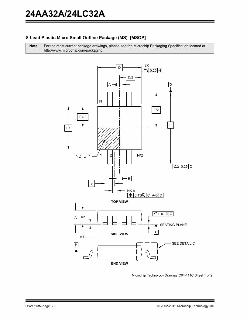
���������� ���������� ������������� ����������
�������� ������ �!"�����#�$�%��&"��'��� ��(�)"&�'"!&�)�����&�#�*�&��&�����&���#������� +������%����&�,����&��!&���-� ��'��!��!�����#�.��#��&�����"#��'�#�%��!����&"!��!����#�%��!����&"!��!�!������&��$���#�����/����!�#���� ��'��!��������#�&���������������.�0������
1�,2�1�!�����'��!���� ���&��������$��&� ��"��!�*��*�&�"&�&������!�
����� 3�&���'!&��"��&����4����#�*���!(�����!��!���&��������������4�����������%���&������&�#��&��&&�255***�'��������'5���4�����
6��&! �7,8.���'��!���9�'�&! ��7 7:� ��;
7"')��%����! 7 <��&�� � �����1�, ��&����&��������� � = = ������#�#����4���� ���4��!! �� ���� ��-� ����1�!��&����&��������� �� ���� = =��"�#��&���"�#��>�#&� . ���� �-�� �-����#�#����4����>�#&� .� ���� ���� ��<�: �����9���&� � �-�< �-?� ���� ���&����&��������� 9 ���� ��-� ����9��#� ���4��!! � ���< ���� ����6����9��#�>�#&� )� ���� ��?� ����9*��9��#�>�#&� ) ���� ���< ����: ������*����������+ �1 = = ��-�
N
E1
NOTE 1
D
1 2 3
A
A1
A2
L
b1b
e
E
eB
c
������� ������� ��*��� ,�����<1
DS21713M-page 16 2002-2012 Microchip Technology Inc.

24AA32A/24LC32A
Note: For the most current package drawings, please see the Microchip Packaging Specification located at http://www.microchip.com/packaging
2002-2012 Microchip Technology Inc. DS21713M-page 17

24AA32A/24LC32A
Note: For the most current package drawings, please see the Microchip Packaging Specification located at http://www.microchip.com/packaging
DS21713M-page 18 2002-2012 Microchip Technology Inc.

24AA32A/24LC32A
���������� �� ���!�� ���� �������""�#$��%&����������� !�'�
����� 3�&���'!&��"��&����4����#�*���!(�����!��!���&��������������4�����������%���&������&�#��&��&&�255***�'��������'5���4�����
2002-2012 Microchip Technology Inc. DS21713M-page 19

24AA32A/24LC32A
Note: For the most current package drawings, please see the Microchip Packaging Specification located at http://www.microchip.com/packaging
DS21713M-page 20 2002-2012 Microchip Technology Inc.

24AA32A/24LC32A
Note: For the most current package drawings, please see the Microchip Packaging Specification located at http://www.microchip.com/packaging
2002-2012 Microchip Technology Inc. DS21713M-page 21

24AA32A/24LC32A
Note: For the most current package drawings, please see the Microchip Packaging Specification located at http://www.microchip.com/packaging
DS21713M-page 22 2002-2012 Microchip Technology Inc.

24AA32A/24LC32A
���������� ��() �� )" �*� ���!�� ���� (����+%+����������( !�
�������� ������ �!"�����#�$�%��&"��'��� ��(�)"&�'"!&�)�����&�#�*�&����&�����&���#������� ��'��!��!�����#�.��#��&�����"#��'�#�%��!����&"!��!����#�%��!����&"!��!�!������&��$���#������''����!�#��-� ��'��!��������#�&���������������.�0������
1�,2 1�!�����'��!���� ���&��������$��&� ��"��!�*��*�&�"&�&������!��.32 ��%��������'��!��(�"!"�����*�&�"&�&������(�%���%'�&����"�!�!�����
����� 3�&���'!&��"��&����4����#�*���!(�����!��!���&��������������4�����������%���&������&�#��&��&&�255***�'��������'5���4�����
6��&! ��99��. .����'��!���9�'�&! ��7 7:� ��;
7"')��%����! 7 <��&�� � ��?��1�,: �����8����& � = = ������#�#����4���� ���4��!! �� ��<� ���� �����&��#%%� �� ���� = ����: �����>�#&� . ?����1�,��#�#����4����>�#&� .� ��-� ���� ������#�#����4����9���&� � ���� -��� -���3&�9���&� 9 ���� ��?� ����3&���& 9� ������.33&������ � �R = <R9��#� ���4��!! � ���� = ����9��#�>�#&� ) ���� = ��-�
D
N
E
E1
NOTE 1
1 2
be
cA
A1
A2
L1 L
φ
������� ������� ��*��� ,����<?1
2002-2012 Microchip Technology Inc. DS21713M-page 23

24AA32A/24LC32A
Note: For the most current package drawings, please see the Microchip Packaging Specification located at http://www.microchip.com/packaging
DS21713M-page 24 2002-2012 Microchip Technology Inc.

24AA32A/24LC32A
���������� ������,��$�����������*�-���.'����/0�0�%&�����������,��
�������� ������ �!"�����#�$�%��&"��'��� ��(�)"&�'"!&�)�����&�#�*�&����&�����&���#������� ���4����'����� ������'���$�!�#�&���)�!��&���#!�-� ���4�����!�!�*�!���"��&�#��� ��'��!��������#�&���������������.�0������
1�,2 1�!�����'��!���� ���&��������$��&� ��"��!�*��*�&�"&�&������!��.32 ��%��������'��!��(�"!"�����*�&�"&�&������(�%���%'�&����"�!�!�����
����� 3�&���'!&��"��&����4����#�*���!(�����!��!���&��������������4�����������%���&������&�#��&��&&�255***�'��������'5���4�����
6��&! ��99��. .����'��!���9�'�&! ��7 7:� ��;
7"')��%����! 7 <��&�� � �����1�,: �����8����& � ��<� ���� �����&��#%%� �� ���� ���� ����,�&��&� ���4��!! �- ������.3: �����9���&� � �����1�,: �����>�#&� . -����1�,.$�!�#���#�9���&� �� ��-� = ����.$�!�#���#�>�#&� .� ���� = ����,�&��&�>�#&� ) ���� ���� ��-�,�&��&�9���&� 9 ��-� ���� ����,�&��&�&�.$�!�#���# U ���� = =
D
N
E
NOTE 1
1 2
EXPOSED PAD
NOTE 12 1
D2
K
L
E2
N
eb
A3 A1
A
NOTE 2
BOTTOM VIEWTOP VIEW
������� ������� ��*��� ,�����-,
2002-2012 Microchip Technology Inc. DS21713M-page 25

24AA32A/24LC32A
Note: For the most current package drawings, please see the Microchip Packaging Specification located at http://www.microchip.com/packaging
DS21713M-page 26 2002-2012 Microchip Technology Inc.

24AA32A/24LC32A
Note: For the most current package drawings, please see the Microchip Packaging Specification located at http://www.microchip.com/packaging
2002-2012 Microchip Technology Inc. DS21713M-page 27

24AA32A/24LC32A
Note: For the most current package drawings, please see the Microchip Packaging Specification located at http://www.microchip.com/packaging
DS21713M-page 28 2002-2012 Microchip Technology Inc.

24AA32A/24LC32A
���������� ������,��$�����������*�-���.�����/0�0�%12����������(�,��
����� 3�&���'!&��"��&����4����#�*���!(�����!��!���&��������������4�����������%���&������&�#��&��&&�255***�'��������'5���4�����
2002-2012 Microchip Technology Inc. DS21713M-page 29
24AA32A/24LC32A
Note: For the most current package drawings, please see the Microchip Packaging Specification located at http://www.microchip.com/packaging
DS21713M-page 30 2002-2012 Microchip Technology Inc.

24AA32A/24LC32A
Note: For the most current package drawings, please see the Microchip Packaging Specification located at http://www.microchip.com/packaging
2002-2012 Microchip Technology Inc. DS21713M-page 31

24AA32A/24LC32A
Note: For the most current package drawings, please see the Microchip Packaging Specification located at http://www.microchip.com/packaging
DS21713M-page 32 2002-2012 Microchip Technology Inc.

24AA32A/24LC32A
2��������� �� ���!�� ���("��� ���"��!(��� !(�/��
�������� ��'��!��!�����#�.��#��&�����"#��'�#�%��!����&"!��!����#�%��!����&"!��!�!������&��$���#�������''����!�#���� ��'��!��������#�&���������������.�0������
1�,2 1�!�����'��!���� ���&��������$��&� ��"��!�*��*�&�"&�&������!�
����� 3�&���'!&��"��&����4����#�*���!(�����!��!���&��������������4�����������%���&������&�#��&��&&�255***�'��������'5���4�����
6��&! ��99��. .����'��!���9�'�&! ��7 7:� ��;
7"')��%����! 7 �9��#���&�� � �����1�,:"&!�#��9��#���&�� �� �����1�,: �����8����& � ���� = ������#�#����4���� ���4��!! �� ��<� = ��-��&��#%% �� ���� = ����: �����>�#&� . ���� = -�����#�#����4����>�#&� .� ��-� = ��<�: �����9���&� � ���� = -���3&�9���&� 9 ���� = ��?�3&���& 9� ��-� = ��<�3&������ � �R = -�R9��#� ���4��!! � ���< = ���?9��#�>�#&� ) ���� = ����
φ
Nb
E
E1
D
1 2 3
e
e1
A
A1
A2 c
L
L1
������� ������� ��*��� ,������1
2002-2012 Microchip Technology Inc. DS21713M-page 33

24AA32A/24LC32A
Note: For the most current package drawings, please see the Microchip Packaging Specification located at http://www.microchip.com/packaging
DS21713M-page 34 2002-2012 Microchip Technology Inc.

24AA32A/24LC32A
Note: For the most current package drawings, please see the Microchip Packaging Specification located at http://www.microchip.com/packaging
2002-2012 Microchip Technology Inc. DS21713M-page 35

24AA32A/24LC32A
Note: For the most current package drawings, please see the Microchip Packaging Specification located at http://www.microchip.com/packaging
Please contact your local Microchip representative for specific details.
DS21713M-page 36 2002-2012 Microchip Technology Inc.

24AA32A/24LC32A
Note: For the most current package drawings, please see the Microchip Packaging Specification located at http://www.microchip.com/packaging
2002-2012 Microchip Technology Inc. DS21713M-page 37

24AA32A/24LC32A
APPENDIX A: REVISION HISTORY
Revision D (12/2003)Corrections to Section 1.0, Electrical Characteristics.
Revision E (03/2005)Added DFN package.
Revision F (08/2005)Revised Sections 4.3, 7.2 and 7.4.
Revision G (07/2006)Replaced 2x3 DFN (MC) Package
Revision H (02/2007)Changed 1.8V to 1.7V; Revised Features Section; Replaced Package Drawings; Deleted Rotated TSSOP; Revised Product ID Section.
Revision J (02/2009)Added TDFN and SOT-23 packages; Updated Package Drawings; Moved Pin Descriptions to Section 2.0; Renumbered Sections.
Revision K (12/2009)Added Chip Scale Package.
Revision L (03/2010)Added X-Rotated TSSOP package; Updated Package Drawings.
Revision M (02/2012)Corrected CS package drawing aspect ratio; Revised Product ID System.
DS21713M-page 38 2002-2012 Microchip Technology Inc.
24AA32A/24LC32A
THE MICROCHIP WEB SITEMicrochip provides online support via our WWW site at www.microchip.com. This web site is used as a means to make files and information easily available to customers. Accessible by using your favorite Internet browser, the web site contains the following information:
• Product Support – Data sheets and errata, application notes and sample programs, design resources, user’s guides and hardware support documents, latest software releases and archived software
• General Technical Support – Frequently Asked Questions (FAQ), technical support requests, online discussion groups, Microchip consultant program member listing
• Business of Microchip – Product selector and ordering guides, latest Microchip press releases, listing of seminars and events, listings of Microchip sales offices, distributors and factory representatives
CUSTOMER CHANGE NOTIFICATION SERVICEMicrochip’s customer notification service helps keep customers current on Microchip products. Subscribers will receive e-mail notification whenever there are changes, updates, revisions or errata related to a specified product family or development tool of interest.
To register, access the Microchip web site at www.microchip.com. Under “Support”, click on “Customer Change Notification” and follow the registration instructions.
CUSTOMER SUPPORTUsers of Microchip products can receive assistance through several channels:
• Distributor or Representative• Local Sales Office• Field Application Engineer (FAE)• Technical Support• Development Systems Information Line
Customers should contact their distributor, representative or field application engineer (FAE) for support. Local sales offices are also available to help customers. A listing of sales offices and locations is included in the back of this document.
Technical support is available through the web site at: http://microchip.com/support
2002-2012 Microchip Technology Inc. DS21713M-page 39

24AA32A/24LC32A
READER RESPONSEIt is our intention to provide you with the best documentation possible to ensure successful use of your Microchip product. If you wish to provide your comments on organization, clarity, subject matter, and ways in which our documentation can better serve you, please FAX your comments to the Technical Publications Manager at (480) 792-4150.
Please list the following information, and use this outline to provide us with your comments about this document.
TO: Technical Publications ManagerRE: Reader Response
Total Pages Sent ________
From: Name
CompanyAddressCity / State / ZIP / Country
Telephone: (_______) _________ - _________
Application (optional):
Would you like a reply? Y N
Device: Literature Number:
Questions:
FAX: (______) _________ - _________
DS21713M24AA32A/24LC32A
1. What are the best features of this document?
2. How does this document meet your hardware and software development needs?
3. Do you find the organization of this document easy to follow? If not, why?
4. What additions to the document do you think would enhance the structure and subject?
5. What deletions from the document could be made without affecting the overall usefulness?
6. Is there any incorrect or misleading information (what and where)?
7. How would you improve this document?
DS21713M-page 40 2002-2012 Microchip Technology Inc.

2002-2012 Microchip Technology Inc. DS21713M-page 41
24AA32A/24LC32A
PRODUCT IDENTIFICATION SYSTEMTo order or obtain information, e.g., on pricing or delivery, refer to the factory or the listed sales office.
PART NO. X /XX
PackageTemperatureRange
Device
Device: 24AA32A: 1.7V, 32 Kbit I2C Serial EEPROM24AA32AT: 1.7V, 32 Kbit I2C Serial EEPROM
(Tape and Reel)24AA32AX: 1.7V, 32 Kbit I2C Serial EEPROM in
alternate pinout (ST only)24AA32AXT 1.7V, 32 Kbit I2C Serial EEPROM in
alternate pinout (ST only)24LC32A: 2.5V, 32 Kbit I2C Serial EEPROM24LC32AT: 2.5V, 32 Kbit I2C Serial EEPROM
(Tape and Reel)24LC32AX: 2.5V, 32 Kbit I2C Serial EEPROM in
alternate pinout (ST only)24LC32AXT 2.5V, 32 Kbit I2C Serial EEPROM in
alternate pinout (ST only)
TemperatureRange:
I = -40°C to +85°CE = -40°C to +125°C
Package: P = Plastic DIP (300 mil body), 8-leadSN = Plastic SOIC (3.90 mm body), 8-leadSM = Plastic SOIJ (5.28 mm body), 8-leadST = Plastic TSSOP (4.4 mm body), 8-leadMS = Plastic MSOP (Micro Small Outline), 8-leadMC = Plastic DFN (2x3x0.90 mm body), 8-leadMNY(1) = Plastic TDFN (2x3x0.75mm body), 8-leadOT = Plastic SOT-23, 5-lead (Tape and Reel
only)CS16K(2) = Chip Scale (CS), 5-lead (I-temp, “AA” Tape
and Reel only)
Examples:
a) 24AA32A-I/P: Industrial Temperature,1.7V,PDIP package
b) 24AA32A-I/SN: Industrial Temperature,1.7V, SOIC package
c) 24AA32A-I/SM: Industrial Temperature,1.7V, SOIJ (5.28 mm) package
d) 24AA32A-I/ST: Industrial Temperature,1.7V, TSSOP package
e) 24AA32AT-I/CS16K = Industrial Temperature, 1.7V, CS package, Tape and Reel
f) 24LC32A-I/P: Industrial Temperature, 2.5V, PDIP package
g) 24LC32A-E/SN: Automotive Temperature, 2.5V SOIC package
h) 24LC32A-E/SM: Automotive Temperature, 2.5V SOIJ (5.28 mm) package
i) 24LC32AT-I/ST: Industrial Temperature, 2.5V, TSSOP package, Tape and Reel
Note 1: “Y” indicates a Nickel Palladium Gold (NiPdAu) finish.2: “16K” indicates 160K technology.

24AA32A/24LC32A
DS21713M-page 42 2002-2012 Microchip Technology Inc.
NOTES:

Note the following details of the code protection feature on Microchip devices:• Microchip products meet the specification contained in their particular Microchip Data Sheet.
• Microchip believes that its family of products is one of the most secure families of its kind on the market today, when used in the intended manner and under normal conditions.
• There are dishonest and possibly illegal methods used to breach the code protection feature. All of these methods, to our knowledge, require using the Microchip products in a manner outside the operating specifications contained in Microchip’s Data Sheets. Most likely, the person doing so is engaged in theft of intellectual property.
• Microchip is willing to work with the customer who is concerned about the integrity of their code.
• Neither Microchip nor any other semiconductor manufacturer can guarantee the security of their code. Code protection does not mean that we are guaranteeing the product as “unbreakable.”
Code protection is constantly evolving. We at Microchip are committed to continuously improving the code protection features of our products. Attempts to break Microchip’s code protection feature may be a violation of the Digital Millennium Copyright Act. If such acts allow unauthorized access to your software or other copyrighted work, you may have a right to sue for relief under that Act.
Information contained in this publication regarding device applications and the like is provided only for your convenience and may be superseded by updates. It is your responsibility to ensure that your application meets with your specifications. MICROCHIP MAKES NO REPRESENTATIONS OR WARRANTIES OF ANY KIND WHETHER EXPRESS OR IMPLIED, WRITTEN OR ORAL, STATUTORY OR OTHERWISE, RELATED TO THE INFORMATION, INCLUDING BUT NOT LIMITED TO ITS CONDITION, QUALITY, PERFORMANCE, MERCHANTABILITY OR FITNESS FOR PURPOSE. Microchip disclaims all liability arising from this information and its use. Use of Microchip devices in life support and/or safety applications is entirely at the buyer’s risk, and the buyer agrees to defend, indemnify and hold harmless Microchip from any and all damages, claims, suits, or expenses resulting from such use. No licenses are conveyed, implicitly or otherwise, under any Microchip intellectual property rights.
2002-2012 Microchip Technology Inc.
Trademarks
The Microchip name and logo, the Microchip logo, dsPIC, KEELOQ, KEELOQ logo, MPLAB, PIC, PICmicro, PICSTART, PIC32 logo, rfPIC and UNI/O are registered trademarks of Microchip Technology Incorporated in the U.S.A. and other countries.
FilterLab, Hampshire, HI-TECH C, Linear Active Thermistor, MXDEV, MXLAB, SEEVAL and The Embedded Control Solutions Company are registered trademarks of Microchip Technology Incorporated in the U.S.A.
Analog-for-the-Digital Age, Application Maestro, chipKIT, chipKIT logo, CodeGuard, dsPICDEM, dsPICDEM.net, dsPICworks, dsSPEAK, ECAN, ECONOMONITOR, FanSense, HI-TIDE, In-Circuit Serial Programming, ICSP, Mindi, MiWi, MPASM, MPLAB Certified logo, MPLIB, MPLINK, mTouch, Omniscient Code Generation, PICC, PICC-18, PICDEM, PICDEM.net, PICkit, PICtail, REAL ICE, rfLAB, Select Mode, Total Endurance, TSHARC, UniWinDriver, WiperLock and ZENA are trademarks of Microchip Technology Incorporated in the U.S.A. and other countries.
SQTP is a service mark of Microchip Technology Incorporated in the U.S.A.
All other trademarks mentioned herein are property of their respective companies.
© 2002-2012, Microchip Technology Incorporated, Printed in the U.S.A., All Rights Reserved.
Printed on recycled paper.
ISBN: 9781620760154
DS21713M-page 43
Microchip received ISO/TS-16949:2009 certification for its worldwide headquarters, design and wafer fabrication facilities in Chandler and Tempe, Arizona; Gresham, Oregon and design centers in California and India. The Company’s quality system processes and procedures are for its PIC® MCUs and dsPIC® DSCs, KEELOQ® code hopping devices, Serial EEPROMs, microperipherals, nonvolatile memory and analog products. In addition, Microchip’s quality system for the design and manufacture of development systems is ISO 9001:2000 certified.

DS21713M-page 44 2002-2012 Microchip Technology Inc.
AMERICASCorporate Office2355 West Chandler Blvd.Chandler, AZ 85224-6199Tel: 480-792-7200 Fax: 480-792-7277Technical Support: http://www.microchip.com/supportWeb Address: www.microchip.comAtlantaDuluth, GA Tel: 678-957-9614 Fax: 678-957-1455BostonWestborough, MA Tel: 774-760-0087 Fax: 774-760-0088ChicagoItasca, IL Tel: 630-285-0071 Fax: 630-285-0075ClevelandIndependence, OH Tel: 216-447-0464 Fax: 216-447-0643DallasAddison, TX Tel: 972-818-7423 Fax: 972-818-2924DetroitFarmington Hills, MI Tel: 248-538-2250Fax: 248-538-2260IndianapolisNoblesville, IN Tel: 317-773-8323Fax: 317-773-5453Los AngelesMission Viejo, CA Tel: 949-462-9523 Fax: 949-462-9608Santa ClaraSanta Clara, CA Tel: 408-961-6444Fax: 408-961-6445TorontoMississauga, Ontario, CanadaTel: 905-673-0699 Fax: 905-673-6509
ASIA/PACIFICAsia Pacific OfficeSuites 3707-14, 37th FloorTower 6, The GatewayHarbour City, KowloonHong KongTel: 852-2401-1200Fax: 852-2401-3431Australia - SydneyTel: 61-2-9868-6733Fax: 61-2-9868-6755China - BeijingTel: 86-10-8569-7000 Fax: 86-10-8528-2104China - ChengduTel: 86-28-8665-5511Fax: 86-28-8665-7889China - ChongqingTel: 86-23-8980-9588Fax: 86-23-8980-9500China - HangzhouTel: 86-571-2819-3187 Fax: 86-571-2819-3189China - Hong Kong SARTel: 852-2401-1200 Fax: 852-2401-3431China - NanjingTel: 86-25-8473-2460Fax: 86-25-8473-2470China - QingdaoTel: 86-532-8502-7355Fax: 86-532-8502-7205China - ShanghaiTel: 86-21-5407-5533 Fax: 86-21-5407-5066China - ShenyangTel: 86-24-2334-2829Fax: 86-24-2334-2393China - ShenzhenTel: 86-755-8203-2660 Fax: 86-755-8203-1760China - WuhanTel: 86-27-5980-5300Fax: 86-27-5980-5118China - XianTel: 86-29-8833-7252Fax: 86-29-8833-7256China - XiamenTel: 86-592-2388138 Fax: 86-592-2388130China - ZhuhaiTel: 86-756-3210040 Fax: 86-756-3210049
ASIA/PACIFICIndia - BangaloreTel: 91-80-3090-4444 Fax: 91-80-3090-4123India - New DelhiTel: 91-11-4160-8631Fax: 91-11-4160-8632India - PuneTel: 91-20-2566-1512Fax: 91-20-2566-1513Japan - OsakaTel: 81-66-152-7160 Fax: 81-66-152-9310Japan - YokohamaTel: 81-45-471- 6166 Fax: 81-45-471-6122Korea - DaeguTel: 82-53-744-4301Fax: 82-53-744-4302Korea - SeoulTel: 82-2-554-7200Fax: 82-2-558-5932 or 82-2-558-5934Malaysia - Kuala LumpurTel: 60-3-6201-9857Fax: 60-3-6201-9859Malaysia - PenangTel: 60-4-227-8870Fax: 60-4-227-4068Philippines - ManilaTel: 63-2-634-9065Fax: 63-2-634-9069SingaporeTel: 65-6334-8870Fax: 65-6334-8850Taiwan - Hsin ChuTel: 886-3-5778-366Fax: 886-3-5770-955Taiwan - KaohsiungTel: 886-7-536-4818Fax: 886-7-330-9305Taiwan - TaipeiTel: 886-2-2500-6610 Fax: 886-2-2508-0102Thailand - BangkokTel: 66-2-694-1351Fax: 66-2-694-1350
EUROPEAustria - WelsTel: 43-7242-2244-39Fax: 43-7242-2244-393Denmark - CopenhagenTel: 45-4450-2828 Fax: 45-4485-2829France - ParisTel: 33-1-69-53-63-20 Fax: 33-1-69-30-90-79Germany - MunichTel: 49-89-627-144-0 Fax: 49-89-627-144-44Italy - Milan Tel: 39-0331-742611 Fax: 39-0331-466781Netherlands - DrunenTel: 31-416-690399 Fax: 31-416-690340Spain - MadridTel: 34-91-708-08-90Fax: 34-91-708-08-91UK - WokinghamTel: 44-118-921-5869Fax: 44-118-921-5820
Worldwide Sales and Service
11/29/11