Embed Size (px)
Citation preview
TSTE12 Design of Digital Systems Department of Electrical Engineering [email protected] Palmkvist Linköping University http://www.isy.liu.se/edu/kurs/TSTE12
1
TSTE12 Design of Digital Systems
● Lecture 8– Gate level modeling– Hardware overview, details on FPGA
TSTE12 Design of Digital Systems Department of Electrical Engineering [email protected] Palmkvist Linköping University http://www.isy.liu.se/edu/kurs/TSTE12
2
Project groups redefinition
● Some project groups will be rearranged– Goal: 4-6 people in each group
● Please try to get in touch with eachother as soon as possible (after new groups announced today)– Need to agree on what features to include in project
requirements
● Group list have will be updated today● Mail will be sent to all people affected by the
changes
TSTE12 Design of Digital Systems Department of Electrical Engineering [email protected] Palmkvist Linköping University http://www.isy.liu.se/edu/kurs/TSTE12
3
Friendly reminder: Y, D, ED
● Project plan, time plan, system sketch– Final version deadline Friday 20/9 (tomorrow!)
● Remember weekly meetings with transcript!– Email transcript to supervisor no later than 2 days after
meeting
TSTE12 Design of Digital Systems Department of Electrical Engineering [email protected] Palmkvist Linköping University http://www.isy.liu.se/edu/kurs/TSTE12
4
Friendly reminder: MELE, Erasmus
● Requirement specification– Final version deadline Friday 20/9 (tomorrow!)– For groups that have changed is Monday 23 acceptable
also (get time to agree on project task within the group).
● Project (incl. time) plan and design sketch– Initial version deadline Tuesday 24/9
● Remember weekly meetings with transcript!
TSTE12 Design of Digital Systems Department of Electrical Engineering [email protected] Palmkvist Linköping University http://www.isy.liu.se/edu/kurs/TSTE12
5
Important reminder
● Weekly meeting transcripts– Meeting every week (without supervisor) required!– Meeting transcript submitted to supervisor within two
days of the meeting!● Send email
– Use meeting transcript template● /courses/TSTE12/material/project/LIPS-templates
– The supervisor need to understand what you have done, what you will do, and how many hours each individual have worked on the project.
TSTE12 Design of Digital Systems Department of Electrical Engineering [email protected] Palmkvist Linköping University http://www.isy.liu.se/edu/kurs/TSTE12
6
LAB deadlines: Y, D, ED
● Lab 2 (VGA image) will be checked Friday 20/9 between 15-17.– Anyone not meeting deadline will be checked after
project completion (last week of october/first week of november)
● Lab 3 (not yet available on the computers)– Add microprogram to existing design– More details given at lecture 11– Not required for Y, D and ED program students
TSTE12 Design of Digital Systems Department of Electrical Engineering [email protected] Palmkvist Linköping University http://www.isy.liu.se/edu/kurs/TSTE12
7
LAB deadlines: MELE, Erasmus
● Lab 2 (VGA image) deadline Tuesday 24/9 21.00– Missing deadline => lab 2 will be checked after
project completed (last week of october/first week of november)
● Lab 3 not yet available– Add microprogram to existing design– More details given at lecture 11
TSTE12 Design of Digital Systems Department of Electrical Engineering [email protected] Palmkvist Linköping University http://www.isy.liu.se/edu/kurs/TSTE12
8
Friendly reminder
● 1st handin deadline Monday 23/9 at 23:30– New set published Monday 30/9
– Results from 1st handin returned late next week– See handin webpage for info on how to access my test
cases and simulation results after the deadline– Use only plain text editor (emacs, vi, modelsim) for code
entry● See lecture 6 slide notes on how to use TSTE12handin
– Solve tasks INDIVIDUALLY
TSTE12 Design of Digital Systems Department of Electrical Engineering [email protected] Palmkvist Linköping University http://www.isy.liu.se/edu/kurs/TSTE12
9
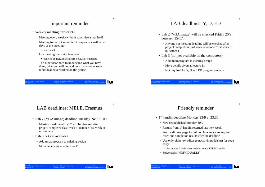
Handin hints
● Common problems previous year– Wrong file name (note .vhdl at end)
● Will if necessary test these after 4 th set has been completed.
– Wrong data types or wrong names● Bit is not std_logic
– Sensitivity list missing signals– Use VHDL version 1993 (vcom -93 INL1_KA.vhdl)– Do NOT use hdl-designer (shown in header!), may also
result in wrong VHDL version being used!– See handin webpage for info on how to access my test
cases and simulation results after the deadlineTSTE12 Design of Digital Systems Department of Electrical Engineering [email protected] Palmkvist Linköping University http://www.isy.liu.se/edu/kurs/TSTE12
10
Control units
● Hard wired– Moore (output only dependent on state)– Mealy (output dependent on state and input)– Fast– Custom designed
● Microcoded– Cheap– Standardized (easy to reuse)
TSTE12 Design of Digital Systems Department of Electrical Engineering [email protected] Palmkvist Linköping University http://www.isy.liu.se/edu/kurs/TSTE12
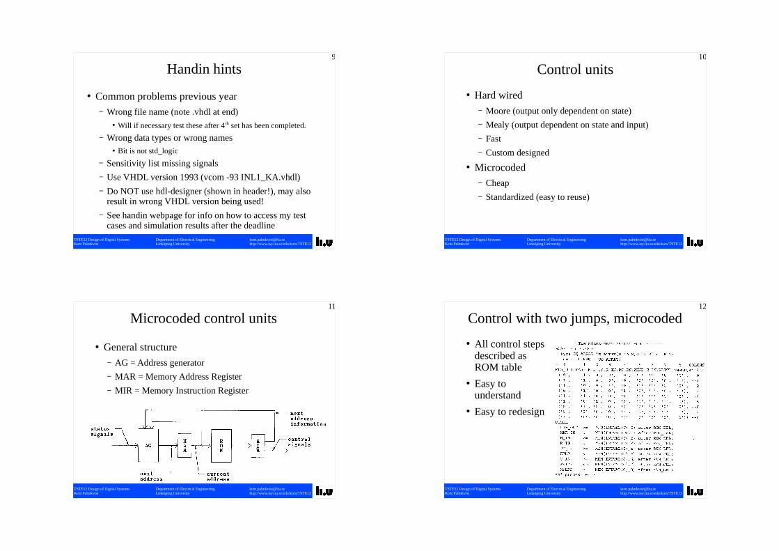
11
● General structure– AG = Address generator– MAR = Memory Address Register– MIR = Memory Instruction Register
Microcoded control units
TSTE12 Design of Digital Systems Department of Electrical Engineering [email protected] Palmkvist Linköping University http://www.isy.liu.se/edu/kurs/TSTE12
12
Control with two jumps, microcoded
● All control steps described asROM table
● Easy to understand
● Easy to redesign
TSTE12 Design of Digital Systems Department of Electrical Engineering [email protected] Palmkvist Linköping University http://www.isy.liu.se/edu/kurs/TSTE12
13
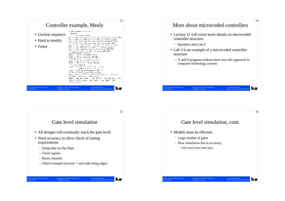
Controller example, Mealy
● Unclear sequence● Hard to modify● Faster
TSTE12 Design of Digital Systems Department of Electrical Engineering [email protected] Palmkvist Linköping University http://www.isy.liu.se/edu/kurs/TSTE12
14
More about microcoded controllers
● Lecture 11 will cover more details on microcoded controller structure– Introduce also Lab 3
● Lab 3 is an example of a microcoded controller structure– Y and D program students have seen this approach in
computer technology courses
TSTE12 Design of Digital Systems Department of Electrical Engineering [email protected] Palmkvist Linköping University http://www.isy.liu.se/edu/kurs/TSTE12
15
Gate level simulation
● All designs will eventually reach the gate level● Need accuracy to allow check of timing
requirements– Setup time on flip-flops– Clock signals– Races, hazards– Glitch example (inverter + and with rising edge)
TSTE12 Design of Digital Systems Department of Electrical Engineering [email protected] Palmkvist Linköping University http://www.isy.liu.se/edu/kurs/TSTE12
16
● Models must be efficient– Large number of gates– Slow simulation due to accuracy
● Still much faster than spice
Gate level simulation, cont.
TSTE12 Design of Digital Systems Department of Electrical Engineering [email protected] Palmkvist Linköping University http://www.isy.liu.se/edu/kurs/TSTE12
17
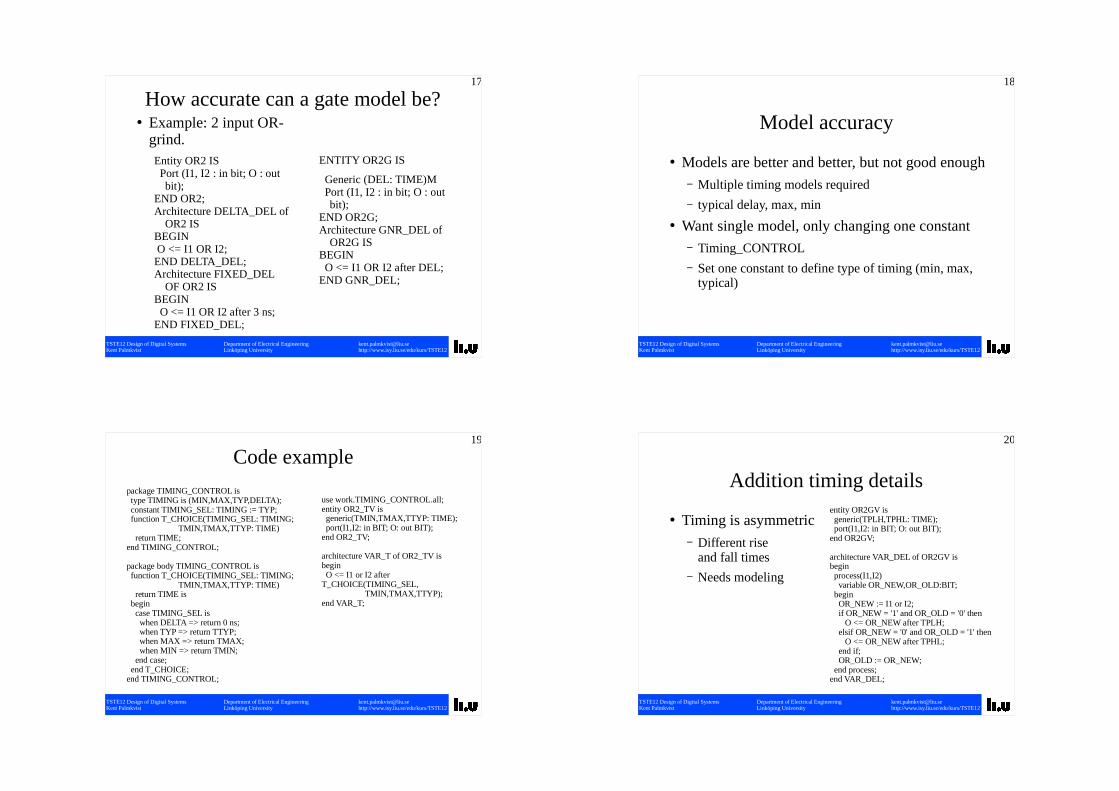
How accurate can a gate model be?● Example: 2 input OR-
grind.Entity OR2 IS Port (I1, I2 : in bit; O : out
bit);END OR2;Architecture DELTA_DEL of
OR2 ISBEGIN O <= I1 OR I2;END DELTA_DEL;Architecture FIXED_DEL
OF OR2 ISBEGIN O <= I1 OR I2 after 3 ns;END FIXED_DEL;
ENTITY OR2G IS
Generic (DEL: TIME)M Port (I1, I2 : in bit; O : out
bit);END OR2G;Architecture GNR_DEL of
OR2G IS BEGIN O <= I1 OR I2 after DEL;END GNR_DEL;
TSTE12 Design of Digital Systems Department of Electrical Engineering [email protected] Palmkvist Linköping University http://www.isy.liu.se/edu/kurs/TSTE12
18
Model accuracy
● Models are better and better, but not good enough– Multiple timing models required– typical delay, max, min
● Want single model, only changing one constant– Timing_CONTROL – Set one constant to define type of timing (min, max,
typical)
TSTE12 Design of Digital Systems Department of Electrical Engineering [email protected] Palmkvist Linköping University http://www.isy.liu.se/edu/kurs/TSTE12
19
Code example
package TIMING_CONTROL is type TIMING is (MIN,MAX,TYP,DELTA); constant TIMING_SEL: TIMING := TYP; function T_CHOICE(TIMING_SEL: TIMING; TMIN,TMAX,TTYP: TIME) return TIME;end TIMING_CONTROL;
package body TIMING_CONTROL is function T_CHOICE(TIMING_SEL: TIMING; TMIN,TMAX,TTYP: TIME) return TIME is begin case TIMING_SEL is when DELTA => return 0 ns; when TYP => return TTYP; when MAX => return TMAX; when MIN => return TMIN; end case; end T_CHOICE;end TIMING_CONTROL;
use work.TIMING_CONTROL.all;entity OR2_TV is generic(TMIN,TMAX,TTYP: TIME); port(I1,I2: in BIT; O: out BIT);end OR2_TV;
architecture VAR_T of OR2_TV isbegin O <= I1 or I2 after T_CHOICE(TIMING_SEL, TMIN,TMAX,TTYP);end VAR_T;
TSTE12 Design of Digital Systems Department of Electrical Engineering [email protected] Palmkvist Linköping University http://www.isy.liu.se/edu/kurs/TSTE12
20
Addition timing details
● Timing is asymmetric– Different rise
and fall times– Needs modeling
entity OR2GV is generic(TPLH,TPHL: TIME); port(I1,I2: in BIT; O: out BIT);end OR2GV;
architecture VAR_DEL of OR2GV isbegin process(I1,I2) variable OR_NEW,OR_OLD:BIT; begin OR_NEW := I1 or I2; if OR_NEW = '1' and OR_OLD = '0' then O <= OR_NEW after TPLH; elsif OR_NEW = '0' and OR_OLD = '1' then O <= OR_NEW after TPHL; end if; OR_OLD := OR_NEW; end process;end VAR_DEL;
TSTE12 Design of Digital Systems Department of Electrical Engineering [email protected] Palmkvist Linköping University http://www.isy.liu.se/edu/kurs/TSTE12
21
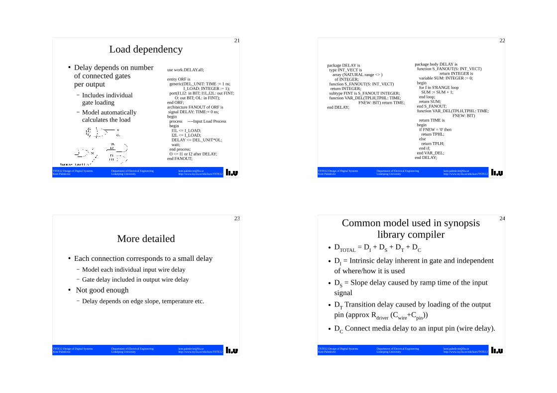
Load dependency
● Delay depends on numberof connected gatesper output– Includes individual
gate loading– Model automatically
calculates the load
use work.DELAY.all;
entity ORF is generic(DEL_UNIT: TIME := 1 ns; I_LOAD: INTEGER := 1); port(I1,I2: in BIT; I1L,I2L: out FINT; O: out BIT; OL: in FINT);end ORF;architecture FANOUT of ORF is signal DELAY: TIME:= 0 ns;begin process ----Input Load Process begin I1L <= I_LOAD; I2L <= I_LOAD; DELAY <= DEL_UNIT*OL; wait; end process; O <= I1 or I2 after DELAY;end FANOUT;
TSTE12 Design of Digital Systems Department of Electrical Engineering [email protected] Palmkvist Linköping University http://www.isy.liu.se/edu/kurs/TSTE12
22
package DELAY is type INT_VECT is array (NATURAL range <> ) of INTEGER; function S_FANOUT(S: INT_VECT) return INTEGER; subtype FINT is S_FANOUT INTEGER; function VAR_DEL(TPLH,TPHL: TIME; FNEW: BIT) return TIME;end DELAY;
package body DELAY is function S_FANOUT(S: INT_VECT) return INTEGER is variable SUM: INTEGER := 0; begin for I in S'RANGE loop SUM := SUM + 1; end loop; return SUM; end S_FANOUT; function VAR_DEL(TPLH,TPHL: TIME; FNEW: BIT) return TIME is begin if FNEW = '0' then return TPHL; else return TPLH; end if; end VAR_DEL;end DELAY;
TSTE12 Design of Digital Systems Department of Electrical Engineering [email protected] Palmkvist Linköping University http://www.isy.liu.se/edu/kurs/TSTE12
23
● Each connection corresponds to a small delay– Model each individual input wire delay– Gate delay included in output wire delay
● Not good enough– Delay depends on edge slope, temperature etc.
More detailed
TSTE12 Design of Digital Systems Department of Electrical Engineering [email protected] Palmkvist Linköping University http://www.isy.liu.se/edu/kurs/TSTE12
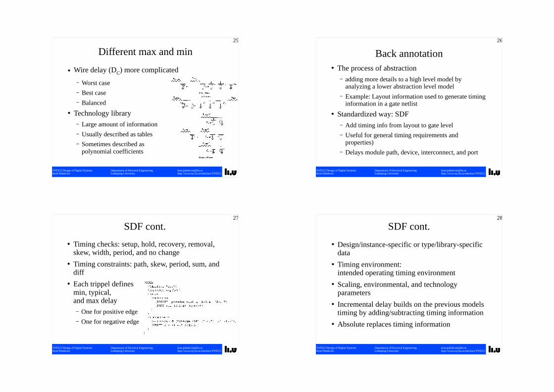
24Common model used in synopsis
library compiler● DTOTAL = DI + DS + DT + DC
● DI = Intrinsic delay inherent in gate and independent of where/how it is used
● DS = Slope delay caused by ramp time of the input signal
● DT Transition delay caused by loading of the output pin (approx Rdriver (Cwire+Cpin))
● DC Connect media delay to an input pin (wire delay).
TSTE12 Design of Digital Systems Department of Electrical Engineering [email protected] Palmkvist Linköping University http://www.isy.liu.se/edu/kurs/TSTE12
25
Different max and min
● Wire delay (DC) more complicated
– Worst case– Best case– Balanced
● Technology library– Large amount of information– Usually described as tables– Sometimes described as
polynomial coefficients
TSTE12 Design of Digital Systems Department of Electrical Engineering [email protected] Palmkvist Linköping University http://www.isy.liu.se/edu/kurs/TSTE12
26
Back annotation● The process of abstraction
– adding more details to a high level model by analyzing a lower abstraction level model
– Example: Layout information used to generate timing information in a gate netlist
● Standardized way: SDF– Add timing info from layout to gate level– Useful for general timing requirements and
properties)– Delays module path, device, interconnect, and port
TSTE12 Design of Digital Systems Department of Electrical Engineering [email protected] Palmkvist Linköping University http://www.isy.liu.se/edu/kurs/TSTE12
27
SDF cont.
● Timing checks: setup, hold, recovery, removal, skew, width, period, and no change
● Timing constraints: path, skew, period, sum, and diff
● Each trippel definesmin, typical, and max delay– One for positive edge– One for negative edge
TSTE12 Design of Digital Systems Department of Electrical Engineering [email protected] Palmkvist Linköping University http://www.isy.liu.se/edu/kurs/TSTE12
28
SDF cont.
● Design/instance-specific or type/library-specific data
● Timing environment: intended operating timing environment
● Scaling, environmental, and technology parameters
● Incremental delay builds on the previous models timing by adding/subtracting timing information
● Absolute replaces timing information
TSTE12 Design of Digital Systems Department of Electrical Engineering [email protected] Palmkvist Linköping University http://www.isy.liu.se/edu/kurs/TSTE12
29
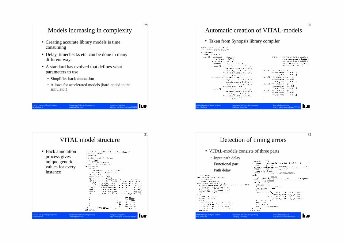
Models increasing in complexity
● Creating accurate library models is time consuming
● Delay, timechecks etc. can be done in many different ways
● A standard has evolved that defines what parameters to use– Simplifies back annotation– Allows for accelerated models (hard-coded in the
simulator)
TSTE12 Design of Digital Systems Department of Electrical Engineering [email protected] Palmkvist Linköping University http://www.isy.liu.se/edu/kurs/TSTE12
30
Automatic creation of VITAL-models
● Taken from Synopsis library compiler
TSTE12 Design of Digital Systems Department of Electrical Engineering [email protected] Palmkvist Linköping University http://www.isy.liu.se/edu/kurs/TSTE12
31
VITAL model structure
● Back annotationprocess givesunique genericvalues for everyinstance
TSTE12 Design of Digital Systems Department of Electrical Engineering [email protected] Palmkvist Linköping University http://www.isy.liu.se/edu/kurs/TSTE12
32
Detection of timing errors
● VITAL-models consists of three parts– Input path delay– Functional part– Path delay
TSTE12 Design of Digital Systems Department of Electrical Engineering [email protected] Palmkvist Linköping University http://www.isy.liu.se/edu/kurs/TSTE12
33
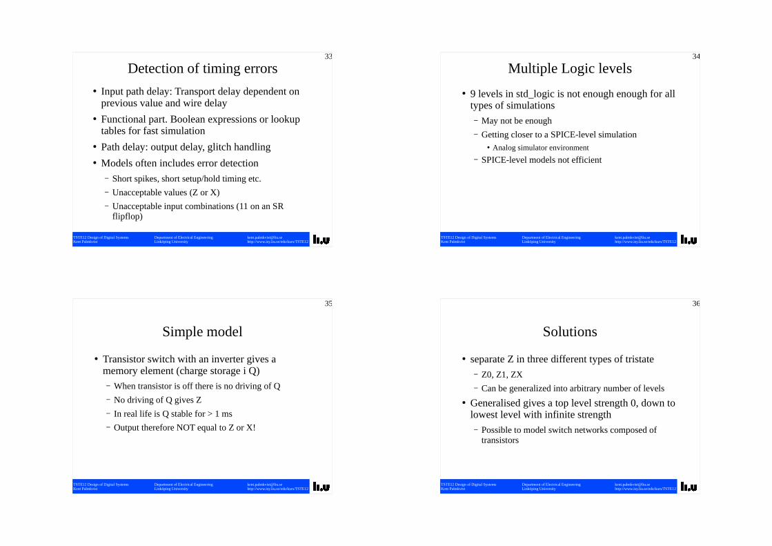
● Input path delay: Transport delay dependent on previous value and wire delay
● Functional part. Boolean expressions or lookup tables for fast simulation
● Path delay: output delay, glitch handling● Models often includes error detection
– Short spikes, short setup/hold timing etc.– Unacceptable values (Z or X)– Unacceptable input combinations (11 on an SR
flipflop)
Detection of timing errors
TSTE12 Design of Digital Systems Department of Electrical Engineering [email protected] Palmkvist Linköping University http://www.isy.liu.se/edu/kurs/TSTE12
34
Multiple Logic levels
● 9 levels in std_logic is not enough enough for all types of simulations– May not be enough– Getting closer to a SPICE-level simulation
● Analog simulator environment
– SPICE-level models not efficient
TSTE12 Design of Digital Systems Department of Electrical Engineering [email protected] Palmkvist Linköping University http://www.isy.liu.se/edu/kurs/TSTE12
35
Simple model
● Transistor switch with an inverter gives a memory element (charge storage i Q)– When transistor is off there is no driving of Q– No driving of Q gives Z– In real life is Q stable for > 1 ms– Output therefore NOT equal to Z or X!
TSTE12 Design of Digital Systems Department of Electrical Engineering [email protected] Palmkvist Linköping University http://www.isy.liu.se/edu/kurs/TSTE12
36
Solutions
● separate Z in three different types of tristate– Z0, Z1, ZX– Can be generalized into arbitrary number of levels
● Generalised gives a top level strength 0, down to lowest level with infinite strength– Possible to model switch networks composed of
transistors
TSTE12 Design of Digital Systems Department of Electrical Engineering [email protected] Palmkvist Linköping University http://www.isy.liu.se/edu/kurs/TSTE12
37
Transistor Model
● Describe value as well as how week driving strength
● Algorithm transistor– If transistor turns off use infinite weakness– If transistor turns on give drain and source strength of
each other decremented by 1– If gate is X give X on source and drain with strength
reduced by 1
TSTE12 Design of Digital Systems Department of Electrical Engineering [email protected] Palmkvist Linköping University http://www.isy.liu.se/edu/kurs/TSTE12
38
Interconnection model
● Algorithm– Find the largest value of all inputs– If the new value is stronger than the old are all the
inputs with lower strength set to the new value– Closer to the SPICE model (execution time?)– Similar to other switch level simulations (e.g. Lsim)
TSTE12 Design of Digital Systems Department of Electrical Engineering [email protected] Palmkvist Linköping University http://www.isy.liu.se/edu/kurs/TSTE12
39
Other ways: Interval logic
● Vantage systems (46 levels)● Example of where it is useful
– Two tristate gates– Both inputs 0– One enable X, other 1– Std_logic gives X (expect 0)– Vantage gives correct value (FZX and F0 => 0)
TSTE12 Design of Digital Systems Department of Electrical Engineering [email protected] Palmkvist Linköping University http://www.isy.liu.se/edu/kurs/TSTE12
40
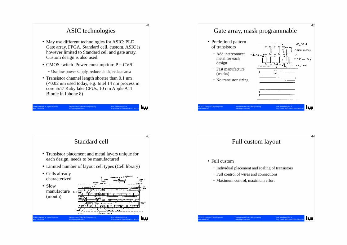
Hardware overview
● Detailed description of Hardware● Standard parts
– TTL (SSI, MSI LSI)– Memories, microprocessors, I/O
● ASIC (Application Specific Integrated Circuit)– Integrated circuit that has been produced for a specific
application and (often) produced in small numbers– Memories and microprocessors are general
application devices
TSTE12 Design of Digital Systems Department of Electrical Engineering [email protected] Palmkvist Linköping University http://www.isy.liu.se/edu/kurs/TSTE12
41
ASIC technologies
● May use different technologies for ASIC: PLD, Gate array, FPGA, Standard cell, custom. ASIC is however limited to Standard cell and gate array. Custom design is also used.
● CMOS switch. Power consumption: P = CV2f– Use low power supply, reduce clock, reduce area
● Transistor channel length shorter than 0.1 um (<0.02 um used today, e.g. Intel 14 nm process in core i5/i7 Kaby lake CPUs, 10 nm Apple A11 Bionic in Iphone 8)
TSTE12 Design of Digital Systems Department of Electrical Engineering [email protected] Palmkvist Linköping University http://www.isy.liu.se/edu/kurs/TSTE12
42
Gate array, mask programmable
● Predefined patternof transistors– Add interconnect
metal for each design
– Fast manufacture(weeks)
– No transistor sizing
TSTE12 Design of Digital Systems Department of Electrical Engineering [email protected] Palmkvist Linköping University http://www.isy.liu.se/edu/kurs/TSTE12
43
Standard cell
● Transistor placement and metal layers unique for each design, needs to be manufactured
● Limited number of layout cell types (Cell library)● Cells already
characterized● Slow
manufacture(month)
TSTE12 Design of Digital Systems Department of Electrical Engineering [email protected] Palmkvist Linköping University http://www.isy.liu.se/edu/kurs/TSTE12
44
Full custom layout
● Full custom– Individual placement and scaling of transistors– Full control of wires and connections– Maximum control, maximum effort
TSTE12 Design of Digital Systems Department of Electrical Engineering [email protected] Palmkvist Linköping University http://www.isy.liu.se/edu/kurs/TSTE12
45
Full custom layout
● Complete freedom to place and route transistors– Not limited to existing logic style/library– Slow manufacture (months)– Higher performance than standard cells
● Requires more testing (simulation)
TSTE12 Design of Digital Systems Department of Electrical Engineering [email protected] Palmkvist Linköping University http://www.isy.liu.se/edu/kurs/TSTE12
46
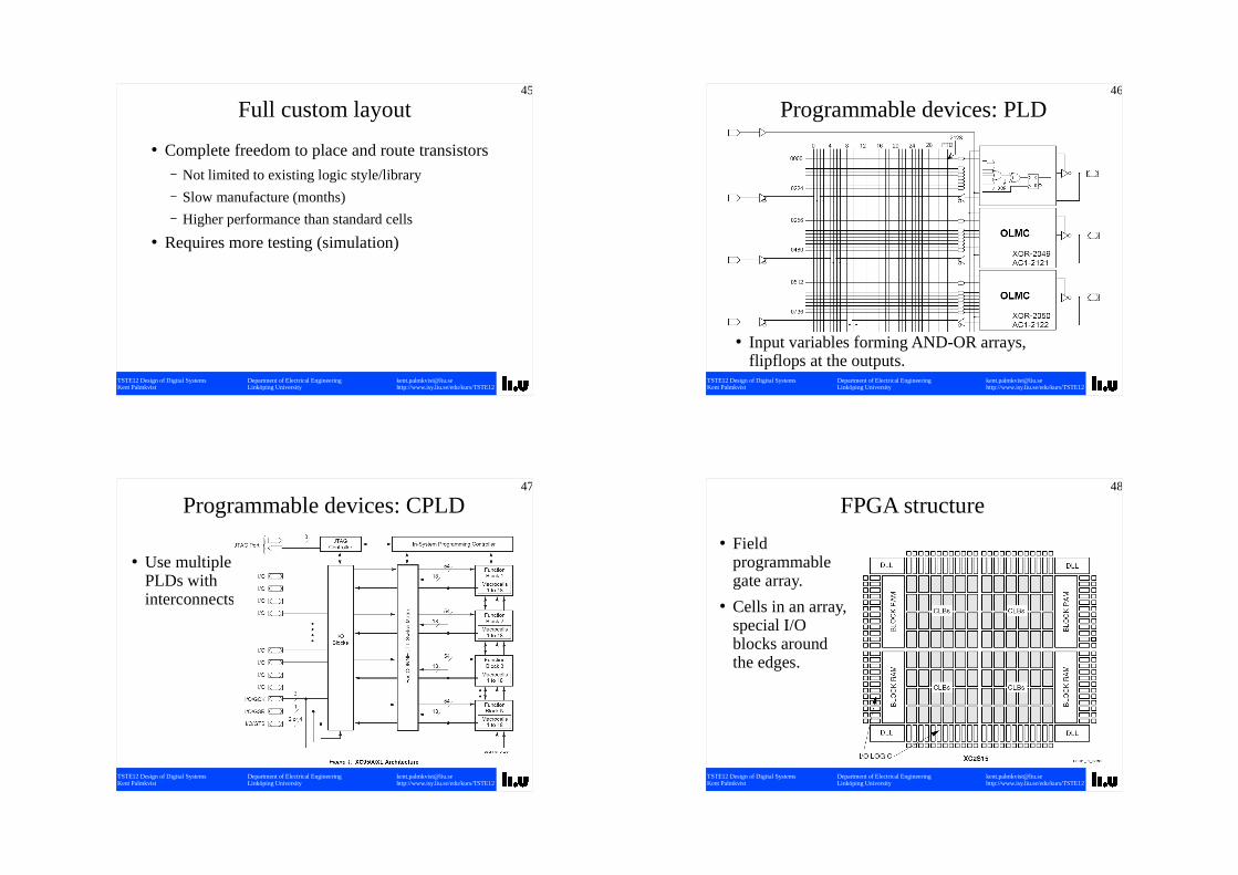
Programmable devices: PLD
● Input variables forming AND-OR arrays, flipflops at the outputs.
TSTE12 Design of Digital Systems Department of Electrical Engineering [email protected] Palmkvist Linköping University http://www.isy.liu.se/edu/kurs/TSTE12
47
Programmable devices: CPLD
● Use multiple PLDs with interconnects
TSTE12 Design of Digital Systems Department of Electrical Engineering [email protected] Palmkvist Linköping University http://www.isy.liu.se/edu/kurs/TSTE12
48
FPGA structure
● Field programmable gate array.
● Cells in an array, special I/O blocks around the edges.
TSTE12 Design of Digital Systems Department of Electrical Engineering [email protected] Palmkvist Linköping University http://www.isy.liu.se/edu/kurs/TSTE12
49
FPGA building blocks
● CLB/Slice– In many cases are they based on lookup tables (i.e.,
no simple gates, instead more advanced functions) => less need for routing channels (that are expensive). Lookup table can be viewed as a small RAM or a MUX with fixed inputs.
– Trade off between big lookup tables and utilization. Optimal around 3-4 bits address.
– Often a flip-flop included in the CLB
TSTE12 Design of Digital Systems Department of Electrical Engineering [email protected] Palmkvist Linköping University http://www.isy.liu.se/edu/kurs/TSTE12
50
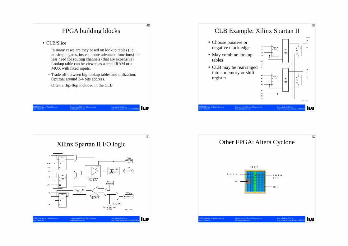
CLB Example: Xilinx Spartan II
● Choose positive or negative clock edge
● May combine lookup tables
● CLB may be rearranged into a memory or shift register
TSTE12 Design of Digital Systems Department of Electrical Engineering [email protected] Palmkvist Linköping University http://www.isy.liu.se/edu/kurs/TSTE12
51
Xilinx Spartan II I/O logic
TSTE12 Design of Digital Systems Department of Electrical Engineering [email protected] Palmkvist Linköping University http://www.isy.liu.se/edu/kurs/TSTE12
52
Other FPGA: Altera Cyclone
E P 1 C 3
P L L
M 4 K R A M B l o c k
L o g i c A r r a y
I O E s
TSTE12 Design of Digital Systems Department of Electrical Engineering [email protected] Palmkvist Linköping University http://www.isy.liu.se/edu/kurs/TSTE12
53
Other FPGA: Altera Cyclone● Logic element structure
TSTE12 Design of Digital Systems Department of Electrical Engineering [email protected] Palmkvist Linköping University http://www.isy.liu.se/edu/kurs/TSTE12
54
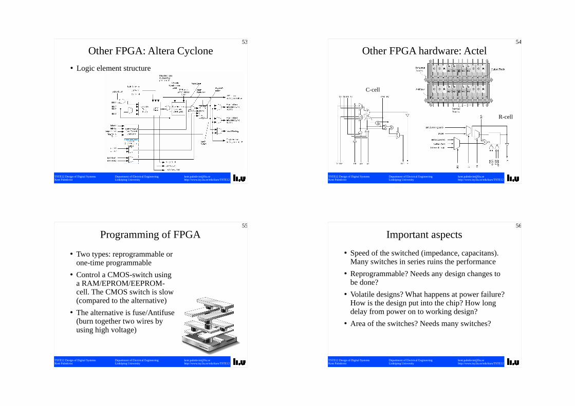
Other FPGA hardware: Actel
C-cell
R-cell
TSTE12 Design of Digital Systems Department of Electrical Engineering [email protected] Palmkvist Linköping University http://www.isy.liu.se/edu/kurs/TSTE12
55
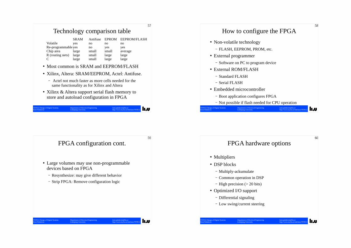
● Two types: reprogrammable or one-time programmable
● Control a CMOS-switch using a RAM/EPROM/EEPROM-cell. The CMOS switch is slow (compared to the alternative)
● The alternative is fuse/Antifuse (burn together two wires by using high voltage)
Programming of FPGA
TSTE12 Design of Digital Systems Department of Electrical Engineering [email protected] Palmkvist Linköping University http://www.isy.liu.se/edu/kurs/TSTE12
56
Important aspects
● Speed of the switched (impedance, capacitans). Many switches in series ruins the performance
● Reprogrammable? Needs any design changes to be done?
● Volatile designs? What happens at power failure? How is the design put into the chip? How long delay from power on to working design?
● Area of the switches? Needs many switches?
TSTE12 Design of Digital Systems Department of Electrical Engineering [email protected] Palmkvist Linköping University http://www.isy.liu.se/edu/kurs/TSTE12
57
Technology comparison table
● Most common is SRAM and EEPROM/FLASH● Xilinx, Altera: SRAM/EEPROM, Actel: Antifuse.
– Actel not much faster as more cells needed for the same functionality as for Xilinx and Altera
● Xilinx & Altera support serial flash memory to store and autoload configuration in FPGA
SRAM Antifuse EPROM EEPROM/FLASHVolatile yes no no noRe-programmableyes no yes yesChip area large small small averageR (routing nets) large small large largeC large small large large
TSTE12 Design of Digital Systems Department of Electrical Engineering [email protected] Palmkvist Linköping University http://www.isy.liu.se/edu/kurs/TSTE12
58
How to configure the FPGA
● Non-volatile technology– FLASH, EEPROM, PROM, etc.
● External programmer– Software on PC to program device
● External ROM/FLASH– Standard FLASH– Serial FLASH
● Embedded microcontroller– Boot application configures FPGA– Not possible if flash needed for CPU operation
TSTE12 Design of Digital Systems Department of Electrical Engineering [email protected] Palmkvist Linköping University http://www.isy.liu.se/edu/kurs/TSTE12
59
FPGA configuration cont.
● Large volumes may use non-programmable devices based on FPGA– Resynthesize: may give different behavior– Strip FPGA: Remove configuration logic
TSTE12 Design of Digital Systems Department of Electrical Engineering [email protected] Palmkvist Linköping University http://www.isy.liu.se/edu/kurs/TSTE12
60
FPGA hardware options
● Multipliers● DSP blocks
– Multiply-ackumulate– Common operation in DSP– High precision (> 20 bits)
● Optimized I/O support– Differential signaling– Low swing/current steering
TSTE12 Design of Digital Systems Department of Electrical Engineering [email protected] Palmkvist Linköping University http://www.isy.liu.se/edu/kurs/TSTE12
61
FPGA Hardware options, cont.
● Clock circuits– Phase locked loops (PLL), Delay locked loops (DLL)– Clock tree distribution
● Serializer/deserializer– Support modern PC bus standards such as PCI
Express– Reduce number of I/O pins
TSTE12 Design of Digital Systems Department of Electrical Engineering [email protected] Palmkvist Linköping University http://www.isy.liu.se/edu/kurs/TSTE12
62
FPGA Hardware options, cont.
● A/D and D/A converters● Memory units● CPU
– e.g., physical powerpc or ARM core inside FPGA
TSTE12 Design of Digital Systems Department of Electrical Engineering [email protected] Palmkvist Linköping University http://www.isy.liu.se/edu/kurs/TSTE12
63
ASIC vs FPGA
● ASIC have a large NRE cost– Non-recurring engineering cost, price of 1 st unit
● FPGA have large per unit cost● Selection of technology depend on
– Performance requirements– Number of units– Time to market