Embed Size (px)
Citation preview
8-1 Chapter 8—Input and Output
Computer Systems Design and Architecture by V. Heuring and H. Jordan © 1997 V. Heuring and H. Jordan
Chapter 8: Input and Output
8.1 The I/O Subsystem• I/O buses and addresses
8.2 Programmed I/O• I/O operations initiated by program instructions
8.3 I/O Interrupts• Requests to processor for service from an I/O device
8.4 Direct Memory Access (DMA)• Moving data in and out without processor intervention
8.5 I/O Data Format Change and Error Control• Error detection and correction coding of I/O data
Topics
8-2 Chapter 8—Input and Output
Computer Systems Design and Architecture by V. Heuring and H. Jordan © 1997 V. Heuring and H. Jordan
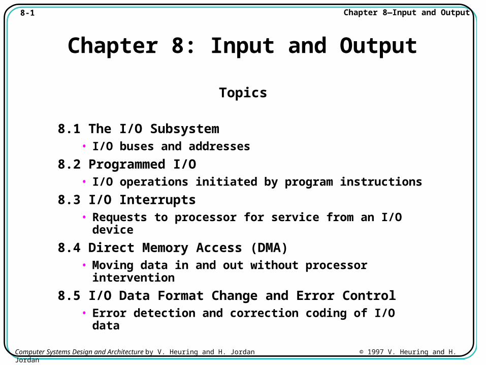
Three Requirements of I/O Data Transmission
(1) Data location• Correct device must be selected
• Data must be addressed within that device
(2) Data transfer• Amount of data varies with device and may need be
specified
• Transmission rate varies greatly with device
• Data may be output, input, or either with a given device
(3) Synchronization• For an output device, data must be sent only when the
device is ready to receive it
• For an input device, the processor can read data only when it is available from the device
8-3 Chapter 8—Input and Output
Computer Systems Design and Architecture by V. Heuring and H. Jordan © 1997 V. Heuring and H. Jordan
Location of I/O Data
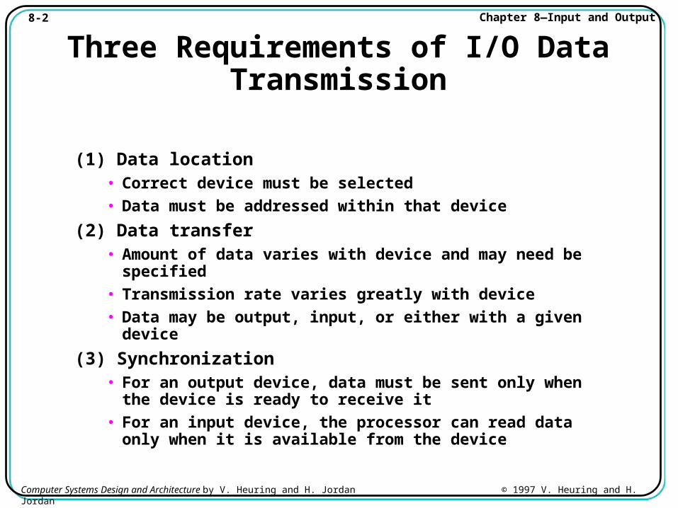
• Data location may be trivial once the device is determined
• Character from a keyboard
• Character out to a serial printer
• Location may involve searching• Record number on a tape drive
• Track seek and rotation to sector on a disk
• Location may not be simple binary number• Drive, platter, track, sector, word on a disk cluster
8-4 Chapter 8—Input and Output
Computer Systems Design and Architecture by V. Heuring and H. Jordan © 1997 V. Heuring and H. Jordan
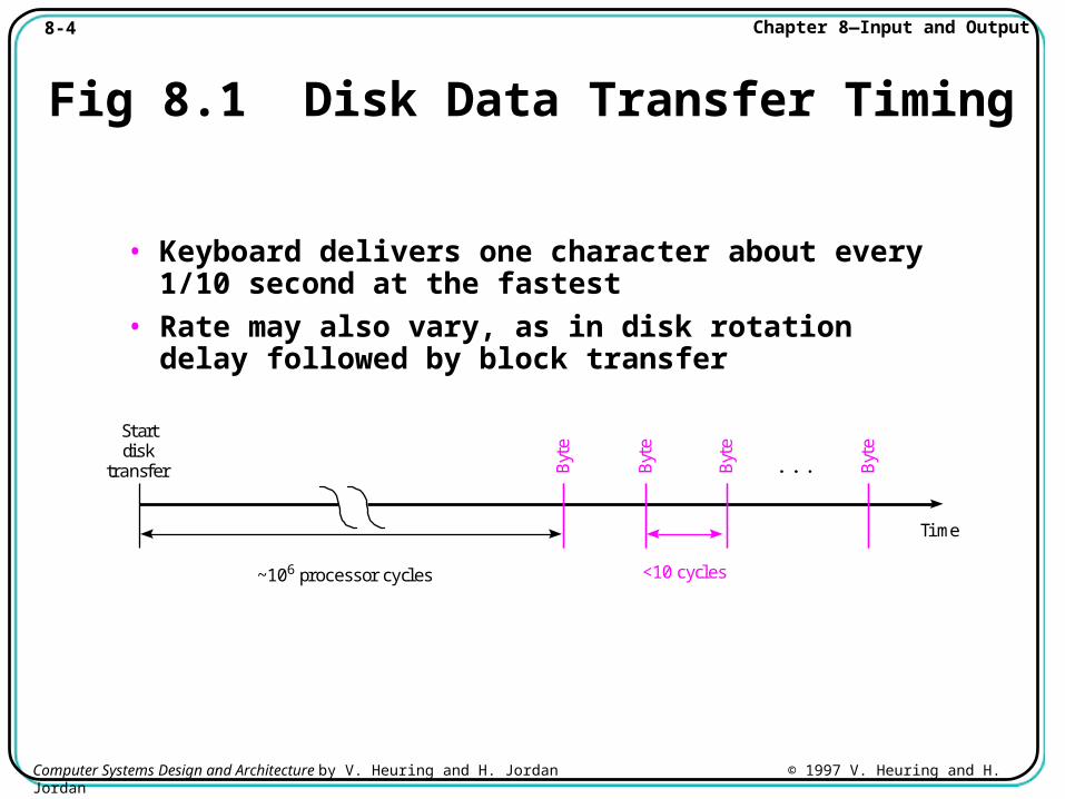
Fig 8.1 Disk Data Transfer Timing
• Keyboard delivers one character about every 1/10 second at the fastest
• Rate may also vary, as in disk rotation delay followed by block transfer
Byt
e
Byt
e
Byt
e
Byt
e
Startdisk
transfer
~106 processor cycles
Time
<10 cycles
8-5 Chapter 8—Input and Output
Computer Systems Design and Architecture by V. Heuring and H. Jordan © 1997 V. Heuring and H. Jordan
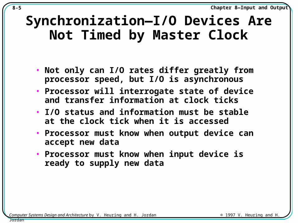
Synchronization—I/O Devices Are Not Timed by Master Clock
• Not only can I/O rates differ greatly from processor speed, but I/O is asynchronous
• Processor will interrogate state of device and transfer information at clock ticks
• I/O status and information must be stable at the clock tick when it is accessed
• Processor must know when output device can accept new data
• Processor must know when input device is ready to supply new data
8-6 Chapter 8—Input and Output
Computer Systems Design and Architecture by V. Heuring and H. Jordan © 1997 V. Heuring and H. Jordan
Reducing Location and Synchronization to Data Transfer
• Since the structure of device data location is device dependent, device should interpret it
• The device must be selected by the processor, but
• Location within the device is just information passed to the device
• Synchronization can be done by the processor reading device status bits
• Data available signal from input device
• Ready to accept output data from output device
• Speed requirements will require us to use other forms of synchronization: discussed later
• Interrupts and DMA are examples
8-7 Chapter 8—Input and Output
Computer Systems Design and Architecture by V. Heuring and H. Jordan © 1997 V. Heuring and H. Jordan
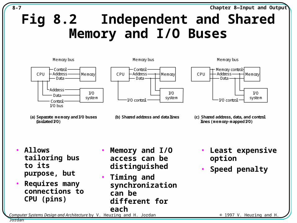
Fig 8.2 Independent and Shared Memory and I/O Buses
• Allows tailoring bus to its purpose, but
• Requires many connections to CPU (pins)
• Least expensive option
• Speed penalty
• Memory and I/O access can be distinguished
• Timing and synchronization can be different for each
Memory bus
ControlAddress
Data
ControlI/O bus
AddressData
(a) Separate memory and I/O buses(isolated I/O)
Memory
I/Osystem
CPU
Memory bus
ControlAddress
Data
I/O control
(b) Shared address and data lines
Memory
I/Osystem
CPU
Memory bus
Memory controlAddress
Data
I/O control
(c) Shared address, data, and controllines (memory-mapped I/O)
Memory
I/Osystem
CPU
8-8 Chapter 8—Input and Output
Computer Systems Design and Architecture by V. Heuring and H. Jordan © 1997 V. Heuring and H. Jordan
Memory-Mapped I/O
• Combine memory control and I/O control lines to make one unified bus for memory and I/O
• This makes addresses of I/O device registers appear to the processor as memory addresses
• Reduces the number of connections to the processor chip
• Increased generality may require a few more control signals
• Standardizes data transfer to and from the processor• Asynchronous operation is optional with memory, but
demanded by I/O devices
8-9 Chapter 8—Input and Output
Computer Systems Design and Architecture by V. Heuring and H. Jordan © 1997 V. Heuring and H. Jordan
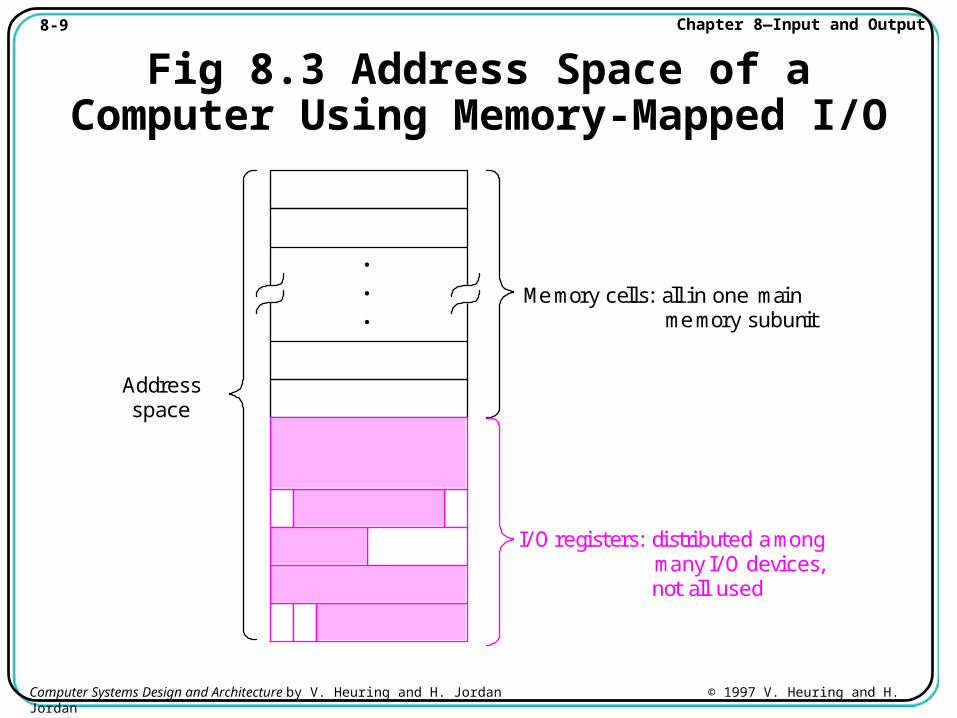
Fig 8.3 Address Space of a Computer Using Memory-Mapped I/O
Addressspace
I/O registers: distributed amongmany I/O devices,not all used
Memory cells: all in one mainmemory subunit
. . .
8-10 Chapter 8—Input and Output
Computer Systems Design and Architecture by V. Heuring and H. Jordan © 1997 V. Heuring and H. Jordan
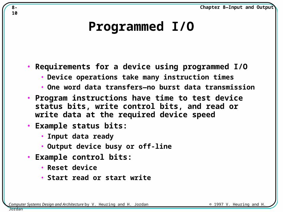
Programmed I/O
• Requirements for a device using programmed I/O• Device operations take many instruction times
• One word data transfers—no burst data transmission
• Program instructions have time to test device status bits, write control bits, and read or write data at the required device speed
• Example status bits:• Input data ready
• Output device busy or off-line
• Example control bits:• Reset device
• Start read or start write
8-11 Chapter 8—Input and Output
Computer Systems Design and Architecture by V. Heuring and H. Jordan © 1997 V. Heuring and H. Jordan
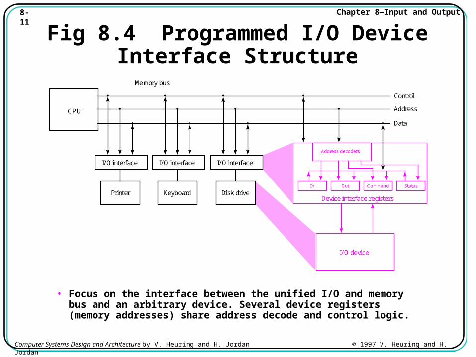
Fig 8.4 Programmed I/O Device Interface Structure
• Focus on the interface between the unified I/O and memory bus and an arbitrary device. Several device registers (memory addresses) share address decode and control logic.
CPU
Memory bus
Data
Address
Control
I/O interface
Printer
I/O interface
Keyboard
I/O interface
Disk drive
I/O device
In Out
Address decoders
Command
Device interface registers
Status
8-12 Chapter 8—Input and Output
Computer Systems Design and Architecture by V. Heuring and H. Jordan © 1997 V. Heuring and H. Jordan
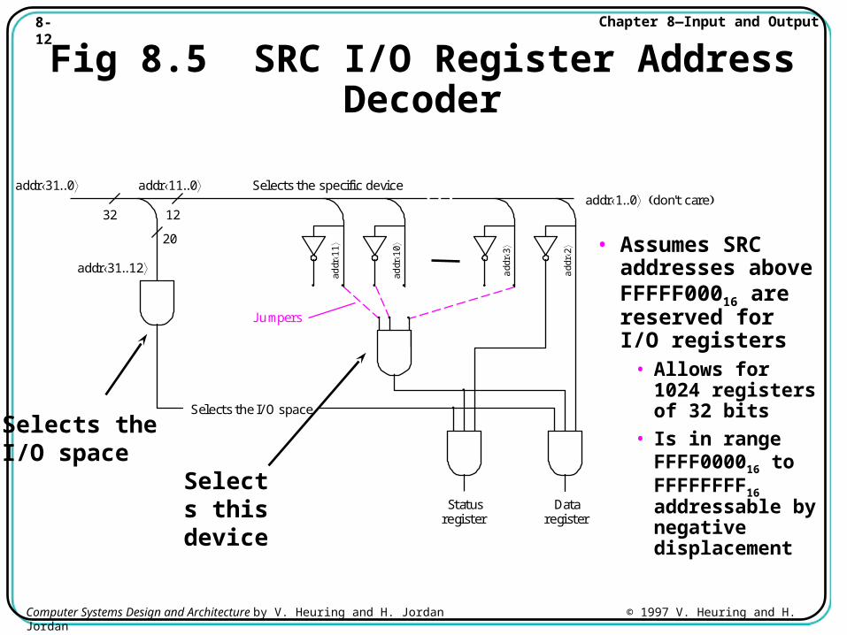
Fig 8.5 SRC I/O Register Address Decoder
• Assumes SRC addresses above FFFFF00016 are reserved for I/O registers
• Allows for 1024 registers of 32 bits
• Is in range FFFF000016 to FFFFFFFF16 addressable by negative displacement
Selects the I/O space
Selects this device
32 12
20
addr31..0
addr31..12
addr11..0addr1..0 don't care
ad
dr
11
Selects the specific device
Jumpers
Selects the I/O space
Statusregister
Dataregister
ad
dr
10
add
r 3
add
r 2
8-13 Chapter 8—Input and Output
Computer Systems Design and Architecture by V. Heuring and H. Jordan © 1997 V. Heuring and H. Jordan
Fig 8.6 Interface Design for SRC Character Output
32
1
8 8 Character
Toprinter
ToCPU
address31..0
data31
(status)
Start
Done
TS
data7..0(character)
Read (status)
Complete
Write (data)
Statusregister
Address decoder
Dataregister
D 1
Ready
CLR
Q
Q
D
Char
Q
Q
TS
TS
2
1
3
4
8-14 Chapter 8—Input and Output
Computer Systems Design and Architecture by V. Heuring and H. Jordan © 1997 V. Heuring and H. Jordan
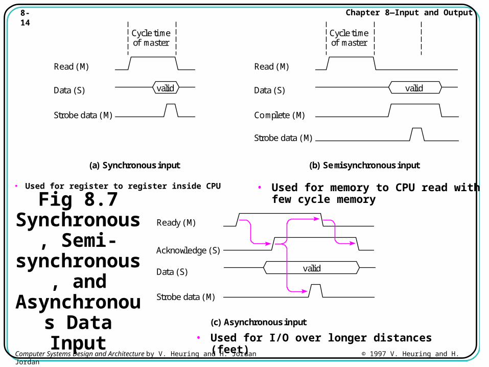
Fig 8.7 Synchronous,
Semi-synchronous,
and Asynchronous
Data Input
• Used for register to register inside CPU • Used for memory to CPU read with few cycle memory
• Used for I/O over longer distances (feet)
Read (M)
Data (S) valid
Cycle timeof master
Strobe data (M)
Ready (M)
Data (S)
Acknowledge (S)
valid
Strobe data (M)
Read (M)
Data (S)
(a) Synchronous input (b) Semisynchronous input
(c) Asynchronous input
valid
Cycle timeof master
Complete (M)
Strobe data (M)
8-15 Chapter 8—Input and Output
Computer Systems Design and Architecture by V. Heuring and H. Jordan © 1997 V. Heuring and H. Jordan
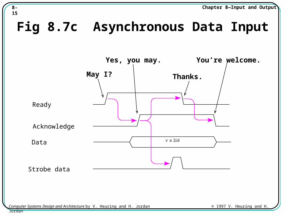
Fig 8.7c Asynchronous Data Input
May I?
Yes, you may.
Thanks.
You’re welcome.
v a l i d
Ready
Acknowledge
Data
Strobe data
8-16 Chapter 8—Input and Output
Computer Systems Design and Architecture by V. Heuring and H. Jordan © 1997 V. Heuring and H. Jordan
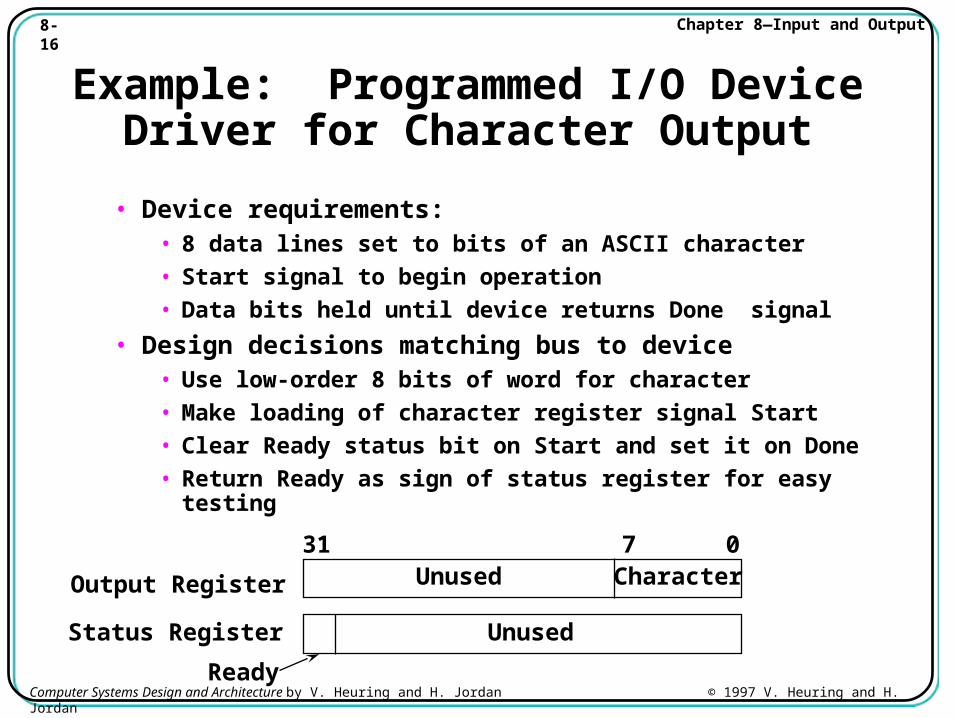
Example: Programmed I/O Device Driver for Character Output
• Device requirements:• 8 data lines set to bits of an ASCII character
• Start signal to begin operation
• Data bits held until device returns Done signal
• Design decisions matching bus to device• Use low-order 8 bits of word for character
• Make loading of character register signal Start
• Clear Ready status bit on Start and set it on Done
• Return Ready as sign of status register for easy testing
Output Register
Status Register
31 07Character
Ready
Unused
Unused
8-17 Chapter 8—Input and Output
Computer Systems Design and Architecture by V. Heuring and H. Jordan © 1997 V. Heuring and H. Jordan
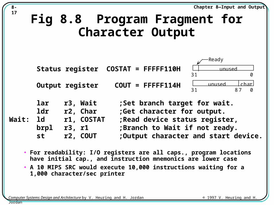
Fig 8.8 Program Fragment for Character Output
• For readability: I/O registers are all caps., program locations have initial cap., and instruction mnemonics are lower case
• A 10 MIPS SRC would execute 10,000 instructions waiting for a 1,000 character/sec printer
Status register COSTAT = FFFFF110H
Output register COUT = FFFFF114H
lar r3, Wait ;Set branch target for wait. ldr r2, Char ;Get character for output.Wait: ld r1, COSTAT ;Read device status register, brpl r3, r1 ;Branch to Wait if not ready. st r2, COUT ;Output character and start device.
31 8 7 0
31 0
Ready
unused
unused char
8-18 Chapter 8—Input and Output
Computer Systems Design and Architecture by V. Heuring and H. Jordan © 1997 V. Heuring and H. Jordan
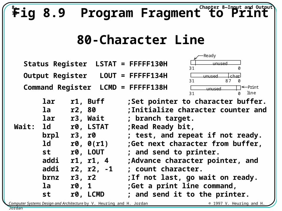
Fig 8.9 Program Fragment to Print 80-Character Line
Status Register LSTAT = FFFFF130H
lar r1, Buff ;Set pointer to character buffer.la r2, 80 ;Initialize character counter andlar r3, Wait ; branch target.
Wait: ld r0, LSTAT ;Read Ready bit,brpl r3, r0 ; test, and repeat if not ready.ld r0, 0(r1) ;Get next character from buffer,st r0, LOUT ; and send to printer.addi r1, r1, 4 ;Advance character pointer, andaddi r2, r2, -1 ; count character.brnz r3, r2 ;If not last, go wait on ready.la r0, 1 ;Get a print line command,st r0, LCMD ; and send it to the printer.
Output Register LOUT = FFFFF134H
Command Register LCMD = FFFFF138H31 8 7 0
31 0
Ready
unused
unused char
31 0unused Pr in t
l i ne
8-19 Chapter 8—Input and Output
Computer Systems Design and Architecture by V. Heuring and H. Jordan © 1997 V. Heuring and H. Jordan
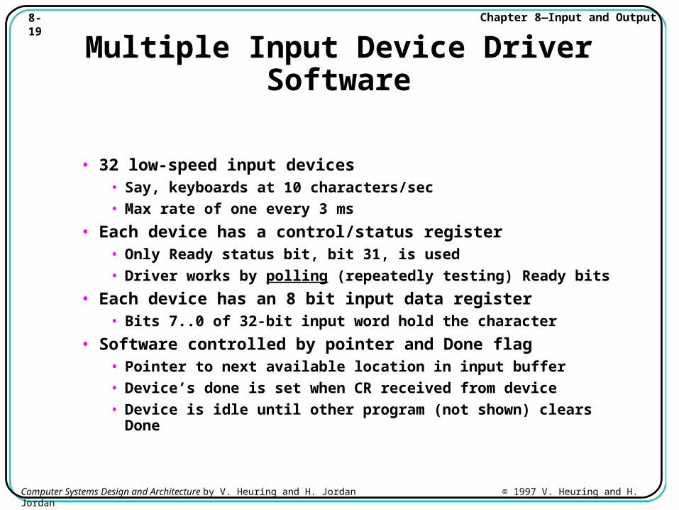
Multiple Input Device Driver Software
• 32 low-speed input devices• Say, keyboards at 10 characters/sec
• Max rate of one every 3 ms
• Each device has a control/status register• Only Ready status bit, bit 31, is used
• Driver works by polling (repeatedly testing) Ready bits
• Each device has an 8 bit input data register• Bits 7..0 of 32-bit input word hold the character
• Software controlled by pointer and Done flag• Pointer to next available location in input buffer
• Device’s done is set when CR received from device
• Device is idle until other program (not shown) clears Done
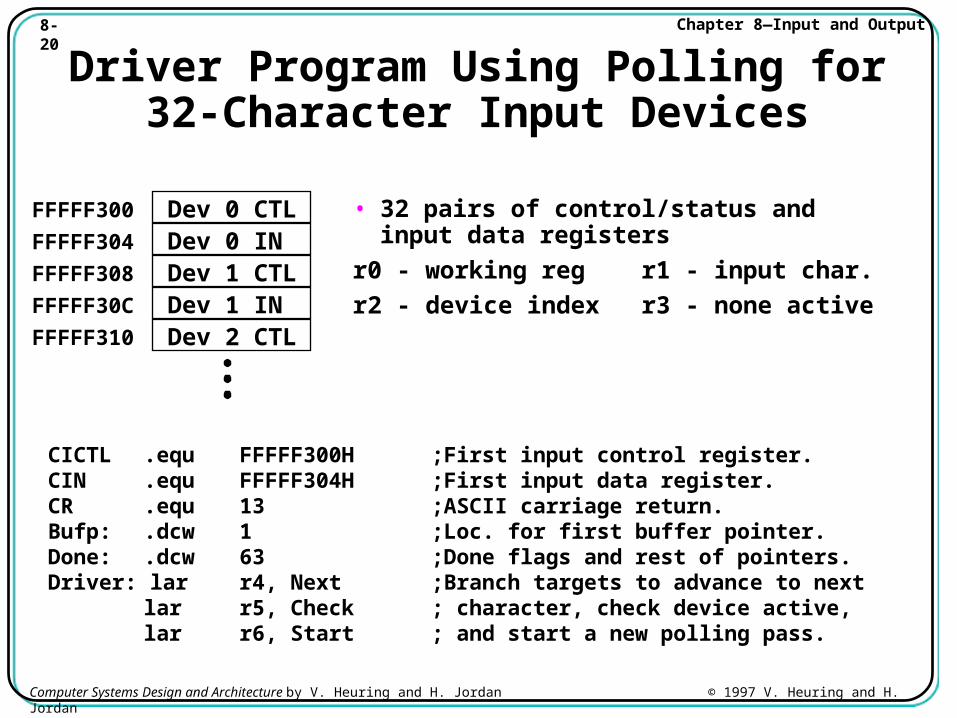
8-20 Chapter 8—Input and Output
Computer Systems Design and Architecture by V. Heuring and H. Jordan © 1997 V. Heuring and H. Jordan
Driver Program Using Polling for 32-Character Input Devices
CICTL .equ FFFFF300H ;First input control register.CIN .equ FFFFF304H ;First input data register.CR .equ 13 ;ASCII carriage return.Bufp: .dcw 1 ;Loc. for first buffer pointer.Done: .dcw 63 ;Done flags and rest of pointers.Driver: lar r4, Next ;Branch targets to advance to next
lar r5, Check ; character, check device active,lar r6, Start ; and start a new polling pass.
• 32 pairs of control/status and input data registers
r0 - working reg r1 - input char.
r2 - device index r3 - none active
Dev 0 CTL
Dev 1 CTL
Dev 2 CTL
Dev 0 IN
Dev 1 IN
FFFFF300
FFFFF304
FFFFF308
FFFFF30C
FFFFF310
8-21 Chapter 8—Input and Output
Computer Systems Design and Architecture by V. Heuring and H. Jordan © 1997 V. Heuring and H. Jordan
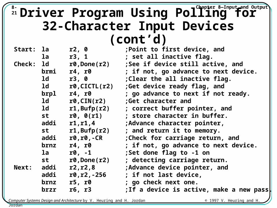
Driver Program Using Polling for 32-Character Input Devices (cont’d)
Start: la r2, 0 ;Point to first device, andla r3, 1 ; set all inactive flag.
Check: ld r0,Done(r2) ;See if device still active, andbrmi r4, r0 ; if not, go advance to next device.ld r3, 0 ;Clear the all inactive flag.ld r0,CICTL(r2) ;Get device ready flag, andbrpl r4, r0 ; go advance to next if not ready.ld r0,CIN(r2) ;Get character andld r1,Bufp(r2) ; correct buffer pointer, andst r0, 0(r1) ; store character in buffer.addi r1,r1,4 ;Advance character pointer,st r1,Bufp(r2) ; and return it to memory.addi r0,r0,-CR ;Check for carriage return, andbrnz r4, r0 ; if not, go advance to next device.la r0, -1 ;Set done flag to -1 onst r0,Done(r2) ; detecting carriage return.
Next: addi r2,r2,8 ;Advance device pointer, andaddi r0,r2,-256 ; if not last device,brnz r5, r0 ; go check next one.brzr r6, r3 ;If a device is active, make a new pass.
8-22 Chapter 8—Input and Output
Computer Systems Design and Architecture by V. Heuring and H. Jordan © 1997 V. Heuring and H. Jordan
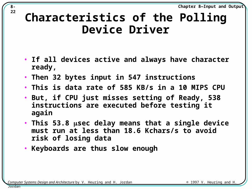
Characteristics of the Polling Device Driver
• If all devices active and always have character ready,
• Then 32 bytes input in 547 instructions
• This is data rate of 585 KB/s in a 10 MIPS CPU
• But, if CPU just misses setting of Ready, 538 instructions are executed before testing it again
• This 53.8 sec delay means that a single device must run at less than 18.6 Kchars/s to avoid risk of losing data
• Keyboards are thus slow enough
8-23 Chapter 8—Input and Output
Computer Systems Design and Architecture by V. Heuring and H. Jordan © 1997 V. Heuring and H. Jordan
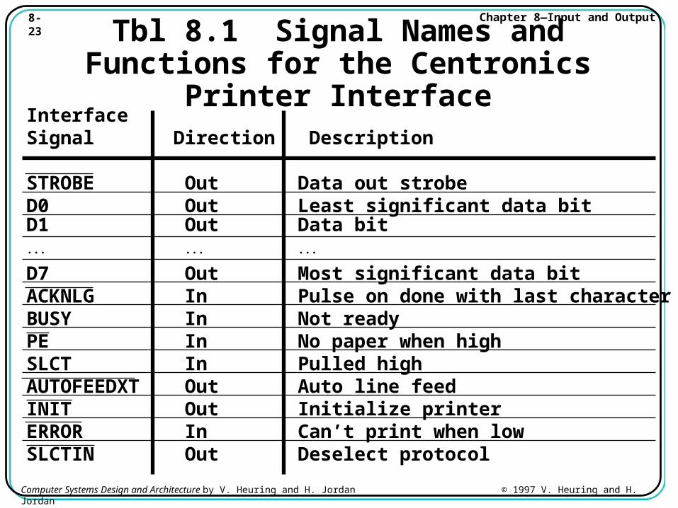
Tbl 8.1 Signal Names and Functions for the Centronics Printer Interface
InterfaceSignal Direction Description
STROBE Out Data out strobeD0 Out Least significant data bitD1 Out Data bit... ... ...D7 Out Most significant data bitACKNLG In Pulse on done with last characterBUSY In Not readyPE In No paper when highSLCT In Pulled highAUTOFEEDXT Out Auto line feedINIT Out Initialize printerERROR In Can’t print when lowSLCTIN Out Deselect protocol
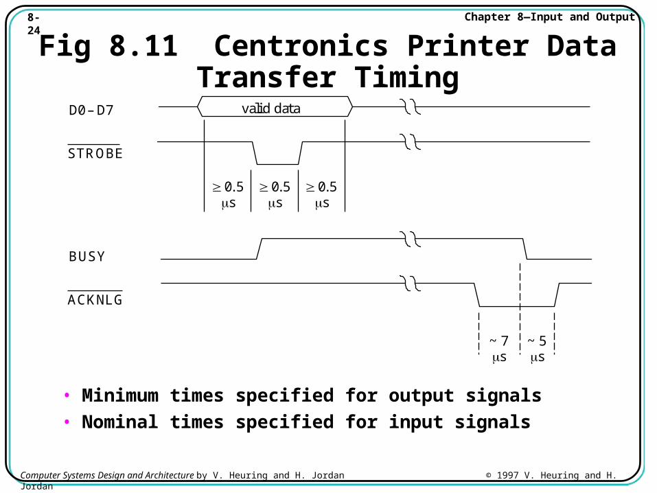
8-24 Chapter 8—Input and Output
Computer Systems Design and Architecture by V. Heuring and H. Jordan © 1997 V. Heuring and H. Jordan
Fig 8.11 Centronics Printer Data Transfer Timing
• Minimum times specified for output signals
• Nominal times specified for input signals
0.5s
0.5s
0.5s
D0–D7 valid data
STROBE
BUSY
ACKNLG
~ 5s
~ 7s
8-25 Chapter 8—Input and Output
Computer Systems Design and Architecture by V. Heuring and H. Jordan © 1997 V. Heuring and H. Jordan
I/O Interrupts
• Key idea: instead of processor executing wait loop, device requests interrupt when ready
• In SRC the interrupting device must return the vector address and interrupt information bits
• Processor must tell device when to send this information—done by acknowledge signal
• Request and acknowledge form a communication handshake pair
• It should be possible to disable interrupts from individual devices
8-26 Chapter 8—Input and Output
Computer Systems Design and Architecture by V. Heuring and H. Jordan © 1997 V. Heuring and H. Jordan
Fig 8.12 Simplified Interrupt Circuit for an I/O Interface
• Request and enable flags per device
• Returns vector and interrupt information on bus when acknowledged
Interruptrequest
Interruptenable
vect7..0
info15..0
data23..16
data15..0
ireq
iack
D Q
Q
D Q
Q
o.c.
8-27 Chapter 8—Input and Output
Computer Systems Design and Architecture by V. Heuring and H. Jordan © 1997 V. Heuring and H. Jordan
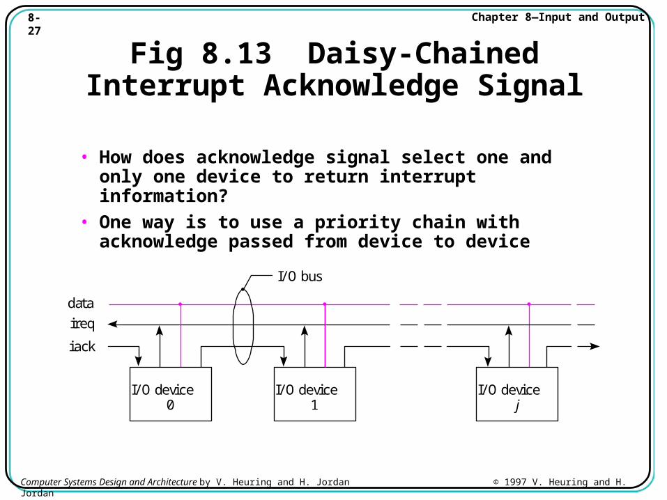
Fig 8.13 Daisy-Chained Interrupt Acknowledge Signal
• How does acknowledge signal select one and only one device to return interrupt information?
• One way is to use a priority chain with acknowledge passed from device to device
I/O bus
data
ireq
iack
I/O device0
I/O device1
I/O devicej
8-28 Chapter 8—Input and Output
Computer Systems Design and Architecture by V. Heuring and H. Jordan © 1997 V. Heuring and H. Jordan
Fig 8.14 Interrupt Logic in an I/O Interface
• Request set by Ready, cleared by acknowledge
• iack only sent out if this device not requesting
RequestReady Enable
ireq
iack(in)
o.c.
TS
TS
TS
TS
TS
Control register address
TS
TS
vect7..0
info15..0
data23..16
data0
Complete
Write
Read1531 2324
Control register
iack data
16 0
31 30Unused
Interrupt requestReady Interrupt enable
infovectUnused
0
data30
data31
data15..0
D Q
Q
D Q
Q
iack (out)
D Q
Q
8-29 Chapter 8—Input and Output
Computer Systems Design and Architecture by V. Heuring and H. Jordan © 1997 V. Heuring and H. Jordan
Getline Subroutine for Interrupt-Driven Character I/O
unused -vect
Ready Int. req. Int. enb.
31 30 0411CICTL
;Getline is called with return address in R31 and a pointer to a;character buffer in R1. It will input characters up to a carriage;return under interrupt control, setting Done to -1 when complete.CR .equ 13 ;ASCII code for carriage return.CIvec .equ 01F0H ;Character input interrupt vector address.Bufp: .dw 1 ;Pointer to next character location.Save: .dw 2 ;Save area for registers on interrupt.Done: .dw 1 ;Flag location is -1 if input complete.Getln: st r1, Bufp ;Record pointer to next character.
edi ;Disable interrupts while changing mask.la r2, 1F1H ;Get vector address and device enable bitst r2, CICTL ; and put into control register of device.la r3, 0 ;Clear thest r3, Done ; line input done flag.een ;Enable Interruptsbr r31 ; and return to caller.
8-30 Chapter 8—Input and Output
Computer Systems Design and Architecture by V. Heuring and H. Jordan © 1997 V. Heuring and H. Jordan
Interrupt Handler for SRC Character Input
.org CIvec ;Start handler at vector address.str r0, Save ;Save the registers thatstr r1, Save+4 ; will be used by the interrupt handler.ldr r1, Bufp ;Get pointer to next character position.ld r0, CIN ;Get the character and enable next input.st r0, 0(r1) ;Store character in line buffer.addi r1, r1, 4 ;Advance pointer andstr r1, Bufp ; store for next interrupt.lar r1, Exit ;Set branch target.addi r0,r0, -CR ;Carriage return? addi with minus CR.brnz r1, r0 ;Exit if not CR, else complete line.la r0, 0 ;Turn off input device byst r0, CICTL ; disabling its interrupts.la r0, -1 ;Get a -1 indicator, andstr r0, Done ; report line input complete.
Exit: ldr r0, Save ;Restore registersldr r1, Save+4 ; of interrupted program.rfi ;Return to interrupted program.
8-31 Chapter 8—Input and Output
Computer Systems Design and Architecture by V. Heuring and H. Jordan © 1997 V. Heuring and H. Jordan
General Functions of an Interrupt Handler
(1) Save the state of the interrupted program
(2) Do programmed I/O operations to satisfy the interrupt request
(3) Restart or turn off the interrupting device
(4) Restore the state and return to the interrupted program
8-32 Chapter 8—Input and Output
Computer Systems Design and Architecture by V. Heuring and H. Jordan © 1997 V. Heuring and H. Jordan
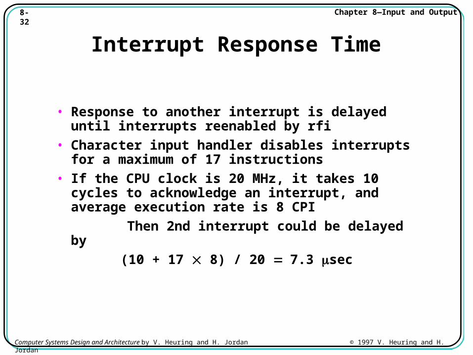
Interrupt Response Time
• Response to another interrupt is delayed until interrupts reenabled by rfi
• Character input handler disables interrupts for a maximum of 17 instructions
• If the CPU clock is 20 MHz, it takes 10 cycles to acknowledge an interrupt, and average execution rate is 8 CPI
Then 2nd interrupt could be delayed by
(10 + 17 8) / 20 7.3 sec
8-33 Chapter 8—Input and Output
Computer Systems Design and Architecture by V. Heuring and H. Jordan © 1997 V. Heuring and H. Jordan
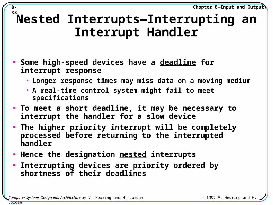
Nested Interrupts—Interrupting an Interrupt Handler
• Some high-speed devices have a deadline for interrupt response• Longer response times may miss data on a moving medium
• A real-time control system might fail to meet specifications
• To meet a short deadline, it may be necessary to interrupt the handler for a slow device
• The higher priority interrupt will be completely processed before returning to the interrupted handler
• Hence the designation nested interrupts
• Interrupting devices are priority ordered by shortness of their deadlines
8-34 Chapter 8—Input and Output
Computer Systems Design and Architecture by V. Heuring and H. Jordan © 1997 V. Heuring and H. Jordan
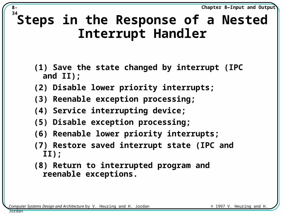
Steps in the Response of a Nested Interrupt Handler
(1) Save the state changed by interrupt (IPC and II);
(2) Disable lower priority interrupts;
(3) Reenable exception processing;
(4) Service interrupting device;
(5) Disable exception processing;
(6) Reenable lower priority interrupts;
(7) Restore saved interrupt state (IPC and II);
(8) Return to interrupted program and reenable exceptions.
8-35 Chapter 8—Input and Output
Computer Systems Design and Architecture by V. Heuring and H. Jordan © 1997 V. Heuring and H. Jordan
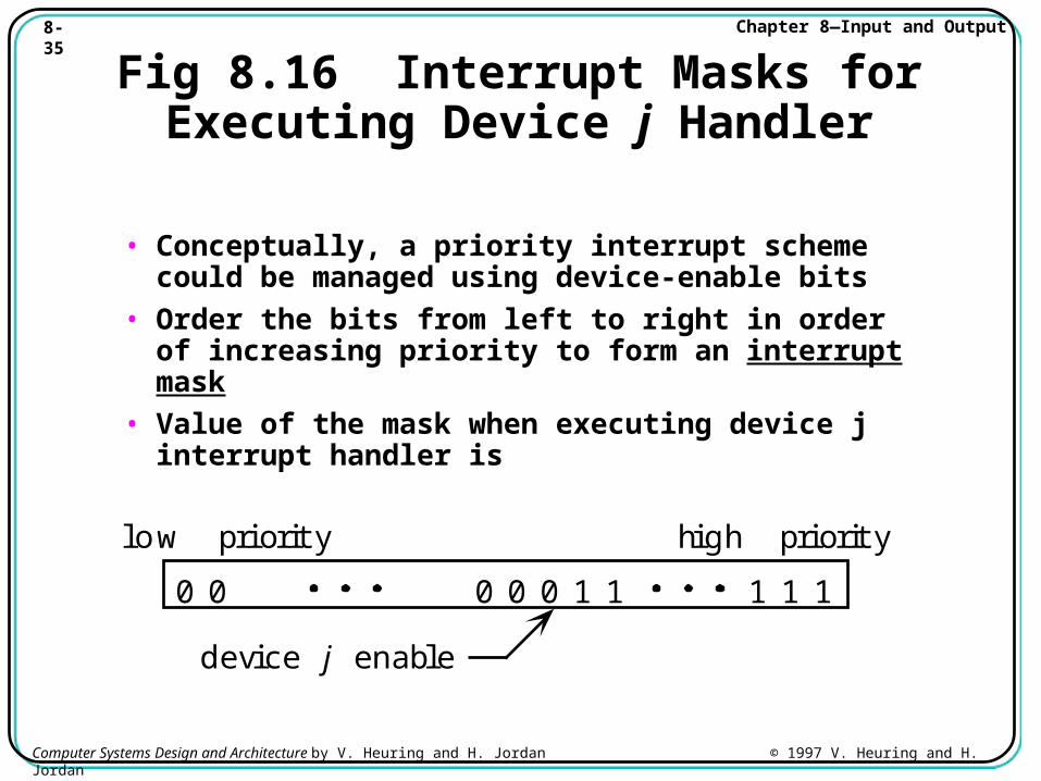
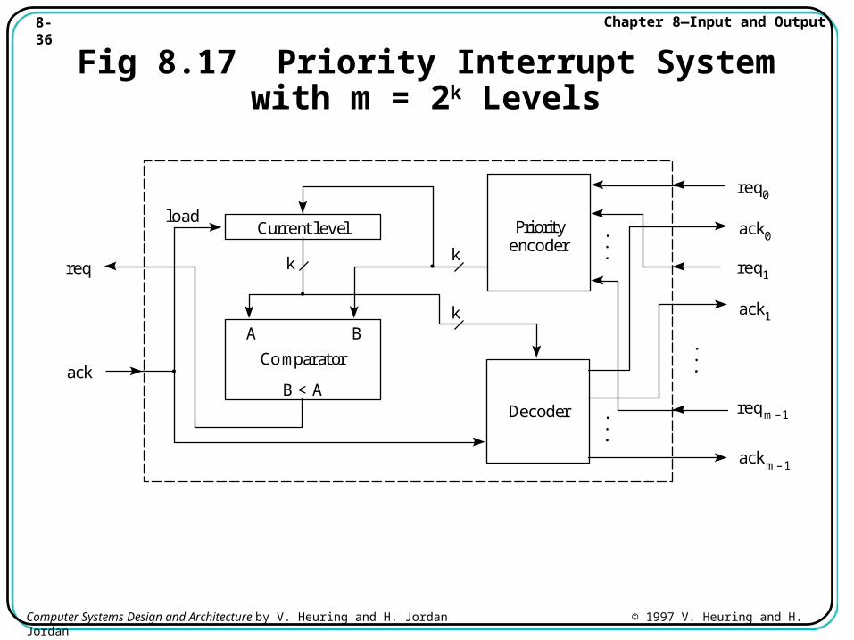
Fig 8.16 Interrupt Masks for Executing Device j Handler
• Conceptually, a priority interrupt scheme could be managed using device-enable bits
• Order the bits from left to right in order of increasing priority to form an interrupt mask
• Value of the mask when executing device j interrupt handler is
low priorit y high priorit y
device j enable
1 1 10 0 0 1 10 0
8-36 Chapter 8—Input and Output
Computer Systems Design and Architecture by V. Heuring and H. Jordan © 1997 V. Heuring and H. Jordan
Fig 8.17 Priority Interrupt System with m = 2k Levels
req
load
k
A B
Comparator
B < A
k
k
req0
ack0
req1
ack1
reqm –1
ackm –1
Decoder
Priorityencoder
Current level
ack
8-37 Chapter 8—Input and Output
Computer Systems Design and Architecture by V. Heuring and H. Jordan © 1997 V. Heuring and H. Jordan
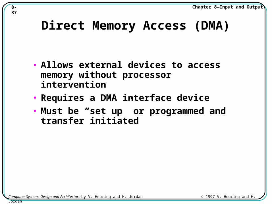
Direct Memory Access (DMA)
• Allows external devices to access memory without processor intervention
• Requires a DMA interface device
• Must be “set up” or programmed and transfer initiated
8-38 Chapter 8—Input and Output
Computer Systems Design and Architecture by V. Heuring and H. Jordan © 1997 V. Heuring and H. Jordan
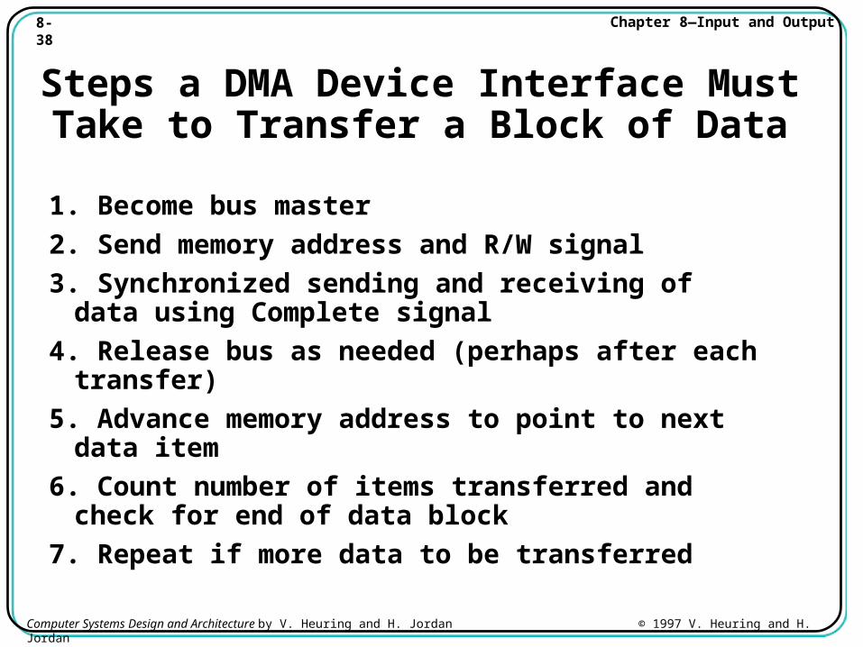
Steps a DMA Device Interface Must Take to Transfer a Block of Data
1. Become bus master
2. Send memory address and R/W signal
3. Synchronized sending and receiving of data using Complete signal
4. Release bus as needed (perhaps after each transfer)
5. Advance memory address to point to next data item
6. Count number of items transferred and check for end of data block
7. Repeat if more data to be transferred
8-39 Chapter 8—Input and Output
Computer Systems Design and Architecture by V. Heuring and H. Jordan © 1997 V. Heuring and H. Jordan
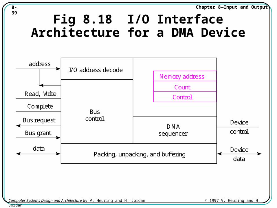
Fig 8.18 I/O Interface Architecture for a DMA Device
data Device
data
Device
controlBus grant
Bus request
Read, Write
Complete
addressI/O address decode
Buscontrol
Memory address
Count
Control
DMAsequencer
Packing, unpacking, and buffering
8-40 Chapter 8—Input and Output
Computer Systems Design and Architecture by V. Heuring and H. Jordan © 1997 V. Heuring and H. Jordan
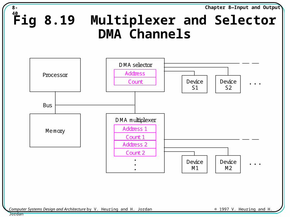
Fig 8.19 Multiplexer and Selector DMA Channels
Processor
Memory
DMA multiplexer
Bus
DMA selector
Count
Address
Count 1
Address 1
Count 2
Address 2
DeviceS1
DeviceS2
DeviceM1
DeviceM2
8-41 Chapter 8—Input and Output
Computer Systems Design and Architecture by V. Heuring and H. Jordan © 1997 V. Heuring and H. Jordan
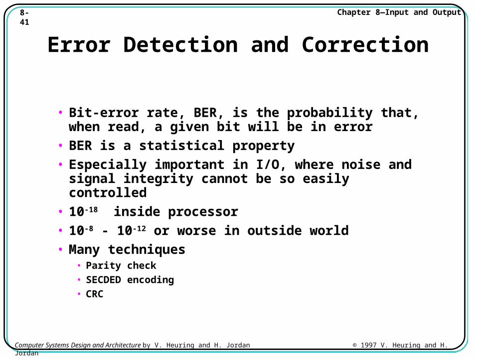
Error Detection and Correction
• Bit-error rate, BER, is the probability that, when read, a given bit will be in error
• BER is a statistical property
• Especially important in I/O, where noise and signal integrity cannot be so easily controlled
• 10-18 inside processor
• 10-8 - 10-12 or worse in outside world
• Many techniques• Parity check
• SECDED encoding
• CRC
8-42 Chapter 8—Input and Output
Computer Systems Design and Architecture by V. Heuring and H. Jordan © 1997 V. Heuring and H. Jordan
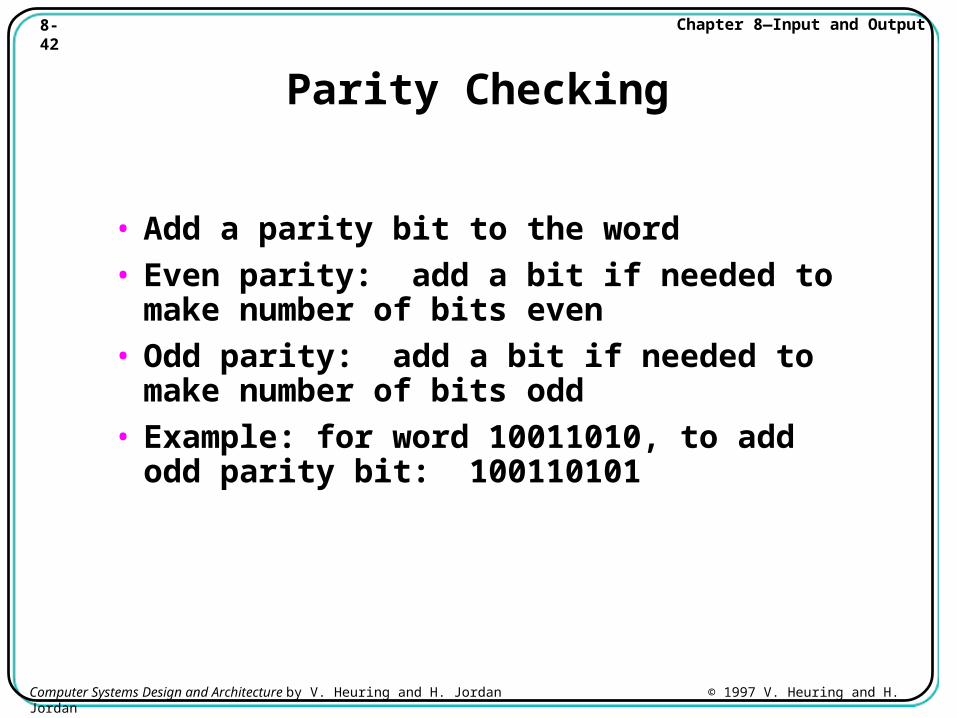
Parity Checking
• Add a parity bit to the word
• Even parity: add a bit if needed to make number of bits even
• Odd parity: add a bit if needed to make number of bits odd
• Example: for word 10011010, to add odd parity bit: 100110101
8-43 Chapter 8—Input and Output
Computer Systems Design and Architecture by V. Heuring and H. Jordan © 1997 V. Heuring and H. Jordan
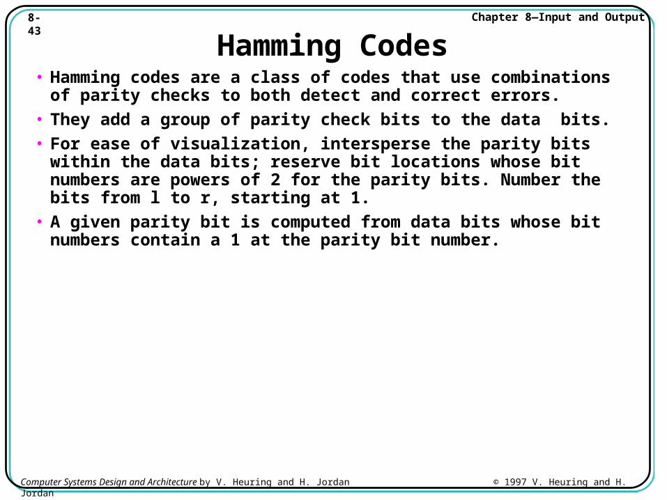
Hamming Codes• Hamming codes are a class of codes that use combinations
of parity checks to both detect and correct errors.
• They add a group of parity check bits to the data bits.
• For ease of visualization, intersperse the parity bits within the data bits; reserve bit locations whose bit numbers are powers of 2 for the parity bits. Number the bits from l to r, starting at 1.
• A given parity bit is computed from data bits whose bit numbers contain a 1 at the parity bit number.
8-44 Chapter 8—Input and Output
Computer Systems Design and Architecture by V. Heuring and H. Jordan © 1997 V. Heuring and H. Jordan
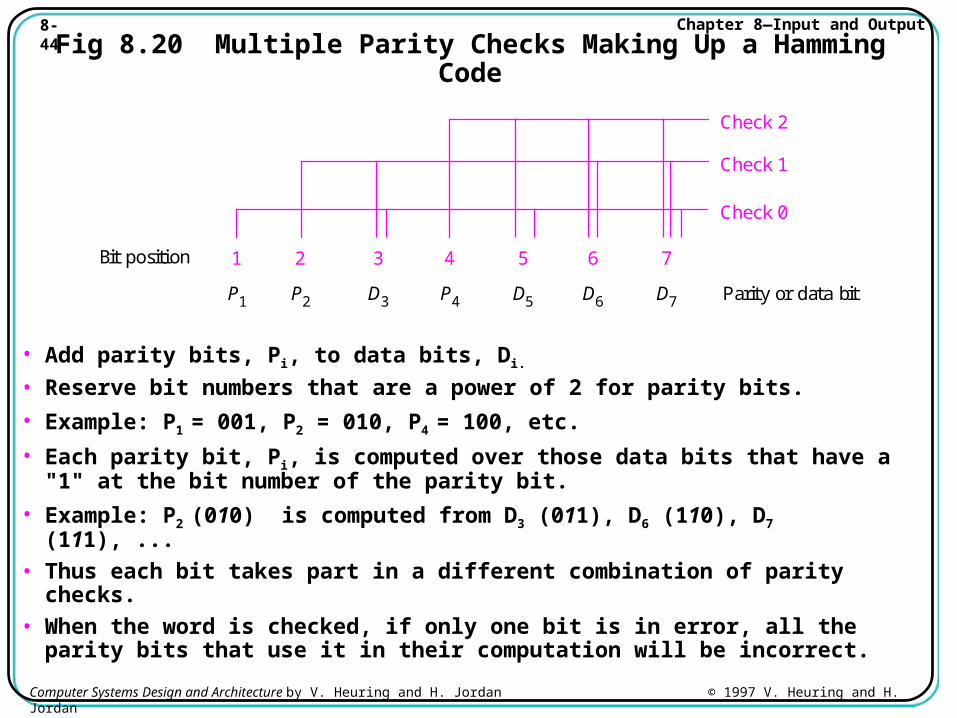
Fig 8.20 Multiple Parity Checks Making Up a Hamming Code
• Add parity bits, Pi, to data bits, Di.
• Reserve bit numbers that are a power of 2 for parity bits.
• Example: P1 = 001, P2 = 010, P4 = 100, etc.
• Each parity bit, Pi, is computed over those data bits that have a "1" at the bit number of the parity bit.
• Example: P2 (010) is computed from D3 (011), D6 (110), D7 (111), ...
• Thus each bit takes part in a different combination of parity checks.
• When the word is checked, if only one bit is in error, all the parity bits that use it in their computation will be incorrect.
Bit position
P1
1
P2
2
D3
3
P4
4
D5
5
D6
6
D7 Parity or data bit
7
Check 0
Check 1
Check 2
8-45 Chapter 8—Input and Output
Computer Systems Design and Architecture by V. Heuring and H. Jordan © 1997 V. Heuring and H. Jordan
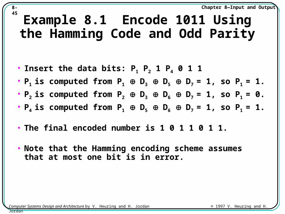
Example 8.1 Encode 1011 Using the Hamming Code and Odd Parity
• Insert the data bits: P1 P2 1 P4 0 1 1
• P1 is computed from P1 D3 D5 D7 = 1, so P1 = 1.
• P2 is computed from P2 D3 D6 D7 = 1, so P1 = 0.
• P4 is computed from P1 D5 D6 D7 = 1, so P1 = 1.
• The final encoded number is 1 0 1 1 0 1 1.
• Note that the Hamming encoding scheme assumes that at most one bit is in error.
8-46 Chapter 8—Input and Output
Computer Systems Design and Architecture by V. Heuring and H. Jordan © 1997 V. Heuring and H. Jordan
SECDED (Single Error Correct, Double Error Detect)
• Add another parity bit, at position 0, which is computed to make the parity over all bits, data and parity, even or odd.
• If one bit is in error, a unique set of Hamming checks will fail, and the overall parity will also be wrong.
• Let ci be true if check i fails, otherwise true.
• In the case of a 1-bit error, the string ck-1, . . ., c1, c0 will be the binary index of the erroneous bit.
• For example, if the ci string is 0110, then bit at position 6 is in error.
• If two bits are in error, one or more Hamming checks will fail, but the overall parity will be correct.
• Thus the failure of one or more Hamming checks, coupled with correct overall parity, means that 2 bits are in error.
• This assumes that the probability of 3 or more bits being in error is negligible.
8-47 Chapter 8—Input and Output
Computer Systems Design and Architecture by V. Heuring and H. Jordan © 1997 V. Heuring and H. Jordan
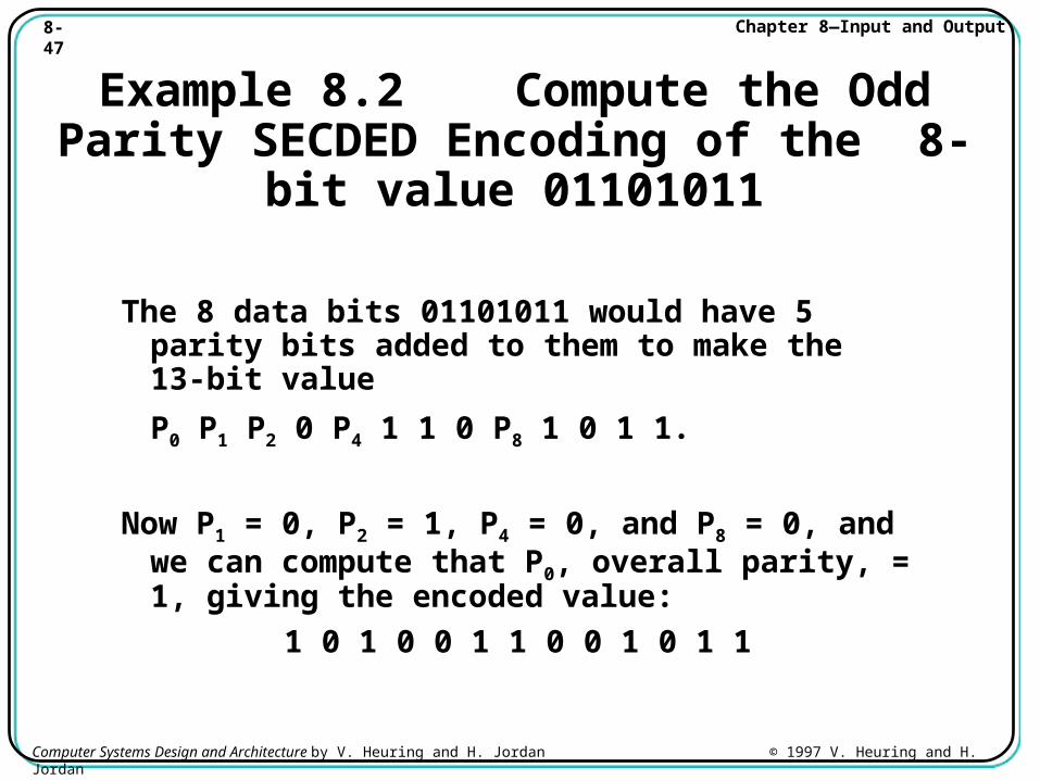
Example 8.2 Compute the Odd Parity SECDED Encoding of the 8-bit value
01101011
The 8 data bits 01101011 would have 5 parity bits added to them to make the 13-bit value
P0 P1 P2 0 P4 1 1 0 P8 1 0 1 1.
Now P1 = 0, P2 = 1, P4 = 0, and P8 = 0, and we can compute that P0, overall parity, = 1, giving the encoded value:
1 0 1 0 0 1 1 0 0 1 0 1 1
8-48 Chapter 8—Input and Output
Computer Systems Design and Architecture by V. Heuring and H. Jordan © 1997 V. Heuring and H. Jordan
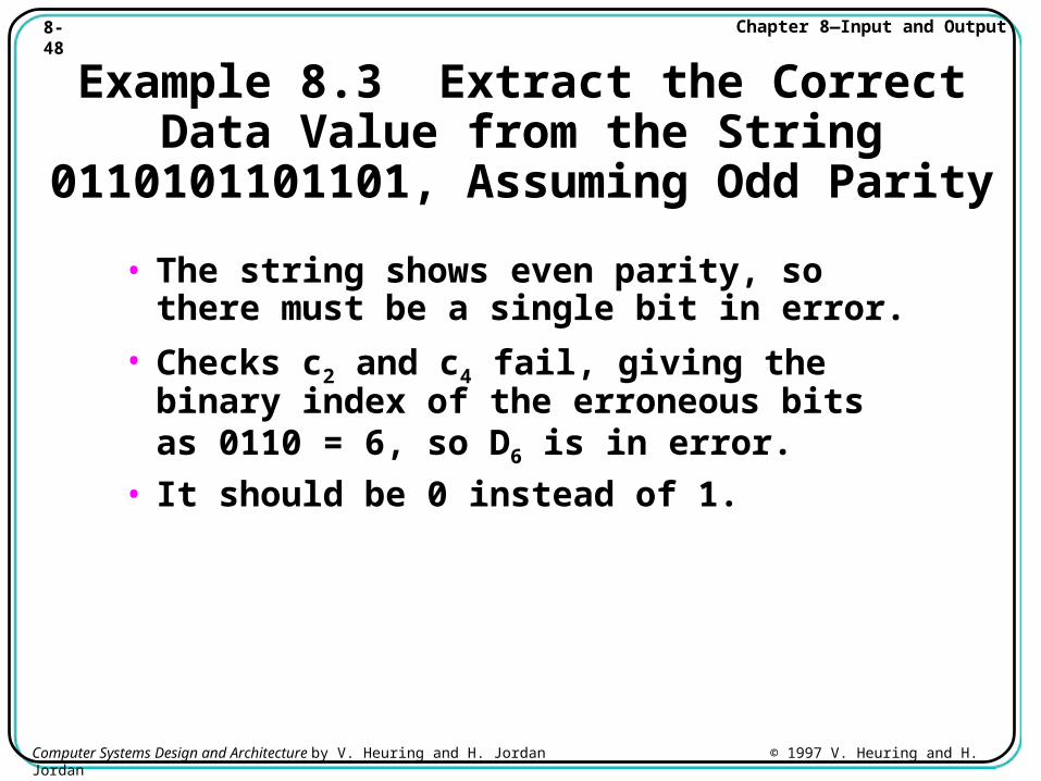
Example 8.3 Extract the Correct Data Value from the String 0110101101101,
Assuming Odd Parity
• The string shows even parity, so there must be a single bit in error.
• Checks c2 and c4 fail, giving the binary index of the erroneous bits as 0110 = 6, so D6 is in error.
• It should be 0 instead of 1.
8-49 Chapter 8—Input and Output
Computer Systems Design and Architecture by V. Heuring and H. Jordan © 1997 V. Heuring and H. Jordan
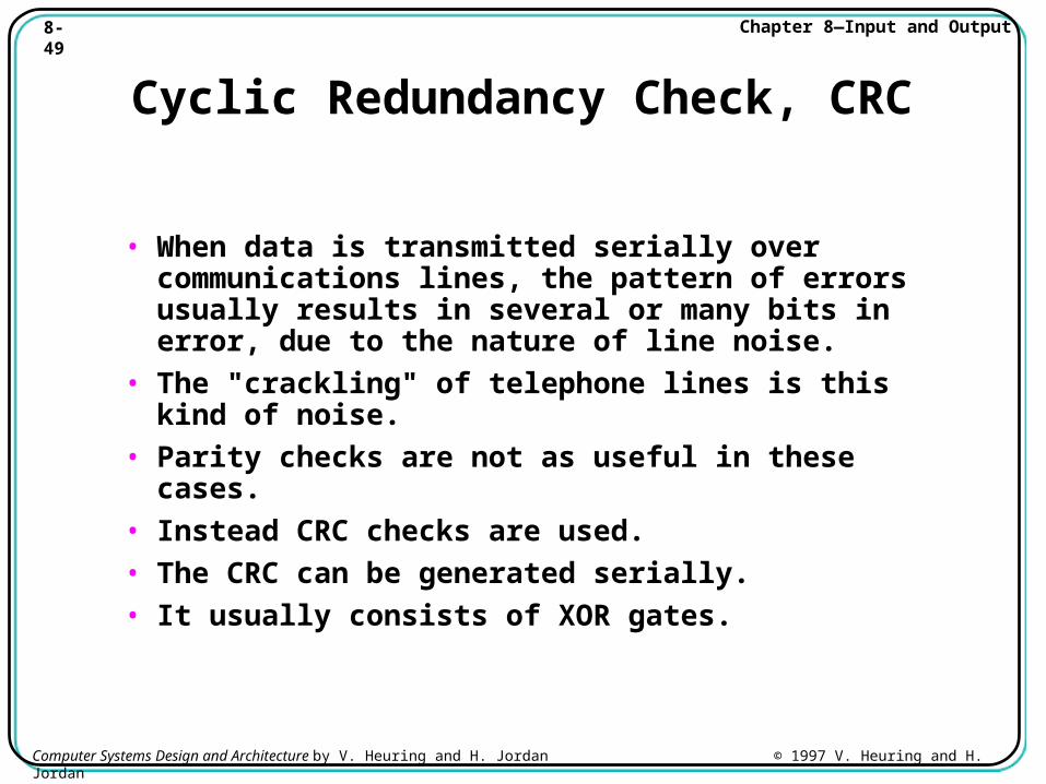
Cyclic Redundancy Check, CRC
• When data is transmitted serially over communications lines, the pattern of errors usually results in several or many bits in error, due to the nature of line noise.
• The "crackling" of telephone lines is this kind of noise.
• Parity checks are not as useful in these cases.
• Instead CRC checks are used.
• The CRC can be generated serially.
• It usually consists of XOR gates.
8-50 Chapter 8—Input and Output
Computer Systems Design and Architecture by V. Heuring and H. Jordan © 1997 V. Heuring and H. Jordan
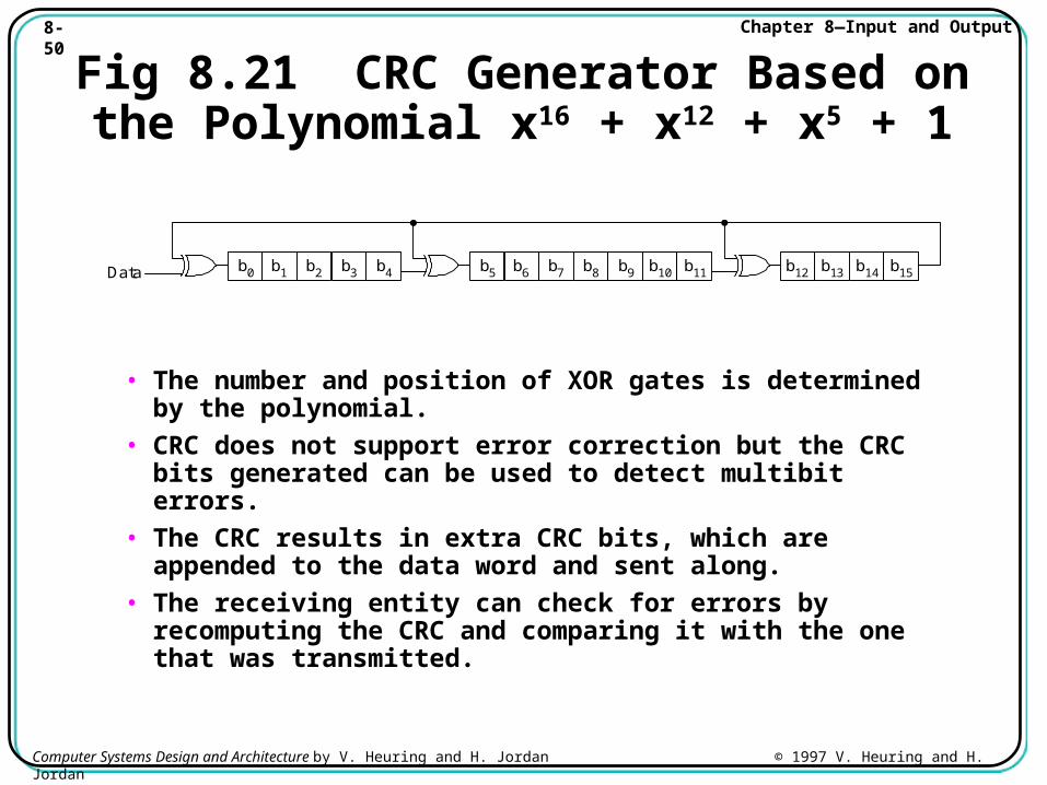
Fig 8.21 CRC Generator Based on the Polynomial x16 + x12 + x5 + 1
• The number and position of XOR gates is determined by the polynomial.
• CRC does not support error correction but the CRC bits generated can be used to detect multibit errors.
• The CRC results in extra CRC bits, which are appended to the data word and sent along.
• The receiving entity can check for errors by recomputing the CRC and comparing it with the one that was transmitted.
b0Data b1 b2 b3 b4 b5 b6 b7 b8 b9 b10 b11 b12 b13 b14 b15
8-51 Chapter 8—Input and Output
Computer Systems Design and Architecture by V. Heuring and H. Jordan © 1997 V. Heuring and H. Jordan
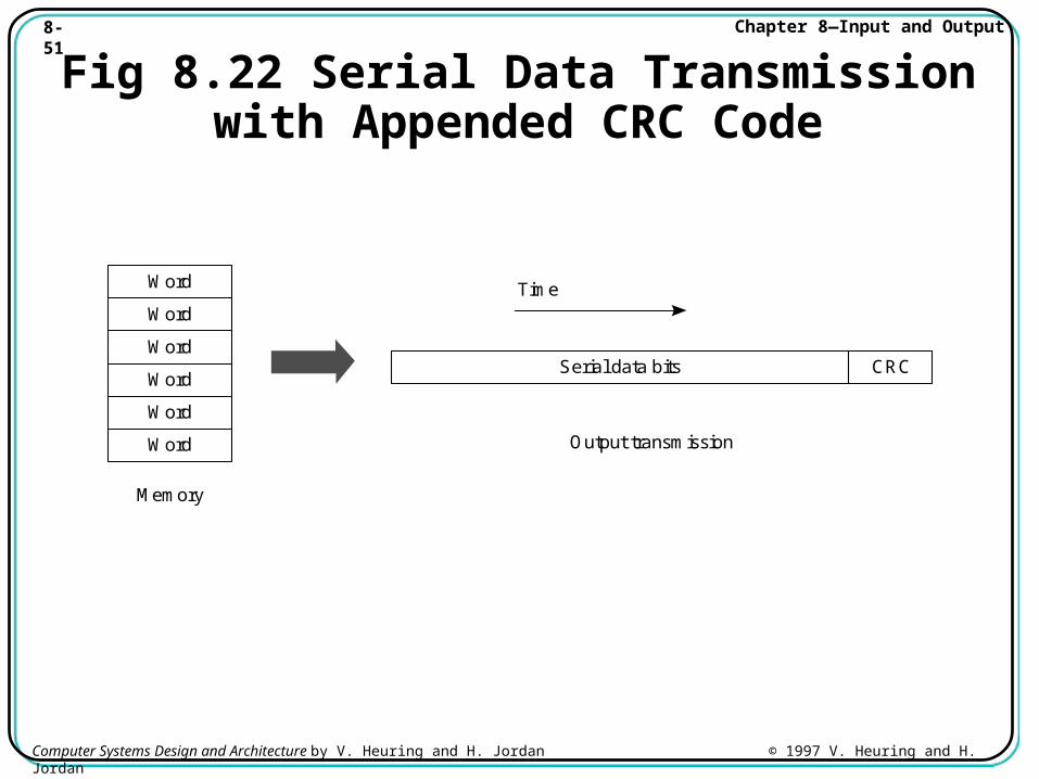
Fig 8.22 Serial Data Transmission with Appended CRC Code
Word Time
Output transmission
Serial data bits
Word
Word
Word
Word
Word
Memory
CRC
8-52 Chapter 8—Input and Output
Computer Systems Design and Architecture by V. Heuring and H. Jordan © 1997 V. Heuring and H. Jordan
Chapter 8 Summary
• I/O subsystem has characteristics that make it different from main memory
• Speed variations
• Latency
• Band width
• This leads to 3 different kinds of I/O:• Programmed I/O handled completely by software, from
initiation until completion
• Interrupt-driven I/O combines hardware for initiation and software for completion
• DMA allows an all-hardware approach to I/O activities
• External connections to devices may require data format changes, and error detection and possibly correction