Embed Size (px)
Citation preview

aPreliminary Technical Data
TigerSHARC and the TigerSHARC logo are registered trademarks of Analog Devices, Inc.
Blackfin®
Embedded ProcessorADSP-BF536/ADSP-BF537
Rev. PrEInformation furnished by Analog Devices is believed to be accurate and reliable.However, no responsibility is assumed by Analog Devices for its use, nor for anyinfringements of patents or other rights of third parties that may result from its use.Specifications subject to change without notice. No license is granted by implicationor otherwise under any patent or patent rights of Analog Devices. Trademarks andregistered trademarks are the property of their respective owners.
One Technology Way, P.O.Box 9106, Norwood, MA 02062-9106 U.S.A.Tel:781/329-4700 www.analog.comFax:781/461-3113 © 2005 Analog Devices, Inc. All rights reserved.
FEATURES
Up to 600 MHz High-Performance Blackfin Processor Two 16-Bit MACs, Two 40-Bit ALUs, Four 8-Bit Video
ALUs, 40-Bit Shifter
RISC-Like Register and Instruction Model for Ease of Programming and Compiler-Friendly Support
Advanced Debug, Trace, and Performance-Monitoring0.8 V to 1.2 V Core VDD with On-chip Voltage Regulation2.5 V and 3.3 V-Tolerant I/O with Specific 5 V-Tolerant Pins 182-Ball MBGA and 208-Ball Sparse MBGA PackagesLead Bearing and Lead Free Package Choices
MEMORY
Up to 132K Bytes of On-Chip Memory: 16K Bytes of Instruction SRAM/Cache48K Bytes of Instruction SRAM32K Bytes of Data SRAM/Cache32K Bytes of Data SRAM4K Bytes of Scratchpad SRAM
External Memory Controller with Glueless Support for SDRAM and Asynchronous 8/16-Bit Memories
Flexible Booting Options from External Flash, SPI and TWI Memory or from SPI, TWI, and UART Host Devices
Two Dual-Channel Memory DMA ControllersMemory Management Unit Providing Memory Protection
PERIPHERALS
IEEE 802.3-Compliant 10/100 Ethernet MAC Controller Area Network (CAN) 2.0B InterfaceParallel Peripheral Interface (PPI), Supporting ITU-R 656
Video Data FormatsTwo Dual-Channel, Full-Duplex Synchronous Serial Ports
(SPORTs), Supporting Eight Stereo I2S Channels 12 Peripheral DMAs, 2 Mastered by the Ethernet MACTwo Memory-to-Memory DMAs With External Request LinesEvent Handler With 32 Interrupt InputsSerial Peripheral Interface (SPI)-CompatibleTwo UARTs with IrDA® Support Two-Wire Interface (TWI) ControllerEight 32-Bit Timer/Counters with PWM SupportReal-Time Clock (RTC) and Watchdog Timer32-Bit Core Timer48 General-Purpose I/Os (GPIOs), 8 with High Current DriversOn-Chip PLL Capable of 1x to 63x Frequency MultiplicationDebug/JTAG Interface
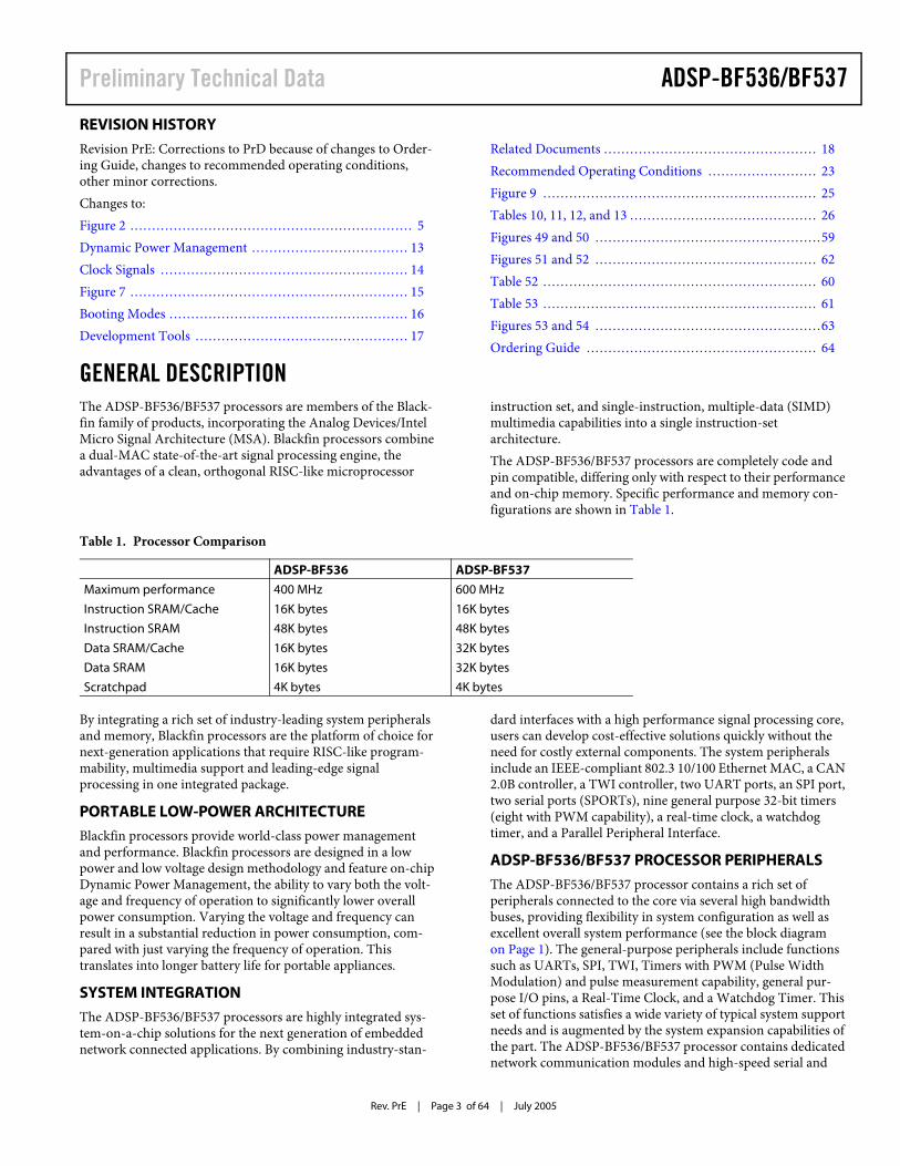
Figure 1. Functional Block Diagram
VOLTAGEREGULATOR
DMACONTROLLER
EVENTCONTROLLER/CORE TIMER
ETHERNET MAC
UART 0-1
TIMERS 0-7
PPI
SPORT1
SPI
EXTERNAL PORTFLASH, SDRAM
CONTROL
BOOT ROM
JTAG TEST ANDEMULATION WATCHDOG TIMER
L1INSTRUCTION
MEMORY
L1DATA
MEMORYMMU
B
CORE / SYSTEM BUS INTERFACE
RTC
TWI
CAN
SPORT0
GPIOPORT
F
GPIOPORT
H
GPIOPORT
G
PORTJ

Rev. PrE | Page 2 of 64 | July 2005
ADSP-BF536/BF537 Preliminary Technical Data
TABLE OF CONTENTSGeneral Description . . . . . . . . . . . . . . . . . . . . . . . . . . . . . . . . . . . . . . . . . . . . . . . . . 3
Portable Low-Power Architecture . . . . . . . . . . . . . . . . . . . . . . . . . . . . . 3System Integration . . . . . . . . . . . . . . . . . . . . . . . . . . . . . . . . . . . . . . . . . . . . . . . . 3ADSP-BF536/BF537 Processor Peripherals . . . . . . . . . . . . . . . . . 3Blackfin Processor Core . . . . . . . . . . . . . . . . . . . . . . . . . . . . . . . . . . . . . . . . . . 4Memory Architecture . . . . . . . . . . . . . . . . . . . . . . . . . . . . . . . . . . . . . . . . . . . . 4
Internal (On-chip) Memory . . . . . . . . . . . . . . . . . . . . . . . . . . . . . . . . . 5External (Off-Chip) Memory . . . . . . . . . . . . . . . . . . . . . . . . . . . . . . . . 5I/O Memory Space . . . . . . . . . . . . . . . . . . . . . . . . . . . . . . . . . . . . . . . . . . . . . 6Booting . . . . . . . . . . . . . . . . . . . . . . . . . . . . . . . . . . . . . . . . . . . . . . . . . . . . . . . . . . . 6Event Handling . . . . . . . . . . . . . . . . . . . . . . . . . . . . . . . . . . . . . . . . . . . . . . . . . 6Core Event Controller (CEC) . . . . . . . . . . . . . . . . . . . . . . . . . . . . . . . . 7System Interrupt Controller (SIC) . . . . . . . . . . . . . . . . . . . . . . . . . . 7Event Control . . . . . . . . . . . . . . . . . . . . . . . . . . . . . . . . . . . . . . . . . . . . . . . . . . . 8
DMA Controllers . . . . . . . . . . . . . . . . . . . . . . . . . . . . . . . . . . . . . . . . . . . . . . . . . . 8Real-Time Clock . . . . . . . . . . . . . . . . . . . . . . . . . . . . . . . . . . . . . . . . . . . . . . . . . . . 9Watchdog Timer . . . . . . . . . . . . . . . . . . . . . . . . . . . . . . . . . . . . . . . . . . . . . . . . . . 9Timers . . . . . . . . . . . . . . . . . . . . . . . . . . . . . . . . . . . . . . . . . . . . . . . . . . . . . . . . . . . . . 10Serial Ports (SPORTs) . . . . . . . . . . . . . . . . . . . . . . . . . . . . . . . . . . . . . . . . . . 10Serial Peripheral Interface (SPI) Port . . . . . . . . . . . . . . . . . . . . . . . 10UART Ports (UARTs) . . . . . . . . . . . . . . . . . . . . . . . . . . . . . . . . . . . . . . . . . . 11Controller Area Network (CAN) . . . . . . . . . . . . . . . . . . . . . . . . . . . . 11TWI Controller Interface . . . . . . . . . . . . . . . . . . . . . . . . . . . . . . . . . . . . . . 1110/100 Ethernet MAC .. . . . . . . . . . . . . . . . . . . . . . . . . . . . . . . . . . . . . . . . . 11Ports . . . . . . . . . . . . . . . . . . . . . . . . . . . . . . . . . . . . . . . . . . . . . . . . . . . . . . . . . . . . . . . . 12
General-Purpose I/O (GPIO) . . . . . . . . . . . . . . . . . . . . . . . . . . . . . . 12Parallel Peripheral Interface (PPI) . . . . . . . . . . . . . . . . . . . . . . . . . . . 13Dynamic Power Management . . . . . . . . . . . . . . . . . . . . . . . . . . . . . . . . 13
Full-On Operating Mode – Maximum Performance . 13Active Operating Mode – Moderate Power Savings . . 13Sleep Operating Mode – High Dynamic
Power Savings . . . . . . . . . . . . . . . . . . . . . . . . . . . . . . . . . . . . . . . . . . . . . . 13Deep Sleep Operating Mode – Maximum Dynamic
Power Savings . . . . . . . . . . . . . . . . . . . . . . . . . . . . . . . . . . . . . . . . . . . . . . 13Hibernate Operating Mode – Maximum Static Power
Savings . . . . . . . . . . . . . . . . . . . . . . . . . . . . . . . . . . . . . . . . . . . . . . . . . . . . . . . 14Power Savings . . . . . . . . . . . . . . . . . . . . . . . . . . . . . . . . . . . . . . . . . . . . . . . . . 14
Voltage Regulation . . . . . . . . . . . . . . . . . . . . . . . . . . . . . . . . . . . . . . . . . . . . . . 14Clock Signals . . . . . . . . . . . . . . . . . . . . . . . . . . . . . . . . . . . . . . . . . . . . . . . . . . . . . 14Booting Modes . . . . . . . . . . . . . . . . . . . . . . . . . . . . . . . . . . . . . . . . . . . . . . . . . . . 16Instruction Set Description . . . . . . . . . . . . . . . . . . . . . . . . . . . . . . . . . . . 17Development Tools . . . . . . . . . . . . . . . . . . . . . . . . . . . . . . . . . . . . . . . . . . . . . 17
EZ-KIT Lite Evaluation Board . . . . . . . . . . . . . . . . . . . . . . . . . . . . . 17Designing an Emulator-Compatible Processor
Board (Target) . . . . . . . . . . . . . . . . . . . . . . . . . . . . . . . . . . . . . . . . . . . . . . . . . 17Related Documents . . . . . . . . . . . . . . . . . . . . . . . . . . . . . . . . . . . . . . . . . . . . . . 18
Pin Descriptions . . . . . . . . . . . . . . . . . . . . . . . . . . . . . . . . . . . . . . . . . . . . . . . . . . . . 19Specifications . . . . . . . . . . . . . . . . . . . . . . . . . . . . . . . . . . . . . . . . . . . . . . . . . . . . . . . . 23
Recommended Operating Conditions . . . . . . . . . . . . . . . . . . . . . . 23Absolute Maximum Ratings . . . . . . . . . . . . . . . . . . . . . . . . . . . . . . . . . . . 25ESD Sensitivity . . . . . . . . . . . . . . . . . . . . . . . . . . . . . . . . . . . . . . . . . . . . . . . . . . . 25Timing Specifications . . . . . . . . . . . . . . . . . . . . . . . . . . . . . . . . . . . . . . . . . . . 26
Asynchronous Memory Read Cycle Timing . . . . . . . . . . . . 28Asynchronous Memory Write Cycle Timing . . . . . . . . . . . 29SDRAM Interface Timing . . . . . . . . . . . . . . . . . . . . . . . . . . . . . . . . . . 30External Port Bus Request and Grant Cycle Timing . . 31External DMA Request Timing . . . . . . . . . . . . . . . . . . . . . . . . . . . . 32Parallel Peripheral Interface Timing . . . . . . . . . . . . . . . . . . . . . . 33Serial Ports . . . . . . . . . . . . . . . . . . . . . . . . . . . . . . . . . . . . . . . . . . . . . . . . . . . . . 34Serial Peripheral Interface (SPI) Port—
Master Timing . . . . . . . . . . . . . . . . . . . . . . . . . . . . . . . . . . . . . . . . . . . . . . 39Serial Peripheral Interface (SPI) Port—
Slave Timing . . . . . . . . . . . . . . . . . . . . . . . . . . . . . . . . . . . . . . . . . . . . . . . . 40Universal Asynchronous Receiver-Transmitter
(UART) Ports—Receive and Transmit Timing . . . . . 41General-Purpose Port Timing . . . . . . . . . . . . . . . . . . . . . . . . . . . . . 42Timer Cycle Timing . . . . . . . . . . . . . . . . . . . . . . . . . . . . . . . . . . . . . . . . . . 43JTAG Test And Emulation Port Timing . . . . . . . . . . . . . . . . . 44TWI Controller Timing . . . . . . . . . . . . . . . . . . . . . . . . . . . . . . . . . . . . . 4510/100 Ethernet MAC Controller Timing . . . . . . . . . . . . . . . 49
Output Drive Currents . . . . . . . . . . . . . . . . . . . . . . . . . . . . . . . . . . . . . . . . . 52Power Dissipation . . . . . . . . . . . . . . . . . . . . . . . . . . . . . . . . . . . . . . . . . . . . . . . 55Test Conditions . . . . . . . . . . . . . . . . . . . . . . . . . . . . . . . . . . . . . . . . . . . . . . . . . . 55
Output Enable Time . . . . . . . . . . . . . . . . . . . . . . . . . . . . . . . . . . . . . . . . . 55Output Disable Time . . . . . . . . . . . . . . . . . . . . . . . . . . . . . . . . . . . . . . . . . 55Example System Hold Time Calculation . . . . . . . . . . . . . . . . 56
Environmental Conditions . . . . . . . . . . . . . . . . . . . . . . . . . . . . . . . . . . . . 56182-Ball Mini-BGA Pinout . . . . . . . . . . . . . . . . . . . . . . . . . . . . . . . . . . . . . . . 57208-Ball Sparse Mini-BGA Pinout . . . . . . . . . . . . . . . . . . . . . . . . . . . . . . 60Outline Dimensions . . . . . . . . . . . . . . . . . . . . . . . . . . . . . . . . . . . . . . . . . . . . . . . . 63Ordering Guide . . . . . . . . . . . . . . . . . . . . . . . . . . . . . . . . . . . . . . . . . . . . . . . . . . . . . 64
ADSP-BF536/BF537Preliminary Technical Data
Rev. PrE | Page 3 of 64 | July 2005
REVISION HISTORY
Revision PrE: Corrections to PrD because of changes to Order-ing Guide, changes to recommended operating conditions, other minor corrections.Changes to:Figure 2 . . . . . . . . . . . . . . . . . . . . . . . . . . . . . . . . . . . . . . . . . . . . . . . . . . . . . . . . . . . . . . . . . 5Dynamic Power Management . . . . . . . . . . . . . . . . . . . . . . . . . . . . . . . . . . . . 13Clock Signals . . . . . . . . . . . . . . . . . . . . . . . . . . . . . . . . . . . . . . . . . . . . . . . . . . . . . . . . . 14Figure 7 . . . . . . . . . . . . . . . . . . . . . . . . . . . . . . . . . . . . . . . . . . . . . . . . . . . . . . . . . . . . . . . . 15Booting Modes . . . . . . . . . . . . . . . . . . . . . . . . . . . . . . . . . . . . . . . . . . . . . . . . . . . . . . . 16Development Tools . . . . . . . . . . . . . . . . . . . . . . . . . . . . . . . . . . . . . . . . . . . . . . . . . 17
Related Documents . . . . . . . . . . . . . . . . . . . . . . . . . . . . . . . . . . . . . . . . . . . . . . . . . 18Recommended Operating Conditions . . . . . . . . . . . . . . . . . . . . . . . . . 23Figure 9 . . . . . . . . . . . . . . . . . . . . . . . . . . . . . . . . . . . . . . . . . . . . . . . . . . . . . . . . . . . . . . . 25Tables 10, 11, 12, and 13 . . . . . . . . . . . . . . . . . . . . . . . . . . . . . . . . . . . . . . . . . . . 26Figures 49 and 50 . . . . . . . . . . . . . . . . . . . . . . . . . . . . . . . . . . . . . . . . . . . . . . . . . . . .59 Figures 51 and 52 . . . . . . . . . . . . . . . . . . . . . . . . . . . . . . . . . . . . . . . . . . . . . . . . . . . 62Table 52 . . . . . . . . . . . . . . . . . . . . . . . . . . . . . . . . . . . . . . . . . . . . . . . . . . . . . . . . . . . . . . . 60Table 53 . . . . . . . . . . . . . . . . . . . . . . . . . . . . . . . . . . . . . . . . . . . . . . . . . . . . . . . . . . . . . . . 61Figures 53 and 54 . . . . . . . . . . . . . . . . . . . . . . . . . . . . . . . . . . . . . . . . . . . . . . . . . . . .63 Ordering Guide . . . . . . . . . . . . . . . . . . . . . . . . . . . . . . . . . . . . . . . . . . . . . . . . . . . . . 64
GENERAL DESCRIPTIONThe ADSP-BF536/BF537 processors are members of the Black-fin family of products, incorporating the Analog Devices/Intel Micro Signal Architecture (MSA). Blackfin processors combine a dual-MAC state-of-the-art signal processing engine, the advantages of a clean, orthogonal RISC-like microprocessor
instruction set, and single-instruction, multiple-data (SIMD) multimedia capabilities into a single instruction-set architecture.The ADSP-BF536/BF537 processors are completely code and pin compatible, differing only with respect to their performance and on-chip memory. Specific performance and memory con-figurations are shown in Table 1.
By integrating a rich set of industry-leading system peripherals and memory, Blackfin processors are the platform of choice for next-generation applications that require RISC-like program-mability, multimedia support and leading-edge signal processing in one integrated package.
PORTABLE LOW-POWER ARCHITECTURE
Blackfin processors provide world-class power management and performance. Blackfin processors are designed in a low power and low voltage design methodology and feature on-chip Dynamic Power Management, the ability to vary both the volt-age and frequency of operation to significantly lower overall power consumption. Varying the voltage and frequency can result in a substantial reduction in power consumption, com-pared with just varying the frequency of operation. This translates into longer battery life for portable appliances.
SYSTEM INTEGRATION
The ADSP-BF536/BF537 processors are highly integrated sys-tem-on-a-chip solutions for the next generation of embedded network connected applications. By combining industry-stan-
dard interfaces with a high performance signal processing core, users can develop cost-effective solutions quickly without the need for costly external components. The system peripherals include an IEEE-compliant 802.3 10/100 Ethernet MAC, a CAN 2.0B controller, a TWI controller, two UART ports, an SPI port, two serial ports (SPORTs), nine general purpose 32-bit timers (eight with PWM capability), a real-time clock, a watchdog timer, and a Parallel Peripheral Interface.
ADSP-BF536/BF537 PROCESSOR PERIPHERALS
The ADSP-BF536/BF537 processor contains a rich set of peripherals connected to the core via several high bandwidth buses, providing flexibility in system configuration as well as excellent overall system performance (see the block diagram on Page 1). The general-purpose peripherals include functions such as UARTs, SPI, TWI, Timers with PWM (Pulse Width Modulation) and pulse measurement capability, general pur-pose I/O pins, a Real-Time Clock, and a Watchdog Timer. This set of functions satisfies a wide variety of typical system support needs and is augmented by the system expansion capabilities of the part. The ADSP-BF536/BF537 processor contains dedicated network communication modules and high-speed serial and
Table 1. Processor Comparison
ADSP-BF536 ADSP-BF537
Maximum performance 400 MHz 600 MHz
Instruction SRAM/Cache 16K bytes 16K bytes
Instruction SRAM 48K bytes 48K bytes
Data SRAM/Cache 16K bytes 32K bytes
Data SRAM 16K bytes 32K bytes
Scratchpad 4K bytes 4K bytes
Rev. PrE | Page 4 of 64 | July 2005
ADSP-BF536/BF537 Preliminary Technical Data
parallel ports, an interrupt controller for flexible management of interrupts from the on-chip peripherals or external sources, and power management control functions to tailor the perfor-mance and power characteristics of the processor and system to many application scenarios.All of the peripherals, except for general-purpose I/O, CAN, TWI, Real-Time Clock, and timers, are supported by a flexible DMA structure. There are also separate memory DMA channels dedicated to data transfers between the processor's various memory spaces, including external SDRAM and asynchronous memory. Multiple on-chip buses running at up to 133 MHz provide enough bandwidth to keep the processor core running along with activity on all of the on-chip and external peripherals.The ADSP-BF536/BF537 processor includes an on-chip voltage regulator in support of the ADSP-BF536/BF537 processor Dynamic Power Management capability. The voltage regulator provides a range of core voltage levels when supplied from a sin-gle 2.25 V to 3.6 V input. The voltage regulator can be bypassed at the user's discretion.
BLACKFIN PROCESSOR CORE
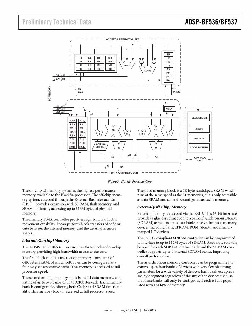
As shown in Figure 2 on Page 5, the Blackfin processor core contains two 16-bit multipliers, two 40-bit accumulators, two 40-bit ALUs, four video ALUs, and a 40-bit shifter. The compu-tation units process 8-bit, 16-bit, or 32-bit data from the register file.The compute register file contains eight 32-bit registers. When performing compute operations on 16-bit operand data, the register file operates as 16 independent 16-bit registers. All operands for compute operations come from the multiported register file and instruction constant fields.Each MAC can perform a 16-bit by 16-bit multiply in each cycle, accumulating the results into the 40-bit accumulators. Signed and unsigned formats, rounding, and saturation are supported.The ALUs perform a traditional set of arithmetic and logical operations on 16-bit or 32-bit data. In addition, many special instructions are included to accelerate various signal processing tasks. These include bit operations such as field extract and pop-ulation count, modulo 232 multiply, divide primitives, saturation and rounding, and sign/exponent detection. The set of video instructions include byte alignment and packing operations, 16-bit and 8-bit adds with clipping, 8-bit average operations, and 8-bit subtract/absolute value/accumulate (SAA) operations. Also provided are the compare/select and vector search instructions.For certain instructions, two 16-bit ALU operations can be per-formed simultaneously on register pairs (a 16-bit high half and 16-bit low half of a compute register). By also using the second ALU, quad 16-bit operations are possible.The 40-bit shifter can perform shifts and rotates and is used to support normalization, field extract, and field deposit instructions.
The program sequencer controls the flow of instruction execu-tion, including instruction alignment and decoding. For program flow control, the sequencer supports PC relative and indirect conditional jumps (with static branch prediction), and subroutine calls. Hardware is provided to support zero-over-head looping. The architecture is fully interlocked, meaning that the programmer need not manage the pipeline when executing instructions with data dependencies.The address arithmetic unit provides two addresses for simulta-neous dual fetches from memory. It contains a multiported register file consisting of four sets of 32-bit Index, Modify, Length, and Base registers (for circular buffering), and eight additional 32-bit pointer registers (for C-style indexed stack manipulation).Blackfin processors support a modified Harvard architecture in combination with a hierarchical memory structure. Level 1 (L1) memories are those that typically operate at the full processor speed with little or no latency. At the L1 level, the instruction memory holds instructions only. The two data memories hold data, and a dedicated scratchpad data memory stores stack and local variable information.In addition, multiple L1 memory blocks are provided, offering a configurable mix of SRAM and cache. The Memory Manage-ment Unit (MMU) provides memory protection for individual tasks that may be operating on the core and can protect system registers from unintended access.The architecture provides three modes of operation: User mode, Supervisor mode, and Emulation mode. User mode has restricted access to certain system resources, thus providing a protected software environment, while Supervisor mode has unrestricted access to the system and core resources.The Blackfin processor instruction set has been optimized so that 16-bit opcodes represent the most frequently used instruc-tions, resulting in excellent compiled code density. Complex DSP instructions are encoded into 32-bit opcodes, representing fully featured multifunction instructions. Blackfin processors support a limited multi-issue capability, where a 32-bit instruc-tion can be issued in parallel with two 16-bit instructions, allowing the programmer to use many of the core resources in a single instruction cycle.The Blackfin processor assembly language uses an algebraic syn-tax for ease of coding and readability. The architecture has been optimized for use in conjunction with the C/C++ compiler, resulting in fast and efficient software implementations.
MEMORY ARCHITECTURE
The ADSP-BF536/BF537 processor views memory as a single unified 4G byte address space, using 32-bit addresses. All resources, including internal memory, external memory, and I/O control registers, occupy separate sections of this common address space. The memory portions of this address space are arranged in a hierarchical structure to provide a good cost/per-formance balance of some very fast, low-latency on-chip memory as cache or SRAM, and larger, lower-cost and perfor-mance off-chip memory systems. See Figure 3 on Page 6, and Figure 4 on Page 6.
ADSP-BF536/BF537Preliminary Technical Data
Rev. PrE | Page 5 of 64 | July 2005
The on-chip L1 memory system is the highest-performance memory available to the Blackfin processor. The off-chip mem-ory system, accessed through the External Bus Interface Unit (EBIU), provides expansion with SDRAM, flash memory, and SRAM, optionally accessing up to 516M bytes of physical memory.The memory DMA controller provides high-bandwidth data-movement capability. It can perform block transfers of code or data between the internal memory and the external memory spaces.
Internal (On-chip) Memory
The ADSP-BF536/BF537 processor has three blocks of on-chip memory providing high-bandwidth access to the core. The first block is the L1 instruction memory, consisting of 64K bytes SRAM, of which 16K bytes can be configured as a four-way set-associative cache. This memory is accessed at full processor speed.The second on-chip memory block is the L1 data memory, con-sisting of up to two banks of up to 32K bytes each. Each memory bank is configurable, offering both Cache and SRAM function-ality. This memory block is accessed at full processor speed.
The third memory block is a 4K byte scratchpad SRAM which runs at the same speed as the L1 memories, but is only accessible as data SRAM and cannot be configured as cache memory.
External (Off-Chip) Memory
External memory is accessed via the EBIU. This 16-bit interface provides a glueless connection to a bank of synchronous DRAM (SDRAM) as well as up to four banks of asynchronous memory devices including flash, EPROM, ROM, SRAM, and memory mapped I/O devices.The PC133-compliant SDRAM controller can be programmed to interface to up to 512M bytes of SDRAM. A separate row can be open for each SDRAM internal bank and the SDRAM con-troller supports up to 4 internal SDRAM banks, improving overall performance. The asynchronous memory controller can be programmed to control up to four banks of devices with very flexible timing parameters for a wide variety of devices. Each bank occupies a 1M byte segment regardless of the size of the devices used, so that these banks will only be contiguous if each is fully popu-lated with 1M byte of memory.
Figure 2. Blackfin Processor Core
SEQUENCER
ALIGN
DECODE
LOOP BUFFER
16 16
88 8 8
40 40
A0 A1
BARRELSHIFTER
DATA ARITHMETIC UNIT
CONTROLUNIT
R7.HR6.H
R5.H
R4.H
R3.H
R2.H
R1.H
R0.H
R7.LR6.L
R5.L
R4.L
R3.L
R2.L
R1.H
R0.L
ASTAT
40 40
32 32
32
32
323232LD0
LD1SD
DAG0
DAG1
ADDRESS ARITHMETIC UNIT
I3
I2
I1
I0
L3
L2
L1
L0
B3
B2
B1
B0
M3
M2
M1
M0
SPFP
P5
P4P3
P2
P1
P0
DA1
DA0
32
32
32
PREGRAB32
TO
ME
MO
RY

Rev. PrE | Page 6 of 64 | July 2005
ADSP-BF536/BF537 Preliminary Technical Data
I/O Memory Space
The ADSP-BF536/BF537 processors do not define a separate I/O space. All resources are mapped through the flat 32-bit address space. On-chip I/O devices have their control registers mapped into memory-mapped registers (MMRs) at addresses near the top of the 4G byte address space. These are separated into two smaller blocks, one which contains the control MMRs for all core functions, and the other which contains the registers needed for setup and control of the on-chip peripherals outside of the core. The MMRs are accessible only in supervisor mode and appear as reserved space to on-chip peripherals.
Booting
The ADSP-BF536/BF537 processor contains a small on-chip Boot Kernel, which configures the appropriate peripheral for booting. If the ADSP-BF536/BF537 processor is configured to boot from Boot ROM memory space, the processor starts exe-cuting from the on-chip Boot ROM. For more information, see Booting Modes on Page 16.
Event Handling
The event controller on the ADSP-BF536/BF537 processor han-dles all asynchronous and synchronous events to the processor. The ADSP-BF536/BF537 processor provides event handling that supports both nesting and prioritization. Nesting allows multiple event service routines to be active simultaneously. Pri-
oritization ensures that servicing of a higher-priority event takes precedence over servicing of a lower-priority event. The con-troller provides support for five different types of events:
• Emulation – An emulation event causes the processor to enter emulation mode, allowing command and control of the processor via the JTAG interface.
• Reset – This event resets the processor.• Non-Maskable Interrupt (NMI) – The NMI event can be
generated by the software watchdog timer or by the NMI input signal to the processor. The NMI event is frequently used as a power-down indicator to initiate an orderly shut-down of the system.
• Exceptions – Events that occur synchronously to program flow (i.e., the exception will be taken before the instruction is allowed to complete). Conditions such as data alignment violations and undefined instructions cause exceptions.
• Interrupts – Events that occur asynchronously to program flow. They are caused by input pins, timers, and other peripherals, as well as by an explicit software instruction.
Each event type has an associated register to hold the return address and an associated return-from-event instruction. When an event is triggered, the state of the processor is saved on the supervisor stack.
Figure 3. ADSP-BF536 Internal/External Memory Map
RESERVED
CORE MMR REGISTERS (2M BYTE)
RESERVED
SCRATCHPAD SRAM (4K BYTE)
INSTRUCTION BANK B SRAM (16K BYTE)
SYSTEM MMR REGISTERS (2M BYTE)
RESERVED
RESERVED
DATA BANK B SRAM / CACHE (16K BYTE)
DATA BANK A SRAM / CACHE (16K BYTE)
ASYNC MEMORY BANK 3 (1M BYTE)
ASYNC MEMORY BANK 2 (1M BYTE)
ASYNC MEMORY BANK 1 (1M BYTE)
ASYNC MEMORY BANK 0 (1M BYTE)
SDRAM MEMORY (16M BYTE - 512M BYTE)
INSTRUCTION SRAM / CACHE (16K BYTE)
INT
ER
NA
LM
EM
OR
YM
AP
EX
TER
NA
LM
EM
OR
YM
AP
0xFFFF FFFF
0xFFE0 0000
0xFFB0 0000
0xFFA1 4000
0xFFA1 0000
0xFF90 8000
0xFF90 4000
0xFF80 8000
0xFF80 4000
0x2040 0000
0x2030 0000
0x2020 0000
0x2010 0000
0x2000 0000
0xEF00 0000
0x0000 0000
0xFFC0 0000
0xFFB0 1000
0xFFA0 0000
0xFF90 0000
0xFF80 0000
RESERVED
RESERVED0xFFA0 C000
0xFFA0 8000INSTRUCTION BANK A SRAM (32K BYTE)
RESERVED
RESERVED
RESERVED
BOOT ROM (2K BYTE)0xEF00 0800
Figure 4. ADSP-BF537 Internal/External Memory Map
RESERVED
CORE MMR REGISTERS (2M BYTE)
RESERVED
SCRATCHPAD SRAM (4K BYTE)
INSTRUCTION BANK B SRAM (16K BYTE)
SYSTEM MMR REGISTERS (2M BYTE)
RESERVED
RESERVED
DATA BANK B SRAM / CACHE (16K BYTE)
DATA BANK B SRAM (16K BYTE)
DATA BANK A SRAM / CACHE (16K BYTE)
ASYNC MEMORY BANK 3 (1M BYTE)
ASYNC MEMORY BANK 2 (1M BYTE)
ASYNC MEMORY BANK 1 (1M BYTE)
ASYNC MEMORY BANK 0 (1M BYTE)
SDRAM MEMORY (16M BYTE - 512M BYTE)
INSTRUCTION SRAM / CACHE (16K BYTE)
INTE
RN
AL
ME
MO
RY
MA
PE
XTE
RN
AL
ME
MO
RY
MA
P
0xFFFF FFFF
0xFFE0 0000
0xFFB0 0000
0xFFA1 4000
0xFFA1 0000
0xFF90 8000
0xFF90 4000
0xFF80 8000
0xFF80 4000
0x2040 0000
0x2030 0000
0x2020 0000
0x2010 0000
0x2000 0000
0xEF00 0000
0x0000 0000
0xFFC0 0000
0xFFB0 1000
0xFFA0 0000
DATA BANK A SRAM (16K BYTE)
0xFF90 0000
0xFF80 0000RESERVED
RESERVED0xFFA0 C000
0xFFA0 8000INSTRUCTION BANK A SRAM (32K BYTE)
RESERVED
BOOT ROM (2K BYTE)0xEF00 0800
ADSP-BF536/BF537Preliminary Technical Data
Rev. PrE | Page 7 of 64 | July 2005
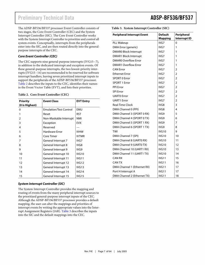
The ADSP-BF536/BF537 processor Event Controller consists of two stages, the Core Event Controller (CEC) and the System Interrupt Controller (SIC). The Core Event Controller works with the System Interrupt Controller to prioritize and control all system events. Conceptually, interrupts from the peripherals enter into the SIC, and are then routed directly into the general-purpose interrupts of the CEC.
Core Event Controller (CEC)
The CEC supports nine general-purpose interrupts (IVG15–7), in addition to the dedicated interrupt and exception events. Of these general-purpose interrupts, the two lowest-priority inter-rupts (IVG15–14) are recommended to be reserved for software interrupt handlers, leaving seven prioritized interrupt inputs to support the peripherals of the ADSP-BF536/BF537 processor. Table 2 describes the inputs to the CEC, identifies their names in the Event Vector Table (EVT), and lists their priorities.
System Interrupt Controller (SIC)
The System Interrupt Controller provides the mapping and routing of events from the many peripheral interrupt sources to the prioritized general-purpose interrupt inputs of the CEC. Although the ADSP-BF536/BF537 processor provides a default mapping, the user can alter the mappings and priorities of interrupt events by writing the appropriate values into the Inter-rupt Assignment Registers (IAR). Table 3 describes the inputs into the SIC and the default mappings into the CEC.
Table 2. Core Event Controller (CEC)
Priority(0 is Highest)
Event Class EVT Entry
0 Emulation/Test Control EMU
1 Reset RST
2 Non-Maskable Interrupt NMI
3 Exception EVX
4 Reserved —
5 Hardware Error IVHW
6 Core Timer IVTMR
7 General Interrupt 7 IVG7
8 General Interrupt 8 IVG8
9 General Interrupt 9 IVG9
10 General Interrupt 10 IVG10
11 General Interrupt 11 IVG11
12 General Interrupt 12 IVG12
13 General Interrupt 13 IVG13
14 General Interrupt 14 IVG14
15 General Interrupt 15 IVG15
Table 3. System Interrupt Controller (SIC)
Peripheral Interrupt Event Default Mapping
Peripheral Interrupt ID
PLL Wakeup IVG7 0
DMA Error (generic) IVG7 1
DMAR0 Block Interrupt IVG7 1
DMAR1 Block Interrupt IVG7 1
DMAR0 Overflow Error IVG7 1
DMAR1 Overflow Error IVG7 1
CAN Error IVG7 2
Ethernet Error IVG7 2
SPORT 0 Error IVG7 2
SPORT 1 Error IVG7 2
PPI Error IVG7 2
SPI Error IVG7 2
UART0 Error IVG7 2
UART1 Error IVG7 2
Real-Time Clock IVG8 3
DMA Channel 0 (PPI) IVG8 4
DMA Channel 3 (SPORT 0 RX) IVG9 5
DMA Channel 4 (SPORT 0 TX) IVG9 6
DMA Channel 5 (SPORT 1 RX) IVG9 7
DMA Channel 6 (SPORT 1 TX) IVG9 8
TWI IVG10 9
DMA Channel 7 (SPI) IVG10 10
DMA Channel 8 (UART0 RX) IVG10 11
DMA Channel 9 (UART0 TX) IVG10 12
DMA Channel 10 (UART1 RX) IVG10 13
DMA Channel 11 (UART1 TX) IVG10 14
CAN RX IVG11 15
CAN TX IVG11 16
DMA Channel 1 (Ethernet RX) IVG11 17
Port H Interrupt A IVG11 17
DMA Channel 2 (Ethernet TX) IVG11 18
Rev. PrE | Page 8 of 64 | July 2005
ADSP-BF536/BF537 Preliminary Technical Data
Event Control
The ADSP-BF536/BF537 processor provides the user with a very flexible mechanism to control the processing of events. In the CEC, three registers are used to coordinate and control events. Each register is 16 bits wide:
• CEC Interrupt Latch Register (ILAT) – The ILAT register indicates when events have been latched. The appropriate bit is set when the processor has latched the event and cleared when the event has been accepted into the system. This register is updated automatically by the controller, but it may be written only when its corresponding IMASK bit is cleared.
• CEC Interrupt Mask Register (IMASK) – The IMASK reg-ister controls the masking and unmasking of individual events. When a bit is set in the IMASK register, that event is unmasked and will be processed by the CEC when asserted. A cleared bit in the IMASK register masks the event, pre-venting the processor from servicing the event even though the event may be latched in the ILAT register. This register may be read or written while in supervisor mode. (Note that general-purpose interrupts can be globally enabled and disabled with the STI and CLI instructions, respectively.)
• CEC Interrupt Pending Register (IPEND) – The IPEND register keeps track of all nested events. A set bit in the IPEND register indicates the event is currently active or nested at some level. This register is updated automatically by the controller but may be read while in supervisor mode.
The SIC allows further control of event processing by providing three 32-bit interrupt control and status registers. Each register contains a bit corresponding to each of the peripheral interrupt events shown in Table 3 on Page 7.
• SIC Interrupt Mask Register (SIC_IMASK)– This register controls the masking and unmasking of each peripheral interrupt event. When a bit is set in the register, that peripheral event is unmasked and will be processed by the system when asserted. A cleared bit in the register masks the peripheral event, preventing the processor from servic-ing the event.
• SIC Interrupt Status Register (SIC_ISR) – As multiple peripherals can be mapped to a single event, this register allows the software to determine which peripheral event source triggered the interrupt. A set bit indicates the peripheral is asserting the interrupt, and a cleared bit indi-cates the peripheral is not asserting the event.
• SIC Interrupt Wakeup Enable Register (SIC_IWR) – By enabling the corresponding bit in this register, a peripheral can be configured to wake up the processor, should the core be idled when the event is generated. (For more infor-mation, see Dynamic Power Management on Page 13.)
Because multiple interrupt sources can map to a single general-purpose interrupt, multiple pulse assertions can occur simulta-neously, before or during interrupt processing for an interrupt event already detected on this interrupt input. The IPEND reg-ister contents are monitored by the SIC as the interrupt acknowledgement.The appropriate ILAT register bit is set when an interrupt rising edge is detected (detection requires two core clock cycles). The bit is cleared when the respective IPEND register bit is set. The IPEND bit indicates that the event has entered into the proces-sor pipeline. At this point the CEC will recognize and queue the next rising edge event on the corresponding event input. The minimum latency from the rising edge transition of the general-purpose interrupt to the IPEND output asserted is three core clock cycles; however, the latency can be much higher, depend-ing on the activity within and the state of the processor.
DMA CONTROLLERS
The ADSP-BF536/BF537 processor has multiple, independent DMA controllers that support automated data transfers with minimal overhead for the processor core. DMA transfers can occur between the ADSP-BF536/BF537 processor's internal memories and any of its DMA-capable peripherals. Addition-ally, DMA transfers can be accomplished between any of the DMA-capable peripherals and external devices connected to the external memory interfaces, including the SDRAM controller and the asynchronous memory controller. DMA-capable peripherals include the Ethernet MAC, SPORTs, SPI port, UARTs, and PPI. Each individual DMA-capable peripheral has at least one dedicated DMA channel.The ADSP-BF536/BF537 processor DMA controller supports both 1-dimensional (1D) and 2-dimensional (2D) DMA trans-fers. DMA transfer initialization can be implemented from registers or from sets of parameters called descriptor blocks.
Port H Interrupt B IVG11 18
Timer 0 IVG12 19
Timer 1 IVG12 20
Timer 2 IVG12 21
Timer 3 IVG12 22
Timer 4 IVG12 23
Timer 5 IVG12 24
Timer 6 IVG12 25
Timer 7 IVG12 26
Port F, G Interrupt A IVG12 27
Port G Interrupt B IVG12 28
DMA Channels 12 and 13 (Memory DMA Stream 0)
IVG13 29
DMA Channels 14 and 15(Memory DMA Stream 1)
IVG13 30
Software Watchdog Timer IVG13 31
Port F Interrupt B IVG13 31
Table 3. System Interrupt Controller (SIC) (Continued)
Peripheral Interrupt Event Default Mapping
Peripheral Interrupt ID

ADSP-BF536/BF537Preliminary Technical Data
Rev. PrE | Page 9 of 64 | July 2005
The 2D DMA capability supports arbitrary row and column sizes up to 64K elements by 64K elements, and arbitrary row and column step sizes up to ±32K elements. Furthermore, the column step size can be less than the row step size, allowing implementation of interleaved data streams. This feature is especially useful in video applications where data can be de-interleaved on the fly.Examples of DMA types supported by the ADSP-BF536/BF537 processor DMA controller include:
• A single, linear buffer that stops upon completion• A circular, auto-refreshing buffer that interrupts on each
full or fractionally full buffer• 1-D or 2-D DMA using a linked list of descriptors• 2-D DMA using an array of descriptors, specifying only the
base DMA address within a common pageIn addition to the dedicated peripheral DMA channels, there are two memory DMA channels provided for transfers between the various memories of the ADSP-BF536/BF537 processor system. This enables transfers of blocks of data between any of the memories—including external SDRAM, ROM, SRAM, and flash memory—with minimal processor intervention. Memory DMA transfers can be controlled by a very flexible descriptor-based methodology or by a standard register-based autobuffer mechanism.The ADSP-BF536/BF537 processors also include an external DMA controller capability via dual external DMA request pins when used in conjunction with the External Bus Interface Unit (EBIU). This functionality can be used when a high speed inter-face is required for external FIFOs and high bandwidth communications peripherals such as USB 2.0. It allows control of the number of data transfers for memDMA. The number of transfers per edge is programmable. This feature can be pro-grammed to allow memDMA to have an increased priority on the external bus relative to the core.
REAL-TIME CLOCK
The ADSP-BF536/BF537 processor Real-Time Clock (RTC) provides a robust set of digital watch features, including current time, stopwatch, and alarm. The RTC is clocked by a 32.768 KHz crystal external to the ADSP-BF536/BF537 proces-sor. The RTC peripheral has dedicated power supply pins so that it can remain powered up and clocked even when the rest of the processor is in a low-power state. The RTC provides several programmable interrupt options, including interrupt per sec-ond, minute, hour, or day clock ticks, interrupt on programmable stopwatch countdown, or interrupt at a pro-grammed alarm time.The 32.768 KHz input clock frequency is divided down to a 1 Hz signal by a prescaler. The counter function of the timer consists of four counters: a 60-second counter, a 60-minute counter, a 24-hour counter, and an 32,768-day counter.
When enabled, the alarm function generates an interrupt when the output of the timer matches the programmed value in the alarm control register. There are two alarms: The first alarm is for a time of day. The second alarm is for a day and time of that day.The stopwatch function counts down from a programmed value, with one-second resolution. When the stopwatch is enabled and the counter underflows, an interrupt is generated.Like the other peripherals, the RTC can wake up the ADSP-BF536/BF537 processor from Sleep mode upon generation of any RTC wakeup event. Additionally, an RTC wakeup event can wake up the ADSP-BF536/BF537 processor from Deep Sleep mode, and wake up the on-chip internal voltage regulator from the Hibernate operating mode.Connect RTC pins RTXI and RTXO with external components as shown in Figure 5.
WATCHDOG TIMER
The ADSP-BF536/BF537 processor includes a 32-bit timer that can be used to implement a software watchdog function. A soft-ware watchdog can improve system availability by forcing the processor to a known state through generation of a hardware reset, non-maskable interrupt (NMI), or general-purpose inter-rupt, if the timer expires before being reset by software. The programmer initializes the count value of the timer, enables the appropriate interrupt, then enables the timer. Thereafter, the software must reload the counter before it counts to zero from the programmed value. This protects the system from remain-ing in an unknown state where software, which would normally reset the timer, has stopped running due to an external noise condition or software error.If configured to generate a hardware reset, the watchdog timer resets both the core and the ADSP-BF536/BF537 processor peripherals. After a reset, software can determine if the watch-dog was the source of the hardware reset by interrogating a status bit in the watchdog timer control register.
Figure 5. External Components for RTC
RTXO
C1 C2
X1
SUGGESTED COMPONENTS:ECLIPTEK EC38J (THROUGH-HOLE PACKAGE)EPSON MC405 12 PF LOAD (SURFACE MOUNT PACKAGE)C1 = 22 PFC2 = 22 PFR1 = 10 M
NOTE: C1 AND C2 ARE SPECIFIC TO CRYSTAL SPECIFIED FOR X1.CONTACT CRYSTAL MANUFACTURER FOR DETAILS. C1 AND C2SPECIFICATIONS ASSUME BOARD TRACE CAPACITANCE OF 3 PF.
RTXI
R1
�
Rev. PrE | Page 10 of 64 | July 2005
ADSP-BF536/BF537 Preliminary Technical Data
The timer is clocked by the system clock (SCLK), at a maximum frequency of fSCLK.
TIMERS
There are nine general-purpose programmable timer units in the ADSP-BF536/BF537 processor. Eight timers have an exter-nal pin that can be configured either as a Pulse Width Modulator (PWM) or timer output, as an input to clock the timer, or as a mechanism for measuring pulse widths and peri-ods of external events. These timers can be synchronized to an external clock input to the several other associated PF pins, an external clock input to the PPI_CLK input pin, or to the internal SCLK.The timer units can be used in conjunction with the two UARTs and the CAN controller to measure the width of the pulses in the data stream to provide a software auto-baud detect function for the respective serial channels. The timers can generate interrupts to the processor core provid-ing periodic events for synchronization, either to the system clock or to a count of external signals.In addition to the eight general-purpose programmable timers, a ninth timer is also provided. This extra timer is clocked by the internal processor clock and is typically used as a system tick clock for generation of operating system periodic interrupts.
SERIAL PORTS (SPORTS)
The ADSP-BF536/BF537 processor incorporates two dual-channel synchronous serial ports (SPORT0 and SPORT1) for serial and multiprocessor communications. The SPORTs sup-port the following features:
• I2S capable operation.• Bidirectional operation – Each SPORT has two sets of inde-
pendent transmit and receive pins, enabling eight channels of I2S stereo audio.
• Buffered (8-deep) transmit and receive ports – Each port has a data register for transferring data words to and from other processor components and shift registers for shifting data in and out of the data registers.
• Clocking – Each transmit and receive port can either use an external serial clock or generate its own, in frequencies ranging from (fSCLK/131,070) Hz to (fSCLK/2) Hz.
• Word length – Each SPORT supports serial data words from 3 to 32 bits in length, transferred most-significant-bit first or least-significant-bit first.
• Framing – Each transmit and receive port can run with or without frame sync signals for each data word. Frame sync signals can be generated internally or externally, active high or low, and with either of two pulsewidths and early or late frame sync.
• Companding in hardware – Each SPORT can perform A-law or µ-law companding according to ITU recommen-dation G.711. Companding can be selected on the transmit and/or receive channel of the SPORT without additional latencies.
• DMA operations with single-cycle overhead – Each SPORT can automatically receive and transmit multiple buffers of memory data. The processor can link or chain sequences of DMA transfers between a SPORT and memory.
• Interrupts – Each transmit and receive port generates an interrupt upon completing the transfer of a data word or after transferring an entire data buffer or buffers through DMA.
• Multichannel capability – Each SPORT supports 128 chan-nels out of a 1024-channel window and is compatible with the H.100, H.110, MVIP-90, and HMVIP standards.
SERIAL PERIPHERAL INTERFACE (SPI) PORT
The ADSP-BF536/BF537 processor has an SPI-compatible port that enables the processor to communicate with multiple SPI-compatible devices. The SPI interface uses three pins for transferring data: two data pins (Master Output-Slave Input, MOSI, and Master Input-Slave Output, MISO) and a clock pin (Serial Clock, SCK). An SPI chip select input pin (SPISS) lets other SPI devices select the processor, and seven SPI chip select output pins (SPISEL7–1) let the processor select other SPI devices. The SPI select pins are reconfigured Programmable Flag pins. Using these pins, the SPI port provides a full-duplex, synchronous serial interface, which supports both master/slave modes and multimaster environments. The SPI port’s baud rate and clock phase/polarities are pro-grammable, and it has an integrated DMA controller, configurable to support transmit or receive data streams. The SPI’s DMA controller can only service unidirectional accesses at any given time.The SPI port’s clock rate is calculated as:
Where the 16-bit SPI_Baud register contains a value of 2 to 65,535.During transfers, the SPI port simultaneously transmits and receives by serially shifting data in and out on its two serial data lines. The serial clock line synchronizes the shifting and sam-pling of data on the two serial data lines.
SPI Clock RatefSCLK
2 SPI_Baud×---------------------------------=

ADSP-BF536/BF537Preliminary Technical Data
Rev. PrE | Page 11 of 64 | July 2005
UART PORTS (UARTS)
The ADSP-BF536/BF537 processor provides two full-duplex Universal Asynchronous Receiver/Transmitter (UART) ports, which are fully compatible with PC-standard UARTs. Each UART port provides a simplified UART interface to other peripherals or hosts, supporting full-duplex, DMA-supported, asynchronous transfers of serial data. A UART port includes support for 5 to 8 data bits, 1 or 2 stop bits, and none, even, or odd parity. Each UART port supports two modes of operation:
• PIO (Programmed I/O) – The processor sends or receives data by writing or reading I/O-mapped UART registers. The data is double-buffered on both transmit and receive.
• DMA (Direct Memory Access) – The DMA controller transfers both transmit and receive data. This reduces the number and frequency of interrupts required to transfer data to and from memory. The UART has two dedicated DMA channels, one for transmit and one for receive. These DMA channels have lower default priority than most DMA channels because of their relatively low service rates.
Each UART port's baud rate, serial data format, error code gen-eration and status, and interrupts are programmable:
• Supporting bit rates ranging from (fSCLK/ 1,048,576) to (fSCLK/16) bits per second.
• Supporting data formats from 7 to12 bits per frame.• Both transmit and receive operations can be configured to
generate maskable interrupts to the processor.The UART port’s clock rate is calculated as:
Where the 16-bit UART_Divisor comes from the DLH register (most significant 8 bits) and DLL register (least significant 8 bits).In conjunction with the general-purpose timer functions, auto-baud detection is supported. The capabilities of the UARTs are further extended with sup-port for the Infrared Data Association (IrDA®) Serial Infrared Physical Layer Link Specification (SIR) protocol.
CONTROLLER AREA NETWORK (CAN)
The ADSP-BF536/BF537 processor offers a CAN controller that is a communication controller implementing the Controller Area Network (CAN) 2.0B (active) protocol. This protocol is an asynchronous communications protocol used in both industrial and automotive control systems. The CAN protocol is well suited for control applications due to its capability to communi-cate reliably over a network since the protocol incorporates CRC checking message error tracking, and fault node confinement.
The ADSP-BF536/BF537 CAN controller offers the following features:
• 32 mailboxes (8 receive only, 8 transmit only, 16 config-urable for receive or transmit).
• Dedicated acceptance masks for each mailbox.• Additional data filtering on first two bytes.• Support for both the standard (11-bit) and extended (29-
bit) identifier (ID) message formats.• Support for remote frames.• Active or passive network support.• CAN wakeup from Hibernation Mode (lowest static power
consumption mode).• Interrupts, including: TX Complete, RX Complete, Error,
Global.The electrical characteristics of each network connection are very demanding so the CAN interface is typically divided into two parts: a controller and a transceiver. This allows a single controller to support different drivers and CAN networks. The ADSP-BF536/BF537 CAN module represents only the control-ler part of the interface. The controller interface supports connection to 3.3V high-speed, fault-tolerant, single-wire transceivers.
TWI CONTROLLER INTERFACE
The ADSP-BF536/BF537 processor includes a Two Wire Inter-face (TWI) module for providing a simple exchange method of control data between multiple devices. The TWI is compatible with the widely used I2C bus standard. The TWI module offers the capabilities of simultaneous Master and Slave operation, support for both 7-bit addressing and multimedia data arbitra-tion. The TWI interface utilizes two pins for transferring clock (SCL) and data (SDA) and supports the protocol at speeds up to 400k bits/sec. The TWI interface pins are compatible with 5 V logic levels.Additionally, the ADSP-BF536/BF537 processor’s TWI module is fully compatible with Serial Camera Control Bus (SCCB) functionality for easier control of various CMOS camera sensor devices.
10/100 ETHERNET MAC
The ADSP-BF536/BF537 processor offers the capability to directly connect to a network by way of an embedded Fast Ethernet Medium Access Controller (MAC) that supports both 10-BaseT (10Mbits/sec) and 100-BaseT (100Mbits/sec) opera-tion. The 10/100 Ethernet MAC peripheral on the ADSP-BF536/BF537 is fully compliant to the IEEE 802.3-2002 stan-dard and it provides programmable features designed to minimize supervision, bus utilization, or message processing by the rest of the processor system.Some standard features are:
• Support of MII and RMII protocols for external PHYs.• Full Duplex and Half Duplex modes.
UART Clock RatefSCLK
16 UART_Divisor×------------------------------------------------=

Rev. PrE | Page 12 of 64 | July 2005
ADSP-BF536/BF537 Preliminary Technical Data
• Data framing and encapsulation: generation and detection of preamble, length padding, and FCS.
• Media access management (in Half-Duplex operation): col-lision and contention handling, including control of retransmission of collision frames and of back-off timing.
• Flow control (in Full-Duplex operation): generation and detection of PAUSE frames.
• Station management: generation of MDC/MDIO frames for read-write access to PHY registers.
• SCLK operating range down to 25MHz (Active and Sleep operating modes).
• Internal loopback from TX to RX.Some advanced features are:
• Buffered crystal output to external PHY for support of a single crystal system.
• Automatic checksum computation of IP header and IP payload fields of RX frames.
• Independent 32-bit descriptor-driven RX and TX DMA channels.
• Frame status delivery to memory via DMA, including frame completion semaphores, for efficient buffer queue management in software.
• TX DMA support for separate descriptors for MAC header and payload to eliminate buffer copy operations.
• Convenient frame alignment modes support even 32-bit alignment of encapsulated RX or TX IP packet data in memory after the 14-byte MAC header.
• Programmable Ethernet event interrupt supports any com-bination of:
• Any selected RX or TX frame status conditions.• PHY interrupt condition.• Wakeup frame detected.• Any selected MAC management counter(s) at half-
full.• DMA descriptor error.
• 47 MAC management statistics counters with selectable clear-on-read behavior and programmable interrupts on half maximum value.
• Programmable RX address filters, including a 64-bin address hash table for multicast and/or unicast frames, and programmable filter modes for broadcast, multicast, uni-cast, control, and damaged frames.
• Advanced power management supporting unattended transfer of RX and TX frames and status to/from external memory via DMA during low-power Sleep mode.
• System wakeup from Sleep operating mode upon magic packet or any of four user-definable wakeup frame filters.
• Support for 802.3Q tagged VLAN frames.
• Programmable MDC clock rate and preamble suppression.• In RMII operation, 7 unused pins may be configured as
GPIO pins for other purposes.
PORTS
Because of the rich set of peripherals, the ADSP-BF536/BF537 processor groups the many peripheral signals to four ports—Port F, Port G, Port H, and Port J. Most of the associated pins are shared by multiple signals. The ports function as multiplexer controls. Eight of the pins (Port F7–0) offer high source/high sink current capabilities.
General-Purpose I/O (GPIO)
The ADSP-BF536/BF537 processor has 48 bi-directional, gen-eral-purpose I/O (GPIO) pins allocated across three separate GPIO modules—PORTFIO, PORTGIO, and PORTHIO, asso-ciated with Port F, Port G, and Port H, respectively. Port J does not provide GPIO functionality. Each GPIO-capable pin shares functionality with other ADSP-BF536/BF537 processor periph-erals via a multiplexing scheme; however, the GPIO functionality is the default state of the device upon power-up. Neither GPIO output or input drivers are active by default. Each general-purpose port pin can be individually controlled by manipulation of the port control, status, and interrupt registers:
• GPIO Direction Control Register – Specifies the direction of each individual GPIO pin as input or output.
• GPIO Control and Status Registers – The ADSP-BF536/BF537 processor employs a “write one to modify” mechanism that allows any combination of individual GPIO pins to be modified in a single instruction, without affecting the level of any other GPIO pins. Four control registers are provided. One register is written in order to set pin values, one register is written in order to clear pin val-ues, one register is written in order to toggle pin values, and one register is written in order to specify a pin value. Read-ing the GPIO status register allows software to interrogate the sense of the pins.
• GPIO Interrupt Mask Registers – The two GPIO Interrupt Mask registers allow each individual GPIO pin to function as an interrupt to the processor. Similar to the two GPIO Control Registers that are used to set and clear individual pin values, one GPIO Interrupt Mask Register sets bits to enable interrupt function, and the other GPIO Interrupt Mask register clears bits to disable interrupt function. GPIO pins defined as inputs can be configured to generate hardware interrupts, while output pins can be triggered by software interrupts.
• GPIO Interrupt Sensitivity Registers – The two GPIO Interrupt Sensitivity Registers specify whether individual pins are level- or edge-sensitive and specify—if edge-sensi-tive—whether just the rising edge or both the rising and falling edges of the signal are significant. One register selects the type of sensitivity, and one register selects which edges are significant for edge-sensitivity.
ADSP-BF536/BF537Preliminary Technical Data
Rev. PrE | Page 13 of 64 | July 2005
PARALLEL PERIPHERAL INTERFACE (PPI)
The ADSP-BF536/BF537 processor provides a Parallel Periph-eral Interface (PPI) that can connect directly to parallel A/D and D/A converters, ITU-R-601/656 video encoders and decoders, and other general-purpose peripherals. The PPI consists of a dedicated input clock pin, up to 3 frame synchronization pins, and up to 16 data pins.In ITU-R-656 modes, the PPI receives and parses a data stream of 8-bit or 10-bit data elements. On-chip decode of embedded preamble control and synchronization information is supported.Three distinct ITU-R-656 modes are supported:
• Active Video Only Mode—The PPI does not read in any data between the End of Active Video (EAV) and Start of Active Video (SAV) preamble symbols, or any data present during the vertical blanking intervals. In this mode, the control byte sequences are not stored to memory; they are filtered by the PPI.
• Vertical Blanking Only Mode—The PPI only transfers Ver-tical Blanking Interval (VBI) data, as well as horizontal blanking information and control byte sequences on VBI lines.
• Entire Field Mode—The entire incoming bitstream is read in through the PPI. This includes active video, control pre-amble sequences, and ancillary data that may be embedded in horizontal and vertical blanking intervals.
Though not explicitly supported, ITU-R-656 output functional-ity can be achieved by setting up the entire frame structure (including active video, blanking, and control information) in memory and streaming the data out the PPI in a frame sync-less mode. The processor’s 2D DMA features facilitate this transfer by allowing the static frame buffer (blanking and control codes) to be placed in memory once, and simply updating the active video information on a per-frame basis.The general-purpose modes of the PPI are intended to suit a wide variety of data capture and transmission applications. The modes are divided into four main categories, each allowing up to 16 bits of data transfer per PPI_CLK cycle:
• Data Receive with Internally Generated Frame Syncs.• Data Receive with Externally Generated Frame Syncs.• Data Transmit with Internally Generated Frame Syncs• Data Transmit with Externally Generated Frame Syncs
These modes support ADC/DAC connections, as well as video communication with hardware signalling. Many of the modes support more than one level of frame synchronization. If desired, a programmable delay can be inserted between asser-tion of a frame sync and reception/transmission of data.
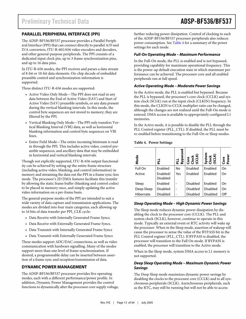
DYNAMIC POWER MANAGEMENT
The ADSP-BF536/BF537 processor provides five operating modes, each with a different performance/power profile. In addition, Dynamic Power Management provides the control functions to dynamically alter the processor core supply voltage,
further reducing power dissipation. Control of clocking to each of the ADSP-BF536/BF537 processor peripherals also reduces power consumption. See Table 4 for a summary of the power settings for each mode.
Full-On Operating Mode – Maximum Performance
In the Full-On mode, the PLL is enabled and is not bypassed, providing capability for maximum operational frequency. This is the power-up default execution state in which maximum per-formance can be achieved. The processor core and all enabled peripherals run at full speed.
Active Operating Mode – Moderate Power Savings
In the Active mode, the PLL is enabled but bypassed. Because the PLL is bypassed, the processor’s core clock (CCLK) and sys-tem clock (SCLK) run at the input clock (CLKIN) frequency. In this mode, the CLKIN to CCLK multiplier ratio can be changed, although the changes are not realized until the Full-On mode is entered. DMA access is available to appropriately configured L1 memories.In the Active mode, it is possible to disable the PLL through the PLL Control register (PLL_CTL). If disabled, the PLL must be re-enabled before transitioning to the Full-On or Sleep modes.
Sleep Operating Mode – High Dynamic Power Savings
The Sleep mode reduces dynamic power dissipation by dis-abling the clock to the processor core (CCLK). The PLL and system clock (SCLK), however, continue to operate in this mode. Typically an external event or RTC activity will wake up the processor. When in the Sleep mode, assertion of wakeup will cause the processor to sense the value of the BYPASS bit in the PLL Control register (PLL_CTL). If BYPASS is disabled, the processor will transition to the Full On mode. If BYPASS is enabled, the processor will transition to the Active mode. When in the Sleep mode, system DMA access to L1 memory is not supported.
Deep Sleep Operating Mode – Maximum Dynamic Power Savings
The Deep Sleep mode maximizes dynamic power savings by disabling the clocks to the processor core (CCLK) and to all syn-chronous peripherals (SCLK). Asynchronous peripherals, such as the RTC, may still be running but will not be able to access
Table 4. Power Settings M
od
e
PLL
PLL
Byp
asse
d
Co
reC
lock
(CC
LK)
Syst
emC
lock
(SC
LK)
Co
rePo
wer
Full On Enabled No Enabled Enabled On
Active Enabled/ Disabled
Yes Enabled Enabled On
Sleep Enabled - Disabled Enabled On
Deep Sleep Disabled - Disabled Disabled On
Hibernate Disabled - Disabled Disabled Off
Rev. PrE | Page 14 of 64 | July 2005
ADSP-BF536/BF537 Preliminary Technical Data
internal resources or external memory. This powered-down mode can only be exited by assertion of the reset interrupt (RESET) or by an asynchronous interrupt generated by the RTC. When in Deep Sleep mode, an RTC asynchronous inter-rupt causes the processor to transition to the Active mode. Assertion of RESET while in Deep Sleep mode causes the pro-cessor to transition to the Full On mode.
Hibernate Operating Mode – Maximum Static Power Savings
The hibernate mode maximizes static power savings by dis-abling the voltage and clocks to the processor core (CCLK) and to all the synchronous peripherals (SCLK). The internal voltage regulator for the processor can be shut off by writing b#00 to the FREQ bits of the VR_CTL register. This disables both CCLK and SCLK. Furthermore, it sets the internal power supply volt-age (VDDINT) to 0V to provide the greatest power savings mode. Any critical information stored internally (memory contents, register contents, etc.) must be written to a non-volatile storage device prior to removing power if the processor state is to be preserved.Since VDDEXT is still supplied in this mode, all of the external pins tri-state, unless otherwise specified. This allows other devices that may be connected to the processor to have power still applied without drawing unwanted current.The internal supply regulator can be woken up by CAN or by Ethernet. It can also be woken up by a Real-Time Clock wakeup event or by asserting the RESET pin, both of which initiate the hardware reset sequence.With the exception of the VR_CTL and the RTC registers, all internal registers and memories lose their content in hibernate state. State variables may be held in external SRAM or SDRAM. The CKELOW bit in the VR_CTL register controls whether SDRAM operates in self-refresh mode to retain its content while the processor is in reset.
Power Savings
As shown in Table 5, the ADSP-BF536/BF537 processor sup-ports three different power domains. The use of multiple power domains maximizes flexibility, while maintaining compliance with industry standards and conventions. By isolating the inter-nal logic of the ADSP-BF536/BF537 processor into its own power domain, separate from the RTC and other I/O, the pro-cessor can take advantage of Dynamic Power Management, without affecting the RTC or other I/O devices. There are no sequencing requirements for the various power domains.
The power dissipated by a processor is largely a function of the clock frequency of the processor and the square of the operating voltage. For example, reducing the clock frequency by 25%
results in a 25% reduction in power dissipation, while reducing the voltage by 25% reduces power dissipation by more than 40%. Further, these power savings are additive, in that if the clock frequency and supply voltage are both reduced, the power savings can be dramatic.The Dynamic Power Management feature of the ADSP-BF536/BF537 processor allows both the processor’s input volt-age (VDDINT) and clock frequency (fCCLK) to be dynamically controlled. As explained above, the savings in power dissipation can be modeled by the following equations:
where the variables in the equations are:• fCCLKNOM is the nominal core clock frequency • fCCLKRED is the reduced core clock frequency• VDDINTNOM is the nominal internal supply voltage • VDDINTRED is the reduced internal supply voltage• TNOM is the duration running at fCCLKNOM
• TRED is the duration running at fCCLKRED
VOLTAGE REGULATION
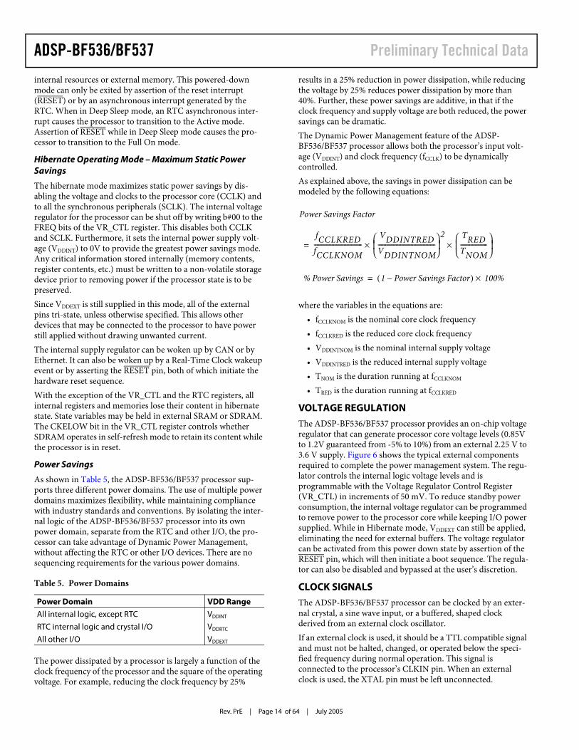
The ADSP-BF536/BF537 processor provides an on-chip voltage regulator that can generate processor core voltage levels (0.85V to 1.2V guaranteed from -5% to 10%) from an external 2.25 V to 3.6 V supply. Figure 6 shows the typical external components required to complete the power management system. The regu-lator controls the internal logic voltage levels and is programmable with the Voltage Regulator Control Register (VR_CTL) in increments of 50 mV. To reduce standby power consumption, the internal voltage regulator can be programmed to remove power to the processor core while keeping I/O power supplied. While in Hibernate mode, VDDEXT can still be applied, eliminating the need for external buffers. The voltage regulator can be activated from this power down state by assertion of the RESET pin, which will then initiate a boot sequence. The regula-tor can also be disabled and bypassed at the user’s discretion.
CLOCK SIGNALS
The ADSP-BF536/BF537 processor can be clocked by an exter-nal crystal, a sine wave input, or a buffered, shaped clock derived from an external clock oscillator. If an external clock is used, it should be a TTL compatible signal and must not be halted, changed, or operated below the speci-fied frequency during normal operation. This signal is connected to the processor’s CLKIN pin. When an external clock is used, the XTAL pin must be left unconnected.
Table 5. Power Domains
Power Domain VDD Range
All internal logic, except RTC VDDINT
RTC internal logic and crystal I/O VDDRTC
All other I/O VDDEXT
Power Savings Factor
fCCLKREDfCCLKNOM--------------------------------
VDDINTREDVDDINTNOM--------------------------------------
2
×TREDTNOM------------------
×
=
% Power Savings 1 Power Savings Factor–( ) 100%×=
ADSP-BF536/BF537Preliminary Technical Data
Rev. PrE | Page 15 of 64 | July 2005
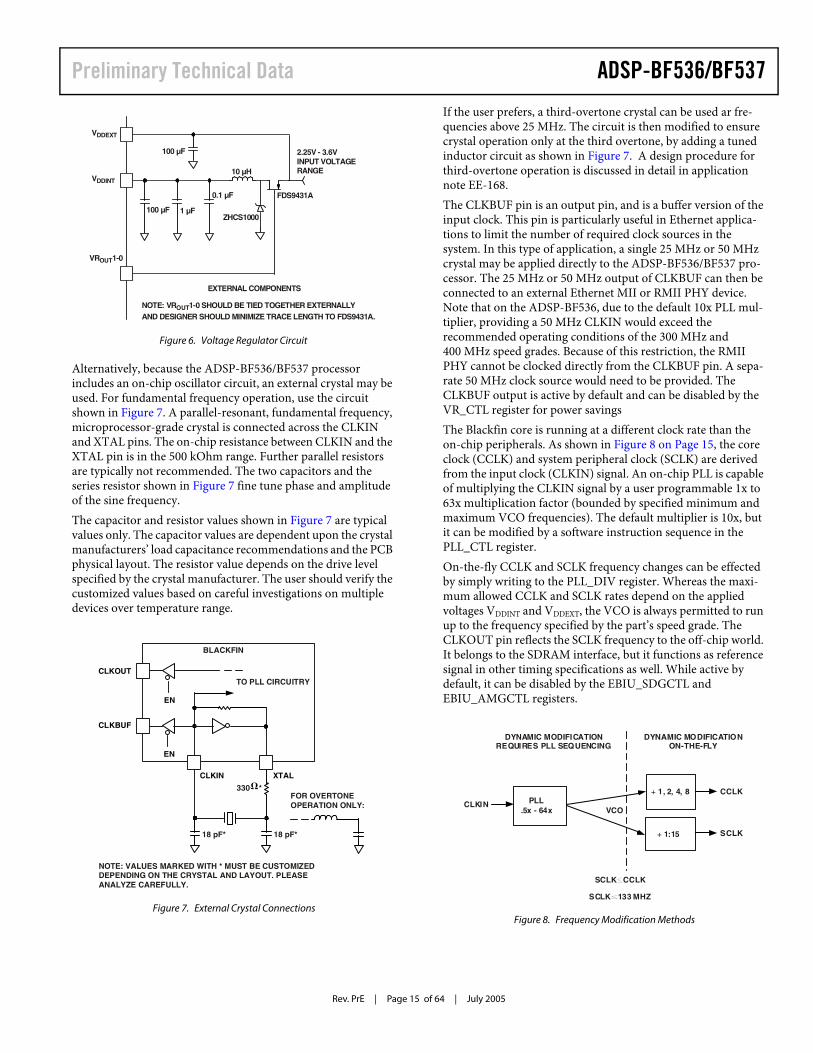
Alternatively, because the ADSP-BF536/BF537 processor includes an on-chip oscillator circuit, an external crystal may be used. For fundamental frequency operation, use the circuit shown in Figure 7. A parallel-resonant, fundamental frequency, microprocessor-grade crystal is connected across the CLKIN and XTAL pins. The on-chip resistance between CLKIN and the XTAL pin is in the 500 kOhm range. Further parallel resistors are typically not recommended. The two capacitors and the series resistor shown in Figure 7 fine tune phase and amplitude of the sine frequency. The capacitor and resistor values shown in Figure 7 are typical values only. The capacitor values are dependent upon the crystal manufacturers’ load capacitance recommendations and the PCB physical layout. The resistor value depends on the drive level specified by the crystal manufacturer. The user should verify the customized values based on careful investigations on multiple devices over temperature range.
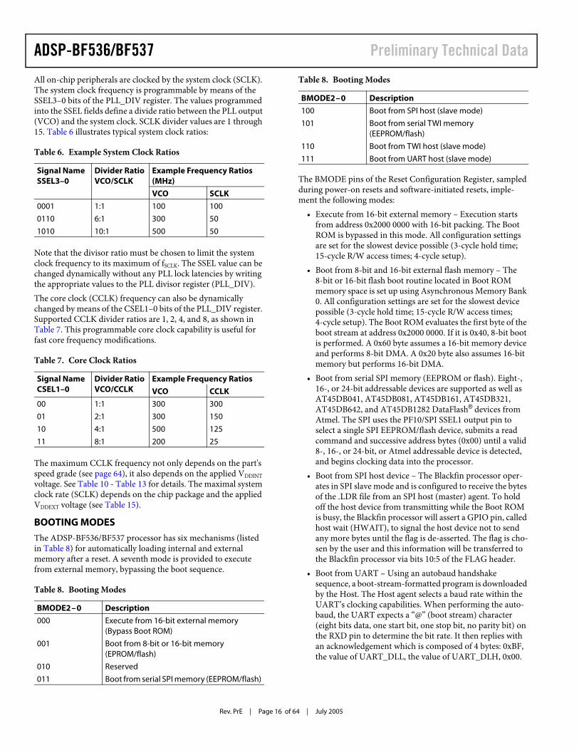
If the user prefers, a third-overtone crystal can be used ar fre-quencies above 25 MHz. The circuit is then modified to ensure crystal operation only at the third overtone, by adding a tuned inductor circuit as shown in Figure 7. A design procedure for third-overtone operation is discussed in detail in application note EE-168.The CLKBUF pin is an output pin, and is a buffer version of the input clock. This pin is particularly useful in Ethernet applica-tions to limit the number of required clock sources in the system. In this type of application, a single 25 MHz or 50 MHz crystal may be applied directly to the ADSP-BF536/BF537 pro-cessor. The 25 MHz or 50 MHz output of CLKBUF can then be connected to an external Ethernet MII or RMII PHY device. Note that on the ADSP-BF536, due to the default 10x PLL mul-tiplier, providing a 50 MHz CLKIN would exceed the recommended operating conditions of the 300 MHz and 400 MHz speed grades. Because of this restriction, the RMII PHY cannot be clocked directly from the CLKBUF pin. A sepa-rate 50 MHz clock source would need to be provided. The CLKBUF output is active by default and can be disabled by the VR_CTL register for power savingsThe Blackfin core is running at a different clock rate than the on-chip peripherals. As shown in Figure 8 on Page 15, the core clock (CCLK) and system peripheral clock (SCLK) are derived from the input clock (CLKIN) signal. An on-chip PLL is capable of multiplying the CLKIN signal by a user programmable 1x to 63x multiplication factor (bounded by specified minimum and maximum VCO frequencies). The default multiplier is 10x, but it can be modified by a software instruction sequence in the PLL_CTL register. On-the-fly CCLK and SCLK frequency changes can be effected by simply writing to the PLL_DIV register. Whereas the maxi-mum allowed CCLK and SCLK rates depend on the applied voltages VDDINT and VDDEXT, the VCO is always permitted to run up to the frequency specified by the part’s speed grade. The CLKOUT pin reflects the SCLK frequency to the off-chip world. It belongs to the SDRAM interface, but it functions as reference signal in other timing specifications as well. While active by default, it can be disabled by the EBIU_SDGCTL and EBIU_AMGCTL registers.
Figure 6. Voltage Regulator Circuit
Figure 7. External Crystal Connections
VDDEXT
VDDINT
VROUT1-0
EXTERNAL COMPONENTS
2.25V - 3.6VINPUT VOLTAGERANGE
FDS9431A
ZHCS1000100 µF 1 µF
10 µH
0.1 µF
NOTE: VROUT1-0 SHOULD BE TIED TOGETHER EXTERNALLYAND DESIGNER SHOULD MINIMIZE TRACE LENGTH TO FDS9431A.
100 µF
CLKIN
CLKOUT
XTAL
EN
CLKBUF
TO PLL CIRCUITRY
FOR OVERTONEOPERATION ONLY:
NOTE: VALUES MARKED WITH * MUST BE CUSTOMIZEDDEPENDING ON THE CRYSTAL AND LAYOUT. PLEASEANALYZE CAREFULLY.
18 pF*
EN
18 pF*
330 *
BLACKFIN
�
Figure 8. Frequency Modification Methods
PLL.5x - 64x
+ 1:15
+ 1, 2, 4, 8
VCO
SCLK CCLK
SCLK 133 MHZ
CLKIN
DYNAMIC MODIFICATIONREQUIRES PLL SEQUENCING
DYNAMIC MODIFICATIONON-THE-FLY
CCLK
SCLK
Rev. PrE | Page 16 of 64 | July 2005
ADSP-BF536/BF537 Preliminary Technical Data
All on-chip peripherals are clocked by the system clock (SCLK). The system clock frequency is programmable by means of the SSEL3–0 bits of the PLL_DIV register. The values programmed into the SSEL fields define a divide ratio between the PLL output (VCO) and the system clock. SCLK divider values are 1 through 15. Table 6 illustrates typical system clock ratios:
Note that the divisor ratio must be chosen to limit the system clock frequency to its maximum of fSCLK. The SSEL value can be changed dynamically without any PLL lock latencies by writing the appropriate values to the PLL divisor register (PLL_DIV).The core clock (CCLK) frequency can also be dynamically changed by means of the CSEL1–0 bits of the PLL_DIV register. Supported CCLK divider ratios are 1, 2, 4, and 8, as shown in Table 7. This programmable core clock capability is useful for fast core frequency modifications.
The maximum CCLK frequency not only depends on the part's speed grade (see page 64), it also depends on the applied VDDINT voltage. See Table 10 - Table 13 for details. The maximal system clock rate (SCLK) depends on the chip package and the applied VDDEXT voltage (see Table 15).
BOOTING MODES
The ADSP-BF536/BF537 processor has six mechanisms (listed in Table 8) for automatically loading internal and external memory after a reset. A seventh mode is provided to execute from external memory, bypassing the boot sequence.
The BMODE pins of the Reset Configuration Register, sampled during power-on resets and software-initiated resets, imple-ment the following modes:
• Execute from 16-bit external memory – Execution starts from address 0x2000 0000 with 16-bit packing. The Boot ROM is bypassed in this mode. All configuration settings are set for the slowest device possible (3-cycle hold time; 15-cycle R/W access times; 4-cycle setup).
• Boot from 8-bit and 16-bit external flash memory – The 8-bit or 16-bit flash boot routine located in Boot ROM memory space is set up using Asynchronous Memory Bank 0. All configuration settings are set for the slowest device possible (3-cycle hold time; 15-cycle R/W access times; 4-cycle setup). The Boot ROM evaluates the first byte of the boot stream at address 0x2000 0000. If it is 0x40, 8-bit boot is performed. A 0x60 byte assumes a 16-bit memory device and performs 8-bit DMA. A 0x20 byte also assumes 16-bit memory but performs 16-bit DMA.
• Boot from serial SPI memory (EEPROM or flash). Eight-, 16-, or 24-bit addressable devices are supported as well as AT45DB041, AT45DB081, AT45DB161, AT45DB321, AT45DB642, and AT45DB1282 DataFlash® devices from Atmel. The SPI uses the PF10/SPI SSEL1 output pin to select a single SPI EEPROM/flash device, submits a read command and successive address bytes (0x00) until a valid 8-, 16-, or 24-bit, or Atmel addressable device is detected, and begins clocking data into the processor.
• Boot from SPI host device – The Blackfin processor oper-ates in SPI slave mode and is configured to receive the bytes of the .LDR file from an SPI host (master) agent. To hold off the host device from transmitting while the Boot ROM is busy, the Blackfin processor will assert a GPIO pin, called host wait (HWAIT), to signal the host device not to send any more bytes until the flag is de-asserted. The flag is cho-sen by the user and this information will be transferred to the Blackfin processor via bits 10:5 of the FLAG header.
• Boot from UART – Using an autobaud handshake sequence, a boot-stream-formatted program is downloaded by the Host. The Host agent selects a baud rate within the UART’s clocking capabilities. When performing the auto-baud, the UART expects a “@” (boot stream) character (eight bits data, one start bit, one stop bit, no parity bit) on the RXD pin to determine the bit rate. It then replies with an acknowledgement which is composed of 4 bytes: 0xBF, the value of UART_DLL, the value of UART_DLH, 0x00.
Table 6. Example System Clock Ratios
Signal Name SSEL3–0
Divider Ratio VCO/SCLK
Example Frequency Ratios (MHz)
VCO SCLK
0001 1:1 100 100
0110 6:1 300 50
1010 10:1 500 50
Table 7. Core Clock Ratios
Signal Name CSEL1–0
Divider Ratio VCO/CCLK
Example Frequency Ratios
VCO CCLK
00 1:1 300 300
01 2:1 300 150
10 4:1 500 125
11 8:1 200 25
Table 8. Booting Modes
BMODE2–0 Description
000 Execute from 16-bit external memory (Bypass Boot ROM)
001 Boot from 8-bit or 16-bit memory (EPROM/flash)
010 Reserved
011 Boot from serial SPI memory (EEPROM/flash)
100 Boot from SPI host (slave mode)
101 Boot from serial TWI memory (EEPROM/flash)
110 Boot from TWI host (slave mode)
111 Boot from UART host (slave mode)
Table 8. Booting Modes
BMODE2–0 Description
ADSP-BF536/BF537Preliminary Technical Data
Rev. PrE | Page 17 of 64 | July 2005
The Host can then download the boot stream. When the processor needs to hold off the Host, it de-asserts CTS. Therefore, the Host must monitor this signal.
• Boot from serial TWI memory (EEPROM/flash) – The Blackfin processor operates in master mode and selects the TWI slave with the unique id 0xA0. It submits successive read commands to the memory device starting at two byte internal address 0x0000 and begins clocking data into the processor. The TWI memory device should comply with Philips I2C Bus Specification version 2.1 and have the capa-bility to auto-increment its internal address counter such that the contents of the memory device can be read sequentially.
• Boot from TWI Host – The TWI Host agent selects the slave with the unique id 0x5F. The processor replies with an acknowledgement and the Host can then download the boot stream. The TWI Host agent should comply with Philips I2C Bus Specification version 2.1. An I2C multi-plexer can be used to select one processor at a time when booting multiple processors from a single TWI.
For each of the boot modes, a 10-byte header is first brought in from an external device. The header specifies the number of bytes to be transferred and the memory destination address. Multiple memory blocks may be loaded by any boot sequence. Once all blocks are loaded, program execution commences from the start of L1 instruction SRAM.In addition, bit 4 of the Reset Configuration Register can be set by application code to bypass the normal boot sequence during a software reset. For this case, the processor jumps directly to the beginning of L1 instruction memory.To augment the boot modes, a secondary software loader can be added to provide additional booting mechanisms. This second-ary loader could provide the capability to boot from flash, variable baud rate, and other sources. In all boot modes except Bypass, program execution starts from on-chip L1 memory address 0xFFA0 0000.
INSTRUCTION SET DESCRIPTION
The Blackfin processor family assembly language instruction set employs an algebraic syntax designed for ease of coding and readability. The instructions have been specifically tuned to pro-vide a flexible, densely encoded instruction set that compiles to a very small final memory size. The instruction set also provides fully featured multifunction instructions that allow the pro-grammer to use many of the processor core resources in a single instruction. Coupled with many features more often seen on microcontrollers, this instruction set is very efficient when com-piling C and C++ source code. In addition, the architecture supports both user (algorithm/application code) and supervisor (O/S kernel, device drivers, debuggers, ISRs) modes of opera-tion, allowing multiple levels of access to core processor resources.
The assembly language, which takes advantage of the proces-sor’s unique architecture, offers the following advantages:
• Seamlessly integrated DSP/MCU features are optimized for both 8-bit and 16-bit operations.
• A multi-issue load/store modified-Harvard architecture, which supports two 16-bit MAC or four 8-bit ALU + two load/store + two pointer updates per cycle.
• All registers, I/O, and memory are mapped into a unified 4G byte memory space, providing a simplified program-ming model.
• Microcontroller features, such as arbitrary bit and bit-field manipulation, insertion, and extraction; integer operations on 8-, 16-, and 32-bit data-types; and separate user and supervisor stack pointers.
• Code density enhancements, which include intermixing of 16- and 32-bit instructions (no mode switching, no code segregation). Frequently used instructions are encoded in 16 bits.
DEVELOPMENT TOOLS
The ADSP-BF536/BF537 processor is supported with a com-plete set of CROSSCORE® software and hardware development tools, including Analog Devices emulators and VisualDSP++® development environment. The same emulator hardware that supports other Blackfin processors also fully emulates the ADSP-BF536/BF537 processor.
EZ-KIT Lite Evaluation Board
For evaluation of ADSP-BF536/BF537 processors, use the ADSP-BF537 EZ-KIT Lite board available from Analog Devices. Order part number ADDS-BF537-EZLITE. The board comes with on-chip emulation capabilities and is equipped to enable software development. Multiple daughter cards are available.
DESIGNING AN EMULATOR-COMPATIBLE PROCESSOR BOARD (TARGET)
The Analog Devices family of emulators are tools that every sys-tem developer needs to test and debug hardware and software systems. Analog Devices has supplied an IEEE 1149.1 JTAG Test Access Port (TAP) on each JTAG processor. The emulator uses the TAP to access the internal features of the processor, allowing the developer to load code, set breakpoints, observe variables, observe memory, and examine registers. The proces-sor must be halted to send data and commands, but once an operation has been completed by the emulator, the processor system is set running at full speed with no impact on system timing.To use these emulators, the target board must include a header that connects the processor’s JTAG port to the emulator.For details on target board design issues including mechanical layout, single processor connections, multiprocessor scan chains, signal buffering, signal termination, and emulator pod logic, see Analog Devices JTAG Emulation Technical Reference
Rev. PrE | Page 18 of 64 | July 2005
ADSP-BF536/BF537 Preliminary Technical Data
(EE-68) on the Analog Devices web site under www.analog.com/ee-notes. This document is updated regularly to keep pace with improvements to emulator support.
RELATED DOCUMENTS
The following publications that describe the ADSP-BF536/BF537 processors (and related processors) can be ordered from any Analog Devices sales office or accessed elec-tronically on our web site:
• Getting Started With Blackfin Processors• ADSP-BF537 Blackfin Processor Hardware Reference• ADSP-BF53x/BF56x Blackfin Processor Programming
Reference• ADSP-BF536 Blackfin Processor Anomaly List• ADSP-BF537 Blackfin Processor Anomaly List

ADSP-BF536/BF537Preliminary Technical Data
Rev. PrE | Page 19 of 64 | July 2005
PIN DESCRIPTIONSADSP-BF536/BF537 processor pin definitions are listed in Table 9. In order to maintain maximum functionality and reduce package size and pin count, some pins have dual, multi-plexed functionality. In cases where pin functionality is reconfigurable, the default state is shown in plain text, while alternate functionality is shown in italics. Pins shown with an asterisk after their name (*) offer high source/high sink current capabilities.
All pins are tristated during and immediately after reset with the exception of the external memory interface. On the external memory interface, the control and address lines are driven high during reset unless the BR pin is asserted. All I/O pins have their input buffers disabled with the exception of the pins noted in the data sheet that need pullups or pull-downs if unused.
Table 9. Pin Descriptions
Pin Name I/O Function Driver Type1
Memory Interface
ADDR19–1 O Address Bus for Async Access A
DATA15–0 I/O Data Bus for Async/Sync Access A
ABE1–0/SDQM1–0 O Byte Enables/Data Masks for Async/Sync Access A
BR2 I Bus Request
BG O Bus Grant A
BGH O Bus Grant Hang A
Asynchronous Memory Control
AMS3–0 O Bank Select A
ARDY I Hardware Ready Control
AOE O Output Enable A
ARE O Read Enable A
AWE O Write Enable A
Synchronous Memory Control
SRAS O Row Address Strobe A
SCAS O Column Address Strobe A
SWE O Write Enable A
SCKE O Clock Enable A
CLKOUT O Clock Output B
SA10 O A10 Pin A
SMS O Bank Select A

Rev. PrE | Page 20 of 64 | July 2005
ADSP-BF536/BF537 Preliminary Technical Data
Port F: GPIO/UART1–0/Timer7–0/SPI/External DMA Request (* = High Source/High Sink Pin)
PF0* - GPIO/UART0 TX/DMAR0 I/O GPIO/UART0 Transmit/DMA Request 0 C
PF1* - GPIO/UART0 RX/DMAR1/TACI1 I/O GPIO/UART0 Receive/DMA Request 1/Timer1 Alternate Input Capture C
PF2* - GPIO/UART1 TX/TMR7 I/O GPIO/UART1 Transmit/Timer7 C
PF3* - GPIO/UART1 RX/TMR6/TACI6 I/O GPIO/UART1 Receive/Timer6/Timer6 Alternate Input Capture C
PF4* - GPIO/TMR5/SPI SSEL6 I/O GPIO/Timer5/SPI Slave Select Enable 6 C
PF5* - GPIO/TMR4/SPI SSEL5 I/O GPIO/Timer4/SPI Slave Select Enable 5 C
PF6* - GPIO/TMR3/SPI SSEL4 I/O GPIO/Timer3/SPI Slave Select Enable 4 C
PF7* - GPIO/TMR2/PPI FS3 I/O GPIO/Timer2/PPI Frame Sync 3 C
PF8 - GPIO/TMR1/PPI FS2 I/O GPIO/Timer1/PPI Frame Sync 2 D
PF9 - GPIO/TMR0/PPI FS1 I/O GPIO/Timer0/PPI Frame Sync 1 D
PF10 - GPIO/SPI SSEL1 I/O GPIO/SPI Slave Select Enable 1 D
PF11 - GPIO/SPI MOSI I/O GPIO/SPI Master Out Slave In D
PF12 - GPIO/SPI MISO3 I/O GPIO/SPI Master In Slave Out D
PF13 - GPIO/SPI SCK I/O GPIO/SPI Clock D
PF14 - GPIO/SPI SS/TACLK0 I/O GPIO/SPI Slave Select/Alternate Timer0 Clock Input D
PF15 - GPIO/PPI CLK/TMRCLK I/O GPIO/PPI Clock/External Timer Reference D
Port G: GPIO/PPI/SPORT1
PG0 - GPIO/PPI D0 I/O GPIO/PPI Data 0 D
PG1 - GPIO/PPI D1 I/O GPIO/PPI Data 1 D
PG2 - GPIO/PPI D2 I/O GPIO/PPI Data 2 D
PG3 - GPIO/PPI D3 I/O GPIO/PPI Data 3 D
PG4 - GPIO/PPI D4 I/O GPIO/PPI Data 4 D
PG5 - GPIO/PPI D5 I/O GPIO/PPI Data 5 D
PG6 - GPIO/PPI D6 I/O GPIO/PPI Data 6 D
PG7 - GPIO/PPI D7 I/O GPIO/PPI Data 7 D
PG8 - GPIO/PPI D8/DR1SEC I/O GPIO/PPI Data 8/SPORT1 Receive Data Secondary D
PG9 - GPIO/PPI D9/DT1SEC I/O GPIO/PPI Data 9/SPORT1 Transmit Data Secondary D
PG10 - GPIO/PPI D10/RSCLK1 I/O GPIO/PPI Data 10/SPORT1 Receive Serial Clock D
PG11 - GPIO/PPI D11/RFS1 I/O GPIO/PPI Data 11/SPORT1 Receive Frame Sync D
PG12 - GPIO/PPI D12/DR1PRI I/O GPIO/PPI Data 12/SPORT1 Receive Data Primary D
PG13 - GPIO/PPI D13/TSCLK1 I/O GPIO/PPI Data 13/SPORT1 Transmit Serial Clock D
PG14 - GPIO/PPI D14/TFS1 I/O GPIO/PPI Data 14/SPORT1 Transmit Frame Sync D
PG15 - GPIO/PPI D15/DT1PRI I/O GPIO/PPI Data 15/SPORT1 Transmit Data Primary D
Port H: GPIO/10/100 Ethernet MAC
PH0 - GPIO/ETxD0 I/O GPIO/Ethernet MII or RMII Transmit D0 D
PH1 - GPIO/ETxD1 I/O GPIO/Ethernet MII or RMII Transmit D1 D
PH2 - GPIO/ETxD2 I/O GPIO/Ethernet MII Transmit D2 D
PH3 - GPIO/ETxD3 I/O GPIO/Ethernet MII Transmit D3 D
PH4 - GPIO/ETxEN I/O GPIO/Ethernet MII or RMII Transmit Enable D
Table 9. Pin Descriptions (Continued)
Pin Name I/O Function Driver Type1

ADSP-BF536/BF537Preliminary Technical Data
Rev. PrE | Page 21 of 64 | July 2005
Port H: GPIO/10/100 Ethernet MAC, continued
PH5 - GPIO/MII TxCLK/RMII REF_CLK I/O GPIO/Ethernet MII Transmit Clock/RMII Reference Clock D
PH6 - GPIO/MII PHYINT/RMII MDINT I/O GPIO/Ethernet MII PHY Interrupt/RMII Management Data Interrupt D
PH7 - GPIO/COL I/O GPIO/Ethernet Collision D
PH8 - GPIO/ERxD0 I/O GPIO/Ethernet MII or RMII Receive D0 D
PH9 - GPIO/ERxD1 I/O GPIO/Ethernet MII or RMII Receive D1 D
PH10 - GPIO/ERxD2 I/O GPIO/Ethernet MII Receive D2 D
PH11 - GPIO/ERxD3 I/O GPIO/Ethernet MII Receive D3 D
PH12 - GPIO/ERxDV/TACLK5 I/O GPIO/Ethernet MII Receive Data Valid/Alternate Timer5 Input Clock D
PH13 - GPIO/ERxCLK/TACLK6 I/O GPIO/Ethernet MII Receive Clock/Alternate Timer6 Input Clock D
PH14 - GPIO/ERxER/TACLK7 I/O GPIO/Ethernet MII or RMII Receive Error/Alternate Timer7 Input Clock D
PH15 - GPIO/MII CRS/RMII CRS_DV I/O GPIO/Ethernet MII Carrier Sense/Ethernet RMII Carrier Sense and Receive Data Valid
D
Port J: SPORT0/TWI/SPI Select/CAN
PJ0 - MDC O Ethernet Management Channel Clock D
PJ1 - MDIO I/O Ethernet Management Channel Serial Data D
PJ2 - SCL I/O TWI Serial Clock D
PJ3 - SDA I/O TWI Serial Data D
PJ4 - DR0SEC/CANRX/TACI0 I SPORT0 Receive Data Secondary/CAN Receive/Timer0 Alternate Input Capture
PJ5 - DT0SEC/CANTX/SPI SSEL7 O SPORT0 Transmit Data Secondary/CAN Transmit/SPI Slave Select Enable 7
D
PJ6 - RSCLK0/TACLK2 I/O SPORT0 Receive Serial Clock/Alternate Timer2 Clock Input E
PJ7 - RFS0/TACLK3 I/O SPORT0 Receive Frame Sync/Alternate Timer3 Clock Input D
PJ8 - DR0PRI/TACLK4 I SPORT0 Receive Data Primary/Alternate Timer4 Clock Input
PJ9 - TSCLK0/TACLK1 I/O SPORT0 Transmit Serial Clock/Alternate Timer1 Clock Input E
PJ10 - TFS0/SPI SSEL3 I/O SPORT0 Transmit Frame Sync/SPI Slave Select Enable 3 D
PJ11 - DT0PRI/SPI SSEL2 O SPORT0 Transmit Data Primary/SPI Slave Select Enable 2 D
Real Time Clock
RTXI4 I RTC Crystal Input
RTXO O RTC Crystal Output
JTAG Port
TCK I JTAG Clock
TDO O JTAG Serial Data Out D
TDI I JTAG Serial Data In
TMS I JTAG Mode Select
TRST5 I JTAG Reset
EMU O Emulation Output D
Clock
CLKIN I Clock/Crystal Input
XTAL O Crystal Output
CLKBUF O Buffered XTAL Output
Mode Controls
RESET I Reset
NMI6 I Non-maskable Interrupt
BMODE2–0 I Boot Mode Strap 2-0
Table 9. Pin Descriptions (Continued)
Pin Name I/O Function Driver Type1

Rev. PrE | Page 22 of 64 | July 2005
ADSP-BF536/BF537 Preliminary Technical Data
Voltage Regulator
VROUT0 O External FET Drive
VROUT1 O External FET Drive
Supplies
VDDEXT P I/O Power Supply
VDDINT P Internal Power Supply (regulated from 2.25V to 3.6V)
VDDRTC P Real Time Clock Power Supply
GND G External Ground 1 See “Output Drive Currents” on page 52 for more information about each driver types.2 This pin should be pulled HIGH when not used.3 This pin should always be pulled HIGH through a 4.7 K Ohms resistor if booting via the SPI port.4 This pin should always be pulled LOW when not used.5 This pin should be pulled LOW if the JTAG port will not be used.6 This pin should always be pulled HIGH when not used.
Table 9. Pin Descriptions (Continued)
Pin Name I/O Function Driver Type1

ADSP-BF536/BF537Preliminary Technical Data
Rev. PrE | Page 23 of 64 | July 2005
SPECIFICATIONSNote that component specifications are subject to change without notice.
RECOMMENDED OPERATING CONDITIONS
Parameter1
1 Specifications subject to change without notice.
Minimum Nominal Maximum Unit
VDDINT Internal Supply Voltage2 (ADSP-BF536)
2 Voltage regulator output is guaranteed from -5% to 10% of specified values.
0.8 1.2 1.32 V
VDDINT Internal Supply Voltage2 (ADSP-BF537) 0.8 1.26 1.32 V
VDDEXT External Supply Voltage 2.25 2.5 or 3.3 3.6 V
VDDRTC Real Time Clock Power Supply Voltage 2.25 3.6 V
VIH High Level Input Voltage3, 4, @ VDDEXT =maximum
3 The ADSP-BF536/BF537 processor is 3.3 V tolerant (always accepts up to 3.6 V maximum VIH), but voltage compliance (on outputs, VOH) depends on the input VDDEXT, because VOH (maximum) approximately equals VDDEXT (maximum). This 3.3 V tolerance applies to bi-directional pins (DATA15–0, PF15–0, PG15–0, PH15–0, TFS0, TCLK0, RSCLK0, RFS0, MDIO) and input only pins (BR, ARDY, DR0PRI, DR0SEC, RTXI, TCK, TDI, TMS, TRST, CLKIN, RESET, NMI, and BMODE2–0).
4 Parameter value applies to all input and bi-directional pins except CLKIN, SDA, and SCL.
2.0 3.6 V
VIHCLKIN High Level Input Voltage5, @ VDDEXT =maximum
5 Parameter value applies to CLKIN pin only.
2.2 3.6 V
VIH5V High Level Input Voltage6, @ VDDEXT =maximum
6 Certain ADSP-BF536/BF537 processor pins are 5.0 V tolerant (always accept up to 5.5 V maximum VIH), but voltage compliance (on outputs, VOH) depends on the input VDDEXT, because VOH (maximum) approximately equals VDDEXT (maximum). This 5.0 V tolerance applies to SDA and SCL pins only. The SDA and SCL pins are open drain and therefore require a pullup resistor. Consult the I2C specification version 2.1 for the proper resistor value.
2.0 5.0 V
VIL Low Level Input Voltage3, 7, @ VDDEXT =minimum
7 Parameter value applies to all input and bi-directional pins except SDA and SCL.
–0.3 0.6 V
VIL5V Low Level Input Voltage6, @ VDDEXT =minimum –0.3 0.8 V
TA Ambient Operating Temperature
Industrial –40 85 ºC

Rev. PrE | Page 24 of 64 | July 2005
ADSP-BF536/BF537 Preliminary Technical Data
ELECTRICAL CHARACTERISTICS
Parameter1
1 Specifications subject to change without notice.
Test Conditions Min Max Unit
VOH High Level Output Voltage2
2 Applies to output and bidirectional pins.
Port F7–0 @ VDDEXT = 3.3V +/- 10%, IOH = –10 mA@ VDDEXT = 2.5V +/- 10%, IOH = –6 mA
VDDEXT – 0.5VVDDEXT – 0.5V
VV
Port F15–8, Port G, Port H IOH = –1 mA VDDEXT – 0.5V V
Max Combined for Port F7–0 TBD V
Max Total for all Port F, Port G, and Port H Pins
TBD V
VOL Low Level Output Voltage2
Port F7–0 @ VDDEXT = 3.3V +/- 10%, IOL = 10 mA@ VDDEXT = 2.5V +/- 10%, IOL = 6 mA
0.5V 0.5V
VV
Port F15–8, Port G, Port H IOL = 2 mA 0.5V V
Max Combined for Port F7–0 TBD V
Max Total for all Port F, Port G, and Port H Pins
TBD V
IIH High Level Input Current3
3 Applies to input pins.
@ VDDEXT =maximum, VIN = VDD maximum TBD µA
IIL Low Level Input Current4 @ VDDEXT =maximum, VIN = 0 V TBD µA
IOZH Three-State Leakage Current4
4 Applies to three-statable pins.
@ VDDEXT = maximum, VIN = VDD maximum TBD µA
IOZL Three-State Leakage Current5
@ VDDEXT = maximum, VIN = 0 V TBD µA
Max Total Current for all Port F, Port G, and Port H Pins
TBD mA
CIN Input Capacitance5, 6
5 Applies to all signal pins.6 Guaranteed, but not tested.
fIN = 1 MHz, TAMBIENT = 25°C, VIN = 2.5 V TBD pF
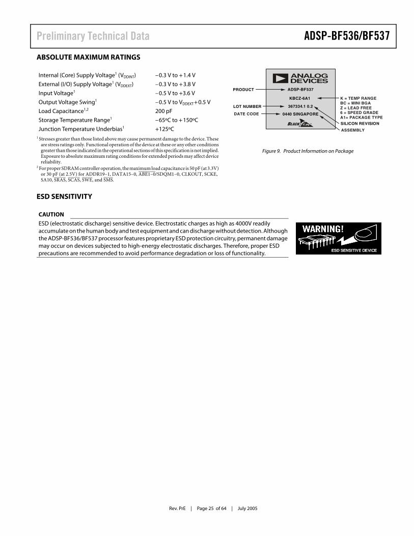
ADSP-BF536/BF537Preliminary Technical Data
Rev. PrE | Page 25 of 64 | July 2005
ABSOLUTE MAXIMUM RATINGS
ESD SENSITIVITY
Internal (Core) Supply Voltage1 (VDDINT)
1 Stresses greater than those listed above may cause permanent damage to the device. These are stress ratings only. Functional operation of the device at these or any other conditions greater than those indicated in the operational sections of this specification is not implied. Exposure to absolute maximum rating conditions for extended periods may affect device reliability.
–0.3 V to +1.4 V
External (I/O) Supply Voltage1 (VDDEXT) –0.3 V to +3.8 V
Input Voltage1 –0.5 V to +3.6 V
Output Voltage Swing1 –0.5 V to VDDEXT +0.5 V
Load Capacitance1,2
2 For proper SDRAM controller operation, the maximum load capacitance is 50 pF (at 3.3V) or 30 pF (at 2.5V) for ADDR19–1, DATA15–0, ABE1–0/SDQM1–0, CLKOUT, SCKE, SA10, SRAS, SCAS, SWE, and SMS.
200 pF
Storage Temperature Range1 –65ºC to +150ºC
Junction Temperature Underbias1 +125ºC
Figure 9. Product Information on Package
367334.1 0.2
SILICON REVISION
LOT NUMBER
KBCZ-6A1
PRODUCT
DATE CODE
ASSEMBLY
K = TEMP RANGEBC = MINI BGAZ = LEAD FREE6 = SPEED GRADEA1= PACKAGE TYPE
B
ADSP-BF537
a
0440 SINGAPORE
CAUTION
ESD (electrostatic discharge) sensitive device. Electrostatic charges as high as 4000V readily accumulate on the human body and test equipment and can discharge without detection. Although the ADSP-BF536/BF537 processor features proprietary ESD protection circuitry, permanent damage may occur on devices subjected to high-energy electrostatic discharges. Therefore, proper ESD precautions are recommended to avoid performance degradation or loss of functionality.

Rev. PrE | Page 26 of 64 | July 2005
ADSP-BF536/BF537 Preliminary Technical Data
TIMING SPECIFICATIONS
Table 10 through Table 13 describe the timing requirements for the ADSP-BF536/BF537 processor clocks. Take care in selecting MSEL, SSEL, and CSEL ratios so as not to exceed the maximum core clock and system clock. Table 14 describes Phase-Locked Loop operating conditions.
Table 10. Core Clock Requirements—600 MHz Speed Grade1
Parameter Minimum Maximum Unit
fCCLK Core Clock Frequency (VDDINT =1.2 V minimum) 600 MHz
fCCLK Core Clock Frequency (VDDINT =1.045 V minimum) TBD MHz
fCCLK Core Clock Frequency (VDDINT =0.95 V minimum) TBD MHz
fCCLK Core Clock Frequency (VDDINT =0.85 V minimum) TBD MHz
fCCLK Core Clock Frequency (VDDINT =0.8 V ) TBD MHz1 The speed grade of a given part is printed on the chip’s package as shown in Figure 9 on Page 25 and can also be seen on the “Ordering Guide” on page 64. It stands for the
Maximum allowed CCLK frequency at VDDINT = 1.2V and the maximum allowed VCO frequency at any supply voltage.
Table 11. Core Clock Requirements—500 MHz Speed Grade1
Parameter Minimum Maximum Unit
fCCLK Core Clock Frequency (VDDINT =1.2 V minimum) 500 MHz
fCCLK Core Clock Frequency (VDDINT =1.045 V minimum) TBD MHz
fCCLK Core Clock Frequency (VDDINT =0.95 V minimum) TBD MHz
fCCLK Core Clock Frequency (VDDINT =0.85 V minimum) TBD MHz
fCCLK Core Clock Frequency (VDDINT =0.8 V ) TBD MHz1 The speed grade of a given part is printed on the chip’s package as shown in Figure 9 on Page 25 and can also be seen on the “Ordering Guide” on page 64. It stands for the
Maximum allowed CCLK frequency at VDDINT = 1.2V and the maximum allowed VCO frequency at any supply voltage.
Table 12. Core Clock Requirements—400 MHz Speed Grade1
Parameter Minimum Maximum Unit
fCCLK Core Clock Frequency (VDDINT =1.14 V minimum) 400 MHz
fCCLK Core Clock Frequency (VDDINT =1.045 V minimum) TBD MHz
fCCLK Core Clock Frequency (VDDINT =0.95 V minimum) TBD MHz
fCCLK Core Clock Frequency (VDDINT =0.85 V minimum) TBD MHz
fCCLK Core Clock Frequency (VDDINT =0.8 V ) TBD MHz1 The speed grade of a given part is printed on the chip’s package as shown in Figure 9 on Page 25 and can also be seen on the “Ordering Guide” on page 64. It stands for the
Maximum allowed CCLK frequency at VDDINT = 1.2V and the maximum allowed VCO frequency at any supply voltage.
Table 13. Core Clock Requirements—300 MHz Speed Grade1
Parameter Minimum Maximum Unit
fCCLK Core Clock Frequency (VDDINT =1.14 V minimum) 300 MHz
fCCLK Core Clock Frequency (VDDINT =1.045 V minimum) TBD MHz
fCCLK Core Clock Frequency (VDDINT =0.95 V minimum) TBD MHz
fCCLK Core Clock Frequency (VDDINT =0.85 V minimum) TBD MHz
fCCLK Core Clock Frequency (VDDINT =0.8 V ) TBD MHz1 The speed grade of a given part is printed on the chip’s package as shown in Figure 9 on Page 25 and can also be seen on the “Ordering Guide” on page 64. It stands for the
Maximum allowed CCLK frequency at VDDINT = 1.2V and the maximum allowed VCO frequency at any supply voltage.

ADSP-BF536/BF537Preliminary Technical Data
Rev. PrE | Page 27 of 64 | July 2005
Table 14. Phase-Locked Loop Operating Conditions
Parameter Minimum Maximum Unit
fVCO Voltage Controlled Oscillator (VCO) Frequency 50 Speed Grade1 MHz1 The speed grade of a given part is printed on the chip’s package as shown in Figure 9 on Page 25 and can also be seen on the “Ordering Guide” on page 64. It stands for the
Maximum allowed CCLK frequency at VDDINT = 1.2V and the maximum allowed VCO frequency at any supply voltage.
Table 15. System Clock Requirements
Parameter Condition Minimum Maximum Unit
182 MBGA
fSCLK VDDEXT = 3.3 V, VDDINT >= TBD V TBD MHz
fSCLK VDDEXT = 3.3 V, VDDINT < TBD V TBD MHz
fSCLK VDDEXT = 2.5 V, VDDINT >= TBD V TBD MHz
fSCLK VDDEXT = 2.5 V, VDDINT < TBD V TBD MHz
208 MBGA
fSCLK VDDEXT = 3.3 V, VDDINT >= TBD V TBD MHz
fSCLK VDDEXT = 3.3 V, VDDINT < TBD V TBD MHz
fSCLK VDDEXT = 2.5 V, VDDINT >= TBD V TBD MHz
fSCLK VDDEXT = 2.5 V, VDDINT < TBD V TBD MHz
Table 16. Clock Input and Reset Timing
Parameter Minimum Maximum Unit
Timing Requirements
tCKIN CLKIN Period1 25.0 100.0 ns
tCKINL CLKIN Low Pulse2 10.0 ns
tCKINH CLKIN High Pulse2 10.0 ns
tBUFDLAY CLKIN to CLKBUF delay TBD ns
tWRST RESET Asserted Pulsewidth Low3 11 tCKIN ns1 Combinations of the CLKIN frequency and the PLL clock multiplier must not exceed the allowed fVCO, fCCLK, and fSCLK settings discussed in Table 10 through Table 15. Since
by default the PLL is multiplying the CLKIN frequency by 10, 300 MHz and 400MHz speed grade parts can not use the full CLKIN period range.2 Applies to bypass mode and non-bypass mode.3 Applies after power-up sequence is complete. At power-up, the processor’s internal phase-locked loop requires no more than 2000 CLKIN cycles, while RESET is asserted,
assuming stable power supplies and CLKIN (not including start-up time of external clock oscillator).
Figure 10. Clock and Reset Timing
RESET
CLKIN
tCKINH
tCKIN
tCKINL
tWRST
CLKBUF
tBUFDLAYtBUFDLAY

Rev. PrE | Page 28 of 64 | July 2005
ADSP-BF536/BF537 Preliminary Technical Data
Asynchronous Memory Read Cycle Timing
Table 17. Asynchronous Memory Read Cycle Timing
Parameter Minimum Maximum Unit
Timing Requirements
tSDAT DATA15–0 Setup Before CLKOUT 2.1 ns
tHDAT DATA15–0 Hold After CLKOUT 0.8 ns
tSARDY ARDY Setup Before CLKOUT 4.0 ns
tHARDY ARDY Hold After CLKOUT 0.0 ns
Switching Characteristic
tDO Output Delay After CLKOUT1
1 Output pins include AMS3–0, ABE1–0, ADDR19–1, AOE, ARE.
6.0 ns
tHO Output Hold After CLKOUT 1 0.8 ns
Figure 11. Asynchronous Memory Read Cycle Timing
tDO
tSDAT
CLKOUT
AMSx
ABE1–0
tHO
BE, ADDRESS
READ
tHDAT
DATA15–0
AOE
tDO
tSARDY
tHARDY
ACCESS EXTENDED3 CYCLES
HOLD1 CYCLE
ARE
tHARDY
ARDY
ADDR19–1
SETUP2 CYCLES
PROGRAMMED READ ACCESS4 CYCLES
tHO
tSARDY

ADSP-BF536/BF537Preliminary Technical Data
Rev. PrE | Page 29 of 64 | July 2005
Asynchronous Memory Write Cycle Timing
Table 18. Asynchronous Memory Write Cycle Timing
Parameter Minimum Maximum Unit
Timing Requirements
tSARDY ARDY Setup Before CLKOUT 4.0 ns
tHARDY ARDY Hold After CLKOUT 0.0 ns
Switching Characteristic
tDDAT DATA15–0 Disable After CLKOUT 6.0 ns
tENDAT DATA15–0 Enable After CLKOUT 1.0 ns
tDO Output Delay After CLKOUT1
1 Output pins include AMS3–0, ABE1–0, ADDR19–1, DATA15–0, AOE, AWE.
6.0 ns
tHO Output Hold After CLKOUT 1 0.8 ns
Figure 12. Asynchronous Memory Write Cycle Timing
tDO
tENDAT
CLKOUT
AMSx
ABE1–0BE, ADDRESS
tHO
WRITE DATA
tDDAT
DATA15–0
AWE
tSARDY tHARDY
SETUP2 CYCLES
PROGRAMMED WRITEACCESS 2 CYCLES
ACCESSEXTENDED
1 CYCLEHOLD
1 CYCLE
ARDY
ADDR19–1
tHO
tSARDY
tDO
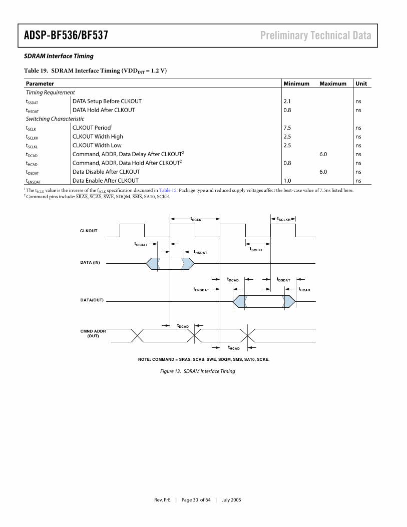
Rev. PrE | Page 30 of 64 | July 2005
ADSP-BF536/BF537 Preliminary Technical Data
SDRAM Interface Timing
Table 19. SDRAM Interface Timing (VDDINT = 1.2 V)
Parameter Minimum Maximum Unit
Timing Requirement
tSSDAT DATA Setup Before CLKOUT 2.1 ns
tHSDAT DATA Hold After CLKOUT 0.8 ns
Switching Characteristic
tSCLK CLKOUT Period1
1 The tSCLK value is the inverse of the fSCLK specification discussed in Table 15. Package type and reduced supply voltages affect the best-case value of 7.5ns listed here.
7.5 ns
tSCLKH CLKOUT Width High 2.5 ns
tSCLKL CLKOUT Width Low 2.5 ns
tDCAD Command, ADDR, Data Delay After CLKOUT2
2 Command pins include: SRAS, SCAS, SWE, SDQM, SMS, SA10, SCKE.
6.0 ns
tHCAD Command, ADDR, Data Hold After CLKOUT2 0.8 ns
tDSDAT Data Disable After CLKOUT 6.0 ns
tENSDAT Data Enable After CLKOUT 1.0 ns
Figure 13. SDRAM Interface Timing
tHCAD
tHCAD
tDSDAT
tDCAD
tSSDAT
tDCAD
tENSDAT
tHSDATtSCLKL
tSCLKHtSCLK
CLKOUT
DATA (IN)
DATA(OUT)
CMND ADDR(OUT)
NOTE: COMMAND = SRAS, SCAS, SWE, SDQM, SMS, SA10, SCKE.
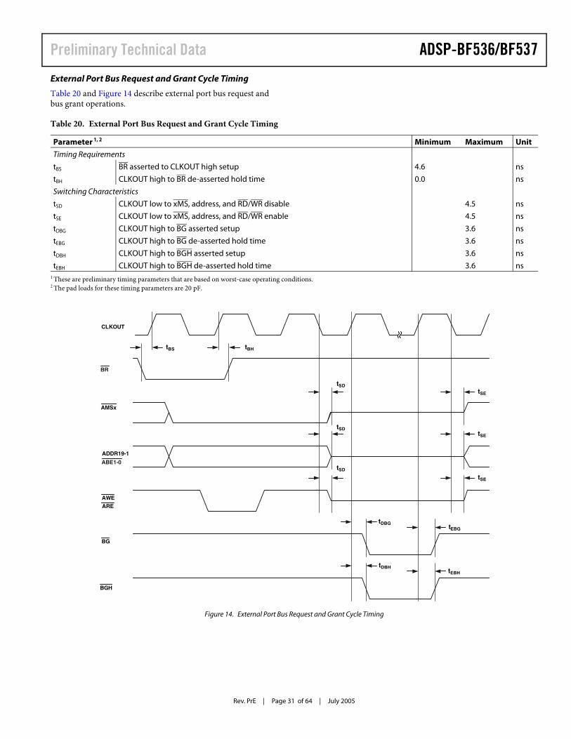
ADSP-BF536/BF537Preliminary Technical Data
Rev. PrE | Page 31 of 64 | July 2005
External Port Bus Request and Grant Cycle Timing
Table 20 and Figure 14 describe external port bus request and bus grant operations.
Table 20. External Port Bus Request and Grant Cycle Timing
Parameter 1, 2 Minimum Maximum Unit
Timing Requirements
tBS BR asserted to CLKOUT high setup 4.6 ns
tBH CLKOUT high to BR de-asserted hold time 0.0 ns
Switching Characteristics
tSD CLKOUT low to xMS, address, and RD/WR disable 4.5 ns
tSE CLKOUT low to xMS, address, and RD/WR enable 4.5 ns
tDBG CLKOUT high to BG asserted setup 3.6 ns
tEBG CLKOUT high to BG de-asserted hold time 3.6 ns
tDBH CLKOUT high to BGH asserted setup 3.6 ns
tEBH CLKOUT high to BGH de-asserted hold time 3.6 ns1 These are preliminary timing parameters that are based on worst-case operating conditions.2 The pad loads for these timing parameters are 20 pF.
Figure 14. External Port Bus Request and Grant Cycle Timing
tBH
ADDR19-1
AMSx
CLKOUT
tBS
tSD
tSD
tSD
tDBG
tDBH
tSE
tSE
tSE
tEBG
tEBH
BG
AWE
BGH
ARE
BR
ABE1-0
Rev. PrE | Page 32 of 64 | July 2005
ADSP-BF536/BF537 Preliminary Technical Data
External DMA Request Timing
Table 21 and Figure 15 describe the External DMA Request operations.
Table 21. External DMA Request Timing
Parameter Minimum Maximum Unit
Timing Parameters
tDR DMARx asserted to CLKOUT high setup TBD TBD ns
tDH CLKOUT high to DMARx de-asserted hold time TBD TBD ns
Switching Characteristics
tDO Output delay after CLKOUT1 TBD TBD ns
tHO Output hold after CLKOUT1 TBD TBD ns1 System Outputs=DATA15–0, ADDR19–1, ABE1–0, AOE, ARE, AWE, AMS3–0, SRAS, SCAS, SWE, SCKE, CLKOUT, SA10, SMS, SCL, SDA, TSCLK0, TFS0, RFS0, RSCLK0,
DT0PRI, DT0SEC, PF15–0, PG15–0, PH15–0, MDC, MDIO, RTX0, TD0, EMU, XTAL, CLKBUF, VROUT.
Figure 15. External DMA Request Timing
AMSx
CLKOUT
tDR
tHO
DMAR0/1
tDO
tDH

ADSP-BF536/BF537Preliminary Technical Data
Rev. PrE | Page 33 of 64 | July 2005
Parallel Peripheral Interface Timing
Table 22 and Figure 16 on Page 33, Figure 17 on Page 36, and Figure 18 on Page 37 describe Parallel Peripheral Interface operations.
Table 22. Parallel Peripheral Interface Timing
Parameter Minimum Maximum Unit
Timing Requirements
tPCLKW PPI_CLK Width1 6.0 ns
tPCLK PPI_CLK Period1 15.0 ns
Timing Requirements - GP Input and Frame Capture Modes
tSFSPE External Frame Sync Setup Before PPI_CLK 3.0 ns
tHFSPE External Frame Sync Hold After PPI_CLK 3.0 ns
tSDRPE Receive Data Setup Before PPI_CLK 2.0 ns
tHDRPE Receive Data Hold After PPI_CLK 4.0 ns
Switching Characteristics - GP Output and Frame Capture Modes
tDFSPE Internal Frame Sync Delay After PPI_CLK 10.0 ns
tHOFSPE Internal Frame Sync Hold After PPI_CLK 0.0 ns
tDDTPE Transmit Data Delay After PPI_CLK 10.0 ns
tHDTPE Transmit Data Hold After PPI_CLK 0.0 ns1 PPI_CLK frequency cannot exceed fSCLK/2
Figure 16. Parallel Peripheral Interface Timing
tDDTPE
tHDTPE
PPI_CLK
PPI_FS1
PPIx
DRIVEEDGE
SAMPLEEDGE
tSFSPE tHFSPE
tPCLKW
tDFSPE
tHOFSPE
PPI_FS2
tSDRPE tHDRPE

Rev. PrE | Page 34 of 64 | July 2005
ADSP-BF536/BF537 Preliminary Technical Data
Serial Ports
Table 23 through Table 28 on Page 35 and Figure 17 on Page 36 through Figure 19 on Page 38 describe Serial Port operations.
Table 23. Serial Ports—External Clock
Parameter Minimum Maximum Unit
Timing Requirements
tSFSE TFS/RFS Setup Before TSCLK/RSCLK1 3.0 ns
tHFSE TFS/RFS Hold After TSCLK/RSCLK1 3.0 ns
tSDRE Receive Data Setup Before RSCLK1 3.0 ns
tHDRE Receive Data Hold After RSCLK1 3.0 ns
tSCLKEW TSCLK/RSCLK Width 4.5 ns
tSCLKE TSCLK/RSCLK Period 15.0 ns1 Referenced to sample edge.
Table 24. Serial Ports—Internal Clock
Parameter Minimum Maximum Unit
Timing Requirements
tSFSI TFS/RFS Setup Before TSCLK/RSCLK1 8.0 ns
tHFSI TFS/RFS Hold After TSCLK/RSCLK1 –2.0 ns
tSDRI Receive Data Setup Before RSCLK1 6.0 ns
tHDRI Receive Data Hold After RSCLK1 0.0 ns
tSCLKEW TSCLK/RSCLK Width 4.5 ns
tSCLKE TSCLK/RSCLK Period 15.0 ns1 Referenced to sample edge.
Table 25. Serial Ports—External Clock
Parameter Minimum Maximum Unit
Switching Characteristics
tDFSE TFS/RFS Delay After TSCLK/RSCLK (Internally Generated TFS/RFS)1 10.0 ns
tHOFSE TFS/RFS Hold After TSCLK/RSCLK (Internally Generated TFS/RFS)1 0.0 ns
tDDTE Transmit Data Delay After TSCLK1 10.0 ns
tHDTE Transmit Data Hold After TSCLK1 0.0 ns1 Referenced to drive edge.
Table 26. Serial Ports—Internal Clock
Parameter Minimum Maximum Unit
Switching Characteristics
tDFSI TFS/RFS Delay After TSCLK/RSCLK (Internally Generated TFS/RFS)1 3.0 ns
tHOFSI TFS/RFS Hold After TSCLK/RSCLK (Internally Generated TFS/RFS)1 −1.0 ns
tDDTI Transmit Data Delay After TSCLK1 3.0 ns
tHDTI Transmit Data Hold After TSCLK1 −2.0 ns
tSCLKIW TSCLK/RSCLK Width 4.5 ns1 Referenced to drive edge.
ADSP-BF536/BF537Preliminary Technical Data
Rev. PrE | Page 35 of 64 | July 2005
Table 27. Serial Ports—Enable and Three-State
Parameter Minimum Maximum Unit
Switching Characteristics
tDTENE Data Enable Delay from External TSCLK1 0.0 ns
tDDTTE Data Disable Delay from External TSCLK1 10.0 ns
tDTENI Data Enable Delay from Internal TSCLK1 –2.0 ns
tDDTTI Data Disable Delay from Internal TSCLK1 3.0 ns1 Referenced to drive edge.
Table 28. External Late Frame Sync
Parameter Minimum Maximum Unit
Switching Characteristics
tDDTLFSE Data Delay from Late External TFS or External RFS with MCE = 1, MFD = 01,2 10.0 ns
tDTENLFSE Data Enable from late FS or MCE = 1, MFD = 01,2 0.0 ns1 MCE = 1, TFS enable and TFS valid follow tDDTENFS and tDDTLFSE.2 If external RFS/TFS setup to RSCLK/TSCLK > tSCLKE/2 then tDDTLSCK and tDTENLSCK apply, otherwise tDDTLFSE and tDTENLFS apply.
Rev. PrE | Page 36 of 64 | July 2005
ADSP-BF536/BF537 Preliminary Technical Data
Figure 17. Serial Ports
DT
DT
tDDTTEtDDTENE
tDDTTItDDTENI
DRIVEEDGE
DRIVEEDGE
DRIVEEDGE
DRIVEEDGE
TSCLK / RSCLK
TSCLK / RSCLKTSCLK (EXT)TFS ("LATE", EXT.)
TSCLK (INT)TFS ("LATE", INT.)
tSDRI
RSCLK
RFS
DR
DRIVEEDGE
SAMPLEEDGE
tHDRI
tSFSI tHFSI
tDFSE
tHOFSE
tSCLKIW
DATA RECEIVE- INTERNAL CLOCK
tSDRE
DATA RECEIVE- EXTERNAL CLOCK
RSCLK
RFS
DR
DRIVEEDGE
SAMPLEEDGE
tHDRE
tSFSE tHFSE
tDFSE
tSCLKEW
tHOFSE
NOTE: EITHER THE RISING EDGE OR FALLING EDGE OF RCLK, TCLK CAN BE USED AS THE ACTIVE SAMPLING EDGE.
tDDTI
tHDTI
TSCLK
TFS
DT
DRIVEEDGE
SAMPLEEDGE
tSFSI tHFSI
tSCLKIW
tDFSI
tHOFSI
DATA TRANSMIT- INTERNAL CLOCK
tDDTE
tHDTE
TSCLK
TFS
DT
DRIVEEDGE
SAMPLEEDGE
tSFSE tHFSE
tDFSE
tSCLKEW
tHOFSE
DATA TRANSMIT- EXTERNAL CLOCK
NOTE: EITHER THE RISING EDGE OR FALLING EDGE OF RCLK OR TCLK CAN BE USED AS THE ACTIVE SAMPLING EDGE.

ADSP-BF536/BF537Preliminary Technical Data
Rev. PrE | Page 37 of 64 | July 2005
Figure 18. External Late Frame Sync (Frame Sync Setup < tSCLKE/2)
tDDTLFSE
tSFSE/I
tHDTE/I
RSCLK
DRIVE DRIVESAMPLE
RFS
DT 2ND BIT1ST BIT
tDTENLFSE
tDDTE/I
tHOFSE/I
tDTENLFSE
tSFSE/I
tHDTE/I
DRIVE DRIVESAMPLE
DT
TSCLK
TFS
2ND BIT1ST BIT
tDDTLFSE
tDDTE/I
tHOFSE/I
EXTERNAL RFS WITH MCE = 1, MFD = 0
LATE EXTERNAL TFS

Rev. PrE | Page 38 of 64 | July 2005
ADSP-BF536/BF537 Preliminary Technical Data
Figure 19. External Late Frame Sync (Frame Sync Setup > tSCLKE/2)
DT
RSCLK
RFS
tSFSE/I tHOFSE/I
tDTENLSCK
tDDTE/I
tHDTE/I
tDDTLSCK
DRIVE SAMPLE
1ST BIT 2ND BIT
DRIVE
DT
TSCLK
TFS
tSFSE/I tHOFSE/I
tDTENLSCK
tDDTE/I
tHDTE/I
tDDTLSCK
DRIVE SAMPLE
1ST BIT 2ND BIT
DRIVE
LATE EXTERNAL TFS
EXTERNAL RFS WITH MCE=1, MFD=0

ADSP-BF536/BF537Preliminary Technical Data
Rev. PrE | Page 39 of 64 | July 2005
Serial Peripheral Interface (SPI) Port—Master Timing
Table 29 and Figure 20 describe SPI port master operations.
Table 29. Serial Peripheral Interface (SPI) Port—Master Timing
Parameter Minimum Maximum Unit
Timing Requirements
tSSPIDM Data input valid to SCK edge (data input setup) 7.5 ns
tHSPIDM SCK sampling edge to data input invalid –1.5 ns
Switching Characteristics
tSDSCIM SPISELx low to first SCK edge (x=0 or 1) 2tSCLK –1.5 ns
tSPICHM Serial clock high period 2tSCLK –1.5 ns
tSPICLM Serial clock low period 2tSCLK –1.5 ns
tSPICLK Serial clock period 4tSCLK –1.5 ns
tHDSM Last SCK edge to SPISELx high (x=0 or 1) 2tSCLK –1.5 ns
tSPITDM Sequential transfer delay 2tSCLK –1.5 ns
tDDSPIDM SCK edge to data out valid (data out delay) 0 6 ns
tHDSPIDM SCK edge to data out invalid (data out hold) –1.0 4.0 ns
Figure 20. Serial Peripheral Interface (SPI) Port—Master Timing
tSSPIDM tHSPIDM
tHDSPIDM
LSBMSB
tHSPIDM
tDDSPIDM
MOSI(OUTPUT)
MISO(INPUT)
SPISELx(OUTPUT)
SCK(CPOL = 0)(OUTPUT)
SCK(CPOL = 1)(OUTPUT)
tSPICHM tSPICLM
tSPICLM
tSPICLK
tSPICHM
tHDSM tSPITDM
tHDSPIDM
LSB VALID
LSBMSB
MSB VALID
tHSPIDM
tDDSPIDM
MOSI(OUTPUT)
MISO(INPUT)
tSSPIDM
CPHA=1
CPHA=0
MSB VALID
tSDSCIM
tSSPIDM
LSB VALID
Rev. PrE | Page 40 of 64 | July 2005
ADSP-BF536/BF537 Preliminary Technical Data
Serial Peripheral Interface (SPI) Port—Slave Timing
Table 30 and Figure 21 describe SPI port slave operations.
Table 30. Serial Peripheral Interface (SPI) Port—Slave Timing
Parameter Minimum Maximum Unit
Timing Requirements
tSPICHS Serial clock high period 2tSCLK –1.5 ns
tSPICLS Serial clock low period 2tSCLK –1.5 ns
tSPICLK Serial clock period 4tSCLK –1.5 ns
tHDS Last SCK edge to SPISS not asserted 2tSCLK –1.5 ns
tSPITDS Sequential Transfer Delay 2tSCLK –1.5 ns
tSDSCI SPISS assertion to first SCK edge 2tSCLK –1.5 ns
tSSPID Data input valid to SCK edge (data input setup) 1.6 ns
tHSPID SCK sampling edge to data input invalid 1.6 ns
Switching Characteristics
tDSOE SPISS assertion to data out active 0 8 ns
tDSDHI SPISS deassertion to data high impedance 0 8 ns
tDDSPID SCK edge to data out valid (data out delay) 0 10 ns
tHDSPID SCK edge to data out invalid (data out hold) 0 10 ns
Figure 21. Serial Peripheral Interface (SPI) Port—Slave Timing
tHSPID
tDDSPID tDSDHI
LSBMSB
MSB VALID
tHSPID
tDSOE tDDSPIDtHDSPID
MISO(OUTPUT)
MOSI(INPUT)
tSSPID
SPISS(INPUT)
SCK(CPOL = 0)
(INPUT)
SCK(CPOL = 1)
(INPUT)
tSDSCI
tSPICHS tSPICLS
tSPICLS
tSPICLK tHDS
tSPICHS
tSSPID
tHSPID
tDSDHI
LSB VALID
MSB
MSB VALID
tDSOE tDDSPID
MISO(OUTPUT)
MOSI(INPUT)
tSSPID
LSB VALID
LSB
CPHA=1
CPHA=0
tSPITDS
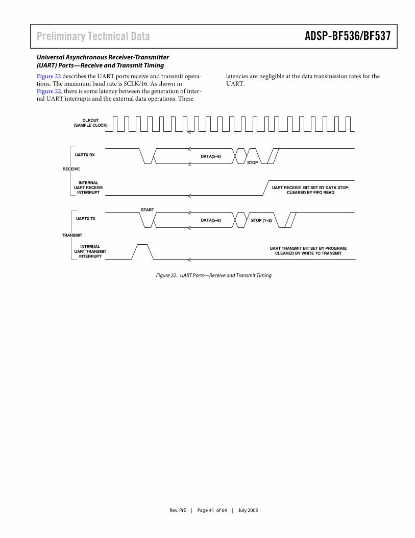
ADSP-BF536/BF537Preliminary Technical Data
Rev. PrE | Page 41 of 64 | July 2005
Universal Asynchronous Receiver-Transmitter (UART) Ports—Receive and Transmit Timing
Figure 22 describes the UART ports receive and transmit opera-tions. The maximum baud rate is SCLK/16. As shown in Figure 22, there is some latency between the generation of inter-nal UART interrupts and the external data operations. These
latencies are negligible at the data transmission rates for the UART.
Figure 22. UART Ports—Receive and Transmit Timing
UARTX RX DATA(5–8)
INTERNALUART RECEIVE
INTERRUPTUART RECEIVE BIT SET BY DATA STOP;
CLEARED BY FIFO READ
CLKOUT(SAMPLE CLOCK)
UARTX TX DATA(5–8) STOP (1–2)
INTERNALUART TRANSMIT
INTERRUPT
UART TRANSMIT BIT SET BY PROGRAM;CLEARED BY WRITE TO TRANSMIT
START
STOP
TRANSMIT
RECEIVE

Rev. PrE | Page 42 of 64 | July 2005
ADSP-BF536/BF537 Preliminary Technical Data
General-Purpose Port Timing
Table 31 and Figure 23 describe general-purpose port operations.
Table 31. General-Purpose Port Timing
Parameter Minimum Maximum Unit
Timing Requirement
tWFI General-purpose port pin input pulsewidth tSCLK + 1 ns
tGPPIS General-purpose port pin input setup TBD ns
tGPPIH General-purpose port pin input hold TBD ns
Switching Characteristic
tGPOD General-purpose port pin output delay from CLKOUT low 0 6 ns
Figure 23. General-Purpose Port Timing
GPP INPUT
GPP OUTPUT
CLKOUT
tGPOD
tGPPIS tGPPIH
tWFI

ADSP-BF536/BF537Preliminary Technical Data
Rev. PrE | Page 43 of 64 | July 2005
Timer Cycle Timing
Table 32 and Figure 24 describe timer expired operations. The input signal is asynchronous in “width capture mode” and “external clock mode” and has an absolute maximum input fre-quency of fSCLK/2 MHz.
Table 32. Timer Cycle Timing
Parameter Minimum Maximum Unit
Timing Characteristics
tWL Timer pulsewidth input low1 (measured in SCLK cycles) 1 SCLK
tWH Timer pulsewidth input high1 (measured in SCLK cycles) 1 SCLK
tTIS Timer input setup time before CLKOUT low TBD ns
tTIH Timer input hold time after CLKOUT low TBD ns
Switching Characteristic
tHTO Timer pulsewidth output2 (measured in SCLK cycles) 1 (232–1) SCLK
tTOD Timer output update delay after CLKOUT low 0 TBD ns1 The minimum pulsewidths apply for TMRx signals in width capture and external clock modes. They also apply to the PF15 or PPI_CLK signals in PWM output mode.2 The minimum time for tHTO is one cycle, and the maximum time for tHTO equals (232–1) cycles.
Figure 24. Timer Cycle Timing
TIMER INPUT
TIMER OUTPUT
CLKOUT
tTOD
tTIS tTIH
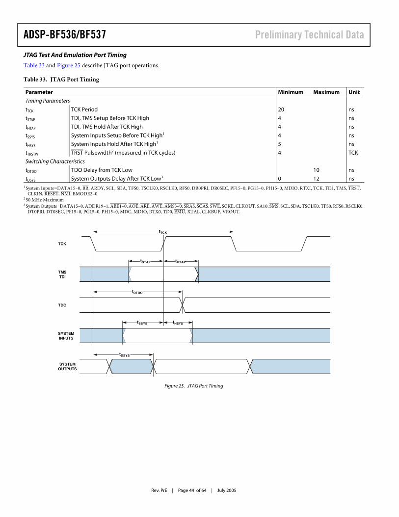
Rev. PrE | Page 44 of 64 | July 2005
ADSP-BF536/BF537 Preliminary Technical Data
JTAG Test And Emulation Port Timing
Table 33 and Figure 25 describe JTAG port operations.
Table 33. JTAG Port Timing
Parameter Minimum Maximum Unit
Timing Parameters
tTCK TCK Period 20 ns
tSTAP TDI, TMS Setup Before TCK High 4 ns
tHTAP TDI, TMS Hold After TCK High 4 ns
tSSYS System Inputs Setup Before TCK High1 4 ns
tHSYS System Inputs Hold After TCK High1 5 ns
tTRSTW TRST Pulsewidth2 (measured in TCK cycles) 4 TCK
Switching Characteristics
tDTDO TDO Delay from TCK Low 10 ns
tDSYS System Outputs Delay After TCK Low3 0 12 ns1 System Inputs=DATA15–0, BR, ARDY, SCL, SDA, TFS0, TSCLK0, RSCLK0, RFS0, DR0PRI, DR0SEC, PF15–0, PG15–0, PH15–0, MDIO, RTXI, TCK, TD1, TMS, TRST,
CLKIN, RESET, NMI, BMODE2–0.2 50 MHz Maximum3 System Outputs=DATA15–0, ADDR19–1, ABE1–0, AOE, ARE, AWE, AMS3–0, SRAS, SCAS, SWE, SCKE, CLKOUT, SA10, SMS, SCL, SDA, TSCLK0, TFS0, RFS0, RSCLK0,
DT0PRI, DT0SEC, PF15–0, PG15–0, PH15–0, MDC, MDIO, RTX0, TD0, EMU, XTAL, CLKBUF, VROUT.
Figure 25. JTAG Port Timing
TMSTDI
TDO
SYSTEMINPUTS
SYSTEMOUTPUTS
TCK
tTCK
tHTAPtSTAP
tDTDO
tSSYS tHSYS
tDSYS
ADSP-BF536/BF537Preliminary Technical Data
Rev. PrE | Page 45 of 64 | July 2005
TWI Controller Timing
Table 34 through Table 41 and Figure 26 through Figure 29 describe the TWI Controller operations.
Table 34. TWI Controller Timing: Bus Start/Stop Bits, Slave Mode, 100 kHz
Parameter Minimum Maximum Unit
tSU:STA Start condition setup time TBD - ns
tHD:STA Start condition hold time TBD - ns
tSU:STO Stop condition setup time TBD - ns
tHD:STO Stop condition hold time TBD - ns
Table 35. TWI Controller Timing: Bus Start/Stop Bits, Slave Mode, 400 kHz
Parameter Minimum Maximum Unit
tSU:STA Start condition setup time TBD - ns
tHD:STA Start condition hold time TBD - ns
tSU:STO Stop condition setup time TBD - ns
tHD:STO Stop condition hold time TBD - ns
Table 36. TWI Controller Timing: Bus Data Requirements, Slave Mode, 100 kHz
Parameter Minimum Maximum Unit
tHIGH Clock high time TBD - µs
tLOW Clock low time TBD - µs
tR SDA and SCL rise time - TBD ns
tF SDA and SCL fall time - TBD ns
tSU:STA Start condition setup time TBD - µs
tHD:STA Start condition hold time TBD - µs
tHD:DAT Data input hold time TBD - ns
tSU:DAT Data input setup time1 TBD - ns
tSU:STO Stop condition setup time TBD - µs
tTAA Output valid from clock2 - TBD ns
tBUF Bus free time TBD - µs
CB Bus capacitive loading - TBD pF1 As a transmitter, the device must provide this internal minimum delay time to bridge the undefined region (min. TBD ns) of the falling edge of SCL to avoid unintended
generation of START or STOP conditions.2 A Fast mode TWI bus device can be used in a Standard mode TWI bus system, but the requirement TSU:DAT >= 250 ns must then be met. This will automatically be the case if
the device does not stretch the LOW period of the SCL signal. If such a device does stretch the LOW period of the SCL signal, it must output the next data bit to the SDA line. Before the SCL line is released, TR max. + TSU:DAT = 1000 + 250 = 1250 ns (according to the Standard mode I2C bus specification).
Rev. PrE | Page 46 of 64 | July 2005
ADSP-BF536/BF537 Preliminary Technical Data
Table 37. TWI Controller Timing: Bus Data Requirements, Slave Mode, 400 kHz
Parameter Minimum Maximum Unit
tHIGH Clock high time TBD - µs
tLOW Clock low time TBD - µs
tR SDA and SCL rise time TBD TBD ns
tF SDA and SCL fall time TBD TBD ns
tSU:STA Start condition setup time TBD - µs
tHD:STA Start condition hold time TBD - µs
tHD:DAT Data input hold time TBD TBD µs
tSU:DAT Data input setup time1 TBD - ns
tSU:STO Stop condition setup time TBD - µs
tTAA Output valid from clock - - ns
tBUF Bus free time TBD - µs
CB Bus capacitive loading - TBD pF1 As a transmitter, the device must provide this internal minimum delay time to bridge the undefined region (min. TBD ns) of the falling edge of SCL to avoid unintended
generation of START or STOP conditions.
Table 38. TWI Controller Timing: Bus Start/Stop Bits, Master Mode, 100 kHz
Parameter Minimum Maximum Unit
tSU:STA Start condition setup time TBD - ns
tHD:STA Start condition hold time TBD - ns
tSU:STO Stop condition setup time TBD - ns
tHD:STO Stop condition hold time TBD - ns
Table 39. TWI Controller Timing: Bus Start/Stop Bits, Master Mode, 400 kHz
Parameter Minimum Maximum Unit
tSU:STA Start condition setup time TBD - ns
tHD:STA Start condition hold time TBD - ns
tSU:STO Stop condition setup time TBD - ns
tHD:STO Stop condition hold time TBD - ns
Table 40. TWI Controller Timing: Bus Data Requirements, Master Mode, 100 kHz
Parameter Minimum Maximum Unit
tHIGH Clock high time TBD - ms
tLOW Clock low time TBD - ms
tR SDA and SCL rise time - TBD ns
tF SDA and SCL fall time - TBD ns
tSU:STA Start condition setup time TBD - ms
tHD:STA Start condition hold time TBD - ms
tHD:DAT Data input hold time TBD - ns
tSU:DAT Data input setup time1 TBD - ns
tSU:STO Stop condition setup time TBD - ms
tTAA Output valid from clock - TBD ns
tBUF Bus free time TBD - ms
CB Bus capacitive loading - TBD pF1 A Fast mode TWI bus device can be used in a Standard mode TWI bus system, but the requirement TSU:DAT >= 250 ns must then be met. This will automatically be the case if
the device does not stretch the LOW period of the SCL signal. If such a device does stretch the LOW period of the SCL signal, it must output the next data bit to the SDA line. Before the SCL line is released, TR max. + TSU:DAT = 1000 + 250 = 1250 ns (according to the Standard mode I2C bus specification).

ADSP-BF536/BF537Preliminary Technical Data
Rev. PrE | Page 47 of 64 | July 2005
Table 41. TWI Controller Timing: Bus Data Requirements, Master Mode, 400 kHz
Parameter Minimum Maximum Unit
tHIGH Clock high time TBD - ms
tLOW Clock low time TBD - ms
tR SDA and SCL rise time TBD TBD ns
tF SDA and SCL fall time TBD TBD ns
tSU:STA Start condition setup time TBD - ms
tHD:STA Start condition hold time TBD - ms
tHD:DAT Data input hold time TBD TBD ns
tSU:DAT Data input setup time1 TBD - ns
tSU:STO Stop condition setup time TBD - ms
tTAA Output valid from clock - - ns
tBUF Bus free time TBD - ms
CB Bus capacitive loading - TBD pF1 A Fast mode TWI bus device can be used in a Standard mode TWI bus system, but the requirement TSU:DAT >= 250 ns must then be met. This will automatically be the case if
the device does not stretch the LOW period of the SCL signal. If such a device does stretch the LOW period of the SCL signal, it must output the next data bit to the SDA line. Before the SCL line is released, TR max. + TSU:DAT = 1000 + 250 = 1250 ns (according to the Standard mode I2C bus specification).
Figure 26. TWI Controller Timing: Bus Start/Stop Bits, Slave Mode
Figure 27. TWI Controller Timing: Bus Data, Slave Mode
SCL
tSU:STA
tHD:STA
SDA
START STOP
tSU:STO
tHD:STO
SCL
tSU:S TA
tHIGH
tF
SDA(OUT)
SDA(IN)
tHD:STA
tAA
tLO W
tHD:DAT tS U:DAT
tR
tS U:STO
tAA tBUF

Rev. PrE | Page 48 of 64 | July 2005
ADSP-BF536/BF537 Preliminary Technical Data
Figure 28. TWI Controller Timing: Bus Start/Stop Bits, Master Mode
Figure 29. TWI Controller Timing: Bus Data, Master Mode
SCL
tSU:STA
tHD:STA
SDA
START STOP
tSU:STO
tHD:STO
SCL
tSU:S TA
tHIGH
tF
SDA(OUT)
SDA(IN)
tHD:STA
tAA
tLO W
tHD:DAT tS U:DAT
tR
tS U:STO
tAA tBUF

ADSP-BF536/BF537Preliminary Technical Data
Rev. PrE | Page 49 of 64 | July 2005
10/100 Ethernet MAC Controller Timing
Table 42 through Table 47 and Figure 30 through Figure 35 describe the 10/100 Ethernet MAC Controller operations.
Table 42. 10/100 Ethernet MAC Controller Timing: MII Receive Signal
Parameter 1 Minimum Maximum Unit
tERXCLKF ERxCLK frequency (fsclk = SCLK frequency) None 25 MHz + 1%fSCLK + 1%
ns
tERXCLKW ERxCLK width (tERxCLK = ERxCLK period) tERxCLK x 35% tERxCLK x 65% ns
tERXCLKIS Rx input valid to ERxCLK rising edge (data in setup) 7.5 - ns
tERXCLKIH ERxCLK rising edge to Rx input invalid (data in hold) 7.5 - ns1 MII inputs synchronous to ERxCLK are ERxD3–0, ERxDV, and ERxER.
Table 43. 10/100 Ethernet MAC Controller Timing: MII Transmit Signal
Parameter 1 Minimum Maximum Unit
tETF ETxCLK frequency (fsclk = SCLK frequency) None 25 MHz + 1%fSCLK + 1%
ns
tETXCLKW ETxCLK width (tETxCLK = ETxCLK period) tETxCLK x 35% tETxCLK x 65% ns
tETXCLKOV ETxCLK rising edge to Tx output valid (data out valid) - 20 ns
tETXCLKOH ETxCLK rising edge to Tx output invalid (data out hold) 0 - ns1 MII outputs synchronous to ETxCLK are ETxD3–0.
Table 44. 10/100 Ethernet MAC Controller Timing: RMII Receive Signal
Parameter 1 Minimum Maximum Unit
tEREFCLKF REF_CLK frequency (fsclk = SCLK frequency) None 50 MHz + 1%2 x fSCLK + 1%
ns
tEREFCLKW EREF_CLK width (tEREFCLK = EREFCLK period) tEREFCLK x 35% tEREFCLK x 65% ns
tEREFCLKIS Rx input valid to RMII REF_CLK rising edge (data in setup) 4 - ns
tEREFCLKIH RMII REF_CLK rising edge to Rx input invalid (data in hold) 2 - ns1 RMII inputs synchronous to RMII REF_CLK are ERxD1–0, RMII CRS_DV, and ERxER.
Table 45. 10/100 Ethernet MAC Controller Timing: RMII Transmit Signal
Parameter 1 Minimum Maximum Unit
tEREFCLKOV RMII REF_CLK rising edge to Tx output valid (data out valid) - 4 ns
tEREFCLKOH RMII REF_CLK rising edge to Tx output invalid (data out hold) 2 - ns1 RMII outputs synchronous to RMII REF_CLK are ETxD1–0.
Table 46. 10/100 Ethernet MAC Controller Timing: MII/RMII Asynchronous Signal
Parameter 1, 2 Minimum Maximum Unit
tECOLH COL pulse width high tETxCLK x 1.5tERxCLK x 1.5
- ns
tECOLL COL pulse width low tETxCLK x 1.5tERxCLK x 1.5
- ns
tECRSH CRS pulse width high tETxCLK x 1.5 - ns
tECRSL CRS pulse width low tETxCLK x 1.5 - ns1 MII/RMII asynchronous signals are COL, CRS. These signals are applicable in both MII and RMII modes. The asynchronous COL input is synchronized separately to both
the ETxCLK and the ERxCLK, and must have a minimum pulse width high or low at least 1.5 times the period of the slower of the two clocks.2 The asynchronous CRS input is synchronized to the ETxCLK, and must have a minimum pulse width high or low at least 1.5 times the period of ETxCLK.
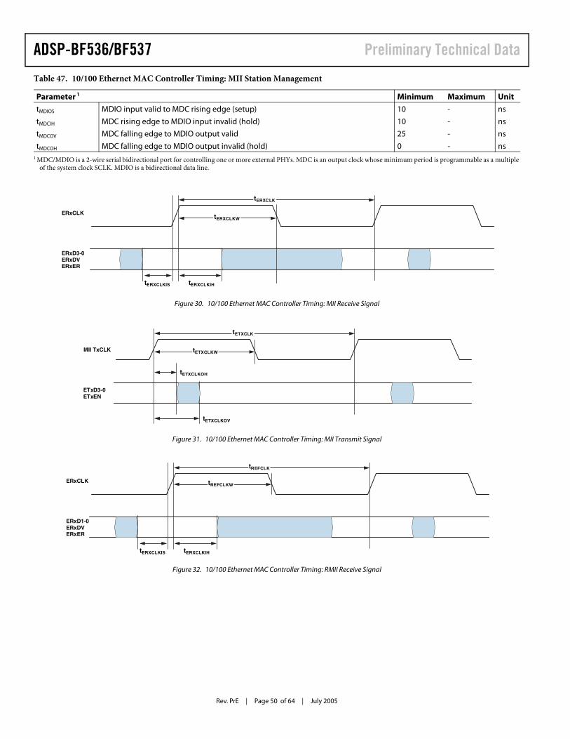
Rev. PrE | Page 50 of 64 | July 2005
ADSP-BF536/BF537 Preliminary Technical Data
Table 47. 10/100 Ethernet MAC Controller Timing: MII Station Management
Parameter 1 Minimum Maximum Unit
tMDIOS MDIO input valid to MDC rising edge (setup) 10 - ns
tMDCIH MDC rising edge to MDIO input invalid (hold) 10 - ns
tMDCOV MDC falling edge to MDIO output valid 25 - ns
tMDCOH MDC falling edge to MDIO output invalid (hold) 0 - ns1 MDC/MDIO is a 2-wire serial bidirectional port for controlling one or more external PHYs. MDC is an output clock whose minimum period is programmable as a multiple
of the system clock SCLK. MDIO is a bidirectional data line.
Figure 30. 10/100 Ethernet MAC Controller Timing: MII Receive Signal
Figure 31. 10/100 Ethernet MAC Controller Timing: MII Transmit Signal
Figure 32. 10/100 Ethernet MAC Controller Timing: RMII Receive Signal
ERxD3-0ERxDVERxER
ERxCLK
tERXCLK
tERXCLKIS tERXCLKIH
tERXCLKW
ETxD3-0ETxEN
MII TxCLK
tETXCLK
tETXCLKOH
tETXCLKOV
tETXCLKW
ERxD1-0ERxDVERxER
ERxCLK
tREFCLK
tERXCLKIS tERXCLKIH
tREFCLKW

ADSP-BF536/BF537Preliminary Technical Data
Rev. PrE | Page 51 of 64 | July 2005
Figure 33. 10/100 Ethernet MAC Controller Timing: RMII Transmit Signal
Figure 34. 10/100 Ethernet MAC Controller Timing: Asynchronous Signal
Figure 35. 10/100 Ethernet MAC Controller Timing: MII Station Management
ETxD1-0ETxEN
RMII REF_CLK
tREFCLK
tEREFCLKOH
tEREFCLKOV
MII CRS, COL
tECRSH tECRSL
tECOLH tECOLL
MDIO (OUTPUT)
MDC (OUTPUT)
tMDCOH
tMDIOS tMDCIH
MDIO (INPUT)
tMDCOV
Rev. PrE | Page 52 of 64 | July 2005
ADSP-BF536/BF537 Preliminary Technical Data
OUTPUT DRIVE CURRENTS
Figure 36 through Figure 45 show typical current-voltage char-acteristics for the output drivers of the ADSP-BF536/BF537 processor. The curves represent the current drive capability of the output drivers as a function of output voltage. See Table 9 on page 19 for information about which driver type corresponds to a particular pin.
Figure 36. Drive Current A (Low VDDEXT)
Figure 37. Drive Current A (High VDDEXT)
SO
UR
CE
CU
RR
EN
T(m
A)
SOURCE VOLTAGE (V)
150
100
50
0
–50
–100
–1500 0.5 1.0 1.5 2.0 2.5 3.0
TBD
SO
UR
CE
CU
RR
EN
T(m
A)
SOURCE VOLTAGE (V)
150
100
50
0
–50
–100
–1500 0.5 1.0 1.5 2.0 2.5 3.0
TBD
Figure 38. Drive Current B (Low VDDEXT)
Figure 39. Drive Current B (High VDDEXT)
SO
UR
CE
CU
RR
EN
T(m
A)
SOURCE VOLTAGE (V)
150
100
50
0
–50
–100
–1500 0.5 1.0 1.5 2.0 2.5 3.0
TBD
SO
UR
CE
CU
RR
EN
T(m
A)
SOURCE VOLTAGE (V)
150
100
50
0
–50
–100
–1500 0.5 1.0 1.5 2.0 2.5 3.0
TBD

ADSP-BF536/BF537Preliminary Technical Data
Rev. PrE | Page 53 of 64 | July 2005
Figure 40. Drive Current C (Low VDDEXT)
Figure 41. Drive Current C (High VDDEXT)
SO
UR
CE
CU
RR
EN
T(m
A)
SOURCE VOLTAGE (V)
150
100
50
0
–50
–100
–1500 0.5 1.0 1.5 2.0 2.5 3.0
TBD
SO
UR
CE
CU
RR
EN
T(m
A)
SOURCE VOLTAGE (V)
150
100
50
0
–50
–100
–1500 0.5 1.0 1.5 2.0 2.5 3.0
TBD
Figure 42. Drive Current D (Low VDDEXT)
Figure 43. Drive Current D (High VDDEXT)
SO
UR
CE
CU
RR
EN
T(m
A)
SOURCE VOLTAGE (V)
150
100
50
0
–50
–100
–1500 0.5 1.0 1.5 2.0 2.5 3.0
TBD
SO
UR
CE
CU
RR
EN
T(m
A)
SOURCE VOLTAGE (V)
150
100
50
0
–50
–100
–1500 0.5 1.0 1.5 2.0 2.5 3.0
TBD

Rev. PrE | Page 54 of 64 | July 2005
ADSP-BF536/BF537 Preliminary Technical Data
Figure 44. Drive Current E (Low VDDEXT)
Figure 45. Drive Current E (High VDDEXT)
SO
UR
CE
CU
RR
EN
T(m
A)
SOURCE VOLTAGE (V)
150
100
50
0
–50
–100
–1500 0.5 1.0 1.5 2.0 2.5 3.0
TBD
SO
UR
CE
CU
RR
EN
T(m
A)
SOURCE VOLTAGE (V)
150
100
50
0
–50
–100
–1500 0.5 1.0 1.5 2.0 2.5 3.0
TBD
ADSP-BF536/BF537Preliminary Technical Data
Rev. PrE | Page 55 of 64 | July 2005
POWER DISSIPATION
Total power dissipation has two components: one due to inter-nal circuitry (PINT) and one due to the switching of external output drivers (PEXT). Table 48 shows the power dissipation for internal circuitry (VDDINT). Internal power dissipation is depen-dent on the instruction execution sequence and the data operands involved. The external component of total power dissipation is caused by the switching of output pins. Its magnitude depends on:
• Maximum frequency (f0) at which all output pins can switch during each cycle
• Load capacitance (C0) of all switching output pins• Their voltage swing (VDDEXT)
The external component is calculated using:
The frequency f includes driving the load high and then back low. For example: DATA15–0 pins can drive high and low at a maximum rate of 1/(2� tSCLK) while in SDRAM burst mode.A typical power consumption can now be calculated for these conditions by adding a typical internal power dissipation:
Note that the conditions causing a worst-case PEXT differ from those causing a worst-case PINT. Maximum PINT cannot occur while 100% of the output pins are switching from all ones (1s) to all zeros (0s). Note, as well, that it is not common for an applica-tion to have 100% or even 50% of the outputs switching simultaneously.
TEST CONDITIONS
All timing parameters appearing in this data sheet were mea-sured under the conditions described in this section.
Output Enable Time
Output pins are considered to be enabled when they have made a transition from a high impedance state to the point when they start driving. The output enable time tENA is the interval from the point when a reference signal reaches a high or low voltage level to the point when the output starts driving as shown in the Output Enable/Disable diagram (Figure 46). The time tENA_MEASURED is the interval from when the reference signal switches to when the output voltage reaches 2.0 V (output high) or 1.0 V (output low). Time tTRIP is the interval from when the output starts driving to when the output reaches the 1.0 V or 2.0 V trip voltage. Time tENA is calculated as shown in the equation:
If multiple pins (such as the data bus) are enabled, the measure-ment value is that of the first pin to start driving.
Output Disable Time
Output pins are considered to be disabled when they stop driv-ing, go into a high impedance state, and start to decay from their output high or low voltage. The time for the voltage on the bus to decay by ∆V is dependent on the capacitive load, CL and the load current, IL. This decay time can be approximated by the equation:
The output disable time tDIS is the difference between tDIS_MEASURED and tDECAY as shown in Figure 46. The time tDIS_MEASURED is the interval from when the reference signal switches to when the output voltage decays ∆V from the mea-sured output high or output low voltage. The time tDECAY is calculated with test loads CL and IL, and with ∆V equal to 0.5 V.
Table 48. Internal Power Dissipation
Test Conditions1
1 IDD data is specified for typical process parameters. All data at 25ºC.
Parameter fCCLK = 50 MHzVDDINT =0.8 V
fCCLK = 150 MHzVDDINT =0.9 V
fCCLK = 250 MHzVDDINT =1.0 V
fCCLK = 400 MHzVDDINT =1.2 V
Unit
IDDTYP2
2 Processor executing 75% dual Mac, 25% ADD with moderate data bus activity.
TBD TBD TBD TBD mA
IDDEFR3
3 Implementation of Enhanced Full Rate (EFR) GSM algorithm.
TBD TBD TBD TBD mA
IDDSLEEP45
4 See the ADSP-BF537 Blackfin Processor Hardware Reference Manual for defini-tions of Sleep and Deep Sleep operating modes.
5 IDDHIBERNATE is measured @ VDDEXT = 3.65 V with VR off (VDDCORE = 0 V).
TBD TBD TBD TBD mA
IDDDEEPSLEEP4 TBD TBD TBD TBD mA
IDDHIBERNATE5 50 50 50 50 µA
Parameter fCCLK = 200 MHzVDDINT =0.9 V
fCCLK = 400 MHzVDDINT =1.0 V
fCCLK = 500 MHzVDDINT =1.2 V
Unit
IDDTYP2 - TBD TBD TBD mA
IDDEFR3 - TBD TBD TBD mA
IDDSLEEP45 - TBD TBD TBD mA
IDDDEEPSLEEP4 - TBD TBD TBD mA
IDDHIBERNATE5 - 50 50 50 µA
Parameter fCCLK = 600 MHzVDDINT =1.2 V
Unit
IDDTYP2 - - - TBD mA
IDDEFR3 - - - TBD mA
IDDSLEEP45 - - - TBD mA
IDDDEEPSLEEP4 - - - TBD mA
IDDHIBERNATE5 - - - 50 µA
PEXT VDDEXT2 C0 f0⋅∑×=
PTOTAL PEXT IDD VDDINT×( )+=
tENA tENA_MEASURED tTRIP–=
tDECAY CL V∆( ) IL⁄=

Rev. PrE | Page 56 of 64 | July 2005
ADSP-BF536/BF537 Preliminary Technical Data
Example System Hold Time Calculation
To determine the data output hold time in a particular system, first calculate tDECAY using the equation given above. Choose ∆V to be the difference between the ADSP-BF536/BF537 proces-sor’s output voltage and the input threshold for the device
requiring the hold time. A typical ∆V will be 0.4 V. CL is the total bus capacitance (per data line), and IL is the total leakage or three-state current (per data line). The hold time will be tDECAY plus the minimum disable time (for example, tDSDAT for an SDRAM write cycle).
ENVIRONMENTAL CONDITIONS
To determine the junction temperature on the application printed circuit board use:
where:TJ = Junction temperature (�C)TCASE = Case temperature (�C) measured by customer at top center of package.ΨJT = From Table 49PD = Power dissipation (see Power Dissipation on Page 55 for the method to calculate PD)Values of θJA are provided for package comparison and printed circuit board design considerations. θJA can be used for a first order approximation of TJ by the equation:
where:TA = Ambient temperature (�C)Values of θJC are provided for package comparison and printed circuit board design considerations when an external heatsink is required.Values of θJB are provided for package comparison and printed circuit board design considerations.
In Table 49, airflow measurements comply with JEDEC stan-dards JESD51-2 and JESD51-6, and the junction-to-board measurement complies with JESD51-8. The junction-to-case measurement complies with MIL-STD-883 (Method 1012.1). All measurements use a 2S2P JEDEC test board.
Figure 46. Output Enable/Disable
REFERENCESIGNAL
tDIS
OUTPUT STARTS DRIVING
VOH (MEASURED) � �V
VOL (MEASURED) + �V
tDIS_MEASURED
VOH
(MEASURED)
VOL
(MEASURED)
2.0V
1.0V
VOH(MEASURED)
VOL
(MEASURED)
HIGH IMPEDANCE STATE.TEST CONDITIONS CAUSE THIS
VOLTAGE TO BE APPROXIMATELY 1.5V.
OUTPUT STOPS DRIVING
tENA
tDECAY
tENA-MEASURED
tTRIP
Figure 47. Equivalent Device Loading for AC Measurements (Includes All Fixtures)
Figure 48. Voltage Reference Levels for AC Measurements (Except Output Enable/Disable)
1.5V
30pF
TOOUTPUT
PIN
50�
INPUTOR
OUTPUT1.5V 1.5V
TJ TCASE ΨJT PD×( )+=
TJ TA θJA PD×( )+=
Table 49. Thermal Characteristics
Parameter Condition Typical Unit
θJA 0 linear m/s air flow �C/W
θJMA 1 linear m/s air flow �C/W
θJMA 2 linear m/s air flow �C/W
θJB �C/W
θJC �C/W
ΨJT 0 linear m/s air flow �C/W

ADSP-BF536/BF537Preliminary Technical Data
Rev. PrE | Page 57 of 64 | July 2005
182-BALL MINI-BGA PINOUTTable 50 lists the mini-BGA pinout by signal mnemonic. Table 51 on Page 58 lists the mini-BGA pinout by ball number.
Table 50. 182-Ball Mini-BGA Ball Assignment (Alphabetically by Signal Mnemonic)
Mnemonic Ball no. Mnemonic Ball no. Mnemonic Ball no. Mnemonic Ball no. Mnemonic Ball no.
ABE0 H13 CLKOUT B14 GND L6 PG8 E3 SRAS D13
ABE1 H12 DATA0 M9 GND L8 PG9 E4 SWE D12
ADDR1 J14 DATA1 N9 GND L10 PH0 C2 TCK P2
ADDR10 M13 DATA10 N6 GND M4 PH1 C3 TDI M3
ADDR11 M14 DATA11 P6 GND M10 PH10 B6 TDO N3
ADDR12 N14 DATA12 M5 GND P14 PH11 A2 TMS N2
ADDR13 N13 DATA13 N5 NMI B10 PH12 A3 TRST N1
ADDR14 N12 DATA14 P5 PF0 M1 PH13 A4 VDDEXT A1
ADDR15 M11 DATA15 P4 PF1 L1 PH14 A5 VDDEXT C12
ADDR16 N11 DATA2 P9 PF10 J2 PH15 A6 VDDEXT E6
ADDR17 P13 DATA3 M8 PF11 J3 PH2 C4 VDDEXT E11
ADDR18 P12 DATA4 N8 PF12 H1 PH3 C5 VDDEXT F4
ADDR19 P11 DATA5 P8 PF13 H2 PH4 C6 VDDEXT F12
ADDR2 K14 DATA6 M7 PF14 H3 PH5 B1 VDDEXT H5
ADDR3 L14 DATA7 N7 PF15 H4 PH6 B2 VDDEXT H10
ADDR4 J13 DATA8 P7 PF2 L2 PH7 B3 VDDEXT J11
ADDR5 K13 DATA9 M6 PF3 L3 PH8 B4 VDDEXT J12
ADDR6 L13 EMU M2 PF4 L4 PH9 B5 VDDEXT K7
ADDR7 K12 GND A10 PF5 K1 PJ0 C7 VDDEXT K9
ADDR8 L12 GND A14 PF6 K2 PJ1 B7 VDDEXT L7
ADDR9 M12 GND D4 PF7 K3 PJ10 D10 VDDEXT L9
AMS0 E14 GND E7 PF8 K4 PJ11 D11 VDDEXT L11
AMS1 F14 GND E9 PF9 J1 PJ2 B11 VDDEXT P1
AMS2 F13 GND F5 PG0 G1 PJ3 C11 VDDINT E5
AMS3 G12 GND F6 PG1 G2 PJ4 D7 VDDINT E8
AOE G13 GND F10 PG10 D1 PJ5 D8 VDDINT E10
ARDY E13 GND F11 PG11 D2 PJ6 C8 VDDINT G10
ARE G14 GND G4 PG12 D3 PJ7 B8 VDDINT K5
AWE H14 GND G5 PG13 D5 PJ8 D9 VDDINT K8
BG P10 GND G11 PG14 D6 PJ9 C9 VDDINT K10
BGH N10 GND H11 PG15 C1 RESET C10 VDDRTC B9
BMODE0 N4 GND J4 PG2 G3 RTXO A8 VROUT0 A13
BMODE1 P3 GND J5 PG3 F1 RTXI A9 VROUT1 B12
BMODE2 L5 GND J9 PG4 F2 SA10 E12 XTAL A11
BR D14 GND J10 PG5 F3 SCAS C14
CLKBUF A7 GND K6 PG6 E1 SCKE B13
CLKIN A12 GND K11 PG7 E2 SMS C13

Rev. PrE | Page 58 of 64 | July 2005
ADSP-BF536/BF537 Preliminary Technical Data
Table 51 lists the mini-BGA pinout by ball number. Table 50 on Page 57 lists the mini-BGA pinout by signal mnemonic.
Table 51. 182-Ball Mini-BGA Ball Assignment (Numerically by Ball Number)
Ball no. Mnemonic Ball no. Mnemonic Ball no. Mnemonic Ball no. Mnemonic Ball no. Mnemonic
A1 VDDEXT C10 RESET F5 GND J14 ADDR1 M9 DATA0
A2 PH11 C11 PJ3 F6 GND K1 PF5 M10 GND
A3 PH12 C12 VDDEXT F10 GND K2 PF6 M11 ADDR15
A4 PH13 C13 SMS F11 GND K3 PF7 M12 ADDR9
A5 PH14 C14 SCAS F12 VDDEXT K4 PF8 M13 ADDR10
A6 PH15 D1 PG10 F13 AMS2 K5 VDDINT M14 ADDR11
A7 CLKBUF D2 PG11 F14 AMS1 K6 GND N1 TRST
A8 RTXO D3 PG12 G1 PG0 K7 VDDEXT N2 TMS
A9 RTXI D4 GND G2 PG1 K8 VDDINT N3 TDO
A10 GND D5 PG13 G3 PG2 K9 VDDEXT N4 BMODE0
A11 XTAL D6 PG14 G4 GND K10 VDDINT N5 DATA13
A12 CLKIN D7 PJ4 G5 GND K11 GND N6 DATA10
A13 VROUT0 D8 PJ5 G10 VDDINT K12 ADDR7 N7 DATA7
A14 GND D9 PJ8 G11 GND K13 ADDR5 N8 DATA4
B1 PH5 D10 PJ10 G12 AMS3 K14 ADDR2 N9 DATA1
B2 PH6 D11 PJ11 G13 AOE L1 PF1 N10 BGH
B3 PH7 D12 SWE G14 ARE L2 PF2 N11 ADDR16
B4 PH8 D13 SRAS H1 PF12 L3 PF3 N12 ADDR14
B5 PH9 D14 BR H2 PF13 L4 PF4 N13 ADDR13
B6 PH10 E1 PG6 H3 PF14 L5 BMODE2 N14 ADDR12
B7 PJ1 E2 PG7 H4 PF15 L6 GND P1 VDDEXT
B8 PJ7 E3 PG8 H5 VDDEXT L7 VDDEXT P2 TCK
B9 VDDRTC E4 PG9 H10 VDDEXT L8 GND P3 BMODE1
B10 NMI E5 VDDINT H11 GND L9 VDDEXT P4 DATA15
B11 PJ2 E6 VDDEXT H12 ABE1 L10 GND P5 DATA14
B12 VROUT1 E7 GND H13 ABE0 L11 VDDEXT P6 DATA11
B13 SCKE E8 VDDINT H14 AWE L12 ADDR8 P7 DATA8
B14 CLKOUT E9 GND J1 PF9 L13 ADDR6 P8 DATA5
C1 PG15 E10 VDDINT J2 PF10 L14 ADDR3 P9 DATA2
C2 PH0 E11 VDDEXT J3 PF11 M1 PF0 P10 BG
C3 PH1 E12 SA10 J4 GND M2 EMU P11 ADDR19
C4 PH2 E13 ARDY J5 GND M3 TDI P12 ADDR18
C5 PH3 E14 AMS0 J9 GND M4 GND P13 ADDR17
C6 PH4 F1 PG3 J10 GND M5 DATA12 P14 GND
C7 PJ0 F2 PG4 J11 VDDEXT M6 DATA9
C8 PJ6 F3 PG5 J12 VDDEXT M7 DATA6
C9 PJ9 F4 VDDEXT J13 ADDR4 M8 DATA3
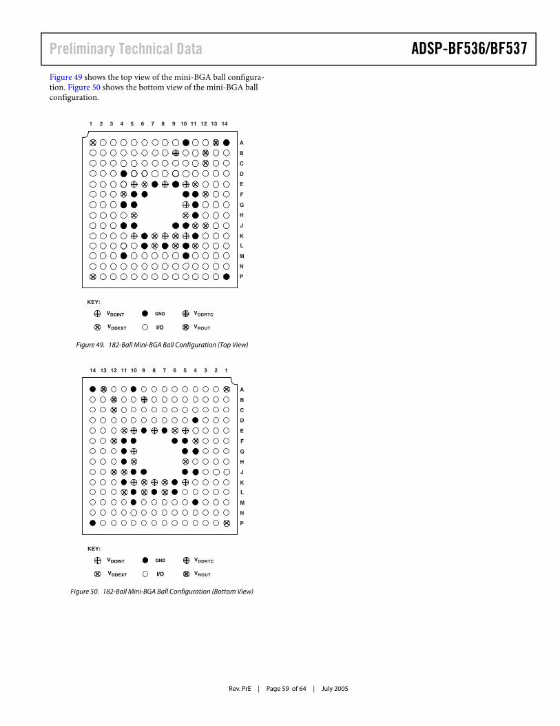
ADSP-BF536/BF537Preliminary Technical Data
Rev. PrE | Page 59 of 64 | July 2005
Figure 49 shows the top view of the mini-BGA ball configura-tion. Figure 50 shows the bottom view of the mini-BGA ball configuration.
Figure 49. 182-Ball Mini-BGA Ball Configuration (Top View)
Figure 50. 182-Ball Mini-BGA Ball Configuration (Bottom View)
A
B
C
D
E
F
G
H
J
K
L
M
N
P
1 2 3 4 5 6 7 8 9 10 11 12 13 14
VDDINT
VDDEXT
GND
I/O
KEY:
VROUT
VDDRTC
A
B
C
D
E
F
G
H
J
K
L
M
N
P
1234567891011121314
VDDINT
VDDEXT
GND
I/O
KEY:
VROUT
VDDRTC
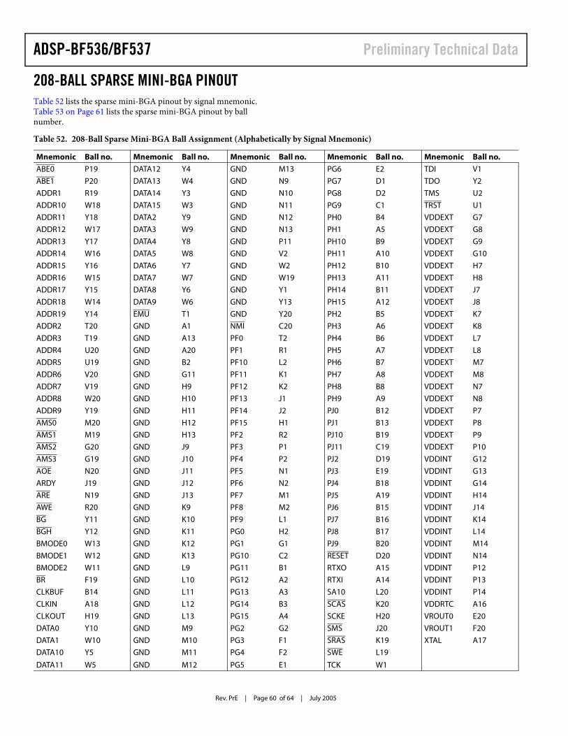
Rev. PrE | Page 60 of 64 | July 2005
ADSP-BF536/BF537 Preliminary Technical Data
208-BALL SPARSE MINI-BGA PINOUTTable 52 lists the sparse mini-BGA pinout by signal mnemonic. Table 53 on Page 61 lists the sparse mini-BGA pinout by ball number.
Table 52. 208-Ball Sparse Mini-BGA Ball Assignment (Alphabetically by Signal Mnemonic)
Mnemonic Ball no. Mnemonic Ball no. Mnemonic Ball no. Mnemonic Ball no. Mnemonic Ball no.
ABE0 P19 DATA12 Y4 GND M13 PG6 E2 TDI V1
ABE1 P20 DATA13 W4 GND N9 PG7 D1 TDO Y2
ADDR1 R19 DATA14 Y3 GND N10 PG8 D2 TMS U2
ADDR10 W18 DATA15 W3 GND N11 PG9 C1 TRST U1
ADDR11 Y18 DATA2 Y9 GND N12 PH0 B4 VDDEXT G7
ADDR12 W17 DATA3 W9 GND N13 PH1 A5 VDDEXT G8
ADDR13 Y17 DATA4 Y8 GND P11 PH10 B9 VDDEXT G9
ADDR14 W16 DATA5 W8 GND V2 PH11 A10 VDDEXT G10
ADDR15 Y16 DATA6 Y7 GND W2 PH12 B10 VDDEXT H7
ADDR16 W15 DATA7 W7 GND W19 PH13 A11 VDDEXT H8
ADDR17 Y15 DATA8 Y6 GND Y1 PH14 B11 VDDEXT J7
ADDR18 W14 DATA9 W6 GND Y13 PH15 A12 VDDEXT J8
ADDR19 Y14 EMU T1 GND Y20 PH2 B5 VDDEXT K7
ADDR2 T20 GND A1 NMI C20 PH3 A6 VDDEXT K8
ADDR3 T19 GND A13 PF0 T2 PH4 B6 VDDEXT L7
ADDR4 U20 GND A20 PF1 R1 PH5 A7 VDDEXT L8
ADDR5 U19 GND B2 PF10 L2 PH6 B7 VDDEXT M7
ADDR6 V20 GND G11 PF11 K1 PH7 A8 VDDEXT M8
ADDR7 V19 GND H9 PF12 K2 PH8 B8 VDDEXT N7
ADDR8 W20 GND H10 PF13 J1 PH9 A9 VDDEXT N8
ADDR9 Y19 GND H11 PF14 J2 PJ0 B12 VDDEXT P7
AMS0 M20 GND H12 PF15 H1 PJ1 B13 VDDEXT P8
AMS1 M19 GND H13 PF2 R2 PJ10 B19 VDDEXT P9
AMS2 G20 GND J9 PF3 P1 PJ11 C19 VDDEXT P10
AMS3 G19 GND J10 PF4 P2 PJ2 D19 VDDINT G12
AOE N20 GND J11 PF5 N1 PJ3 E19 VDDINT G13
ARDY J19 GND J12 PF6 N2 PJ4 B18 VDDINT G14
ARE N19 GND J13 PF7 M1 PJ5 A19 VDDINT H14
AWE R20 GND K9 PF8 M2 PJ6 B15 VDDINT J14
BG Y11 GND K10 PF9 L1 PJ7 B16 VDDINT K14
BGH Y12 GND K11 PG0 H2 PJ8 B17 VDDINT L14
BMODE0 W13 GND K12 PG1 G1 PJ9 B20 VDDINT M14
BMODE1 W12 GND K13 PG10 C2 RESET D20 VDDINT N14
BMODE2 W11 GND L9 PG11 B1 RTXO A15 VDDINT P12
BR F19 GND L10 PG12 A2 RTXI A14 VDDINT P13
CLKBUF B14 GND L11 PG13 A3 SA10 L20 VDDINT P14
CLKIN A18 GND L12 PG14 B3 SCAS K20 VDDRTC A16
CLKOUT H19 GND L13 PG15 A4 SCKE H20 VROUT0 E20
DATA0 Y10 GND M9 PG2 G2 SMS J20 VROUT1 F20
DATA1 W10 GND M10 PG3 F1 SRAS K19 XTAL A17
DATA10 Y5 GND M11 PG4 F2 SWE L19
DATA11 W5 GND M12 PG5 E1 TCK W1
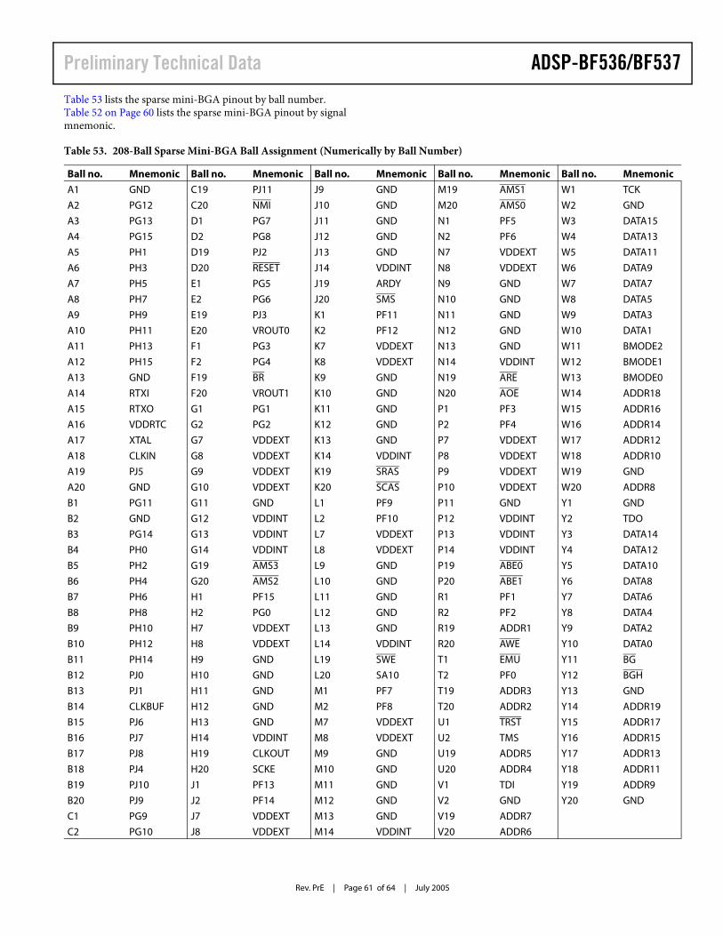
ADSP-BF536/BF537Preliminary Technical Data
Rev. PrE | Page 61 of 64 | July 2005
Table 53 lists the sparse mini-BGA pinout by ball number. Table 52 on Page 60 lists the sparse mini-BGA pinout by signal mnemonic.
Table 53. 208-Ball Sparse Mini-BGA Ball Assignment (Numerically by Ball Number)
Ball no. Mnemonic Ball no. Mnemonic Ball no. Mnemonic Ball no. Mnemonic Ball no. Mnemonic
A1 GND C19 PJ11 J9 GND M19 AMS1 W1 TCK
A2 PG12 C20 NMI J10 GND M20 AMS0 W2 GND
A3 PG13 D1 PG7 J11 GND N1 PF5 W3 DATA15
A4 PG15 D2 PG8 J12 GND N2 PF6 W4 DATA13
A5 PH1 D19 PJ2 J13 GND N7 VDDEXT W5 DATA11
A6 PH3 D20 RESET J14 VDDINT N8 VDDEXT W6 DATA9
A7 PH5 E1 PG5 J19 ARDY N9 GND W7 DATA7
A8 PH7 E2 PG6 J20 SMS N10 GND W8 DATA5
A9 PH9 E19 PJ3 K1 PF11 N11 GND W9 DATA3
A10 PH11 E20 VROUT0 K2 PF12 N12 GND W10 DATA1
A11 PH13 F1 PG3 K7 VDDEXT N13 GND W11 BMODE2
A12 PH15 F2 PG4 K8 VDDEXT N14 VDDINT W12 BMODE1
A13 GND F19 BR K9 GND N19 ARE W13 BMODE0
A14 RTXI F20 VROUT1 K10 GND N20 AOE W14 ADDR18
A15 RTXO G1 PG1 K11 GND P1 PF3 W15 ADDR16
A16 VDDRTC G2 PG2 K12 GND P2 PF4 W16 ADDR14
A17 XTAL G7 VDDEXT K13 GND P7 VDDEXT W17 ADDR12
A18 CLKIN G8 VDDEXT K14 VDDINT P8 VDDEXT W18 ADDR10
A19 PJ5 G9 VDDEXT K19 SRAS P9 VDDEXT W19 GND
A20 GND G10 VDDEXT K20 SCAS P10 VDDEXT W20 ADDR8
B1 PG11 G11 GND L1 PF9 P11 GND Y1 GND
B2 GND G12 VDDINT L2 PF10 P12 VDDINT Y2 TDO
B3 PG14 G13 VDDINT L7 VDDEXT P13 VDDINT Y3 DATA14
B4 PH0 G14 VDDINT L8 VDDEXT P14 VDDINT Y4 DATA12
B5 PH2 G19 AMS3 L9 GND P19 ABE0 Y5 DATA10
B6 PH4 G20 AMS2 L10 GND P20 ABE1 Y6 DATA8
B7 PH6 H1 PF15 L11 GND R1 PF1 Y7 DATA6
B8 PH8 H2 PG0 L12 GND R2 PF2 Y8 DATA4
B9 PH10 H7 VDDEXT L13 GND R19 ADDR1 Y9 DATA2
B10 PH12 H8 VDDEXT L14 VDDINT R20 AWE Y10 DATA0
B11 PH14 H9 GND L19 SWE T1 EMU Y11 BG
B12 PJ0 H10 GND L20 SA10 T2 PF0 Y12 BGH
B13 PJ1 H11 GND M1 PF7 T19 ADDR3 Y13 GND
B14 CLKBUF H12 GND M2 PF8 T20 ADDR2 Y14 ADDR19
B15 PJ6 H13 GND M7 VDDEXT U1 TRST Y15 ADDR17
B16 PJ7 H14 VDDINT M8 VDDEXT U2 TMS Y16 ADDR15
B17 PJ8 H19 CLKOUT M9 GND U19 ADDR5 Y17 ADDR13
B18 PJ4 H20 SCKE M10 GND U20 ADDR4 Y18 ADDR11
B19 PJ10 J1 PF13 M11 GND V1 TDI Y19 ADDR9
B20 PJ9 J2 PF14 M12 GND V2 GND Y20 GND
C1 PG9 J7 VDDEXT M13 GND V19 ADDR7
C2 PG10 J8 VDDEXT M14 VDDINT V20 ADDR6
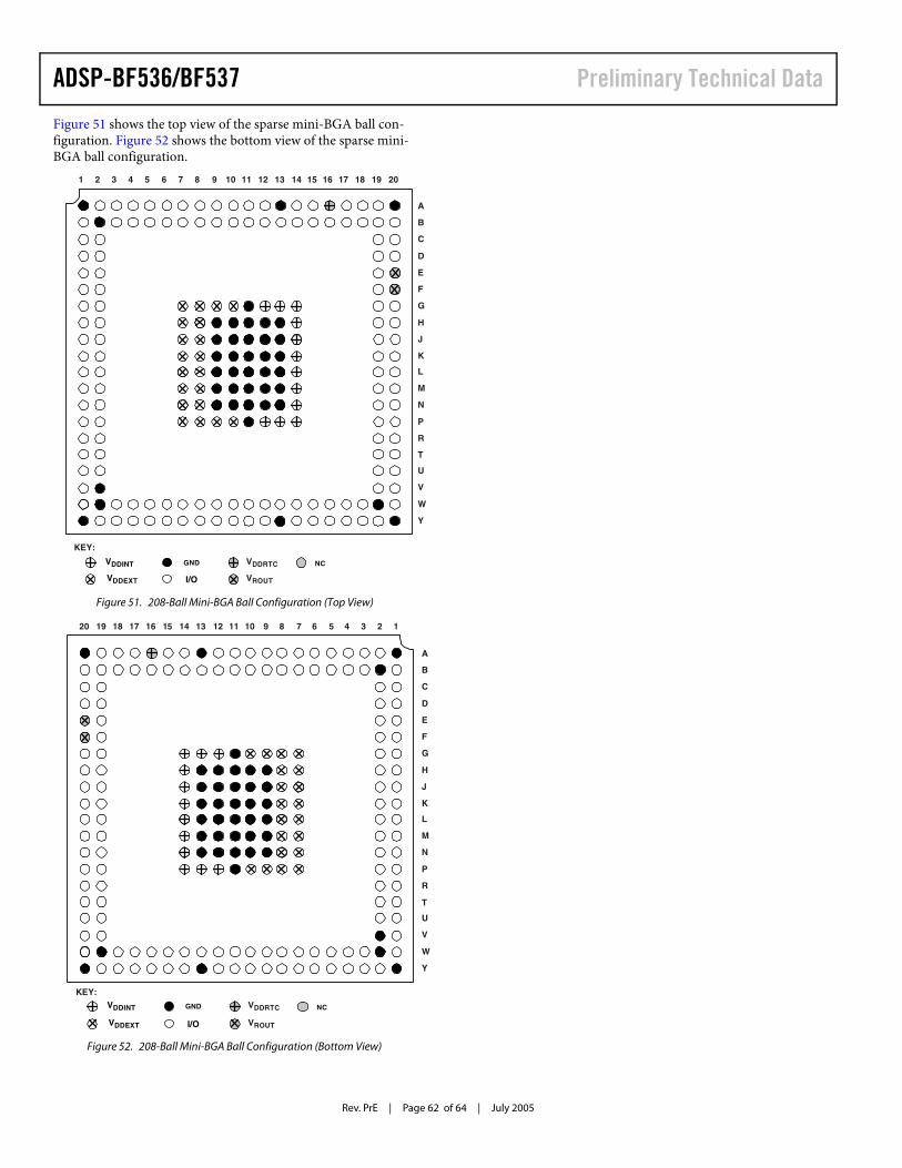
Rev. PrE | Page 62 of 64 | July 2005
ADSP-BF536/BF537 Preliminary Technical Data
Figure 51 shows the top view of the sparse mini-BGA ball con-figuration. Figure 52 shows the bottom view of the sparse mini-BGA ball configuration.
Figure 51. 208-Ball Mini-BGA Ball Configuration (Top View)
Figure 52. 208-Ball Mini-BGA Ball Configuration (Bottom View)
A
B
C
D
E
F
G
H
J
K
L
M
N
P
1 2 3 4 5 6 7 8 9 10 11 12 13 14 16 17 18 19 2015
VDDINT
VDDEXT
GND
I/O
KEY:
VROUT
VDDRTC
R
T
U
V
W
Y
NC
A
B
C
D
E
F
G
H
J
K
L
M
N
P
20 19 18 17 16 15 14 13 12 11 10 9 8 7 5 4 3 2 16
VDDINT
VDDEXT
GND
I/O
KEY:
VROUT
VDDRTC
R
T
U
V
W
Y
NC
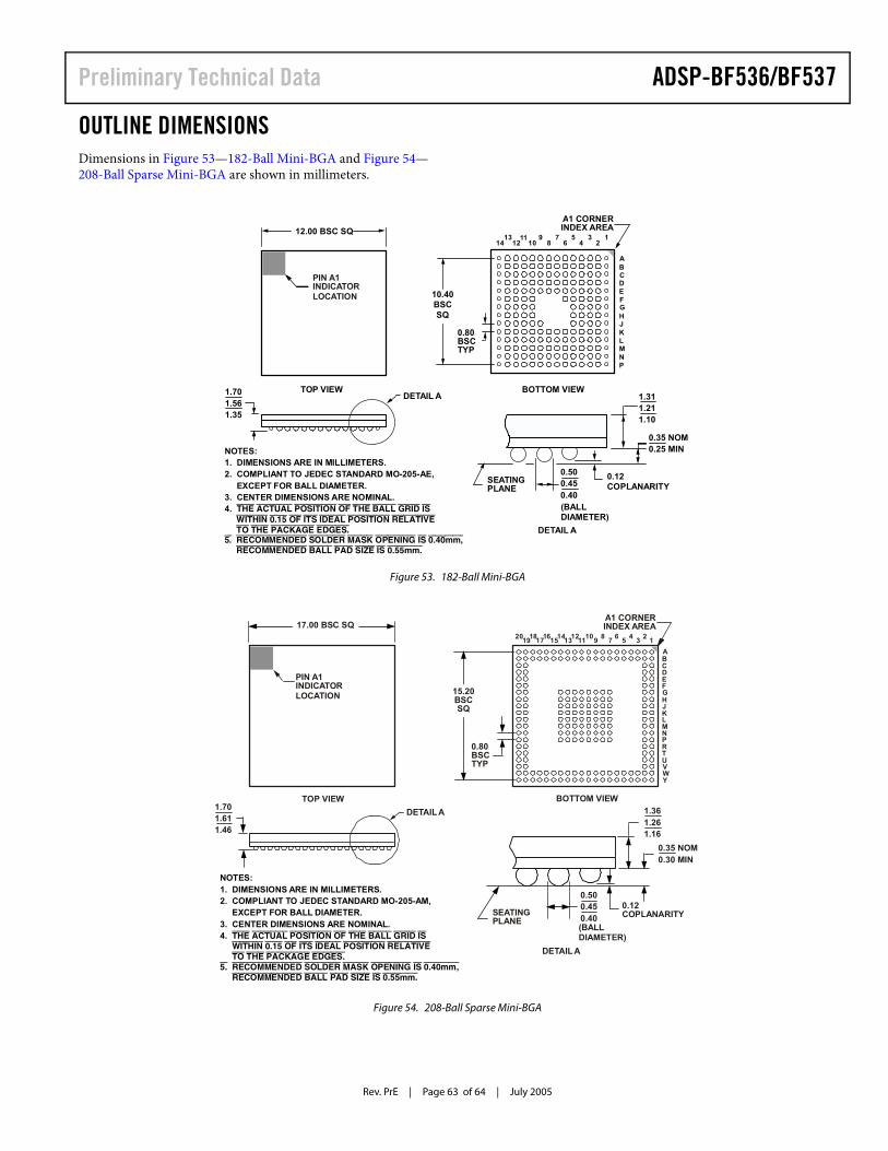
ADSP-BF536/BF537Preliminary Technical Data
Rev. PrE | Page 63 of 64 | July 2005
OUTLINE DIMENSIONSDimensions in Figure 53—182-Ball Mini-BGA and Figure 54—208-Ball Sparse Mini-BGA are shown in millimeters.
Figure 53. 182-Ball Mini-BGA
Figure 54. 208-Ball Sparse Mini-BGA
0.80BSCTYP
DETAIL A
DETAIL A
0.500.450.40
1.311.211.10
10.40BSCSQ
ABCDEFGHJKLMNP
1413121110 8
76
3219 5
4
A1 CORNERINDEX AREA
TOP VIEW BOTTOM VIEW1.701.561.35
12.00 BSC SQ
(BALLDIAMETER)
SEATINGPLANE
0.35 NOM0.25 MIN
0.12COPLANARITY
PIN A1INDICATORLOCATION
NOTES:1. DIMENSIONS ARE IN MILLIMETERS.2. COMPLIANT TO JEDEC STANDARD MO-205-AE,EXCEPT FOR BALL DIAMETER.
3. CENTER DIMENSIONSARE NOMINAL.4. THE ACTUAL POSITION OF THE BALL GRID IS
WITHIN 0.15 OF ITS IDEAL POSITION RELATIVETO THE PACKAGE EDGES.
5. RECOMMENDED SOLDER MASK OPENING IS 0.40mm,RECOMMENDED BALL PAD SIZE IS 0.55mm.
0.80BSCTYP
ABCDEFGHJKLMNPRTUVWY
15141716191820 131211109 8 7 6 5 4 3 2 1
BOTTOM VIEW
15.20BSCSQ
A1 CORNERINDEXAREA
0.12COPLANARITY
DETAILA
0.500.450.40(BALLDIAMETER)
0.35 NOM0.30 MIN
TOP VIEW
PIN A1INDICATORLOCATION
DETAILA
17.00 BSC SQ
SEATINGPLANE
1.701.611.46
1.361.261.16
NOTES:1. DIMENSIONS ARE IN MILLIMETERS.2. COMPLIANT TO JEDEC STANDARD MO-205-AM,EXCEPT FOR BALL DIAMETER.
3. CENTER DIMENSIONS ARE NOMINAL.4. THE ACTUAL POSITION OF THE BALL GRID IS
WITHIN 0.15 OF ITS IDEAL POSITION RELATIVETO THE PACKAGE EDGES.
5. RECOMMENDED SOLDER MASK OPENING IS 0.40mm,RECOMMENDED BALL PAD SIZE IS 0.55mm.
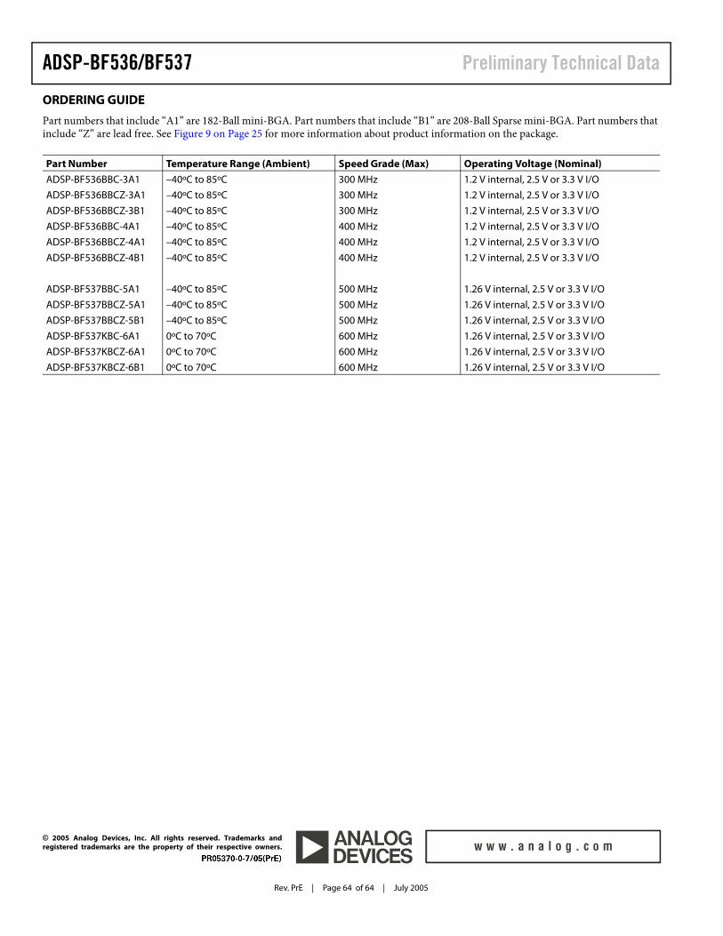
Rev. PrE | Page 64 of 64 | July 2005
ADSP-BF536/BF537 Preliminary Technical Data
© 2005 Analog Devices, Inc. All rights reserved. Trademarks andregistered trademarks are the property of their respective owners.
ORDERING GUIDE
Part numbers that include “A1” are 182-Ball mini-BGA. Part numbers that include “B1” are 208-Ball Sparse mini-BGA. Part numbers that include “Z” are lead free. See Figure 9 on Page 25 for more information about product information on the package.
Part Number Temperature Range (Ambient) Speed Grade (Max) Operating Voltage (Nominal)
ADSP-BF536BBC-3A1 –40ºC to 85ºC 300 MHz 1.2 V internal, 2.5 V or 3.3 V I/O
ADSP-BF536BBCZ-3A1 –40ºC to 85ºC 300 MHz 1.2 V internal, 2.5 V or 3.3 V I/O
ADSP-BF536BBCZ-3B1 –40ºC to 85ºC 300 MHz 1.2 V internal, 2.5 V or 3.3 V I/O
ADSP-BF536BBC-4A1 –40ºC to 85ºC 400 MHz 1.2 V internal, 2.5 V or 3.3 V I/O
ADSP-BF536BBCZ-4A1 –40ºC to 85ºC 400 MHz 1.2 V internal, 2.5 V or 3.3 V I/O
ADSP-BF536BBCZ-4B1 –40ºC to 85ºC 400 MHz 1.2 V internal, 2.5 V or 3.3 V I/O
ADSP-BF537BBC-5A1 –40ºC to 85ºC 500 MHz 1.26 V internal, 2.5 V or 3.3 V I/O
ADSP-BF537BBCZ-5A1 –40ºC to 85ºC 500 MHz 1.26 V internal, 2.5 V or 3.3 V I/O
ADSP-BF537BBCZ-5B1 –40ºC to 85ºC 500 MHz 1.26 V internal, 2.5 V or 3.3 V I/O
ADSP-BF537KBC-6A1 0ºC to 70ºC 600 MHz 1.26 V internal, 2.5 V or 3.3 V I/O
ADSP-BF537KBCZ-6A1 0ºC to 70ºC 600 MHz 1.26 V internal, 2.5 V or 3.3 V I/O
ADSP-BF537KBCZ-6B1 0ºC to 70ºC 600 MHz 1.26 V internal, 2.5 V or 3.3 V I/O