Embed Size (px)
Citation preview
Ab initio study on influence of dopants on crystalline and amorphousGe2Sb2Te5
Eunae Cho,1 Seungwu Han,1,a) Dohyung Kim,2 Hideki Horii,2 and Ho-Seok Nam3
1Department of Materials Science and Engineering, Seoul National University, Seoul 151-744, Korea2Process Development Team, Memory R&D Center, Semiconductor Business, Samsung Electronics,Yongin 446-71, Korea3Center for Materials and Processes of Self-Assembly and School of Advanced Materials Engineering,Kookmin University, Seoul 136-702, Korea
(Received 10 November 2010; accepted 6 January 2011; published online 28 February 2011)
The pronounced effects of dopants such as Si, N, and O atoms, on material properties of
Ge2Sb2Te5 are investigated at the atomic level using ab initio calculations. In the crystalline phase,
stable doping sites are determined by characteristic chemical bonds such as Ge–N and Ge–O. The
comparison of lattice parameters between theory and experiment supports the existence of dopants
at vacant or interstitial positions. The electronic density of states indicate that the localization at the
valence top increases with N- or O-doping, explaining the increase of resistivity in experiments.
The amorphous structures of doped Ge2Sb2Te5 are obtained by melt-quench simulations and they
are well understood by selective bonds between dopants and host atoms. The chemical bonds
around dopants are more favorable in the amorphous phase than in the crystalline state, accounting
for increased amorphous stability of doped Ge2Sb2Te5. The atomic and electronic structures of
amorphous Ge2Sb2Te5 do not support a viewpoint that the bonding nature is changed toward the
covalent character upon doping. The recrystallization of doped Ge2Sb2Te5 is also simulated and it
is directly confirmed that the crystallization process of doped Ge2Sb2Te5 is slowed down by
dopants. VC 2011 American Institute of Physics. [doi:10.1063/1.3553851]
I. INTRODUCTION
Ge2Sb2Te5 (GST) is a representative phase-changing
chalcogenide compound that shows stable and fast phase
transitions between crystalline and amorphous phases. GST
has been actively employed in optical disks such as DVD,
and more recently it is applied to solid state memories such
as the phase-change random access memory (PRAM).1 Even
though undoped GST is already superior to other material
families in many respects, various efforts have been devoted
to tailoring physical properties of GST with an aim to
enhance the device performance further. Among them, a
popular approach is to incorporate small amounts of dopants
such as Si,2–4 N,4–13 and O atoms.10,14 The purpose of doping
slightly varies with application targets; when applied to opti-
cal memories, it was noted that N-doped GST improves the
stability of amorphous marks, as evidenced by the increased
crystallization time.6,8 In PRAM, N-doping provides a con-
venient solution to reduce the electric current required to
transform the crystalline GST into the amorphous phase (so
called reset currents).9 This is because N doping increases
resistivity in the crystalline phase. Similar benefits were also
achieved with Si (Ref. 3) and O (Refs. 10, 14) dopants.
The pronounced effects of dopants have been explained
considering two factors. First, it has been observed that the
dopants tend to reduce the grain size,4,7,8,15 possibly caused
by dopant segregation near grain boundaries in the form of
nitrides or oxides.4,6,16 The resistance of the crystalline phase
would increase due to additional electron scattering from
grain boundaries.9 As a more intrinsic origin, it was also sug-
gested that the dopants affect the bonding character to be
more covalent or induce lattice strain as they take up tetrahe-
dral sites.10 However, these assumptions have not been fully
supported by microscopic evidence and the fundamental
understanding on the role of dopants is still elusive, limiting
efforts to identify optimal dopant species and concentrations.
Theoretically, ab initio molecular dynamics (MD) simula-
tions have provided rich information on amorphous structures
of undoped GST.17–25 It has been consistently demonstrated
that the local order is different between crystalline and amor-
phous GST (a-GST), which accounts for the distinct physical
properties between the two phases.19,24,26 In contrast, there are
few studies on doped GST.16,27,28 In Refs. 16 and 27, N atoms
in a-GST were found to dominantly bond with Ge atoms. The
N dopants in the hexagonal phase were studied in Ref. 28 and
it was found that the N2 molecule was more stable than inter-
stitial N atoms. However, to gain further insights into the
influence of dopants on the crystalline and amorphous GST, a
more systematic study considering both phases is strongly
required. Furthermore, various types of dopants need to be
compared simultaneously to map out the relationship between
the chemical nature of dopants and the change in atomic and
electronic structures, thereby providing guideline to select
optimal dopants. Motivated by this situation, we carry out in
this work extensive ab initio calculations to reveal atomic and
electronic structures of GST doped with Si, N, and O atoms,
which are currently under active investigations. In the present
work, we focus on atomically resolved dopants in the crystal-
line and amorphous GST but it is noted that extrinsic effects
a)Author to whom correspondence should be addressed. Electronic mail:
0021-8979/2011/109(4)/043705/10/$30.00 VC 2011 American Institute of Physics109, 043705-1
JOURNAL OF APPLIED PHYSICS 109, 043705 (2011)
Downloaded 01 Mar 2011 to 147.46.197.64. Redistribution subject to AIP license or copyright; see http://jap.aip.org/about/rights_and_permissions
such as segregation of dopants near grain boundaries may also
play significant roles in real samples.
II. COMPUTATIONAL METHODS
We perform ab initio calculations based on the density
functional theory. The Vienna Ab-initio Simulation Pack-
age29 is used for molecular dynamics simulations and the
electronic structure calculations. The projector-augmented-
wave pseudopotentials30 are used to describe electron-ion
interactions. For the exchange-correlation energies between
electrons, the generalized gradient approximation based on
the Perdew–Burke–Ernzerhof (PBE) functional31 is employed.
The energy cutoff for the plane-wave basis expansion is cho-
sen to be 131, 184, 210, and 220 eV for MD simulations of
undoped, Si-, N-, and O-doped GST, respectively. The higher
energy cutoff of 250 eV is used when the structural relaxation
is performed. The atomic positions are relaxed until the
Hellmann–Feynman force on each atom is reduced to within
0.03 eV/A.
The k points in the first Brillouin zone are sampled dif-
ferently according to the supercell size and computational
mode. In studying dopants in crystalline GST including 72
atoms within the supercell (Sec. III), a 2� 2� 2 regular
mesh is used consistently. When a larger size of 216-atom
supercell is used for studying amorphous phase (Secs. IV A
and IV B), the C point is sampled for MD simulations and
the ensuing structural relaxation is performed with the single
(0.25, 0.25, 0.25) point. In plotting the density of states
(DOS), a 2� 2� 2 regular mesh is used. Finally, the single
(0.25, 0.25, 0.25) point is used in the recrystallization simu-
lation on the 72-atom supercell (Sec. IV C).
III. DOPANTS IN CRYSTALLINE Ge2Sb2Te5
A. Stable doping sites
First, we discuss on stable sites of dopants in crystalline
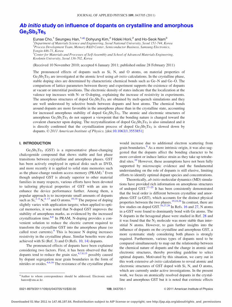
(cubic) GST (c-GST). Figure 1(a) shows five representative
doping types, XGe, XSb, XTe, Xvac, and Xi, where X indicates
one of Si, N, and O atoms. XGe, XSb, and XTe mean the sub-
stitutional doping in which the dopant X replaces Ge, Sb and
Te atoms, respectively. For Xvac, the dopant is placed on an
empty lattice site of c-GST. Finally, a dopant at the interstice
inside the lattice cube is denoted as Xi. Initially, a dopant at
Xi is placed at the lattice-cube center corresponding to the
tetrahedral site, but they relax away from this position signif-
icantly (see below). As the cation sublattice sites (or A sites)
are randomly occupied with Ge, Sb, and vacancies, local
configurations are not unique for a given doping type. To
account for the configurational variation, we randomly select
five sites for each doping type and average the results.
We use a 13.7� 13.7� 12.2 A3 supercell comprising 72
atoms and introduce one dopant atom per supercell. This cor-
responds to a doping concentration of 1.4 at. %. To compare
the relative stability among dopant sites, we calculate the
formation energy (Efor) as follows:
Efor¼EtotðX-doped c-GSTÞ�Etotðundoped c-GSTÞ�lXþl0;
(1)
where Etot is the total energy per supercell with or without
dopants, and lX is the chemical potential of the dopant X.
The last term in Eq. (1), l0, indicates the chemical potential
of Ge, Sb, and Te for XGe, XSb, and XTe, respectively, while
it is zero for Xvac and Xi. The chemical potentials for Si, Ge,
Sb, and Te atoms are set to their total energies in the most
stable crystalline structure. For N and O, half of the total
energy of the diatomic molecule is used as the chemical
potential.
Figure 1(b) displays the computed Efor’s averaged over
five configurations. The standard deviations are denoted by
error bars. The small dopants such as N and O show wider
error bars than Si dopants. This is because N and O form
bonds with mainly Ge or Sb atoms, and therefore more sensi-
tive to A-site variations. For Si, the most stable site is found
to be SiGe. This is because Si atoms are chemically most sim-
ilar to Ge atoms. As such, SiGe gives rise to little lattice
deformations around the dopant site.
In Fig. 1(b), Efor’s for N and O dopants differ by 3–4 eV
even though the two elements are next to each other in the
Periodic Table. The dissociation energies of N2 and O2 mole-
cules are calculated to be 9.53 and 5.61 eV within the present
computational conditions, respectively. [Experimental values
are 9.79 eV (N2) and 5.15 eV (O2).32] Therefore, the large,
positive Efor’s for N dopants mainly originate from the strong
binding energy of N2 molecules. This also excludes a possibil-
ity that N atoms are doped through spontaneous dissociation
of N2 molecules. This result is consistent with other calcula-
tions on N-doped hexagonal GST (Refs. 4 and 28) and also
experimental observations of N2 molecules in N-doped
GST.33 However, ion collisions during the reactive sputtering
FIG. 1. (Color online) (a) Five representative doping sites in the crystalline
Ge2Sb2Te5. (b) The formation energy with respect to the dopant species and
doping sites.
043705-2 Cho et al. J. Appl. Phys. 109, 043705 (2011)
Downloaded 01 Mar 2011 to 147.46.197.64. Redistribution subject to AIP license or copyright; see http://jap.aip.org/about/rights_and_permissions
method, the most favored process to grow doped GST, may
generate atomic nitrogen from N2 molecules which is then
incorporated into the thin film. Furthermore, the similarities
between samples doped by reactive sputtering and ion implan-
tation10 also supports that the atomically resolved nitrogen as
studied in this work may actually be present in significant
amounts and affect various properties of doped GST.
Figure 1(b) shows that N and O atoms favor XTe or Xi
over A-site doping. The N atoms in Te sites move along the
diagonal direction and form three bonds with Ge or Sb
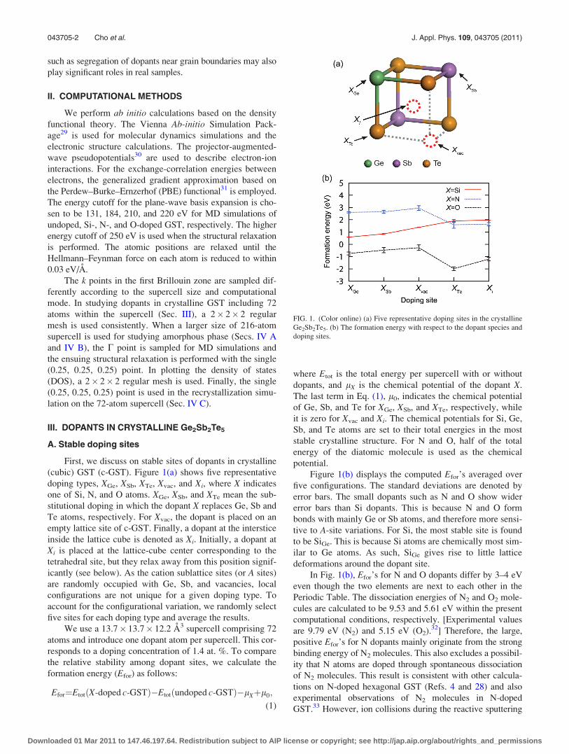
atoms. A typical geometry is presented in Fig. 2(a) which
shows that the N dopant is bonded with three Ge atoms. It is
found that Efor’s among the five statistical samples are
decreased with the increasing number of Ge-N bonds. This
suggests that Ge-N bonds are more stable than Sb-N bonds.
A similar observation is also found for OTe; O dopants shift
away from the original position and form bonds with neigh-
boring Ge atoms. [See Fig. 2(b).] In contrast to predominant
threefold coordination of NTe, most OTe dopants are bivalent.
On the other hand, Ni and Oi dopants typically relax toward
a cube corner (initially they were placed at the tetrahedral
site) and push out nearby Te atoms, thereby establishing
bonds with Ge or Sb atoms [see Figs. 2(c) and 2(d)]. As a
result, the local configurations are similar to those of XTe
except for extra N–Te or O–Te bonds. The large displace-
ment of Te atoms is facilitated by the nearby A-site vacancy.
The preferential Ge–N and Ge–O bonds can be under-
stood based on Pauling’s electronegativities which are 3.04
(N), 3.44 (O), 2.01 (Ge), 2.05 (Sb), and 2.1 (Te). Therefore,
the largest difference in electronegativity results when N and
O dopants establish chemical bonding with Ge atoms. The
stable Ge–N and Ge–O bonds can also be inferred by the ex-
istence of crystalline phases of Ge3N4 and GeO2; for germa-
nium nitrides, the most stable phase is b-Ge3N4 with Ge
atoms in the tetrahedral configuration and N atoms in a
planar, threefold coordination. The average Ge-N bond
length in b-Ge3N4 is 1.85 A from the present calculation. On
the other hand, there are two phases of germania with similar
energies: b-quartz and rutile structures. The two phases dif-
fer in energy by only 0.01 eV per formula unit within the
present calculation. However, the local configurations are
different as (Ge, O) show (4, 2) and (6, 3) coordinations in
b-quartz and rutile structures, respectively. This also results
in distinct Ge-O bond lengths of 1.78 (b-quartz) and 1.89
(rutile) A.
The local structures in Fig. 2 resemble the crystalline
structures of Ge3N4 and GeO2, accounting for the stability of
XTe and Xi. Consistently, the average Ge-XTe or Ge-Xi bond
lengths [2.05 (NTe), 1.98 (OTe), 1.93 (Ni), 1.94 (Oi) A] are
close to the above theoretical bond lengths in crystalline
phases albeit slightly longer. Since these bond lengths are
much shorter than the average nearest-neighbor distance in
c-GST (�3 A), Ge–N and Ge–O bonds give rise to signifi-
cant lattice deformations as visible in Fig. 2. We also note
that the local structure is more favorable for OTe than NTe; in
b-quartz GeO2, the O atom is twofold coordinated with the
Ge–O–Ge angle of 130�. This configuration is closely repro-
duced by OTe in Fig. 2(d). By contrast, N atoms in b-Ge3N4
form a planar bonding with three Ge atoms but the local con-
figuration around NTe in Fig. 2(a) is rather distorted from
this geometry due to the orthogonal p-bonding network in
c-GST. This may contribute in part to the large difference in
Efor between NTe and OTe.
B. Influence of dopants on lattice parameters
The lattice distortion induced by dopants affects lattice
parameters. In order to analyze this quantitatively, we exam-
ine crystal structures at high doping concentrations. In Fig.
3, variations in lattice parameters are computed when 4 or 8
dopants are introduced in each 72-atom supercell with a cer-
tain doping type, which corresponds to concentrations of �5
or �10 at. %, respectively. Both cell shapes and volumes are
optimized in addition to the atomic relaxation. To facilitate
the comparison with experiment, the equilibrium lattice pa-
rameter is set to (Vrelaxed/10)1/3 with Vrelaxed being the final
volume after cell optimization. The lattice parameter for
undoped c-GST is 6.1 A, in good agreement with the experi-
mental value of 5.99 A.
In spite of chemical diversity between studied dopants,
lattice parameters in Fig. 3 show systematic behaviors com-
mon to all dopants. First, all interstitial dopants increase the
lattice parameters, which is certainly a result of positive
strain induced by dopants. The expansion is most pro-
nounced for Sii due to the large atomic size. In contrast, the
most stable SiGe dopants reduce the lattice parameter
because the atomic size of Si is smaller than for Ge. In Ref.
15, the lattice parameters of Si-doped c-GST were measured
with respect to the dopant concentration and they are indi-
cated by empty circles in Fig. 3(a). This expansion is not
explained by SiGe dopants and may indicate the presence of
some amounts of Sivac or Sii. [From the energetic point of
view, Sivac would be more favorable as shown in Fig. 1(b).]
On the other hand, the experimental lattice parameters forFIG. 2. (Color online) Representative local structures around dopants. (a)
NTe, (b) OTe, (c) Ni, and (d) Oi.
043705-3 Cho et al. J. Appl. Phys. 109, 043705 (2011)
Downloaded 01 Mar 2011 to 147.46.197.64. Redistribution subject to AIP license or copyright; see http://jap.aip.org/about/rights_and_permissions

N-doped c-GST are noted in Fig. 3(b) as empty circles.7 This
experimental change is well explained by Ni dopants, sup-
porting that significant amounts of N dopants exist in atomic
states. (However, we also note that some experiment did not
observe noticeable changes in the lattice parameter.4)
Although there is no quantitative analysis, the x-ray diffrac-
tion data on O-doped c-GST in Ref. 14 are consistent with
the increasing lattice parameters, which is also evidence of
the interstitial form of O dopants because no other dopant
types result in the volume expansion. The presence of dop-
ants at interstitial sites, instead of substitutional ones, hints
that dopants do not disturb the original stoichiometry of GST
significantly.
C. Electronic structures of doped crystallineGe2Sb2Te5
To investigate how dopants affect electronic structures
of c-GST, we calculate in Fig. 4 the density of states (DOS)
for 72-atom supercells with 4 dopants at stable doping sites
(�5 at. % doping concentrations). For the comparison pur-
pose, DOS for undoped c-GST is also shown in Fig. 4(a). To
analyze the electron localization, we calculate on the right
scale the inverse participation ratio (IPR) defined as follows:
IPR ¼P
i aij j4P
i aij j2� �2
; (2)
where |ai|2 indicates the partial weight on the ith atom. IPR
provides a convenient way to explore the spatial localization
of a quantum state. For example, if the wave function is uni-
formly distributed over N atoms, IPR is equal to 1/N.
In Fig. 4, SiGe and Ni dopants reduce the energy gap
while OTe dopants increase the gap. To relate electronic
structures to material properties, we calculate optical dielec-
tric constants (e1) using the linear response approach. The
diagonally averaged e1 is shown within each figure. The
increase and decrease in e1 for SiGe and OTe, respectively,
are consistent with the energy-gap variation because the
smaller energy gap facilitates electronic polarization. How-
ever, the experiment in Ref. 14 showed that the refractive
index (or e1) of c-GST was increased with O dopants, which
may imply that the change in macroscopic morphology such
as the grain size would also affect the measured dielectric
constant. In the case of Ni, e1 is reduced in spite of the gap
reduction. This is attributed to the enhanced electronic local-
ization (see below) near valence and conduction edges com-
pared to undoped c-GST since the localized state is less
polarizable due to a large energy separation between bonding
and antibonding states.
FIG. 3. (Color online) The lattice parameters of (a) Si-, (b) N-, and (c) O-
doped crystalline Ge2Sb2Te5 with respect to the doping concentration. In (a)
and (b), experimental data are also provided.
FIG. 4. (Color online) The density of states of c-GST with (a) no dopant,
(b) SiGe, (c) Ni, and (d) OTe. The inverse participation ratios (IPRs) are noted
on the right scale. The computed optical dielectric constants with the diago-
nal average (e1) are shown within each figure.
043705-4 Cho et al. J. Appl. Phys. 109, 043705 (2011)
Downloaded 01 Mar 2011 to 147.46.197.64. Redistribution subject to AIP license or copyright; see http://jap.aip.org/about/rights_and_permissions
The increase of IPR near valence edges in Ni and OTe
means that electrons in this energy range are more localized
than corresponding states in undoped c-GST. From the anal-
ysis on the spatial distribution of wave functions, these states
are found to be distributed over dopant 2p and Te 5p orbitals.
It is well established that c-GST behaves like a p-type semi-
conductor,34 which is attributed to the formation of Ge
vacancies.35 Therefore, the localized states near the valence
edges in Ni and OTe imply that the dopants will play as
strong scattering centers in p-type c-GST. This is consistent
with experiment showing that the resistivity of c-GST
increases with doping.2,9–11 By contrast, the influence of
SiGe dopants on the conductivity of c-GST would be rela-
tively weaker because IPR is very similar to that in undoped
c-GST. In fact, it was observed in Ref. 3 that N-doped
c-GST is more resistive than Si-doped samples with similar
doping concentrations.
IV. DOPANTS IN AMORPHOUS Ge2Sb2Te5
To obtain amorphous structures of doped GST, we carry
out melt-quench MD simulations. The initial crystalline rock
salt structures comprise 216 atoms and 12 dopants are intro-
duced per unit supercell. Initially, Si dopants replace Ge
atoms and N and O atoms are placed at interstitial positions.
The resulting doping concentrations are 5.6 and 5.3 at. % for
Si and N (or O) dopants, respectively. Since the accurate
composition of doped GST is not available experimentally,
the present choice of initial doping types should be regarded
as one of the possibilities. To reflect the density reduction af-
ter amorphization, the supercell volume during melt-quench
simulations is fixed to 7360 A3 which is slightly larger than
6935 A3 for undoped c-GST. As will be shown in the below,
the final amorphous density varies depending on the dopant
species. For melt-quench simulations, the temperature is
increased to 2000 K and the system is melted for 12 ps to
erase crystalline information. The liquid is then cooled to
1000 K and melted for 30 ps additionally. The liquid struc-
ture is subsequently quenched from 1000 to 300 K with a
cooling rate of � 15 K/ps. The final structure is fully relaxed
at 0 K by optimizing lattice parameters and atomic positions.
A. Atomic structures of doped amorphous Ge2Sb2Te5
The computed melt-quenched amorphous structures are
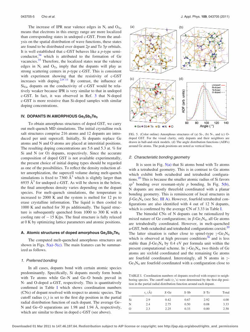
shown in Figs. 5(a)–5(c). The main features can be summar-
ized as follows.
1. Preferred bonding
In all cases, dopants bond with certain atomic species
predominantly. Specifically, Si dopants mostly form bonds
with Te atoms while Ge–N and Ge–O bonds prevail in
N- and O-doped a-GST, respectively. This is quantitatively
confirmed in Table I which shows coordination numbers
(CNs) of dopant resolved with respect to atomic species. The
cutoff radius (rc) is set to the first dip position in the partial
radial distribution function of each dopant. The average Ge–
N and Ge–O separations are 1.98 and 1.94 A, respectively,
which are similar to those in doped c-GST (see above).
2. Characteristic bonding geometry
It is seen in Fig. 5(a) that Si atoms bond with Te atoms
with a tetrahedral geometry. This is in contrast to Ge atoms
which exhibit both octahedral and tetrahedral configura-
tions.20 This is because the smaller atomic radius of Si favors
sp3 bonding over resonant-style p bonding. In Fig. 5(b),
N dopants are mostly threefold coordinated with a planar
bonding geometry. This is reminiscent of local structures in
b-Ge3N4 (see Sec. III A). However, fourfold tetrahedral con-
figurations are also identified with 4 out of 12 N dopants,
which is confirmed by the average CN of 3.33 in Table I.
The bimodal CNs of N dopants can be rationalized by
mixed nature of Ge configurations; in b-Ge3N4, all Ge atoms
are tetrahedrally coordinated. However, in melt-quenched
a-GST, both octahedral and tetrahedral configurations coexist.20
The latter situation is rather close to spinel-type c-Ge3N4
which is observed at high pressure conditions36 and is less
stable than b-Ge3N4 by 0.4 eV per formula unit within the
present computational scheme. In c-Ge3N4, two thirds of Ge
atoms are sixfold coordinated and the remaining Ge atoms
are fourfold coordinated. Interestingly, all N atoms in c-
Ge3N4 are fourfold coordinated with a configuration close to
FIG. 5. (Color online) Amorphous structures of (a) Si-, (b) N-, and (c) O-
doped GST. For the visual clarity, only dopants and their neighbors are
drawn in ball-and-stick models. (d) The angle distribution functions (ADFs)
around Ge atoms. The peak positions are noted as vertical lines.
TABLE I. Coordination numbers of dopants resolved with respect to neigh-
boring species. The cutoff radii (rc’s) were determined by the first-dip posi-
tion in the partial radial distribution function around each dopant.
rc (A) X-Ge X-Sb X-Te Total
Si 2.9 0.42 0.67 2.92 4.00
N 2.4 2.75 0.50 0.08 3.33
O 2.3 2.25 0.33 0.00 2.58
043705-5 Cho et al. J. Appl. Phys. 109, 043705 (2011)
Downloaded 01 Mar 2011 to 147.46.197.64. Redistribution subject to AIP license or copyright; see http://jap.aip.org/about/rights_and_permissions
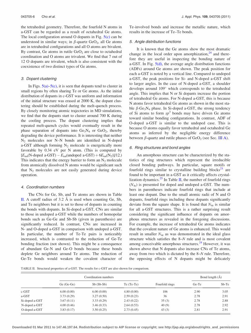
the tetrahedral geometry. Therefore, the fourfold N atoms in
a-GST can be regarded as a result of octahedral Ge atoms.
The local configuration around O dopants in Fig. 5(c) can be
understood in similar ways; in b-quartz GeO2, all Ge atoms
are in tetrahedral configurations and all O atoms are bivalent.
By contrast, Ge atoms in rutile GeO2 are close to octahedral
coordination and O atoms are trivalent. We find that 7 out of
12 O dopants are trivalent, which is also consistent with the
coexistence of two distinct types of Ge atoms.
3. Dopant clustering
In Figs. 5(a)–5(c), it is seen that dopants tend to cluster in
small regions by often sharing Te or Ge atoms. As the initial
distribution of dopants in c-GST was uniform and information
of the initial structure was erased at 2000 K, the dopant clus-
tering should be established during the melt-quench process.
By closely monitoring atomic trajectories in MD simulations,
we find that the dopants start to cluster around 700 K during
the cooling process. The dopant clustering implies that
repeated melt-quench cycles would eventually result in the
phase separation of dopants into Ge3N4 or GeO2, thereby
degrading the device performance. It is interesting that neither
N2 molecules nor N–N bonds are identified in N-doped
a-GST although forming N2 molecule is energetically more
favorable by 0.34 eV per N atom. (This is computed by
[Etot(N-doped a-GST) – Etot(undoped a-GST)þ 6Etot(N2)]/12.)
This indicates that the energy barrier to form an N2 molecule
from atomically dissolved N atoms would be significant such
that N2 molecules are not easily generated during device
operation.
4. Coordination numbers
The CNs for Ge, Sb, and Te atoms are shown in Table
II. A cutoff radius of 3.2 A is used when counting Ge, Sb,
and Te neighbors but it is set to those of dopants in counting
the bonds with dopants. In Si-doped a-GST, CNs are similar
to those in undoped a-GST while the numbers of homopolar
bonds such as Ge-Ge and Sb-Sb (given in parenthesis) are
significantly reduced. In contrast, CNs are increased in
N- and O-doped a-GST in comparison with undoped a-GST.
In particular, the number of Te-Te pairs is noticeably
increased, which is contrasted to the reduction of Ge-Te
bonding fraction (not shown). This might be a consequence
of abundant Ge-N and Ge-O bonds because these bonds
deplete Ge neighbors around Te atoms. The reduction of
Ge-Te bonds would weaken the covalent character of
Te-involved bonds and increase the metallic nature, which
results in the increase of Te–Te bonds.
5. Angle distribution functions
It is known that the Ge atoms show the most dramatic
change in the local order upon amorphization,24 and there-
fore they are useful in inspecting the bonding nature of
a-GST. In Fig. 5(d), the average angle distribution functions
(ADFs) around Ge atoms are shown. The peak position for
each a-GST is noted by a vertical line. Compared to undoped
a-GST, the peak positions for Si- and N-doped a-GST shift
to larger angles. In the case of N-doped a-GST, a shoulder
develops around 109� which corresponds to the tetrahedral
angle. This implies that N or Si dopants increase the portion
of tetrahedral Ge atoms. For N-doped a-GST, this is because
N atoms favor tetrahedral Ge atoms as shown in the most sta-
ble b-Ge3N4 phase. In Si-doped a-GST, the strong tendency
of Si atoms to form sp3 bonds may have driven Ge atoms
toward similar bonding configurations. In contrast, ADF of
O-doped a-GST is similar to the undoped case. This is
because O atoms equally favor tetrahedral and octahedral Ge
atoms as inferred by the negligible energy difference
between b-quartz and rutile phases of GeO2 (see Sec. III A).
6. Ring structures and bond angles
An amorphous structure can be characterized by the sta-
tistics of ring structures which represent the irreducible
closed bonding pathways. In particular, square motifs or
fourfold rings similar to crystalline building blocks21 are
found to be important in a-GST as it critically affects crystal-
lization dynamics.25 In Table II, the number of fourfold rings
(N4r) is presented for doped and undoped a-GST. The num-
bers in parentheses indicate fourfold rings that include at
least one dopant. Due to the small atomic radii of N and O
dopants, fourfold rings including these dopants significantly
deviate from the square shape. It is found that N4r is similar
for all a-GST structures. This is a rather surprising result
considering the significant influence of dopants on amor-
phous structures as revealed in the foregoing discussions.
For example, the increase of tetrahedral Ge atoms indicates
that the covalent nature of Ge atoms is enhanced. This would
result in smaller N4r as was demonstrated in the ideal glass
structure which satisfies the 8–N rule and is most covalent
among conceivable amorphous structures.24 However, it was
shown above that N dopants also increase CNs of Te atoms,
away from two which is dictated by the 8–N rule. Therefore,
the opposing effects of N dopants might be delicately
TABLE II. Structural properties of a-GST. The results for c-GST are also shown for comparison.
Coordination numbers Bond length (A)
Ge (Ge-Ge) Sb (Sb-Sb) Te (Te-Te) Fourfold rings Ge-Te Sb-Te
c-GST 6.00 (0.00) 6.00 (0.00) 4.80 (0.00) 106 2.90 3.05
a-GST 3.73 (0.29) 3.27 (0.50) 2.59 (0.23) 36 2.78 2.91
Si-doped a-GST 3.67 (0.11) 3.33 (0.29) 2.43 (0.22) 35 (3) 2.78 2.88
N-doped a-GST 4.00 (0.46) 3.46 (0.33) 2.64 (0.53) 40 (9) 2.78 2.92
O-doped a-GST 3.83 (0.17) 3.50 (0.25) 2.73 (0.45) 43 (3) 2.81 2.91
043705-6 Cho et al. J. Appl. Phys. 109, 043705 (2011)
Downloaded 01 Mar 2011 to 147.46.197.64. Redistribution subject to AIP license or copyright; see http://jap.aip.org/about/rights_and_permissions
balanced and result in the similar N4r to the undoped case. In
Table II, we also examine average bond lengths in a-GST. It
is found that Ge–Te and Sb–Te bond lengths change by less
than 0.03 A with doping. This is consistent with extended
x-ray absorption fine structure (EXAFS) results in Ref. 12
which showed that N-doping up to 26 at. % did not affect
Ge-Te distances. The small change also supports that the
overall bonding character is not affected much by dopants.
7. Energetic stability
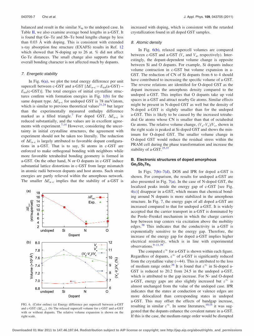
In Fig. 6(a), we plot the total energy difference per unit
supercell between c-GST and a-GST [DEa–c¼Etot(a-GST) –
Etot(c-GST)]. The total energies of initial crystalline struc-
tures confirm with formation energies in Fig. 1(b) for the
same dopant type. DEa–c for undoped GST is 78 meV/atom,
which is similar to previous theoretical values21,24 but larger
than the experimentally measured enthalpy difference
marked as a filled triangle.7 For doped GST, DEa–c is
reduced substantially, and the values are in excellent agree-
ments with experiment.7,14 However, considering the uncer-
tainty in initial crystalline structures, the agreement with
experiment should not be taken too literally. The reduction
of DEa–c is largely attributed to favorable dopant configura-
tions in a-GST. That is to say, Si atoms in c-GST are
enforced to make orthogonal bonding with neighbors while
more favorable tetrahedral bonding geometry is formed in
a-GST. On the other hand, N or O dopants in c-GST induce
substantial lattice distortions in c-GST from large mismatch
in atomic radii between dopants and host atoms. Such strain
energies are partly relieved within the amorphous network.
The smaller DEa–c implies that the stability of a-GST is
increased with doping, which is consistent with the retarded
crystallization found in all doped GST samples.
8. Atomic density
In Fig. 6(b), relaxed supercell volumes are compared
between c-GST and a-GST (Vc and Va, respectively). Inter-
estingly, the dopant-dependent volume change is opposite
between Si and O dopants. For example, Si dopants induce
volume contraction in c-GST but volume expansion in a-
GST. The reduction of CN of Si dopants from 6 to 4 should
have contributed to increasing the specific volume of a-GST.
The reverse relations are identified for O-doped GST as the
dopant increases the amorphous density compared to the
undoped a-GST. This implies that O dopants take up void
spaces in a-GST and attract nearby Ge atoms. Similar effects
might be present in N-doped GST as well but the density of
N-doped a-GST is slightly smaller than for the undoped
a-GST. This is likely to be caused by the increased tetrahe-
dral Ge atoms whose CN is smaller than that of octahedral
Ge atoms. The relative volume change, (Va–Vc)/Vc, shown in
the right scale is peaked at Si-doped GST and shows the min-
imum for O-doped GST. The smaller volume change in
O-doped GST would reduce the residual stress within the
PRAM cell during the phase transformation and increase the
stability of a-GST.25,37
B. Electronic structures of doped amorphousGe2Sb2Te5
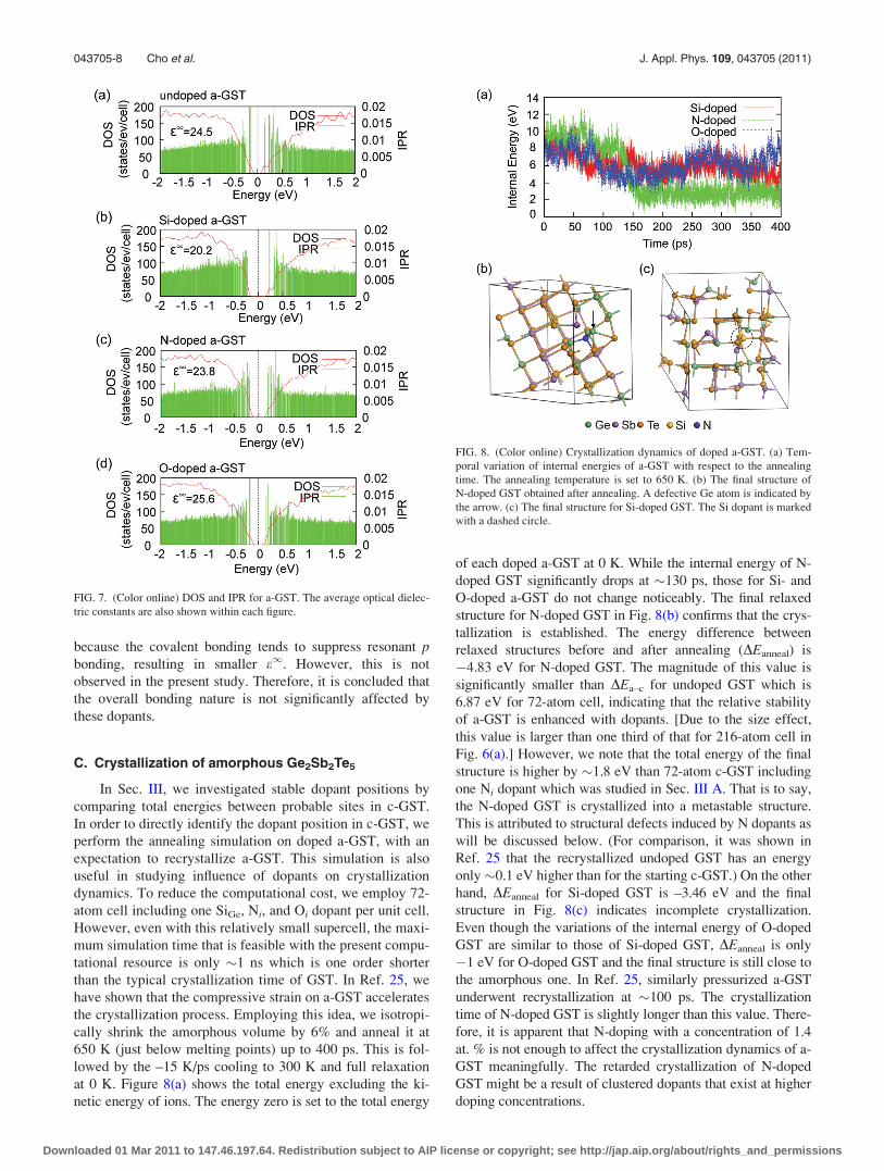
In Figs. 7(b)–7(d), DOS and IPR for doped a-GST is
shown. For comparison, the results for undoped a-GST are
also presented in Fig. 7(a). In the case of N-doped GST, the
localized peaks inside the energy gap of c-GST [see Fig.
4(c)] disappear in a-GST, which means that chemical bond-
ing around N dopants is more stabilized in the amorphous
structure. In Fig. 7, the energy gaps of all doped a-GST are
increased compared to that for undoped a-GST. It is widely
accepted that the carrier transport in a-GST is dominated by
the Poole–Frenkel mechanism in which the charge carriers
hop between trap centers via excitation above the mobility
edges.38 This indicates that the conductivity in a-GST is
exponentially sensitive to the energy gap. Therefore, the
increase of the energy gap for doped a-GST implies higher
electrical resistivity, which is in line with experimental
observations.9–11,39
The computed e1 for a-GST is shown within each figure.
Regardless of dopants, e1 of a-GST is significantly reduced
from the crystalline value (�44). This is attributed to the loss
of medium range order.26 It is found that e1 in Si-doped a-
GST is reduced to 20.2 from 24.5 in the undoped a-GST,
which is attributed to the gap increase. For N- and O-doped
a-GST, energy gaps are also slightly increased but e1 is
almost unchanged from the value of the undoped case. IPR
indicates that the states at conduction or valence edges are
more delocalized than corresponding states in undoped
a-GST. This may offset the effects of bandgap increase,
resulting in similar e1. In some literatures,10,14 it was sug-
gested that the dopants enhance the covalent nature in a-GST.
If this is the case, the medium-range order would be disrupted
FIG. 6. (Color online) (a) Energy difference per supercell between a-GST
and c-GST (DEa–c). (b) The relaxed supercell volume for c-GST and a-GST
with or without dopants. The relative volume expansion is shown on the
right scale.
043705-7 Cho et al. J. Appl. Phys. 109, 043705 (2011)
Downloaded 01 Mar 2011 to 147.46.197.64. Redistribution subject to AIP license or copyright; see http://jap.aip.org/about/rights_and_permissions
because the covalent bonding tends to suppress resonant pbonding, resulting in smaller e1. However, this is not
observed in the present study. Therefore, it is concluded that
the overall bonding nature is not significantly affected by
these dopants.
C. Crystallization of amorphous Ge2Sb2Te5
In Sec. III, we investigated stable dopant positions by
comparing total energies between probable sites in c-GST.
In order to directly identify the dopant position in c-GST, we
perform the annealing simulation on doped a-GST, with an
expectation to recrystallize a-GST. This simulation is also
useful in studying influence of dopants on crystallization
dynamics. To reduce the computational cost, we employ 72-
atom cell including one SiGe, Ni, and Oi dopant per unit cell.
However, even with this relatively small supercell, the maxi-
mum simulation time that is feasible with the present compu-
tational resource is only �1 ns which is one order shorter
than the typical crystallization time of GST. In Ref. 25, we
have shown that the compressive strain on a-GST accelerates
the crystallization process. Employing this idea, we isotropi-
cally shrink the amorphous volume by 6% and anneal it at
650 K (just below melting points) up to 400 ps. This is fol-
lowed by the –15 K/ps cooling to 300 K and full relaxation
at 0 K. Figure 8(a) shows the total energy excluding the ki-
netic energy of ions. The energy zero is set to the total energy
of each doped a-GST at 0 K. While the internal energy of N-
doped GST significantly drops at �130 ps, those for Si- and
O-doped a-GST do not change noticeably. The final relaxed
structure for N-doped GST in Fig. 8(b) confirms that the crys-
tallization is established. The energy difference between
relaxed structures before and after annealing (DEanneal) is
�4.83 eV for N-doped GST. The magnitude of this value is
significantly smaller than DEa–c for undoped GST which is
6.87 eV for 72-atom cell, indicating that the relative stability
of a-GST is enhanced with dopants. [Due to the size effect,
this value is larger than one third of that for 216-atom cell in
Fig. 6(a).] However, we note that the total energy of the final
structure is higher by �1.8 eV than 72-atom c-GST including
one Ni dopant which was studied in Sec. III A. That is to say,
the N-doped GST is crystallized into a metastable structure.
This is attributed to structural defects induced by N dopants as
will be discussed below. (For comparison, it was shown in
Ref. 25 that the recrystallized undoped GST has an energy
only�0.1 eV higher than for the starting c-GST.) On the other
hand, DEanneal for Si-doped GST is –3.46 eV and the final
structure in Fig. 8(c) indicates incomplete crystallization.
Even though the variations of the internal energy of O-doped
GST are similar to those of Si-doped GST, DEanneal is only
�1 eV for O-doped GST and the final structure is still close to
the amorphous one. In Ref. 25, similarly pressurized a-GST
underwent recrystallization at �100 ps. The crystallization
time of N-doped GST is slightly longer than this value. There-
fore, it is apparent that N-doping with a concentration of 1.4
at. % is not enough to affect the crystallization dynamics of a-
GST meaningfully. The retarded crystallization of N-doped
GST might be a result of clustered dopants that exist at higher
doping concentrations.
FIG. 7. (Color online) DOS and IPR for a-GST. The average optical dielec-
tric constants are also shown within each figure.
FIG. 8. (Color online) Crystallization dynamics of doped a-GST. (a) Tem-
poral variation of internal energies of a-GST with respect to the annealing
time. The annealing temperature is set to 650 K. (b) The final structure of
N-doped GST obtained after annealing. A defective Ge atom is indicated by
the arrow. (c) The final structure for Si-doped GST. The Si dopant is marked
with a dashed circle.
043705-8 Cho et al. J. Appl. Phys. 109, 043705 (2011)
Downloaded 01 Mar 2011 to 147.46.197.64. Redistribution subject to AIP license or copyright; see http://jap.aip.org/about/rights_and_permissions
The N dopant in the crystallized GST is bonded with
three Ge atoms and one Sb atom with mean distances of 2.02
and 2.39 A, respectively [see Fig. 8(b)]. Among them, two of
the three Ge atoms were bonded in the initial amorphous
structure and they are not broken during the recrystallization
process. The final structure in Fig. 8(b) is similar to NTe or
Ni studied in the above, which validates the energetic stabil-
ity in Fig. 1(b) computed with crystalline structures. How-
ever, the Ge atom indicated by the arrow in Fig. 8(b) is not
compatible with the rocksalt-style atomic registry and intro-
duces significant lattice deformation around the dopant. To
be specific, the defective Ge atom rotates the crystallo-
graphic orientations of neighboring Te atoms, which can be
regarded as a primitive form of the grain boundary. On the
other hand, neighboring atoms of Si (three Te atoms and one
Sb atom) are different from the neighbors in the starting
amorphous phase and they are bonded during annealing.
This indicates that Si-Te bonds are weaker than Ge-N bonds.
The Si dopant in Fig. 8(c) is still tetrahedrally coordinated
even though most atoms are aligned with the rocksalt struc-
ture. This observation implies that the energy barrier from
tetrahedral sp3 bonding to orthogonal p-bonding network (so
called “umbrella flipping”40) would be significant for Si
atoms, which would constitute a microscopic origin of the
impeded crystallization in Si-doped GST.
V. CONCLUSIONS
In conclusion, we performed extensive ab initio calcula-
tions on the crystalline and amorphous structures of GST
doped with Si, N, and O atoms, aiming to explain pro-
nounced effects of dopants at the atomic level. In the crystal-
line phase, the most favorable doping site for Si was SiGe
while N and O dopants favor interstitial or substitutional Te
sites due to strong Ge–N or Ge–O bonds. However, the com-
parison of lattice parameters with experiment indicates that
interstitial dopants should exist in significant amounts. The
analysis on DOS indicates that the localization at the valence
top increases for N- or O-doped c-GST, which increases re-
sistivity of p-type c-GST. The amorphous structures of
doped GST were obtained by melt-quench simulations. It
was found that each dopant formed preferential bonding
such as Si–Te, Ge–N, and Ge–O pairs. In particular, the local
bonding structures around N or O atoms were well explained
based on crystalline structures of Ge3N4 and GeO2. This is
similar to the crystalline phase but the local bonding geome-
try is more favorable in the amorphous phase, which
accounts for the increased stability of doped a-GST. The
analysis on the local structure did not support the viewpoint
that the bonding character is significantly changed toward
the covalent character. The N dopant enhanced the covalent
character of Ge but this was counterbalanced by the
increased metallic nature of Te atoms. Nevertheless, Si
atoms were found to be most effective in fundamentally
affecting bonding nature of a-GST among the studied dop-
ants. We also carried out annealing simulations on a-GST
and the atomic structure of recrystallized N-doped GST was
close to that for the Ni dopant in c-GST. However, the strong
tendency of the N dopant to form bonds with Ge atoms gave
rise to significant lattice deformations akin to the grain
boundary. The Si-doped GST was partially crystallized but
Si atoms remained in the tetrahedral configuration. The com-
parison of the crystallization time with the undoped case
directly confirmed that Si and O dopants slow down the crys-
tallization process of a-GST. By enlightening the local struc-
tures of representative dopants and relating electronic and
atomic structures to material properties, present theoretical
results will serve as a useful guideline in choosing optimal
dopants to engineer specific properties of GST.
ACKNOWLEDGMENTS
This work was supported by the National Program for
0.1 Terabit NVM Devices and the Fundamental R&D Pro-
gram for Core Technology of Materials funded by the Minis-
try of Knowledge Economy of the Korean Government.
Some parts of the computations were carried out at KISTI
(KSC-2010-C2-0011).
1A. L. Lacaita and D. J. Wouters, Phys. Status Solidi A 205, 2281 (2008).2B. Qiao, J. Feng, Y. Lai, Y. Ling, Y. Lin, T. Tang, B. Cai, and B. Chen,
Appl. Surf. Sci. 252, 8404 (2006).3J. Feng, Y. Zhang, B. W. Qiao, Y. F. Lai, Y. Y. Lin, B. C. Cai, T. A. Tang,
and B. Chen, Appl. Phys. A 87, 57 (2007).4H. Kolpin, D. Music, G. Laptyeva, R. Ghadimi, F. Merget, S. Richter, R.
Mykhaylonka, J. Mayer, and J. M. Schneider, J. Phys.: Condens. Matter
21, 435501 (2009).5S. M. Kim, J. H. Jun, D. J. Choi, S. K. Hong, and Y. J. Park, Jpn. J. Appl.
Phys. 44, L208 (2005).6R. Kojima, S. Okabayashi, T. Kashihara, K. Horai, T. Matsunaga, E. Ohno,
N. Yamada, and T. Ohta, Jpn. J. Appl. Phys., Part 1 37, 2098 (1998).7T. H. Jeong, M. R. Kim, H. Seo, J. W. Park, and C. Yeon, Jpn. J. Appl.
Phys. 39, 2775 (2000).8H. Seo, T.-H. Jeong, J.-W. Park, C. Yeon, S.-J. Kim, and S.-Y. Kim, Jpn.
J. Appl. Phys., Part 1 39, 745 (2000).9H. Horii, J. H. Yi, J. H. Park, Y. H. Ha, I. G. Baek, S. O. Park, Y. N. Hwang,
S. H. Lee, Y. T. Kim, K. H. Lee, U.-I. Chung, and J. T. Moon, in Proceed-ings of the 2003 Symposium on VLSI Technology (IEEE, Piscataway,
2003), 177.10S. Privitera, E. Rimini, and R. Zonca, Appl. Phys. Lett. 85, 3044 (2004).11B. Liu, Z. Song, T. Zhang, J. Xia, S. Feng, and B. Chen, Thin Solid Films
478, 49 (2005).12Y. Kim, M. H. Jang, K. Jeong, M.-H. Cho, K. H. Do, D.-H. Ko, H. C.
Sohn, and M. G. Kim, Appl. Phys. Lett. 92, 061910 (2008).13R. M. Shelby and S. Raoux, J. Appl. Phys. 105, 104902 (2009).14T. H. Jeong, H. Seo, K. L. Lee, S. M. Choi, S. J. Kim, and S. Y. Kim, Jpn.
J. Appl. Phys. 40, 1609 (2001).15S. M. Jeong, K. H. Kim, S. M. Choi, and H. L. Lee, Jpn. J. Appl. Phys. 48,
045503 (2009).16K. B. Borisenko, Y. Chen, S. Song, and D. J. H. Cockayne, Chem. Mater.
21, 5244 (2009).17Z. Sun, J. Zhou, and R. Ahuja, Phys. Rev. Lett. 96, 055507 (2006).18J.-H. Eom, Y.-G. Yoon, C. Park, H. Lee, J. Im, D.-S. Suh, J.-S. Noh, Y.
Khang, and J. Ihm, Phys. Rev. B 73, 214202 (2006).19J. Akola and R. O. Jones, Phys. Rev. B 76, 235201 (2007).20S. Caravati, M. Bernasconi, T. D. Kuhne, M. Krack, and M. Parrinello,
Appl. Phys. Lett. 91, 171906 (2007).21J. Hegedus and S. R. Elliott, Nat. Mater. 7, 399 (2008).22J. Akola, R. O. Jones, S. Kohara, S. Kimura, K. Kobayashi, M. Takata, T.
Matsunaga, R. Kojima, and N. Yamada, Phys. Rev. B 80, 020201(R)
(2009).23Z. Sun, J. Zhou, A. Blomqvist, B. Johansson, and R. Ahuja, Phys. Rev.
Lett. 102, 075504 (2009).24E. Cho, J. Im, C. Park, W. J. Son, D. Kim, H. Horii, J. Ihm, and S. Han, J.
Phys.: Condens. Matter 22, 205504 (2010).25J. Im, E. Cho, D. Kim, H. Horii, J. Ihm, and S. Han, Phys. Rev. B 81,
245211 (2010).26B. Huang and J. Robertson, Phys. Rev. B 81, 081204(R) (2010).
043705-9 Cho et al. J. Appl. Phys. 109, 043705 (2011)
Downloaded 01 Mar 2011 to 147.46.197.64. Redistribution subject to AIP license or copyright; see http://jap.aip.org/about/rights_and_permissions
27Z. Sun, J. Zhou, H. Shin, A. Blomqvist, and R. Ahuja, Appl. Phys. Lett.
93, 241908 (2008).28S. J. Kim, J. H. Choi, S. C. Lee, B. Cheong, D. S. Jeong, and C. Park,
J. Appl. Phys. 107, 103522 (2010).29G. Kresse and J. Hafner, Phys. Rev. B 47, 558 (1993).30P. E. Blochl, Phys. Rev. B 50, 17953 (1994).31J. P. Perdew, K. Burke, and M. Ernzerhof, Phys. Rev. Lett. 77, 3865
(1996).32CRC Handbook of Chemistry and Physics, 66th ed., edited by R. C. Weast
(CRC Press, Boca Raton, 1986).33K. Kim, J.-C. Park, J.-G. Chung, S. A. Song, M.-C. Jung, Y. M. Lee,
H.-J. Shin, B. Kuh, Y. Ha, and J.-S. Noh, Appl. Phys. Lett. 89, 243520
(2006).
34B. S. Lee, J. R. Abelson, S. G. Bishop, D.-H. Kang, B. Cheong, and K.-B.
Kim, J. Appl. Phys. 97, 093509 (2005).35S. Caravati, M. Bernasconi, T. D. Kuhne, M. Krack, and M. Parrinello, J.
Phys.: Condens. Matter 21, 255501 (2009).36J. Dong, O. F. Sankey, S. K. Deb, G. Wolf, and P. F. McMillan, Phys.
Rev. B 61, 11979 (2000).37M. Mitra, Y. Jung, D. S. Gianola, and R. Agarwal, Appl. Phys. Lett. 96,
222111 (2010).38D. Ielmini and Y. Zhang, J. Appl. Phys. 102, 054517 (2007).39Y. Kim, U. Hwang, Y. J. Cho, H. M. Park, M. –H. Cho, P. Cho, and J.
Lee, Appl. Phys. Lett. 90, 021908 (2007).40A. V. Kolobov, P. Fons, A. I. Frenkel, A. L. Ankudinov, J. Tominaga, and
T. Uruga, Nat. Mater. 3, 703 (2004).
043705-10 Cho et al. J. Appl. Phys. 109, 043705 (2011)
Downloaded 01 Mar 2011 to 147.46.197.64. Redistribution subject to AIP license or copyright; see http://jap.aip.org/about/rights_and_permissions