Embed Size (px)
Citation preview
NATURE MATERIALS | VOL 10 | FEBRUARY 2011 | www.nature.com/naturematerials 91
Early on in semiconductor research, the ubiquity of unintentional dopants meant that reproducible results were rare; as late as 1931, physicist Wolfgang Pauli opined in a letter1 to Rudolph Peierls
that “one shouldn’t work on semiconductors, that is a !lthy mess; who knows whether any semiconductors exist.” Eight decades later, the purity of germanium is better than 1 part in 1011, permitting almost nine orders of magnitude variability in doping concentration. Silicon purity is similar. Yet even with this current exquisite control, the dopants usually still play a supporting role in current devices, by mod-ifying the chemical potential of a material. At these levels of purity, each unintentional dopant is on average more than a micrometre away from any other unintentional dopant. "us devices on the nano-scale can be expected to have absolutely no unintentional dopants, and if the doping is carefully controlled a device can be constructed with one and only one dopant — a solitary dopant opto electronic, or solotronic, device. And, as atoms are the building blocks of mat-ter, a solotronic device is where the miniaturization of semiconductor devices reaches the limits set by the discrete nature of matter.
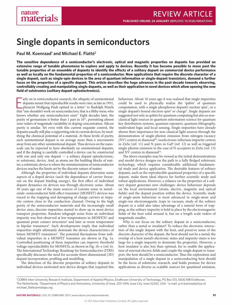
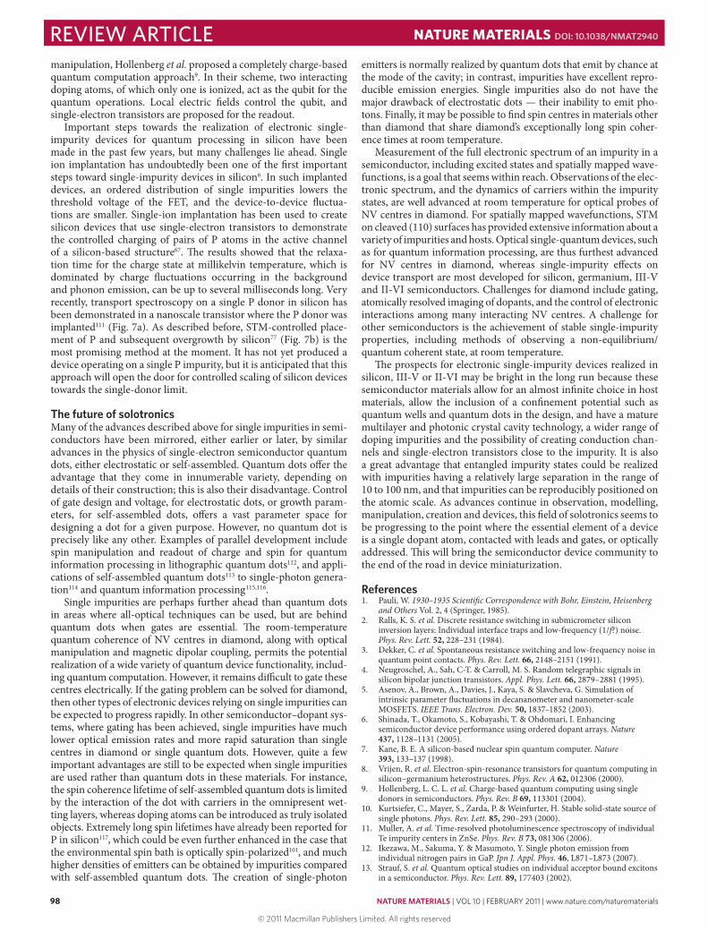
Although the properties of individual dopants determine some aspects of a doped device (such the dependence of carrier freeze-out on the dopant binding energy), the !rst e#ect of individual dopant dynamics on devices was through electronic noise. About 30 years ago one of the main sources of Lorentz noise in metal–oxide–semiconductor !eld-e#ect transistor (MOSFET) devices was traced to the trapping and detrapping of charge carriers at impu-rity centres close to the conduction channel. Owing to the high purity of the semiconductor materials and the increasingly small device sizes, discrete impurities started to show up in most device transport properties. Random telegraph noise from an individual impurity was !rst observed at low temperatures in MOSFETs2 and quantum point contact structures3 and later at room temperature in bipolar transistors4. Such developments imply that individual impurities might ultimately dominate the device characteristics of future MOSFET transistors5. "e potential $uctuations from indi-vidual impurities in a MOSFET transistor are shown in Fig. 1a. Controlled positioning of these impurities can improve threshold voltage reproducibility for MOSFETs, as shown in Fig. 1b–e (ref. 6). "e International Technology Roadmap for Semiconductors (ITRS) speci!cally discusses the need for accurate three-dimensional (3D) dopant incorporation, pro!ling and modelling.
"e detection of the discrete properties of solitary dopants in individual devices motivated new device designs that required this
Single dopants in semiconductorsPaul M. Koenraad1 and Michael E. Flatté2
The sensitive dependence of a semiconductor’s electronic, optical and magnetic properties on dopants has provided an extensive range of tunable phenomena to explore and apply to devices. Recently it has become possible to move past the tunable properties of an ensemble of dopants to identify the e!ects of a solitary dopant on commercial device performance as well as locally on the fundamental properties of a semiconductor. New applications that require the discrete character of a single dopant, such as single-spin devices in the area of quantum information or single-dopant transistors, demand a further focus on the properties of a specific dopant. This article describes the huge advances in the past decade towards observing, controllably creating and manipulating single dopants, as well as their application in novel devices which allow opening the new field of solotronics (solitary dopant optoelectronics).
behaviour. About 10 years ago it was realized that single impurities could be used to physically realize the ‘qubits’ of quantum computation, with a single phosphorus dopant’s nuclear spin7, or a single dopant’s bound electron spin8 or charge9. Single dopants are suggested not only as qubits for quantum computing but also as non-classical light sources in quantum information science for quantum key distribution systems, quantum repeaters, quantum lithography, multivalent logic and local sensing. Single impurities have already shown their importance for non-classical light sources through the demonstration of single-photon emission from nitrogen-vacancy (NV) centres in diamond10, isoelectronic tellurium impurity centres in ZnSe (ref. 11) and N pairs in GaP (ref. 12) as well as triggered single-photon emission in the case of N-acceptors in ZnSe (ref. 13) and NV centres in diamond14.
"e above examples may be viewed as the initial demonstrations and model device designs on the path to a fully $edged solotronic technology, which requires considerable additional fundamen-tal study and device application. "e desirable features of solitary dopants, such as the reproducible quantized properties of a speci!c dopant, make them ideal objects for further scienti!c study and robust applications. However, a reliance on the properties of a soli-tary dopant generates new challenges: device behaviour depends on the local environment (strain, electric, magnetic and optical !elds) and the dopant position within the device. Scienti!c study of single-atom behaviour is most advanced in single-atom and single-ion electromagnetic traps in vacuum; study of the solitary dopant in a solid also takes advantage of a natural form of trap-ping, as the solitary impurity is held in place by the electromagnetic !elds of the host solid around it, but on a length scale orders of magnitude smaller.
Why is our focus on the solitary dopant in a semiconductor, rather than a metal or insulator? To reduce the electronic interac-tion of the single dopant with the host, and preserve some of the discrete character of the dopant, the host should not be a metal; the overlap of a host metal’s electronic states and impurity states is too large for a single impurity to dominate the properties. However, a host insulator is also less than optimal, for to enable the applica-tion of external electric !elds and couple the single dopant to trans-port, the host should be a semiconductor. "us the exploration and manipulation of a single dopant in a semiconducting host should be the focus of solotronic research, and holds promise for device applications as diverse as scalable sources for quantized emission,
1COBRA Inter-University Research Institute, Department of Applied Physics, Eindhoven University of Technology, PO Box 513, 5600 MB Eindhoven, The Netherlands. 2Department of Physics and Astronomy, University of Iowa, 203 VAN, Iowa City, Iowa 52242, USA. *e-mail: [email protected]; [email protected]
REVIEW ARTICLEPUBLISHED ONLINE: 24 JANUARY 2011!|!DOI: 10.1038/NMAT2940
nmat_2940_FEB11.indd 91 11/1/11 11:56:33
© 2011 Macmillan Publishers Limited. All rights reserved
92 NATURE MATERIALS | VOL 10 | FEBRUARY 2011 | www.nature.com/naturematerials
qubits for quantum computation and elements in multivalent logic. Recent scienti!c developments have brought these options within reach, through experimental advances in scanning probe microscopy, confocal microscopy and single-impurity implanta-tion. "ese new techniques are able to address, manipulate and even arrange individual impurities. We thus have reached a point where one can start to unravel the interaction of a single impurity with its environment, pioneer the construction of single-impurity devices and explore fundamental quantum-mechanical processes on indi-vidually addressable impurities.
Observing single impurities"e !rst electronic observation of a single impurity in a semiconduc-tor material was made in a MOSFET device cooled to low tempera-ture2. A single bistable impurity close to the conduction channel was responsible for the observed random telegraph noise. "e observa-tion of random telegraph noise due to single impurities in nanos-tructured devices is now rather common3, but it remains a challenge
to obtain detailed information about the responsible impurity itself. One exception is the use of noise in a conduction channel to measure the spin state of a single impurity8. A spin-to-charge transformation can occur when the impurity, by virtue of the Pauli principle, can only bind a second electron with opposite spin. Recently this tactic was applied to monitor the spin resonance of a single paramagnetic impurity at the Si/SiO2 interface15.
Single impurities also manifested their presence in tunnel-ling. In a double-barrier resonant-tunnelling (DBRT) diode with a micrometre-sized diameter, features in the I–V curves could be related to the presence of a single Si donor in the DBRT well16. Although DBRT structures enabled the determination of the spin-splitting of an individual Si doping atom located in a GaAs quantum well17 as well as located in an AlAs barrier18, and an estimate of the extension of the wavefunction of the impurity state19, their use is o%en hampered by the uncontrolled incorporation and unknown chemical nature of the impurity state. Other tunnelling approaches have used a single impurity to scan the density-of-states (DOS) spectrum of a two-dimensional electron gas20 or shown the presence of a single impurity in industrial-type nano-MOSFETs21,22.
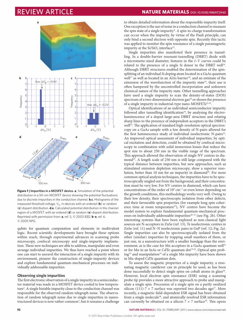
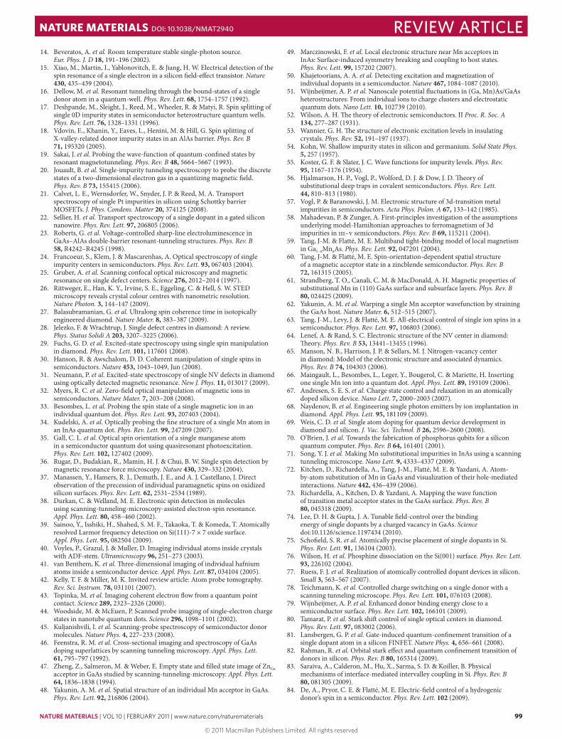
Optical identi!cations of an individual semiconductor impurity followed a%er tunnelling identi!cation16, by analysing the electro-luminescence of a doped large-area DBRT structure and relating sharp lines to the presence of independent acceptors in the DBRT’s well23. "e application of standard high-resolution optical spectros-copy on a GaAs sample with a low density of N-pairs allowed for the !rst luminescence study of individual isoelectronic N-pairs24. An improved optical assessment of individual impurities, by opti-cal excitation and detection, could be obtained by confocal micro-scopy in combination with solid immersion lenses that reduce the spot size to about 250 nm in the visible range of the spectrum. "is approach allowed the observation of single NV centres in dia-mond25. A length scale of 250 nm is still large compared with the typical distance between impurities, but new approaches, such as stimulated emission depletion microscopy, show a superior reso-lution, better than 10 nm for an impurity in diamond26. For more common optical analysis techniques, the impurities have to be spec-troscopically singled out from the background, and their concentra-tion must be very low. For NV centres in diamond, which can have concentrations of the order of 109 cm&3 or even lower depending on the growth conditions, this methodology works very well. Owing to their low density, their spectroscopic isolation from other defects, and their favourable spin properties (for example long spin coher-ence time at room temperature27), NV centres have become the model system to explore fundamental quantum-mechanical proc-esses on individually addressable impurities28–31 (see Fig. 2b). Other interesting systems that have been explored as non-classical light sources are N-acceptors in ZnSe (ref. 13), Te isoelectronic centres in ZnSe (ref. 11) and N–N isoelectronic pairs in GaP (ref. 12; Fig. 2a). Single impurities can also be spectroscopically isolated from the other (similar) impurities by trapping small numbers of them, or just one, in a nanostructure with a smaller bandgap than the envi-ronment, as is the case for Mn acceptors in a GaAs quantum well32 or for Mn in an InAs or CdTe quantum dot33,34. Optical spin prob-ing33 and manipulation35 of a single Mn impurity have been shown in Mn-doped CdTe quantum dots.
To assess the magnetic properties of a single impurity, a reso-nating magnetic cantilever can in principle be used, as has been done successfully to detect single spins on cobalt atoms in glass36. However, local electron spin resonance (ESR) using a scanning probe tip provides a more attractive approach to probe and manip-ulate a single spin. Precession of a single spin on a partly oxidized silicon (111)-7 ' 7 surface was reported two decades ago37. More recently, a magnetic-!eld-dependent ESR signal has been obtained from a single molecule38, and atomically resolved ESR information can currently be obtained on a silicon 7 ' 7 surface39. "is opens
a
b c
Freq
uency
8
7
6
5
4
3
2
1
0
Freq
uency
8
7
6
5
4
3
2
1
0
1.2m
Source
Drain
100 nm
d
–2 –1 1 20Vth [V]
–2 –1 1 20Vth [V]
Ave. Vth = –0.4V
Ave. Vth = –0.2V
e
Source
Drain
300 nm
Figure 1 | Impurities in a MOSFET device. a, Simulation of the potential distribution in a 50-nm MOSFET device showing the potential fluctuations due to discrete impurities in the conduction channel. b,c, Histograms of the measured threshold voltage, Vth, in devices with an ordered (b) or random (c) dopant distribution. d,e, Calculated potential distribution in the channel region of a MOSFET with an ordered (d) or random (e) dopant distribution. Reprinted with permission from: a, ref. 5, © 2003 IEEE; b–e, ref. 6, © 2005 NPG.
REVIEW ARTICLE NATURE MATERIALS DOI: 10.1038/NMAT2940
nmat_2940_FEB11.indd 92 11/1/11 11:56:36
© 2011 Macmillan Publishers Limited. All rights reserved
NATURE MATERIALS | VOL 10 | FEBRUARY 2011 | www.nature.com/naturematerials 93
the route to applying the scanning probe ESR technique to single impurities. "e spin information it provides might solve one of the most important outstanding problems for conventional scanning tunnelling microscopy: how to determine the chemical nature of the impurity under the scanning tip.
Observing the spatial location of single impurities in a semi-conductor material has been a longstanding challenge for trans-mission electron microscopy. "is was only recently resolved a%er the development of annular dark-!eld scanning transmission elec-tron microscopy with a spatial resolution of about 0.2 nm. "e !rst observations of single impurities by this technique were made40 on Sb atoms in Si. "e same technique in combination with series of through-focus images was !nally able to pinpoint the 3D position of individual Hf atoms near a MOSFET interface with an accuracy of 0.5 nm (ref. 41; Fig. 2c). A serious limitation of this technique is the weak scattering of electrons by some impurity species, rendering them undetectable. Promising results in the !eld of 3D tomo graphy of impurities in semiconductors include the observation of the 3D distribution of (impurity) atoms with a so-called atom probe. "is technique removes atoms layer-by-layer by !eld emission, and uses spatially resolved time-of-$ight analysis to determine the origi-nal location and atomic mass of the detected atoms42. "e di(cult reconstruction process needed to determine the original position of the detected atoms and impurities in the material and the fact that only a fraction of all atoms can be detected remain serious chal-lenges for this new technique.
In the !eld of scanning probe microscopy, the positions of impurity atoms were revealed by their impact on the electron propagation as visualized by a scanning gate probe tip43. Later, this scanning gate technique was able to resolve directly the position of individual impurities in a carbon nanotube44. Scanning probe capacitance spectroscopy was able to resolve the 2D distribution of silicon atoms in a delta-doped plane in GaAs with a spatial resolu-tion of a few nanometres45.
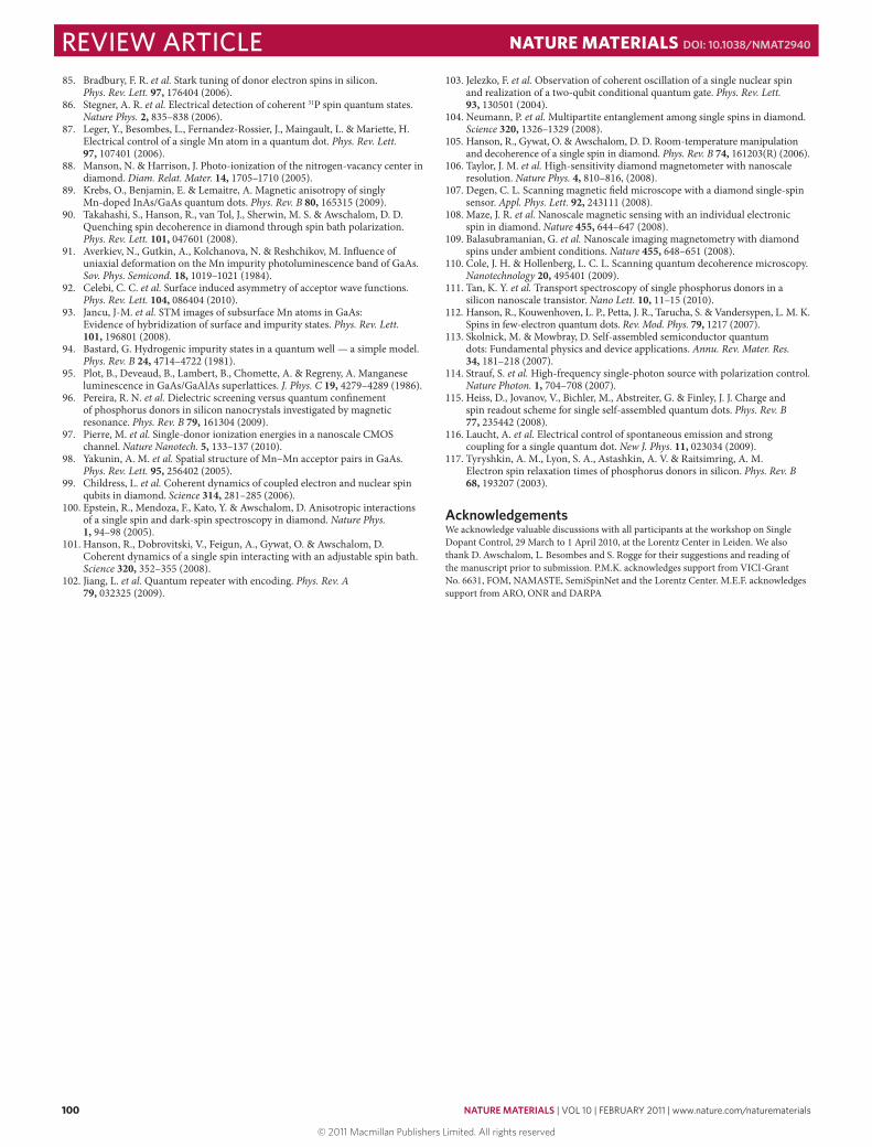
Scanning tunnelling microscopy (STM) performed on the cleaved edge of a semiconductor crystal remains the most powerful tech-nique to observe single impurities. Even in some of the !rst meas-urements using this technique, individual Si donors in GaAs (ref. 46) and Zn acceptors in GaAs (ref. 47) were clearly recognized. "e local tip-induced band bending allowed the observation of these impuri-ties in their neutral as well as their charged state. Cross-sectional scanning tunnelling microscopy (XSTM) analysis of Mn acceptors in their neutral state made it possible to analyse and understand the anisotropic charge distribution of the hole bound to the Mn accep-tor48 (see Fig. 2d). By now, spectroscopic details and the atomically precise 3D position of individual impurities can be determined49. Unfortunately the XSTM technique is mainly limited to the natural (110) cleavage plane of III-V and II-VI semi conductor materials.
In conclusion, the most advanced techniques at the moment for observing single impurities are optical spectroscopy (especially for NV centres in diamond), transport spectroscopy in silicon nano-MOSFETS, and XSTM for impurities in III-V and II-VI materials. "e STM technique shows great promise because of its atomic reso-lution, wavefunction imaging and charge manipulation possibilities and the prospects for a combined electric, magnetic and optical analysis. Obtaining magnetic information, such as spin detection, on a single impurity remains a considerable challenge for STM, but recently the !rst successful analysis of a magnetic Fe impurity in the surface layer of InSb has been reported50. Additional interesting approaches in this respect are local ESR and STM-induced lumines-cence. Examples of observational challenges are related to the detec-tion and manipulating of single mobile and interstitial impurities51.
Modelling of impurity states"e marked e#ect of impurities on the properties of semiconduc-tors motivated intense theoretical investigation into their properties early in the history of the !eld. Almost immediately, the essential character of impurity states was proposed, as localized states within a bandgap52. An expansion of the wavefunction in single-particle localized (Wannier) states, producing a recognizable e#ective-mass equation for shallow, Coulombic, bound states, was performed barely a decade53 a%er the derivation of the Schrödinger equation. "is approach was subsequently placed on a solid formal footing even when many-body e#ects were considered54. Strong, short-range potentials, which generate deep levels within the gap, can be e(ciently treated using Green’s function techniques to determine the structure near the impurity55.
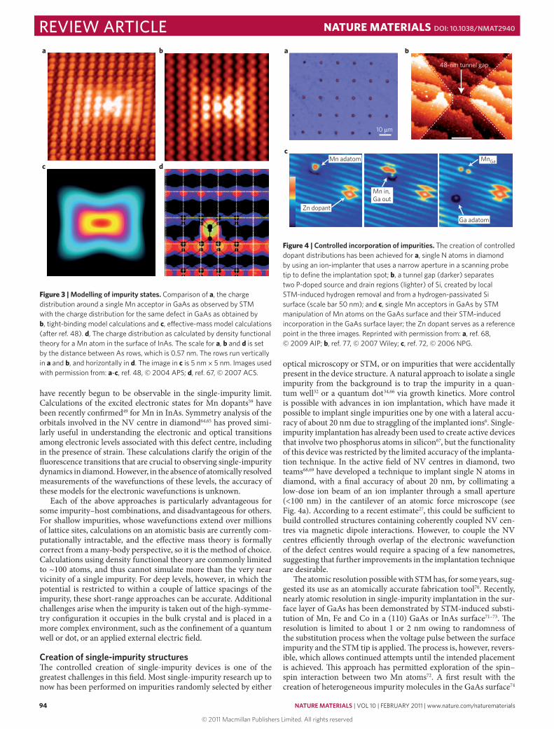
In III-V zincblende semiconductors these potentials originate from an on-site potential from the impurity atom and hybridiza-tion between the tetrahedrally coordinated dangling bonds of the surrounding host and the orbitals of the impurity atom56. For tran-sition-metal substitutional dopants in III-V zincblende semicon-ductors, the partially !lled d orbitals of the impurity atom will split into a tightly bound set of orbitals corresponding to the E irreduc-ible representation of the tetrahedral point group, which have poor overlap with dangling bonds of the nearest-neighbour host atoms, and an extended set of orbitals of p-like symmetry (corresponding to the T2 irreducible representation), which overlap well with the host57. "is symmetry-based analysis of the orbitals, introduced in a tight-binding basis56,57, applies equally well to calculations of such deep levels performed with density functional theory58. "e symme-try of the bonding in the crystal dominates the wavefunction sym-metry of these substitutional dopants48,59 (Fig. 3), with a smaller, but identi!able, e#ect of spin–orbit interactions60,61. Symmetry analysis also provides the low-energy Hamiltonian for strain62 and electric !elds63 acting on the impurity state, but quantitative values for the resulting electronic energies require a calculation based on one of the above methods.
Internal transitions among the electronic states of the impurity can be detected in a variety of ways in macroscopic ensembles, but
NV1
NV2
[001]
[110]
41
6
3 7
95
82
P
2 ma
c d
b
f+/–0.0 nm
Figure 2 | Imaging of single impurities. Examples of individual impurities in a semiconductor material as observed by several techniques. Observation of a, N–N pairs in GaP’. b, NV centres in diamond by scanning confocal microscopy; c, a single Hf atom at the Si–SiO interface by scanning transmission electron microscopy; and d, Mn acceptors in GaAs by cross-section STM. The numbers indicate the depth in atomic layers of the Mn layer below the (110) cleavage surface, and p indicates a Mn atom coupled to an adsorbate. Reprinted with permission from: a, ref. 12, © 2007 JSAP; b, ref. 29, © 2008 APS; c, ref. 41, © 2005 AIP; d, ref. 92, © 2010 APS.
REVIEW ARTICLENATURE MATERIALS DOI: 10.1038/NMAT2940
nmat_2940_FEB11.indd 93 11/1/11 11:56:38
© 2011 Macmillan Publishers Limited. All rights reserved
94 NATURE MATERIALS | VOL 10 | FEBRUARY 2011 | www.nature.com/naturematerials
have recently begun to be observable in the single-impurity limit. Calculations of the excited electronic states for Mn dopants59 have been recently con!rmed49 for Mn in InAs. Symmetry analysis of the orbitals involved in the NV centre in diamond64,65 has proved simi-larly useful in understanding the electronic and optical transitions among electronic levels associated with this defect centre, including in the presence of strain. "ese calculations clarify the origin of the $uorescence transitions that are crucial to observing single-impurity dynamics in diamond. However, in the absence of atomically resolved measurements of the wavefunctions of these levels, the accuracy of these models for the electronic wavefunctions is unknown.
Each of the above approaches is particularly advantageous for some impurity–host combinations, and disadvantageous for others. For shallow impurities, whose wavefunctions extend over millions of lattice sites, calculations on an atomistic basis are currently com-putationally intractable, and the e#ective mass theory is formally correct from a many-body perspective, so it is the method of choice. Calculations using density functional theory are commonly limited to ~100 atoms, and thus cannot simulate more than the very near vicinity of a single impurity. For deep levels, however, in which the potential is restricted to within a couple of lattice spacings of the impurity, these short-range approaches can be accurate. Additional challenges arise when the impurity is taken out of the high-symme-try con!guration it occupies in the bulk crystal and is placed in a more complex environment, such as the con!nement of a quantum well or dot, or an applied external electric !eld.
Creation of single-impurity structures"e controlled creation of single-impurity devices is one of the greatest challenges in this !eld. Most single-impurity research up to now has been performed on impurities randomly selected by either
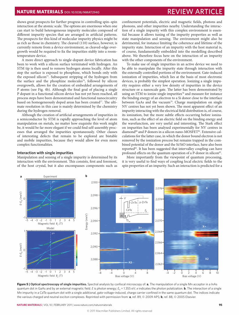
optical microscopy or STM, or on impurities that were accidentally present in the device structure. A natural approach to isolate a single impurity from the background is to trap the impurity in a quan-tum well32 or a quantum dot34,66 via growth kinetics. More control is possible with advances in ion implantation, which have made it possible to implant single impurities one by one with a lateral accu-racy of about 20 nm due to straggling of the implanted ions6. Single-impurity implantation has already been used to create active devices that involve two phosphorus atoms in silicon67, but the functionality of this device was restricted by the limited accuracy of the implanta-tion technique. In the active !eld of NV centres in diamond, two teams68,69 have developed a technique to implant single N atoms in diamond, with a !nal accuracy of about 20 nm, by collimating a low-dose ion beam of an ion implanter through a small aperture (<100 nm) in the cantilever of an atomic force microscope (see Fig. 4a). According to a recent estimate27, this could be su(cient to build controlled structures containing coherently coupled NV cen-tres via magnetic dipole interactions. However, to couple the NV centres e(ciently through overlap of the electronic wavefunction of the defect centres would require a spacing of a few nanometres, suggesting that further improvements in the implantation technique are desirable.
"e atomic resolution possible with STM has, for some years, sug-gested its use as an atomically accurate fabrication tool70. Recently, nearly atomic resolution in single-impurity implantation in the sur-face layer of GaAs has been demonstrated by STM-induced substi-tution of Mn, Fe and Co in a (110) GaAs or InAs surface71–73. "e resolution is limited to about 1 or 2 nm owing to randomness of the substitution process when the voltage pulse between the surface impurity and the STM tip is applied. "e process is, however, revers-ible, which allows continued attempts until the intended placement is achieved. "is approach has permitted exploration of the spin–spin interaction between two Mn atoms72. A !rst result with the creation of heterogeneous impurity molecules in the GaAs surface74
a
c d
b
Figure 3 | Modelling of impurity states. Comparison of a, the charge distribution around a single Mn acceptor in GaAs as observed by STM with the charge distribution for the same defect in GaAs as obtained by b, tight-binding model calculations and c, e!ective-mass model calculations (after ref. 48). d, The charge distribution as calculated by density functional theory for a Mn atom in the surface of InAs. The scale for a, b and d is set by the distance between As rows, which is 0.57 nm. The rows run vertically in a and b, and horizontally in d. The image in c is 5 nm ' 5 nm. Images used with permission from: a-c, ref. 48, © 2004 APS; d, ref. 67, © 2007 ACS.
Mn adatom
Zn dopant
MnGa
Mn in,Ga out
Ga adatom
a b
c
10 m
48-nm tunnel gap
Figure 4 | Controlled incorporation of impurities. The creation of controlled dopant distributions has been achieved for a, single N atoms in diamond by using an ion-implanter that uses a narrow aperture in a scanning probe tip to define the implantation spot; b, a tunnel gap (darker) separates two P-doped source and drain regions (lighter) of Si, created by local STM-induced hydrogen removal and from a hydrogen-passivated Si surface (scale bar 50 nm); and c, single Mn acceptors in GaAs by STM manipulation of Mn atoms on the GaAs surface and their STM-induced incorporation in the GaAs surface layer; the Zn dopant serves as a reference point in the three images. Reprinted with permission from: a, ref. 68, © 2009 AIP; b, ref. 77, © 2007 Wiley; c, ref. 72, © 2006 NPG.
REVIEW ARTICLE NATURE MATERIALS DOI: 10.1038/NMAT2940
nmat_2940_FEB11.indd 94 11/1/11 11:56:42
© 2011 Macmillan Publishers Limited. All rights reserved
NATURE MATERIALS | VOL 10 | FEBRUARY 2011 | www.nature.com/naturematerials 95
shows great prospects for further progress in controlling spin–spin interaction at the atomic scale. "e options are enormous when one can start to build heterogeneous impurity molecules composed of di#erent impurity species that are arranged in arti!cial patterns. "e prospects for this kind of molecular impurity physics might be as rich as those in chemistry. "e cleaved (110) surface, however, is currently remote from a device environment, as cleaved-edge over-growth would be required to !x the impurities stably into a room-temperature device.
A more direct approach to single-dopant device fabrication has been to work with a silicon surface terminated with hydrogen. An STM tip is then used to remove hydrogen atoms locally. A%er this step the surface is exposed to phosphine, which bonds only with the exposed silicon75. Subsequent stripping of the hydrogen from the surface and the phosphine molecules76, followed by silicon overgrowth, allows for the creation of embedded arrangements of P atoms (see Fig. 4b). Although the !nal goal of placing a single P dopant in a functional silicon device has not yet been reached, all process steps have been demonstrated and functional nanocircuitry based on homogeneously doped areas has been created77. "e ulti-mate resolution in this case is mainly determined by the chemistry during the hydrogen removal.
Although the creation of arti!cial arrangements of impurities in a semiconductor by STM is rapidly approaching the level of atom manipulation on metals, no matter how exquisite this work might be, it would be far more elegant if we could !nd self-assembly proc-esses that arranged the impurities spontaneously. Other classes of interesting defects that remain to be explored are bistable and mobile impurities, because they would allow for even more complex functionalities.
Interaction with single impuritiesManipulation and sensing of a single impurity is determined by its interaction with the environment. "is consists, !rst and foremost, of the host crystal, but it also encompasses components such as
con!nement potentials, electric and magnetic !elds, photons and phonons, and other impurities nearby. Understanding the interac-tion of a single impurity with this complex environment is essen-tial because it allows tuning of the impurity properties as well as state manipulation and sensing. "e environment might also be detrimental, for instance limiting the coherence and lifetime of the impurity state. Interaction of an impurity with the host material is, of course, fundamentally embedded into the modelling described above. We therefore focus here on the interaction of an impurity with the other components of the environment.
To make use of single impurities in an active device we need to be able to manipulate the impurity state through interaction with the externally controlled portions of the environment. Gate-induced ionization of impurities, which lies at the basis of most electronic devices, is probably the simplest operation. Ionizing a single impu-rity requires either a very low density of impurities in the device structure or a nanoscale gate. "e latter has been demonstrated by using an STM to ionize single impurities78 and measure for instance the binding energy of an electron to a Si donor close to the interface between GaAs and the vacuum79. Charge manipulation on single NV centres has not yet been shown. "e most apparent e#ect of an impurity interacting with the electrical !eld distribution is, of course, its ionization, but the more subtle e#ects occurring before ioniza-tion, such as the e#ect of an electric !eld on the binding energy and the wavefunction, are very useful and interesting. "e Stark e#ect on impurities has been analysed experimentally for NV centres in diamond80 and P donors in a silicon nano-MOSFET81. Extensive cal-culations for the latter case, in which the donor bound electron is not removed by the ionization process but remains trapped in the com-bined potential of the donor and the Si/SiO interface, have also been reported82. It has been suggested that intervalley coupling can have profound e#ects on the quantum operation of a P-donor in silicon83.
More importantly from the viewpoint of quantum processing, it is very useful to !nd ways of coupling local electric !elds to the spin properties of an impurity. Such an interaction is predicted for a
–1
1
0
–1
1
0
–5 –4 –3 –2 –1 1 2 3 4 50
Experiment
Model
–a b
Magnetic field Bz (T)
Magnetic field Bz (T)–5 –4 –3 –2 –1 1 2 3 4 50
E–E 0
(meV
)E–E 0
(meV
)
+
+
Al
Vi-ZnTe p-ZnTe
CdTe EF
Dss
X
X+
X–
X2
X
X+
X–
X2
2,100
2,098
2,096
2,094
2,092
Ener
gy (m
eV)
2,090
2,088
2,062
2,064
2,066
2,068
2,070
2,072
2,074
2,076
–8 –4 –4 –2 2 4 6 8 104 80 0Bias voltage (V) Bias voltage (V)
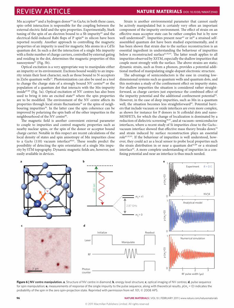
Figure 5 | Optical spectroscopy of single impurities. Spectral analysis by confocal microscopy of: a, The manipulation of a single Mn acceptor in a InAs quantum dot in GaAs and by an external magnetic field. E is photon energy; E0 = 1.355 eV; ! indicates the photon polatization. b, The interaction of a single Mn impurity in a CdTe quantum dot with a single additional, gate-voltage-induced, charge carrier confined in the same quantum dot. The indices indicate the various charged and neutral exciton complexes. Reprinted with permission from: a, ref. 89, © 2009 APS; b, ref. 88, © 2005 Elsevier.
REVIEW ARTICLENATURE MATERIALS DOI: 10.1038/NMAT2940
nmat_2940_FEB11.indd 95 11/1/11 11:56:48
© 2011 Macmillan Publishers Limited. All rights reserved
96 NATURE MATERIALS | VOL 10 | FEBRUARY 2011 | www.nature.com/naturematerials
Mn acceptor63 and a hydrogen donor84 in GaAs; in both these cases, spin–orbit interaction is responsible for the coupling between the external electric !eld and the spin properties. Experimentally, Stark tuning of the spin of an electron bound to a Sb impurity85 and the electrical-!eld-induced Rabi $ops of P spin86 in silicon have been reported recently. Another approach to controlling the magnetic properties of an impurity is used for magnetic Mn atoms in a CdTe quantum dot. In such a dot the interaction of a single Mn impurity with a !nite number of charge carriers, controlled by external gating and residing in the dot, determines the magnetic properties of this nanosystem87 (Fig. 5b).
Optical excitation is a very appropriate way to manipulate either an impurity or its environment. Excitons bound weakly to an impu-rity retain their host character, such as those bound to N-acceptors in ZnSe quantum wells13. Photoionization can also be used as a tool to change the charge state of a strongly bound NV centre88 or the population of a quantum dot that interacts with the Mn-impurity inside87,89 (Fig. 5a). Optical excitation of NV centres has also been used to bring it into an excited state29 where the spin properties are to be modi!ed. "e environment of the NV centre a#ects its properties through local strain $uctuations29 or the spins of neigh-bouring impurities30. In the latter case the spin coherence can be improved by polarizing the spin bath of the other impurities in the neighbourhood of the NV centre90.
"e magnetic !eld is another convenient external parameter to couple to impurities and control magnetic properties such as nearby nuclear spins, or the spin of the donor or acceptor bound charge carrier. Notable in this respect are recent calculations of the local density of states and spin anisotropy of Mn impurities close to a GaAs (110) vacuum interface60,61. "ese results predict the possibility of detecting the spin orientation of a single Mn impu-rity by STM topography. Dynamic magnetic !elds are, however, not easily available in devices.
Strain is another environmental parameter that cannot easily be actively manipulated but is certainly very o%en an important component of the impurity environment. "e e#ect of strain on an e#ective mass acceptor state can be rather complex but is by now well understood91. Impurities present near62 or in89 a strained self-assembled quantum dot have been studied experimentally, and it has been shown that strain due to the surface reconstruction is an essential ingredient in understanding the behaviour of impurities below a reconstructed surface61,92,93. "e latter result applies to all impurities observed by XSTM, especially the shallow impurities that couple most strongly with the surface. "e above strains are static; dynamic strain, such as from a phonon, provides a potential addi-tional method of manipulating single-dopant electronic structure.
"e advantage of semiconductors is the ease in creating low-dimensional systems such as quantum wells and quantum dots, and this motivates a study of the con!nement e#ect on impurity states. For shallow impurities the situation is considered rather straight-forward, as charge carriers just experience the combined e#ect of the impurity potential and the additional con!nement potential94. However, in the case of deep impurities, such as Mn in a quantum well, the situation becomes less straightforward95. Potential barri-ers that include vacuum or oxide interfaces are even more complex, as shown for instance for P donors in Si colloidal dots and nano-MOSFETS, for which the change of localization is dominated by a reduction of dielectric screening96,97, and at vacuum–semiconductor interfaces, where a recent study of Si impurities close to the GaAs–vacuum interface showed that e#ective mass theory breaks down79 and strain induced by surface reconstruction plays an essential role61,92,93. If the behaviour of impurities is well understood, how-ever, they could act as a local sensor to probe local properties such the strain distribution in or near a quantum dot62,89 or a strained interface92. A more complete understanding of impurities in a con-!ning potential and near an interface is thus much needed.
2 µm
c
V
N
b ea
d
Laser
RF
Photoncounter
Initialize
Manipulate
Readout
532
nm
2.87 GHz
ms= ±1
ms= 0
Experiment
0
1
0
1Analytical model
00 1 2 3
1Numerical simulation
RF pulse width (µs)
B = 0 G
NV14
Experiment B = 0 G
NV14
p (m
s=0)
p (m
s=0)
p (m
s=0)
Figure 6 | NV centre manipulation. a, Structure of NV centre in diamond; b, energy level structure; c, optical imaging of NV centres; d, pulse sequence for spin manipulation; e, measurements of response of the single impurity to the pulse sequence, along with theoretical results. p(ms = 0) indicates the probability of the spin in the zero spin-projection state. Reprinted with permission from ref. 101, © 2008 APS.
REVIEW ARTICLE NATURE MATERIALS DOI: 10.1038/NMAT2940
nmat_2940_FEB11.indd 96 11/1/11 11:56:50
© 2011 Macmillan Publishers Limited. All rights reserved
NATURE MATERIALS | VOL 10 | FEBRUARY 2011 | www.nature.com/naturematerials 97
"e study of impurity–impurity interaction is still an open !eld, and thus far only some !rst results for isolated Mn–Mn pairs have been published72,98 and some !rst results on the spin lifetime of small clusters of Mn acceptors in a GaAs quantum well32. Studying such impurity–impurity interaction is not only essential for the compre-hension of impurity band formation, which is an important issue in magnetic semiconductors such as GaMnAs, but likely to be reward-ing for the understanding and use of entangled impurity states, and will also allow us to understand how to read out the spin state of one impurity by probing another coupled impurity.
Single-impurity devicesTo meet the ultimate challenge in single-impurity physics, the creation of functional single-impurity devices for quantum informa-tion processing, several proposals have been presented and investi-gated. "ese concepts and their (partial) realizations can broadly be split into optical and electronic devices. NV centres in diamond and other optically active defects in semiconductors fall into the category of optical devices, whereas those based on spin prepara-tion, manipulation and detection by local gates and single-electron transistors fall into the category of electronic devices.
A !rst step towards the application of single impurities and defects in optical devices involves the triggered emission of single photons. "is has been demonstrated successfully for N-acceptors in ZnSe quantum wells13 and NV centres in diamond14. "is is a !rst step towards using single impurities as a single-photon source for quantum key distribution in quantum secure communication. Optical probing33 and orientation35 of a single Mn spin has been shown for an isolated Mn atom in a CdTe quantum dot. Spectacular progress has been seen in the past few years in quantum informa-tion processing on NV. "is has been shown by a successful prepa-ration of the spin state of a NV centre by means of optical excitation, manipulation by RF !elds and optical readout28,99–102 (see Fig. 6). Although the NV centre is a point defect and its electron spin is mostly localized at the defect site, some of its electron spin den-sity is distributed over the nearest-neighbour carbon atoms. As a
result, substantial hyper!ne and dipolar coupling are present owing to single nuclei localized close to the defect. "e coupling has been used to control the nuclear spin on a single C nucleus to realize a two-qubit conditional quantum gate103. By controlling the nuclear spin on two individual C nuclei in a nearest-neighbour position, the entanglement of their spins was shown104. In another approach it has been shown that one can probe isolated N spins using an NV centre105. Building on such successes in this rapidly expanding !eld, new device concepts based on NV centres, for instance a quantum repeater102, are currently proposed. Interestingly, a single NV centre has also been used as a probe to sense non-invasively the magnetic !eld distribution at the nanoscale106–109, and recently the idea has been put forward to use a single NV centre in a scanning quantum decoherence microscope110 (Fig. 7c).
A number of electronic device concepts have been suggested for the quantum manipulation of a single impurity. Kane proposed that information could be encoded onto the nuclear spins of P atoms in silicon electronic devices7. Logical quantum operations on the individual nuclear spins could then be performed by using externally applied electric !elds that control the electronic bound state around the P atom, which couples both to other P atoms and to the nuclear spin. "e nuclear spins would then be read out by a charge-based method using spin-polarized electrons that directly probed the electronic bound state around the P atoms. Vrijen et al. proposed a SiGe transistor that exploits band-structure engineering to sense and control a single-donor electron spin8. It is proposed that by applying a gate bias, one- and two-qubit operations could be performed, because the electrical !eld could be used to pull the elec-tron wavefunction away from the dopant ion into layers of di#er-ent composition having a di#erent g-factor. Owing to the variation of the g-factor, this displacement changes the spin Zeeman energy, allowing qubit operations. Readout of the spin information would be performed indirectly by a charge-based approach using a current $owing close to the impurity, which owing to the Pauli exclusion principle can only bind a second electron when this has opposite spin to the !rst. Whereas both previous schemes are based on spin
P implantsite
Control site(no implants)
P implantsite Barrier
gate
BarriergateTop
gate
Barriergate
(VBG)
(VTG)
200 nmS
D
a
b
c
Qubit probe
x
y
Weak decoherence
Measurementsignal
Combined temporal/spatial image map
Field map(static)
Hxy xy
Fluctuation map(dynamic)
Correlatedsignal
Spectralresponse
Strong decoherence
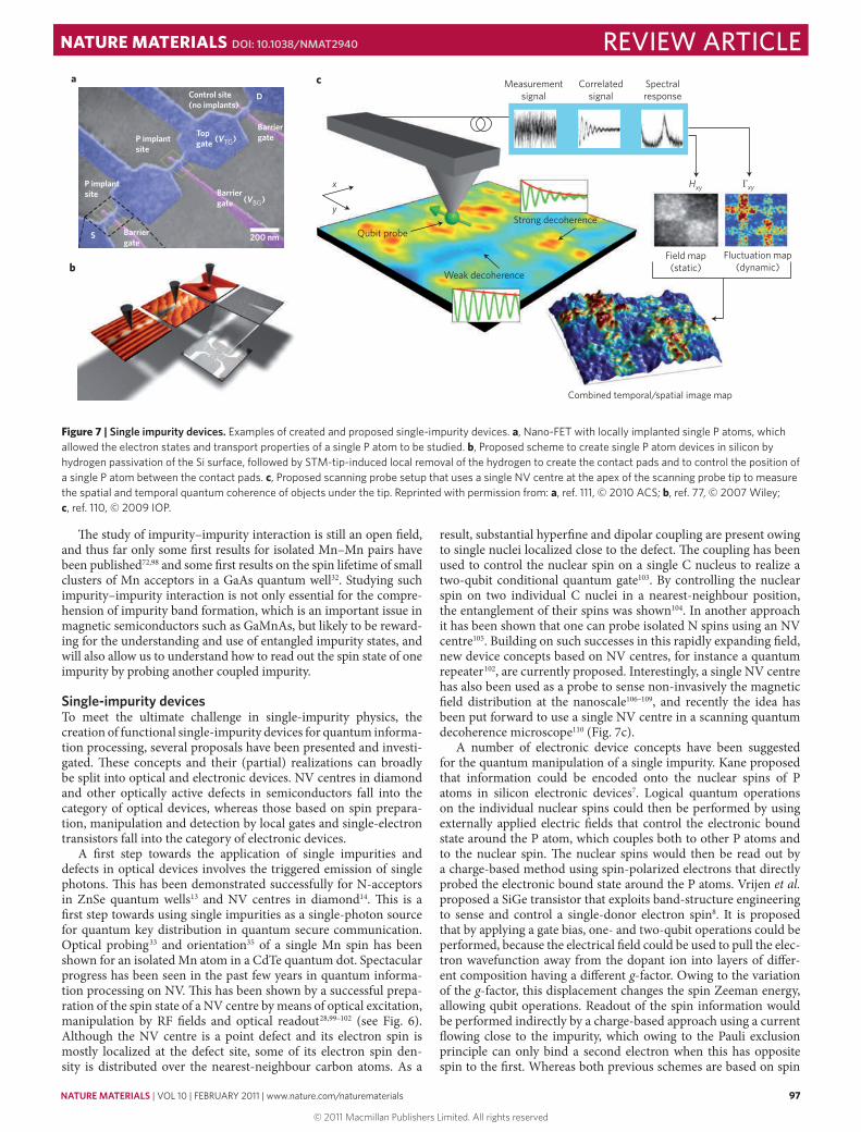
Figure 7 | Single impurity devices. Examples of created and proposed single-impurity devices. a, Nano-FET with locally implanted single P atoms, which allowed the electron states and transport properties of a single P atom to be studied. b, Proposed scheme to create single P atom devices in silicon by hydrogen passivation of the Si surface, followed by STM-tip-induced local removal of the hydrogen to create the contact pads and to control the position of a single P atom between the contact pads. c, Proposed scanning probe setup that uses a single NV centre at the apex of the scanning probe tip to measure the spatial and temporal quantum coherence of objects under the tip. Reprinted with permission from: a, ref. 111, © 2010 ACS; b, ref. 77, © 2007 Wiley; c, ref. 110, © 2009 IOP.
REVIEW ARTICLENATURE MATERIALS DOI: 10.1038/NMAT2940
nmat_2940_FEB11.indd 97 11/1/11 11:57:07
© 2011 Macmillan Publishers Limited. All rights reserved
98 NATURE MATERIALS | VOL 10 | FEBRUARY 2011 | www.nature.com/naturematerials
manipulation, Hollenberg et al. proposed a completely charge-based quantum computation approach9. In their scheme, two interacting doping atoms, of which only one is ionized, act as the qubit for the quantum operations. Local electric !elds control the qubit, and single-electron transistors are proposed for the readout.
Important steps towards the realization of electronic single-impurity devices for quantum processing in silicon have been made in the past few years, but many challenges lie ahead. Single ion implantation has undoubtedly been one of the !rst important steps toward single-impurity devices in silicon6. In such implanted devices, an ordered distribution of single impurities lowers the threshold voltage of the FET, and the device-to-device $uctua-tions are smaller. Single-ion implantation has been used to create silicon devices that use single-electron transistors to demonstrate the controlled charging of pairs of P atoms in the active channel of a silicon-based structure67. "e results showed that the relaxa-tion time for the charge state at millikelvin temperature, which is dominated by charge $uctuations occurring in the background and phonon emission, can be up to several milliseconds long. Very recently, transport spectroscopy on a single P donor in silicon has been demonstrated in a nanoscale transistor where the P donor was implanted111 (Fig. 7a). As described before, STM-controlled place-ment of P and subsequent overgrowth by silicon77 (Fig. 7b) is the most promising method at the moment. It has not yet produced a device operating on a single P impurity, but it is anticipated that this approach will open the door for controlled scaling of silicon devices towards the single-donor limit.
The future of solotronicsMany of the advances described above for single impurities in semi-conductors have been mirrored, either earlier or later, by similar advances in the physics of single-electron semiconductor quantum dots, either electrostatic or self-assembled. Quantum dots o#er the advantage that they come in innumerable variety, depending on details of their construction; this is also their disadvantage. Control of gate design and voltage, for electrostatic dots, or growth param-eters, for self-assembled dots, o#ers a vast parameter space for designing a dot for a given purpose. However, no quantum dot is precisely like any other. Examples of parallel development include spin manipulation and readout of charge and spin for quantum information processing in lithographic quantum dots112, and appli-cations of self-assembled quantum dots113 to single-photon genera-tion114 and quantum information processing115,116.
Single impurities are perhaps further ahead than quantum dots in areas where all-optical techniques can be used, but are behind quantum dots when gates are essential. "e room-temperature quantum coherence of NV centres in diamond, along with optical manipulation and magnetic dipolar coupling, permits the potential realization of a wide variety of quantum device functionality, includ-ing quantum computation. However, it remains di(cult to gate these centres electrically. If the gating problem can be solved for diamond, then other types of electronic devices relying on single impurities can be expected to progress rapidly. In other semiconductor–dopant sys-tems, where gating has been achieved, single impurities have much lower optical emission rates and more rapid saturation than single centres in diamond or single quantum dots. However, quite a few important advantages are still to be expected when single impurities are used rather than quantum dots in these materials. For instance, the spin coherence lifetime of self-assembled quantum dots is limited by the interaction of the dot with carriers in the omni present wet-ting layers, whereas doping atoms can be introduced as truly isolated objects. Extremely long spin lifetimes have already been reported for P in silicon117, which could be even further enhanced in the case that the environmental spin bath is optically spin-polarized101, and much higher densities of emitters can be obtained by impurities compared with self-assembled quantum dots. "e creation of single-photon
emitters is normally realized by quantum dots that emit by chance at the mode of the cavity; in contrast, impurities have excellent repro-ducible emission energies. Single impurities also do not have the major drawback of electrostatic dots — their inability to emit pho-tons. Finally, it may be possible to !nd spin centres in materials other than diamond that share diamond’s exceptionally long spin coher-ence times at room temperature.
Measurement of the full electronic spectrum of an impurity in a semiconductor, including excited states and spatially mapped wave-functions, is a goal that seems within reach. Observations of the elec-tronic spectrum, and the dynamics of carriers within the impurity states, are well advanced at room temperature for optical probes of NV centres in diamond. For spatially mapped wavefunctions, STM on cleaved (110) surfaces has provided extensive information about a variety of impurities and hosts. Optical single-quantum devices, such as for quantum information processing, are thus furthest advanced for NV centres in diamond, whereas single-impurity e#ects on device transport are most developed for silicon, germanium, III-V and II-VI semiconductors. Challenges for diamond include gating, atomically resolved imaging of dopants, and the control of electronic interactions among many interacting NV centres. A challenge for other semiconductors is the achievement of stable single-impurity properties, including methods of observing a non-equilibrium/quantum coherent state, at room temperature.
"e prospects for electronic single-impurity devices realized in silicon, III-V or II-VI may be bright in the long run because these semiconductor materials allow for an almost in!nite choice in host materials, allow the inclusion of a con!nement potential such as quantum wells and quantum dots in the design, and have a mature multilayer and photonic crystal cavity technology, a wider range of doping impurities and the possibility of creating conduction chan-nels and single-electron transistors close to the impurity. It is also a great advantage that entangled impurity states could be realized with impurities having a relatively large separation in the range of 10 to 100 nm, and that impurities can be reproducibly positioned on the atomic scale. As advances continue in observation, modelling, manipulation, creation and devices, this !eld of solotronics seems to be progressing to the point where the essential element of a device is a single dopant atom, contacted with leads and gates, or optically addressed. "is will bring the semiconductor device community to the end of the road in device miniaturization.
References1. Pauli, W. 1930–1935 Scienti"c Correspondence with Bohr, Einstein, Heisenberg
and Others Vol. 2, 4 (Springer, 1985).2. Ralls, K. S. et al. Discrete resistance switching in submicrometer silicon
inversion layers: Individual interface traps and low-frequency (1/f?) noise. Phys. Rev. Lett. 52, 228–231 (1984).
3. Dekker, C. et al. Spontaneous resistance switching and low-frequency noise in quantum point contacts. Phys. Rev. Lett. 66, 2148–2151 (1991).
4. Neugroschel, A., Sah, C-T. & Carroll, M. S. Random telegraphic signals in silicon bipolar junction transistors. Appl. Phys. Lett. 66, 2879–2881 (1995).
5. Asenov, A., Brown, A., Davies, J., Kaya, S. & Slavcheva, G. Simulation of intrinsic parameter $uctuations in decananometer and nanometer-scale MOSFETS. IEEE Trans. Electron. Dev. 50, 1837–1852 (2003).
6. Shinada, T., Okamoto, S., Kobayashi, T. & Ohdomari, I. Enhancing semiconductor device performance using ordered dopant arrays. Nature 437, 1128–1131 (2005).
7. Kane, B. E. A silicon-based nuclear spin quantum computer. Nature 393, 133–137 (1998).
8. Vrijen, R. et al. Electron-spin-resonance transistors for quantum computing in silicon–germanium heterostructures. Phys. Rev. A 62, 012306 (2000).
9. Hollenberg, L. C. L. et al. Charge-based quantum computing using single donors in semiconductors. Phys. Rev. B 69, 113301 (2004).
10. Kurtsiefer, C., Mayer, S., Zarda, P. & Weinfurter, H. Stable solid-state source of single photons. Phys. Rev. Lett. 85, 290–293 (2000).
11. Muller, A. et al. Time-resolved photoluminescence spectroscopy of individual Te impurity centers in ZnSe. Phys. Rev. B 73, 081306 (2006).
12. Ikezawa, M., Sakuma, Y. & Masumoto, Y. Single photon emission from individual nitrogen pairs in GaP. Jpn J. Appl. Phys. 46, L871–L873 (2007).
13. Strauf, S. et al. Quantum optical studies on individual acceptor bound excitons in a semiconductor. Phys. Rev. Lett. 89, 177403 (2002).
REVIEW ARTICLE NATURE MATERIALS DOI: 10.1038/NMAT2940
nmat_2940_FEB11.indd 98 11/1/11 11:57:07
© 2011 Macmillan Publishers Limited. All rights reserved
NATURE MATERIALS | VOL 10 | FEBRUARY 2011 | www.nature.com/naturematerials 99
14. Beveratos, A. et al. Room temperature stable single-photon source. Eur. Phys. J. D 18, 191–196 (2002).
15. Xiao, M., Martin, I., Yablonovitch, E. & Jiang, H. W. Electrical detection of the spin resonance of a single electron in a silicon !eld-e#ect transistor. Nature 430, 435–439 (2004).
16. Dellow, M. et al. Resonant tunneling through the bound-states of a single donor atom in a quantum-well. Phys. Rev. Lett. 68, 1754–1757 (1992).
17. Deshpande, M., Sleight, J., Reed, M., Wheeler, R. & Matyi, R. Spin splitting of single 0D impurity states in semiconductor heterostructure quantum wells. Phys. Rev. Lett. 76, 1328–1331 (1996).
18. Vdovin, E., Khanin, Y., Eaves, L., Henini, M. & Hill, G. Spin splitting of X-valley-related donor impurity states in an AlAs barrier. Phys. Rev. B 71, 195320 (2005).
19. Sakai, J. et al. Probing the wave-function of quantum-con!ned states by resonant magnetotunneling. Phys. Rev. B 48, 5664–5667 (1993).
20. Jouault, B. et al. Single-impurity tunneling spectroscopy to probe the discrete states of a two-dimensional electron gas in a quantizing magnetic !eld. Phys. Rev. B 73, 155415 (2006).
21. Calvet, L. E., Wernsdorfer, W., Snyder, J. P. & Reed, M. A. Transport spectroscopy of single Pt impurities in silicon using Schottky barrier MOSFETs. J. Phys. Condens. Matter 20, 374125 (2008).
22. Sellier, H. et al. Transport spectroscopy of a single dopant in a gated silicon nanowire. Phys. Rev. Lett. 97, 206805 (2006).
23. Roberts, G. et al. Voltage-controlled sharp-line electroluminescence in GaAs–AlAs double-barrier resonant-tunneling structures. Phys. Rev. B 58, R4242–R4245 (1998).
24. Francoeur, S., Klem, J. & Mascarenhas, A. Optical spectroscopy of single impurity centers in semiconductors. Phys. Rev. Lett. 93, 067403 (2004).
25. Gruber, A. et al. Scanning confocal optical microscopy and magnetic resonance on single defect centers. Science 276, 2012–2014 (1997).
26. Rittweger, E., Han, K. Y., Irvine, S. E., Eggeling, C. & Hell, S. W. STED microscopy reveals crystal colour centres with nanometric resolution. Nature Photon. 3, 144–147 (2009).
27. Balasubramanian, G. et al. Ultralong spin coherence time in isotopically engineered diamond. Nature Mater. 8, 383–387 (2009).
28. Jelezko, F. & Wrachtrup, J. Single defect centres in diamond: A review. Phys. Status Solidi A 203, 3207–3225 (2006).
29. Fuchs, G. D. et al. Excited-state spectroscopy using single spin manipulation in diamond. Phys. Rev. Lett. 101, 117601 (2008).
30. Hanson, R. & Awschalom, D. D. Coherent manipulation of single spins in semiconductors. Nature 453, 1043–1049, Jun (2008).
31. Neumann, P. et al. Excited-state spectroscopy of single NV defects in diamond using optically detected magnetic resonance. New J. Phys. 11, 013017 (2009).
32. Myers, R. C. et al. Zero-!eld optical manipulation of magnetic ions in semiconductors. Nature Mater. 7, 203–208 (2008).
33. Besombes, L. et al. Probing the spin state of a single magnetic ion in an individual quantum dot. Phys. Rev. Lett. 93, 207403 (2004).
34. Kudelski, A. et al. Optically probing the !ne structure of a single Mn atom in an InAs quantum dot. Phys. Rev. Lett. 99, 247209 (2007).
35. Gall, C. L. et al. Optical spin orientation of a single manganese atom in a semiconductor quantum dot using quasiresonant photoexcitation. Phys. Rev. Lett. 102, 127402 (2009).
36. Rugar, D., Budakian, R., Mamin, H. J. & Chui, B. W. Single spin detection by magnetic resonance force microscopy. Nature 430, 329–332 (2004).
37. Manassen, Y., Hamers, R. J., Demuth, J. E., and A. J. Castellano, J. Direct observation of the precession of individual paramagnetic spins on oxidized silicon surfaces. Phys. Rev. Lett. 62, 2531–2534 (1989).
38. Durkan, C. & Welland, M. E. Electronic spin detection in molecules using scanning-tunneling-microscopy-assisted electron-spin resonance. Appl. Phys. Lett. 80, 458–460 (2002).
39. Sainoo, Y., Isshiki, H., Shahed, S. M. F., Takaoka, T. & Komeda, T. Atomically resolved Larmor frequency detection on Si(111)-7 ' 7 oxide surface. Appl. Phys. Lett. 95, 082504 (2009).
40. Voyles, P., Grazul, J. & Muller, D. Imaging individual atoms inside crystals with ADF-stem. Ultramicroscopy 96, 251–273 (2003).
41. van Benthem, K. et al. "ree-dimensional imaging of individual hafnium atoms inside a semiconductor device. Appl. Phys. Lett. 87, 034104 (2005).
42. Kelly, T. F. & Miller, M. K. Invited review article: Atom probe tomography. Rev. Sci. Instrum. 78, 031101 (2007).
43. Topinka, M. et al. Imaging coherent electron $ow from a quantum point contact. Science 289, 2323–2326 (2000).
44. Woodside, M. & McEuen, P. Scanned probe imaging of single-electron charge states in nanotube quantum dots. Science 296, 1098–1101 (2002).
45. Kuljanishvili, I. et al. Scanning-probe spectroscopy of semiconductor donor molecules. Nature Phys. 4, 227–233 (2008).
46. Feenstra, R. M. et al. Cross-sectional imaging and spectroscopy of GaAs doping superlattices by scanning tunneling microscopy. Appl. Phys. Lett. 61, 795–797 (1992).
47. Zheng, Z., Salmeron, M. & Weber, E. Empty state and !lled state image of ZnGa acceptor in GaAs studied by scanning-tunneling-microscopy. Appl. Phys. Lett. 64, 1836–1838 (1994).
48. Yakunin, A. M. et al. Spatial structure of an individual Mn acceptor in GaAs. Phys. Rev. Lett. 92, 216806 (2004).
49. Marczinowski, F. et al. Local electronic structure near Mn acceptors in InAs: Surface-induced symmetry breaking and coupling to host states. Phys. Rev. Lett. 99, 157202 (2007).
50. Khajetoorians, A. A. et al. Detecting excitation and magnetization of individual dopants in a semiconductor. Nature 467, 1084–1087 (2010).
51. Wijnheijmer, A. P. et al. Nanoscale potential $uctuations in (Ga, Mn)As/GaAs heterostructures: From individual ions to charge clusters and electrostatic quantum dots. Nano Lett. 10, 102739 (2010).
52. Wilson, A. H. "e theory of electronic semiconductors. II Proc. R. Soc. A 134, 277–287 (1931).
53. Wannier, G. H. "e structure of electronic excitation levels in insulating crystals. Phys. Rev. 52, 191–197 (1937).
54. Kohn, W. Shallow impurity states in silicon and germanium. Solid State Phys. 5, 257 (1957).
55. Koster, G. F. & Slater, J. C. Wave functions for impurity levels. Phys. Rev. 95, 1167–1176 (1954).
56. Hjalmarson, H. P., Vogl, P., Wolford, D. J. & Dow, J. D. "eory of substitutional deep traps in covalent semiconductors. Phys. Rev. Lett. 44, 810–813 (1980).
57. Vogl, P. & Baranowski, J. M. Electronic structure of 3d-transition metal impurities in semiconductors. Acta Phys. Polon. A 67, 133–142 (1985).
58. Mahadevan, P. & Zunger, A. First-principles investigation of the assumptions underlying model-Hamiltonian approaches to ferromagnetism of 3d impurities in )))–* semiconductors. Phys. Rev. B 69, 115211 (2004).
59. Tang, J-M. & Flatté, M. E. Multiband tight-binding model of local magnetism in Ga1&xMnxAs. Phys. Rev. Lett. 92, 047201 (2004).
60. Tang, J-M. & Flatté, M. E. Spin-orientation-dependent spatial structure of a magnetic acceptor state in a zincblende semiconductor. Phys. Rev. B 72, 161315 (2005).
61. Strandberg, T. O., Canali, C. M. & MacDonald, A. H. Magnetic properties of substitutional Mn in (110) GaAs surface and subsurface layers. Phys. Rev. B 80, 024425 (2009).
62. Yakunin, A. M. et al. Warping a single Mn acceptor wavefunction by straining the GaAs host. Nature Mater. 6, 512–515 (2007).
63. Tang, J-M., Levy, J. & Flatté, M. E. All-electrical control of single ion spins in a semiconductor. Phys. Rev. Lett. 97, 106803 (2006).
64. Lenef, A. & Rand, S. C. Electronic structure of the NV center in diamond: "eory. Phys. Rev. B 53, 13441–13455 (1996).
65. Manson, N. B., Harrison, J. P. & Sellars, M. J. Nitrogen-vacancy center in diamond: Model of the electronic structure and associated dynamics. Phys. Rev. B 74, 104303 (2006).
66. Maingault, L., Besombes, L., Leger, Y., Bougerol, C. & Mariette, H. Inserting one single Mn ion into a quantum dot. Appl. Phys. Lett. 89, 193109 (2006).
67. Andresen, S. E. S. et al. Charge state control and relaxation in an atomically doped silicon device. Nano Lett. 7, 2000–2003 (2007).
68. Naydenov, B. et al. Engineering single photon emitters by ion implantation in diamond. Appl. Phys. Lett. 95, 181109 (2009).
69. Weis, C. D. et al. Single atom doping for quantum device development in diamond and silicon. J. Vac. Sci. Technol. B 26, 2596–2600 (2008).
70. O’Brien, J. et al. Towards the fabrication of phosphorus qubits for a silicon quantum computer. Phys. Rev. B 64, 161401 (2001).
71. Song, Y. J. et al. Making Mn substitutional impurities in InAs using a scanning tunneling microscope. Nano Lett. 9, 4333–4337 (2009).
72. Kitchen, D., Richardella, A., Tang, J-M., Flatté, M. E. & Yazdani, A. Atom-by-atom substitution of Mn in GaAs and visualization of their hole-mediated interactions. Nature 442, 436–439 (2006).
73. Richardella, A., Kitchen, D. & Yazdani, A. Mapping the wave function of transition metal acceptor states in the GaAs surface. Phys. Rev. B 80, 045318 (2009).
74. Lee, D. H. & Gupta, J. A. Tunable !eld-control over the binding energy of single dopants by a charged vacancy in GaAs. Science doi:10.1126/science.1197434 (2010).
75. Scho!eld, S. R. et al. Atomically precise placement of single dopants in Si. Phys. Rev. Lett. 91, 136104 (2003).
76. Wilson, H. et al. Phosphine dissociation on the Si(001) surface. Phys. Rev. Lett. 93, 226102 (2004).
77. Ruess, F. J. et al. Realization of atomically controlled dopant devices in silicon. Small 3, 563–567 (2007).
78. Teichmann, K. et al. Controlled charge switching on a single donor with a scanning tunneling microscope. Phys. Rev. Lett. 101, 076103 (2008).
79. Wijnheijmer, A. P. et al. Enhanced donor binding energy close to a semiconductor surface. Phys. Rev. Lett. 102, 166101 (2009).
80. Tamarat, P. et al. Stark shi% control of single optical centers in diamond. Phys. Rev. Lett. 97, 083002 (2006).
81. Lansbergen, G. P. et al. Gate-induced quantum-con!nement transition of a single dopant atom in a silicon FINFET. Nature Phys. 4, 656–661 (2008).
82. Rahman, R. et al. Orbital stark e#ect and quantum con!nement transition of donors in silicon. Phys. Rev. B 80, 165314 (2009).
83. Saraiva, A., Calderon, M., Hu, X., Sarma, S. D. & Koiller, B. Physical mechanisms of interface-mediated intervalley coupling in Si. Phys. Rev. B 80, 081305 (2009).
84. De, A., Pryor, C. E. & Flatté, M. E. Electric-!eld control of a hydrogenic donor’s spin in a semiconductor. Phys. Rev. Lett. 102 (2009).
REVIEW ARTICLENATURE MATERIALS DOI: 10.1038/NMAT2940
nmat_2940_FEB11.indd 99 11/1/11 11:57:07
© 2011 Macmillan Publishers Limited. All rights reserved
100 NATURE MATERIALS | VOL 10 | FEBRUARY 2011 | www.nature.com/naturematerials
85. Bradbury, F. R. et al. Stark tuning of donor electron spins in silicon. Phys. Rev. Lett. 97, 176404 (2006).
86. Stegner, A. R. et al. Electrical detection of coherent 31P spin quantum states. Nature Phys. 2, 835–838 (2006).
87. Leger, Y., Besombes, L., Fernandez-Rossier, J., Maingault, L. & Mariette, H. Electrical control of a single Mn atom in a quantum dot. Phys. Rev. Lett. 97, 107401 (2006).
88. Manson, N. & Harrison, J. Photo-ionization of the nitrogen-vacancy center in diamond. Diam. Relat. Mater. 14, 1705–1710 (2005).
89. Krebs, O., Benjamin, E. & Lemaitre, A. Magnetic anisotropy of singly Mn-doped InAs/GaAs quantum dots. Phys. Rev. B 80, 165315 (2009).
90. Takahashi, S., Hanson, R., van Tol, J., Sherwin, M. S. & Awschalom, D. D. Quenching spin decoherence in diamond through spin bath polarization. Phys. Rev. Lett. 101, 047601 (2008).
91. Averkiev, N., Gutkin, A., Kolchanova, N. & Reshchikov, M. In$uence of uniaxial deformation on the Mn impurity photoluminescence band of GaAs. Sov. Phys. Semicond. 18, 1019–1021 (1984).
92. Celebi, C. C. et al. Surface induced asymmetry of acceptor wave functions. Phys. Rev. Lett. 104, 086404 (2010).
93. Jancu, J-M. et al. STM images of subsurface Mn atoms in GaAs: Evidence of hybridization of surface and impurity states. Phys. Rev. Lett. 101, 196801 (2008).
94. Bastard, G. Hydrogenic impurity states in a quantum well — a simple model. Phys. Rev. B 24, 4714–4722 (1981).
95. Plot, B., Deveaud, B., Lambert, B., Chomette, A. & Regreny, A. Manganese luminescence in GaAs/GaAlAs superlattices. J. Phys. C 19, 4279–4289 (1986).
96. Pereira, R. N. et al. Dielectric screening versus quantum con!nement of phosphorus donors in silicon nanocrystals investigated by magnetic resonance. Phys. Rev. B 79, 161304 (2009).
97. Pierre, M. et al. Single-donor ionization energies in a nanoscale CMOS channel. Nature Nanotech. 5, 133–137 (2010).
98. Yakunin, A. M. et al. Spatial structure of Mn–Mn acceptor pairs in GaAs. Phys. Rev. Lett. 95, 256402 (2005).
99. Childress, L. et al. Coherent dynamics of coupled electron and nuclear spin qubits in diamond. Science 314, 281–285 (2006).
100. Epstein, R., Mendoza, F., Kato, Y. & Awschalom, D. Anisotropic interactions of a single spin and dark-spin spectroscopy in diamond. Nature Phys. 1, 94–98 (2005).
101. Hanson, R., Dobrovitski, V., Feigun, A., Gywat, O. & Awschalom, D. Coherent dynamics of a single spin interacting with an adjustable spin bath. Science 320, 352–355 (2008).
102. Jiang, L. et al. Quantum repeater with encoding. Phys. Rev. A 79, 032325 (2009).
103. Jelezko, F. et al. Observation of coherent oscillation of a single nuclear spin and realization of a two-qubit conditional quantum gate. Phys. Rev. Lett. 93, 130501 (2004).
104. Neumann, P. et al. Multipartite entanglement among single spins in diamond. Science 320, 1326–1329 (2008).
105. Hanson, R., Gywat, O. & Awschalom, D. D. Room-temperature manipulation and decoherence of a single spin in diamond. Phys. Rev. B 74, 161203(R) (2006).
106. Taylor, J. M. et al. High-sensitivity diamond magnetometer with nanoscale resolution. Nature Phys. 4, 810–816, (2008).
107. Degen, C. L. Scanning magnetic !eld microscope with a diamond single-spin sensor. Appl. Phys. Lett. 92, 243111 (2008).
108. Maze, J. R. et al. Nanoscale magnetic sensing with an individual electronic spin in diamond. Nature 455, 644–647 (2008).
109. Balasubramanian, G. et al. Nanoscale imaging magnetometry with diamond spins under ambient conditions. Nature 455, 648–651 (2008).
110. Cole, J. H. & Hollenberg, L. C. L. Scanning quantum decoherence microscopy. Nanotechnology 20, 495401 (2009).
111. Tan, K. Y. et al. Transport spectroscopy of single phosphorus donors in a silicon nanoscale transistor. Nano Lett. 10, 11–15 (2010).
112. Hanson, R., Kouwenhoven, L. P., Petta, J. R., Tarucha, S. & Vandersypen, L. M. K. Spins in few-electron quantum dots. Rev. Mod. Phys. 79, 1217 (2007).
113. Skolnick, M. & Mowbray, D. Self-assembled semiconductor quantum dots: Fundamental physics and device applications. Annu. Rev. Mater. Res. 34, 181–218 (2007).
114. Strauf, S. et al. High-frequency single-photon source with polarization control. Nature Photon. 1, 704–708 (2007).
115. Heiss, D., Jovanov, V., Bichler, M., Abstreiter, G. & Finley, J. J. Charge and spin readout scheme for single self-assembled quantum dots. Phys. Rev. B 77, 235442 (2008).
116. Laucht, A. et al. Electrical control of spontaneous emission and strong coupling for a single quantum dot. New J. Phys. 11, 023034 (2009).
117. Tyryshkin, A. M., Lyon, S. A., Astashkin, A. V. & Raitsimring, A. M. Electron spin relaxation times of phosphorus donors in silicon. Phys. Rev. B 68, 193207 (2003).
AcknowledgementsWe acknowledge valuable discussions with all participants at the workshop on Single Dopant Control, 29 March to 1 April 2010, at the Lorentz Center in Leiden. We also thank D. Awschalom, L. Besombes and S. Rogge for their suggestions and reading of the manuscript prior to submission. P.M.K. acknowledges support from VICI-Grant No. 6631, FOM, NAMASTE, SemiSpinNet and the Lorentz Center. M.E.F. acknowledges support from ARO, ONR and DARPA
REVIEW ARTICLE NATURE MATERIALS DOI: 10.1038/NMAT2940
nmat_2940_FEB11.indd 100 11/1/11 11:57:07
© 2011 Macmillan Publishers Limited. All rights reserved