Embed Size (px)
Citation preview
1© Springer International Publishing Switzerland 2015 F.L. Deepak et al. (eds.), Advanced Transmission Electron Microscopy, DOI 10.1007/978-3-319-15177-9_1
Chapter 1Aberration-Corrected Electron Microscopy of Nanoparticles
Miguel José Yacamán, Ulises Santiago, and Sergio Mejía-Rosales
1.1 Introduction to Electron Microscopy
1.1.1 Beginnings
The very rich history of electron microscopy started with the discovery of the dual-ity wave–particle. In the 1920s, the beginning of the twentieth century, it was shown that electrons could also behave as a wave. The optical microscopy based on Abbe’s theory already achieved the resolution limit ~ / ~ ,λ 2 2 500Å. The electrons are located at high voltages and hence will have much shorter wavelengths ~0.05 Å. Therefore, since occasionally Abbe’s theory also holds for electromagnetic lenses, a sub-Å resolution could be achieved, and atomic resolution will be possible. The job to build an electron microscope was passed from the physicists to the electric engineers. Shortly after obtaining his doctoral degree, Ernst Ruska took the job. As Ruska describes in his Nobel lecture,
After having shown in my Studienarbeit of 1929 that sharp and magnified images of electron- irradiated hole apertures could be obtained with the short coil, I was now inter-ested in finding out if such images—as in light optics—could be further magnified by arranging a second imaging stage behind the first stage. Such an apparatus with two short coils was easily put together and in April 1931 I obtained the definite proof that it was pos-sible. This apparatus is justifiably regarded today as the first electron microscope even though its total magnification of 3.6 × 4.8 = 14.4 was extremely modest. [1]
M.J. Yacamán (*) • U. SantiagoDepartment of Physics and Astronomy, University of Texas at San Antonio, One UTSA Circle, San Antonio, TX 78249, USAe-mail: [email protected]
S. Mejía-Rosales Facultad de Ciencias Físico Matemáticas, Universidad Autónoma de Nuevo León, San Nicolás de los Garza, Nuevo León 66455, Mexico
2
The first industrial electron microscope built by Ruska’s team at the Siemens labs was a microscope with a very disappointing practical performance (see Fig. 1.1). The resolution was worse than that of an optical microscope, even when, as Ruska and Knoll had already calculated in 1932, the theoretical resolution limit for a 75 kV transmission electron microscopy (TEM) was close to 2.2 Å [2]. The need of vacuum severely limited the study of biological material, and in addition the vacuum techniques at the time provided contamination on the sample by hydrocar-bons deposited on the sample. However, Ruska demonstrated that the possibility of building a TEM was a concrete reality. Ruska’s original design included the basic setup present in past and present electron microscopes that in essence was the same as of an optical microscope: a beam source, a condenser lens, an aperture control, a specimen stage, and an image plane where a photographic plaque could be impressed. After the Second World War when scientists were finally able to retake the low resolution problem, the road map was very clear:
• Improve the electron emission.• Improve the electro-optics to reduce aberrations such as astigmatism, coma, and
others.• Improve the vacuum and make it cleaner.• Develop techniques to prepare samples.
Electron emission was obtained (and still is in many systems) using a thermionic source, where a filament is heated to the point of emitting electrons. These electrons are accelerated by a potential difference between the filament and an anode. The electron beam is made convergent by the use of an electrostatic lens—the Wehnelt cylinder, as it is called. Two intrinsic limitations in the use of thermionic emission guns are that the electron beam is not monochromatic and that there is a practical limit to the current density imposed by the melting point of the materials of which the cathode filament is made of. On Ruska’s time, all of the electron microscopes used tungsten filaments. One of the most important improvements in electron emis-sion was the substitution of tungsten by lanthanum hexaboride (LaB6), which gives a substantially higher current density operating at lower temperatures [3].
Another considerable improvement in the performance of the electron emission in TEM was the use of field emission sources that give a more monochromatic beam than thermionic sources and increase the current density several orders of magnitude. Field emission guns take advantage of the principle that an electric field produced by a potential difference is considerably large in pointy ends of a material. This increase in electric field can be enough for electron to tunnel out of the material. The main problem with field emission guns is their cost, since they have to be structurally strong enough to handle inner stress and the material has to be highly monocrystalline and well oriented to perform optimally. The use of magnetic lenses into the gun brings a more focused beam, which is particularly important in scanning techniques.
As in any microscopy equipment (electron based or otherwise), aberrations affect tremendously the resolution capabilities of the equipment. Chromatic aberra-tion is directly related to the kind of electron gun being used, but these aberrations are not difficult to correct using magnetic quadrupoles [4]. More critical from the technological point of view are the spherical aberrations that are usually related to
M.J. Yacamán et al.
3
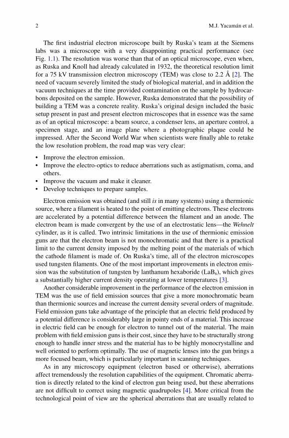
Fig. 1.1 Sketch by Ernst Ruska, dated 9 March 1931 of the cathode ray tube for testing one-stage and two-stage electro-optical imaging by means of two magnetic electron lenses (electron micro-scope). Source: Nobelprize.org Copyright © The Nobel Foundation (1986)
1 Aberration-Corrected Electron Microscopy of Nanoparticles
4
imperfections on the objective lens and may limit the resolution of the microscope to the degree of making atomistic resolution impossible. Some improvements were proposed to control spherical aberration in the 1950s, but the technology to truly avoid aberrations would not be developed until several decades later.
Vacuum may be a critical issue from two different standpoints. First, if a fieldemission source is being used, a way of avoiding contamination of the tip is to keep it operating in vacuum. Second, the path of the electron beam should be kept in vacuum to avoid the electrons to be scattered by the air molecules. Vacuum tech-niques have experienced great advances in the last decades, but even on the early stages of electron microscopy, the use of powerful mechanical pumps improved greatly the performance of the microscopes.
Simultaneously with the development of the instrument, the preparation of TEM specimens was refined. Samples were meticulously prepared using slicing and dim-pling techniques that allow to get thin areas that were basically transparent to the electron beam. Ion beam techniques were and still are used to remove contaminants from the sample’s surface.
By the mid-1950s, it was possible to design microscopes with a much betterresolution, clean vacuum, and better illumination using double condenser lenses. Probably the most significant discovery was the first direct observation of dislocation on a metal by Hirsh and its group (then at Cambridge). That was the culmination ofthe work of Orowan, Polanyi, and Taylor (who postulate the edge dislocations), of Burgers (that predicted the screw dislocation), and of Frank and Reed who pro-vided a mechanism to multiply dislocations [5]. The impact of these discoveries was monumental. In less than a half century, researchers were able to explain metallurgi-cal problems that had remained unsolved for more than 3,000 years. Thanks to those researchers metallurgy became truly a science and the mankind was now ready for developing new materials with “on-demand” properties. The amazing fact is that no big publicity was made on those discovering in contrast with the discoveries on quantum mechanics. No Nobel Prize was ever awarded on those discoveries. Laterin the mid-1960s, researchers had available very robust mechanics with a resolution better than 10 Å and with a great number of attachments such as goniometers, cold and heating stages, tensile stress stages, and so on. The preparation techniques were much improved. The theoretical foundations of image contrast were established, and it was possible for the first time to simulate electron microscope images.
By the mid-1980s, the resolution was improved to ~2 Å or better. It was possibleto obtain atomic column images under the right focusing conditions and for very thin specimens. The multislice theoretical approach of Cowley and Moodie [6] had opened the way to a serious comparison of experimental and theoretical images. Between 1970 and 1985, electron microscopy was used in many research areas, andthousands of materials and biological problems were solved using TEM. A lot of the rapid progress on electronic materials can be attributed to the availability of TEM.
Perhaps one of the most celebrated discoveries was the carbon nanotubes by Sumio Iijima [7] which was one of the detonators of nanotechnology. During the 1990s, the electron microscope became a powerful analytical machine. The intro-duction of field emission guns provided enough electron current for the X-ray anal-ysis (EDS) and the electron energy loss spectroscopy (EELS) to become standard
M.J. Yacamán et al.
5
techniques. They both save a great impulse to electron microscopy, and by the end of the century, electron microscopy and X-ray diffraction became the canonicaltechniques to characterize materials.
On the biological front, electron microscopy has been also a key technique. Backin 1665, the physicist Robert Hooke described the cells using an earlier optical microscope. That opened a brilliant era of discoveries using optical microscopes. After the discovery of the TEM, the impact has been very important. Practically all the cellular organelles (mitochondria, Golgi, vacuoles, and vesicles) were discov-ered using TEM. This was due to the staining methods of Claude and Palade plusthe development of ultramicrotoming. The use of TEM allowed the understanding of the functional organization of the cell and was a cornerstone of the development of modern cell biology. The development of cold stages and preparation methods resulted in the cryo-electron microscopy. This has been a fundamental technique to study viral ultrastructure. Combined with electron tomography, cryo-TEM hasshown how viral structural components fit together. The electron microscopy has been historically very important and has led to the discovery of new viruses such as the first image of polioviruses or the parvovirus, most intestinal virus, and very long list of others [8–11].
In the last few years, a quantum leap on the capabilities has unfolded mostly due to the development of aberration-corrected microscopy. We will describe it in the next few sections.
1.1.2 Aberration-Corrected Microscopy
In general, any optical instrument can be considered that transfers information from the object to a recording device (photographic plate or CCD or any other recordingdevice). If the transfer is perfect, we will have true information from the object. The final image can be magnified (microscope) or demagnified (telescope) or with no magnification (our eyes). In the case of our eyes, any physical deformity will lead to a blur on the image. In this case, we can easily correct all the aberrations of the eye by making a glass with that proper combination of divergent and convergent lenses. The same is true for the optical microscopes. In the case of the electron microscopy for almost 70 years, divergent lenses were not available. However, during the lastdecade of the twentieth century, there was a monumental advance on the electron optics, and hexapole and octupole lenses were available [12–14]. The key advance in modern microscopy is the aberration-corrected TEM and STEM.
One of the great minds of the twentieth century Richard P. Feynman said in his famous talk in 1959 in an American physical society meeting [15, 16]:
“The electron microscope is not quite good enough, with the greatest care and effort; it can only resolve about 10 angstroms. I would like to try and impress upon you while I am talk-ing about all of these things on a small scale, the importance of improving the electron microscope by a hundred times. It is not impossible; it is not against the laws of diffraction of the electron. The wavelength of the electron in such a microscope is only 1/20 of an
1 Aberration-Corrected Electron Microscopy of Nanoparticles
6
angstrom. So it should be possible to see the individual atoms. What good would it be to see individual atoms distinctly? We have friends in other fields—in biology, for instance. We physicists often look at them and say, “You should use more mathematics like we do.” They could answer us—but they’re polite, so I’ll answer for them: “What you should do in order for us to make more rapid progress is to make the electron microscope 100 times better and continued” The reason the electron microscope is so poor is that the f-value of the lenses is only 1 part to 1,000; you don’t have a big enough numerical aperture. And I know that there are theorems which prove that it is impossible, with axially symmetrical stationary field lenses, to produce an f-value any bigger so and so; and therefore the resolving power at the present time is at its theoretical maximum. But in every theorem there are assumptions.Why must the field be axially symmetrical? Why must the field be stationary? Can’t wehave pulsed electron beams in fields moving up along with the electrons? Must the field be symmetrical? I put this out as a challenge: Is there no way to make electron microscope more powerful?”
To meet the Feynman Challenge will mean to construct a microscope with aresolution of 0.1 Å or 10 pm. Commercial instruments have not reached the 50 pmlevel. It is not clear that it will be possible to reach the 10 pm, and some debate exists [17, 18]. However, it is clear that there are no materials with interatomic dis-tances <50 pm. That means that most (if not all) of the material science problems can be solved using a 50 pm resolution microscope. In the following sections are the physical principles of aberration correction.
1.1.3 TEM Aberration Correction
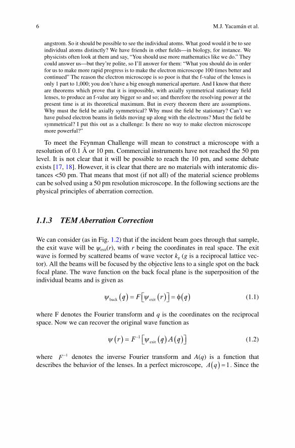
We can consider (as in Fig. 1.2) that if the incident beam goes through that sample, the exit wave will be ψexit(r), with r being the coordinates in real space. The exit wave is formed by scattered beams of wave vector kg (g is a reciprocal lattice vec-tor). All the beams will be focused by the objective lens to a single spot on the back focal plane. The wave function on the back focal plane is the superposition of the individual beams and is given as
ψ ψback exitq r q( ) = ( ) = ( )F φ
(1.1)
where F denotes the Fourier transform and q is the coordinates on the reciprocal space. Now we can recover the original wave function as
ψ ψr F q A q( ) = ( ) ( )
−1exit
(1.2)
where F −1 denotes the inverse Fourier transform and A(q) is a function that describes the behavior of the lenses. In a perfect microscope, A q( ) =1 . Since the
M.J. Yacamán et al.
7
product of two functions in Fourier space is equal to the convolution of the same two functions in real space, our final expression for the wave function is
ψ ψr r A r( ) = ( )⊗ ( )exit .
(1.3)
And the intensity on the image is
I r= ( )ψ
2.
(1.4)
This equation is independent of the approximation used for calculating the ψexit(r). Now we focus our attention in A(q). This function has been calculated for the case of coherent images as
t q
iqi ( ) = − ( )
exp2πλ
χ
(1.5)
Fig. 1.2 The information transfer diagram in an electron microscope
1 Aberration-Corrected Electron Microscopy of Nanoparticles
8
where
χ θ θq f C( ) = +
1
2
1
42 4
3∆
(1.6)
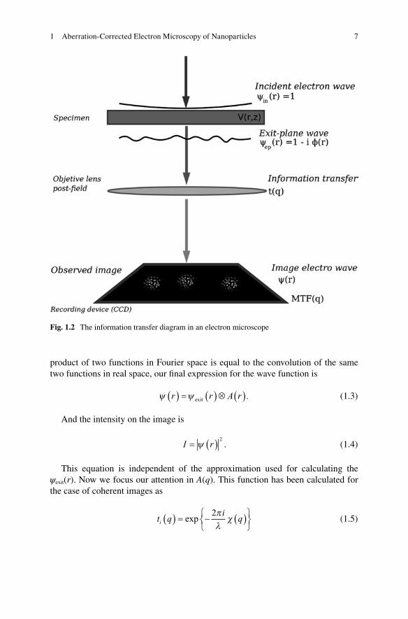
where Δf is the defocus and θ λ≈ q is the scattering angle, and C3 is the third-order spherical aberration. Equation (1.6) is valid when only isotropic aberration, defo-cus, and spherical aberration are present. However, if the microscope has an aberra-tion corrector, then, since C3 » 0, other aberration terms might become significant,such as the fifth-order spherical aberration; in a case like this, Eq. (1.5) would still be valid, but the function χ(q) should include a more general aberration function. In this case, additional axial aberrations need to be considered. The expression is much more complex, and if one takes up to the seventh order of aberration, we can have up to 44 coefficients which have to be taken into account including astigma-tism, spherical aberration, axial coma, and star, rosette, and chaplet aberration. For a full analysis, we refer the reader to the excellent book by Erni [19].
Figure 1.3 shows the plot of the χ function for different cases (corrected and uncorrected TEM) as a function of the scattering angle.
We can modify the equation χ, in the first approximation as
χ θ θ θq f C C( ) = + +
1
2
1
4
1
62 4
36
5∆
(1.7)
Fig. 1.3 Plot of the contrast transfer function χ for TEM. Different conditions corresponding to Scherzer condition for the corrected and uncorrected case and the Lentzen condition for the cor-rected case are shown
M.J. Yacamán et al.
9
where we have included the fifth-order spherical aberration C5. We have now a flex-ible situation. Even if C3 and C5 are zero, we can still get phase contrast with the defocus ±0. On the other hand, we can make C3 positive or negative, and we can adjust for different frequencies to be transferred. A particularly important condition for optimum contrast is the Scherzer focus for a corrected microscope which is given by (1.9):
∆f A C
C A C
Scherzer
Scherzer
=
= −
12
53
3 2 523
λ
λ.
(1.8)
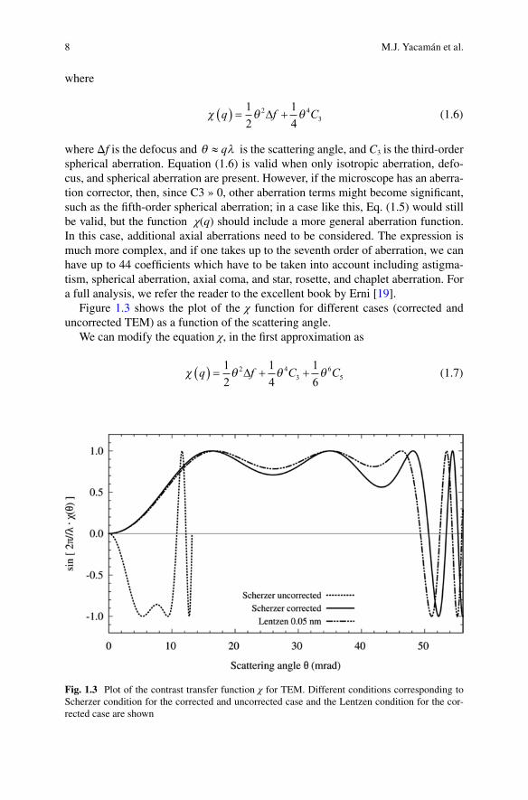
A1 and A2 are constants with the values around 2 and 3.2, respectively. Lentzen[20] has proposed a different set of values of the defocus. We have added in Fig. 1.2 the contrast transfer under Scherzer conditions in an aberration-corrected TEM. In any case, it is clear that aberration correction and the possibility of adjusting C3 and C5 give an extra capability to the microscope. An image of a corrected and uncor-rected Si crystal is shown in Fig. 1.4.
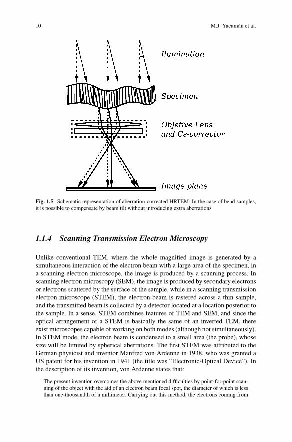
An additional important advantage of aberration-corrected TEM (shown in Fig. 1.5) is that in the case of bent samples, which is a common case due to sample preparation, it is possible to compensate by beam tilt without introducing extra aberrations.
Fig. 1.4 Image of an uncorrected (a) and corrected (b) Si crystal. Dumbbells separated at 1.3 Å in silicon [110]
1 Aberration-Corrected Electron Microscopy of Nanoparticles
10
1.1.4 Scanning Transmission Electron Microscopy
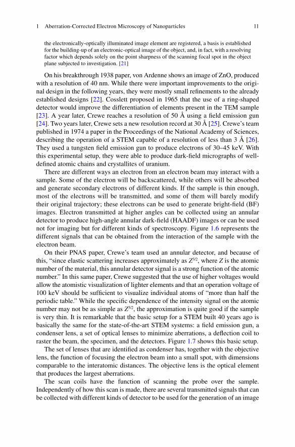
Unlike conventional TEM, where the whole magnified image is generated by asimultaneous interaction of the electron beam with a large area of the specimen, in a scanning electron microscope, the image is produced by a scanning process. In scanning electron microscopy (SEM), the image is produced by secondary electrons or electrons scattered by the surface of the sample, while in a scanning transmission electron microscope (STEM), the electron beam is rastered across a thin sample, and the transmitted beam is collected by a detector located at a location posterior to the sample. In a sense, STEM combines features of TEM and SEM, and since the optical arrangement of a STEM is basically the same of an inverted TEM, there exist microscopes capable of working on both modes (although not simultaneously). In STEM mode, the electron beam is condensed to a small area (the probe), whose size will be limited by spherical aberrations. The first STEM was attributed to the German physicist and inventor Manfred von Ardenne in 1938, who was granted a US patent for his invention in 1941 (the title was “Electronic-Optical Device”). Inthe description of its invention, von Ardenne states that:
The present invention overcomes the above mentioned difficulties by point-for-point scan-ning of the object with the aid of an electron beam focal spot, the diameter of which is less than one-thousandth of a millimeter. Carrying out this method, the electrons coming from
Fig. 1.5 Schematic representation of aberration-corrected HRTEM. In the case of bend samples, it is possible to compensate by beam tilt without introducing extra aberrations
M.J. Yacamán et al.
11
the electronically-optically illuminated image element are registered, a basis is established for the building-up of an electronic-optical image of the object, and, in fact, with a resolving factor which depends solely on the point sharpness of the scanning focal spot in the object plane subjected to investigation. [21]
On his breakthrough 1938 paper, von Ardenne shows an image of ZnO, produced with a resolution of 40 nm. While there were important improvements to the origi-nal design in the following years, they were mostly small refinements to the already established designs [22]. Cosslett proposed in 1965 that the use of a ring-shapeddetector would improve the differentiation of elements present in the TEM sample [23]. A year later, Crewe reaches a resolution of 50 Å using a field emission gun[24]. Two years later, Crewe sets a new resolution record at 30 Å [25]. Crewe’s teampublished in 1974 a paper in the Proceedings of the National Academy of Sciences,describing the operation of a STEM capable of a resolution of less than 3 Å [26]. They used a tungsten field emission gun to produce electrons of 30–45 keV. Withthis experimental setup, they were able to produce dark-field micrographs of well-defined atomic chains and crystallites of uranium.
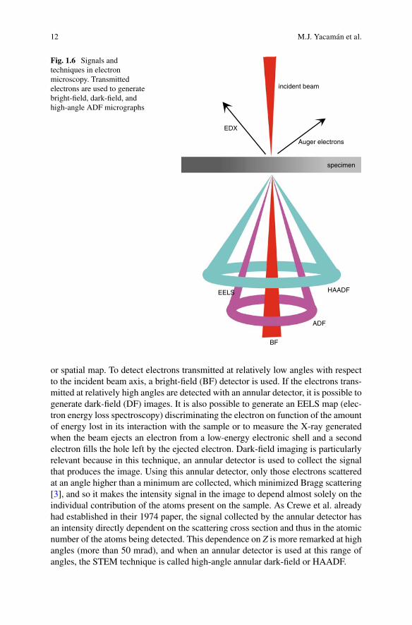
There are different ways an electron from an electron beam may interact with a sample. Some of the electron will be backscattered, while others will be absorbed and generate secondary electrons of different kinds. If the sample is thin enough, most of the electrons will be transmitted, and some of them will barely modify their original trajectory; these electrons can be used to generate bright-field (BF)images. Electron transmitted at higher angles can be collected using an annular detector to produce high-angle annular dark-field (HAADF) images or can be used not for imaging but for different kinds of spectroscopy. Figure 1.6 represents the different signals that can be obtained from the interaction of the sample with the electron beam.
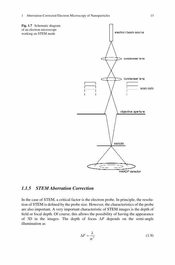
On their PNAS paper, Crewe’s team used an annular detector, and because ofthis, “since elastic scattering increases approximately as Z3/2, where Z is the atomic number of the material, this annular detector signal is a strong function of the atomic number.” In this same paper, Crewe suggested that the use of higher voltages wouldallow the atomistic visualization of lighter elements and that an operation voltage of 100 keV should be sufficient to visualize individual atoms of “more than half theperiodic table.” While the specific dependence of the intensity signal on the atomic number may not be as simple as Z3/2, the approximation is quite good if the sample is very thin. It is remarkable that the basic setup for a STEM built 40 years ago is basically the same for the state-of-the-art STEM systems: a field emission gun, a condenser lens, a set of optical lenses to minimize aberrations, a deflection coil to raster the beam, the specimen, and the detectors. Figure 1.7 shows this basic setup.
The set of lenses that are identified as condenser has, together with the objective lens, the function of focusing the electron beam into a small spot, with dimensions comparable to the interatomic distances. The objective lens is the optical element that produces the largest aberrations.
The scan coils have the function of scanning the probe over the sample. Independently of how this scan is made, there are several transmitted signals that can be collected with different kinds of detector to be used for the generation of an image
1 Aberration-Corrected Electron Microscopy of Nanoparticles
12
or spatial map. To detect electrons transmitted at relatively low angles with respect to the incident beam axis, a bright-field (BF) detector is used. If the electrons trans-mitted at relatively high angles are detected with an annular detector, it is possible to generate dark-field (DF) images. It is also possible to generate an EELS map (elec-tron energy loss spectroscopy) discriminating the electron on function of the amount of energy lost in its interaction with the sample or to measure the X-ray generatedwhen the beam ejects an electron from a low-energy electronic shell and a second electron fills the hole left by the ejected electron. Dark-field imaging is particularly relevant because in this technique, an annular detector is used to collect the signal that produces the image. Using this annular detector, only those electrons scatteredat an angle higher than a minimum are collected, which minimized Bragg scattering[3], and so it makes the intensity signal in the image to depend almost solely on the individual contribution of the atoms present on the sample. As Crewe et al. alreadyhad established in their 1974 paper, the signal collected by the annular detector hasan intensity directly dependent on the scattering cross section and thus in the atomic number of the atoms being detected. This dependence on Z is more remarked at high angles (more than 50 mrad), and when an annular detector is used at this range of angles, the STEM technique is called high-angle annular dark-field or HAADF.
specimen
incident beam
Auger electrons
EDX
HAADF
ADF
BF
EELS
Fig. 1.6 Signals and techniques in electron microscopy. Transmitted electrons are used to generate bright-field, dark-field, and high-angle ADF micrographs
M.J. Yacamán et al.
13
1.1.5 STEM Aberration Correction
In the case of STEM, a critical factor is the electron probe. In principle, the resolu-tion of STEM is defined by the probe size. However, the characteristics of the probe are also important. A very important characteristic of STEM images is the depth of field or focal depth. Of course, this allows the possibility of having the appearance of 3D in the images. The depth of focus ∆F depends on the semi-angle illumination as
∆F =
λα 2
(1.9)
Fig. 1.7 Schematic diagram of an electron microscope working on STEM mode
1 Aberration-Corrected Electron Microscopy of Nanoparticles
14
where λ is the wavelength. In the case of STEM, there is also influence of the aber-rations on the probe. Several aberrations affect the probe such as the STEM, the fourfold astigmatism, and the spherical aberration (C3 and C5). Again, there are optimum conditions for maximum contrast [27]:
∆f C
C C
= −
=−
1 56
2 88
25
3
3 523
.
..
λ
λ
(1.10)
These options show the critical importance of the C5 parameter. On the other hand, different factors play a role in an uncorrected STEM, such as the diffraction limit, the partial temporal coherence, the chromatic aberration Cc, and possible distur-bances of high frequency which alter the stability of the probe S5 noise. All those fac-tors are important to consider. However, the chromatic aberration and the spherical aberration are by far the most significant.
Another important factor is the depth of focus. For a noncorrected STEM oper-ated at 200 keV with a C3 1= mm and α =10mrad, the depth of focus is 25 nm, so a typical nanocrystal with ~100 atomic layers can be seen in focus. For an aberration- corrected STEM, the depth of focus radius is ~4 nm. That means that we can observe in focus ~18–20 atomic layers. This means that only small particles can be observed in focus. This on the other hand opens the possibility of focusing different thickness of the sample doing a kind of reconstruction similar to a confo-cal microscope.
In the next sections, we will use the case of nanoparticles for illustrating aberra-tion correction.
1.2 The Study of Clusters and Nanoparticles Using Aberration-Corrected Microscopy
1.2.1 Introduction
The study of nanoparticles with a nanometric size is one of the key aspects of nano-technology. Indeed, knowledge of the particle structure is fundamental to under-stand its properties. Nanoparticles can be studied at atomic level if a spherical aberration-corrected microscope is used. Modern mechanics can achieve resolu-tions around 70 pm in both objective lens-corrected (TEM) and probe-corrected(STEM) microscopes. However, the study of nanoparticles has several difficulties that should be addressed. In this chapter, we will discuss the methods to study nanoparticles.
M.J. Yacamán et al.
15
1.2.2 Difference Between Clusters and Nanoparticles
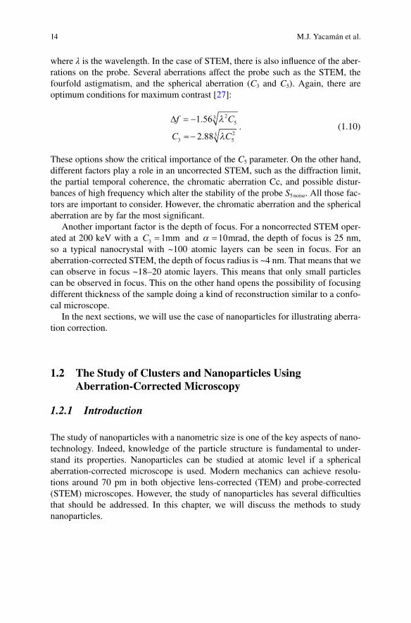
A very important distinction on the physical properties depends on the size of the nanoparticle. A first distinction should be when the particle has very few atoms. In this case, quantum effects are dominant, and it is better to call this particle a nano-cluster or a super-atom. When the number of atoms increases, the plasmonic effect starts to appear. The size at which setting of the plasmon resonance is produced should be considering the boundary between clusters and nanoparticles. This is illustrated in Fig. 1.8.
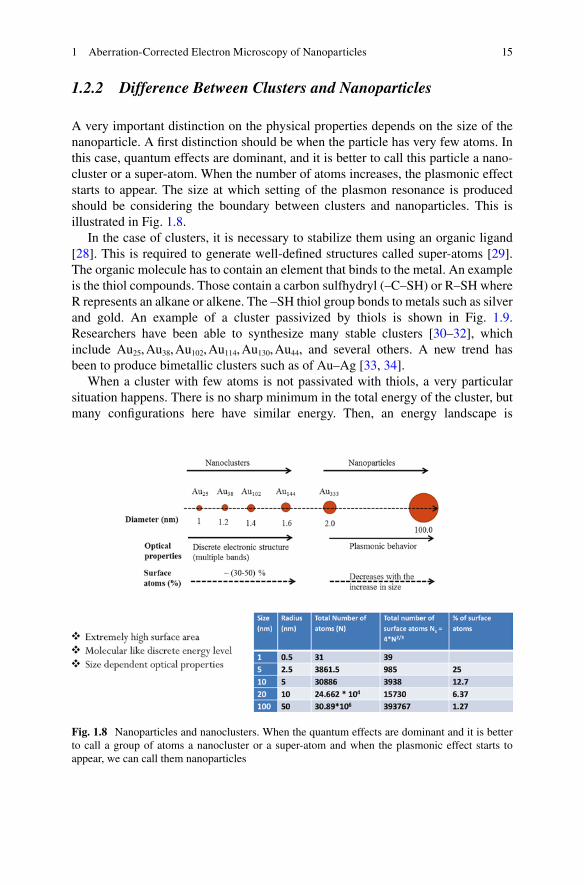
In the case of clusters, it is necessary to stabilize them using an organic ligand [28]. This is required to generate well-defined structures called super-atoms [29]. The organic molecule has to contain an element that binds to the metal. An example is the thiol compounds. Those contain a carbon sulfhydryl (–C–SH) or R–SH whereR represents an alkane or alkene. The –SH thiol group bonds to metals such as silver and gold. An example of a cluster passivized by thiols is shown in Fig. 1.9. Researchers have been able to synthesize many stable clusters [30–32], which include Au25, Au38, Au102, Au114, Au130, Au44, and several others. A new trend has been to produce bimetallic clusters such as of Au–Ag [33, 34].
When a cluster with few atoms is not passivated with thiols, a very particular situation happens. There is no sharp minimum in the total energy of the cluster, but many configurations here have similar energy. Then, an energy landscape is
Fig. 1.8 Nanoparticles and nanoclusters. When the quantum effects are dominant and it is better to call a group of atoms a nanocluster or a super-atom and when the plasmonic effect starts to appear, we can call them nanoparticles
1 Aberration-Corrected Electron Microscopy of Nanoparticles
16
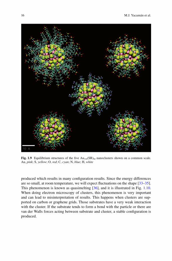
produced which results in many configuration results. Since the energy differences are so small, at room temperature, we will expect fluctuations on the shape [33–35]. This phenomenon is known as quasimelting [36], and it is illustrated in Fig. 1.10. When doing electron microscopy of clusters, this phenomenon is very important and can lead to misinterpretation of results. This happens when clusters are sup-ported on carbon or graphene grids. Those substrates have a very weak interaction with the cluster. If the substrate tends to form a bond with the particle or there are van der Walls forces acting between substrate and cluster, a stable configuration is produced.
Fig. 1.9 Equilibrium structures of the five Au144(SR)60 nanoclusters shown on a common scale. Au, pink; S, yellow; O, red; C, cyan; N, blue; H, white
M.J. Yacamán et al.
17
1.3 Radiation Damage in Clusters
STEM in probe correction microscopy is a fundamentally important technique to characterize clusters and nanoparticles since we can achieve atomic resolution. In addition, electron diffraction of clusters is in most instances kinematical which means that by measuring the intensities in at least two crystal axes, we can deter-mine the full crystal structure. The great advantage of electron diffraction is that no large crystals (as in the case of X-rays) are needed. In fact, nanocrystals can be
Fig. 1.10 Quasimelting observed in Au nanoparticles. The FFT corresponds to the particle on the left enclosed in a square. Every frame corresponds to 2 s elapsed time
1 Aberration-Corrected Electron Microscopy of Nanoparticles
18
easily diffracted. The number of passivized clusters whose structure has been deter-mined by X-rays is very limited. The reason is that not all clusters can be crystal-lized. Unfortunately, STEM, TEM, and electron diffraction have a great limitation,which is radiation damage. This may be the most important limiting factor that prevents obtaining reliable results. The main sources of radiation damage that affect the cluster or nanoparticle observation are radiolysis (or ionized) due to inelastic scattering and knock on, which is the displacement of atoms due to inelastic scatter-ing. The energy loss E suffered by primary electron may be transferred to a single atomic electron, which then undergoes a single-electron transition. In the case of a metal, the transition mostly involves conduction band electrons that are excited to empty states above the Fermi level Ef. A vacancy (hole) is produced in the valence band, which is filled very rapidly because of the high density of conduction elec-trons. This results in a temperature rise but no permanent damage. So the metal core is scarcely damaged by radiolysis. In the case of the organic capping, the situation is very difficult: transitions will produce electron–hole pairs, which are not filled fast. This might result in bond breaking, and also valence band electron might travel on the molecule producing more electron–hole pairs. Secondary electrons multiply the damage and eventually become the dominant source of radiolysis [37, 38]. It might also happen that the incoming electron excites an inner shell electron. In this case, the energy loss is much higher, and damage becomes considerable. When the core hole is filled with a valence electron, an Auger electron is released with the energy ~260 eV creating more bond damage. When the electron beamdestroys the passivating molecule, the cluster will be altered. It is well established in the case of nanoparticles that when particles are “naked,” instabilities are pro-duced by the electron beam as a result of the structure–composition relation.
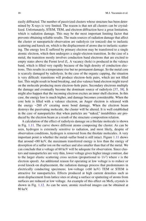
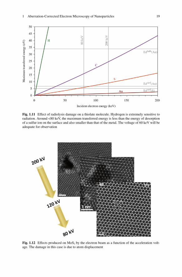
A calculation of the effect of radiolysis damage on a thiolate molecule is shown in Fig. 1.11. The curve shows different atoms composing the cluster. As can be seen, hydrogen is extremely sensitive to radiation, and most likely, despite of observation conditions, hydrogen is removed from the thiolate molecules. A very important point is whether the metal–sulfur bond is still intact. Figure 1.11 shows that around <80 keV, the maximum transferred energy is less than the energy ofdesorption of a sulfur ion on the surface and also smaller than that of the metal. We can conclude that a voltage of 60 keV will be adequate for observation. Since clus-ters and nanoparticles are very thin, lower voltage gives higher image contrast, due to the larger elastic scattering cross section (proportional to 1/v2) where v is the electron speed). An additional reason for operating at low voltage is to reduce or avoid knock-on displacement, the radiation damage process that predominates in electrically conducting specimens; low-voltage (<60 keV) TEM or STEM isattractive for nanoparticles. Effects produced at high current densities such as atom displacement from lattice sites or along a surface or sputtering of atoms from surfaces are reduced at low voltage. An example of this effect on MoS2 crystals is shown in Fig. 1.12. As can be seen, atomic resolved images can be obtained at 80 keV.
M.J. Yacamán et al.
19
Fig. 1.11 Effect of radiolysis damage on a thiolate molecule. Hydrogen is extremely sensitive to radiation. Around <80 keV, the maximum transferred energy is less than the energy of desorptionof a sulfur ion on the surface and also smaller than that of the metal. The voltage of 60 keV will beadequate for observation
Fig. 1.12 Effects produced on MoS2 by the electron beam as a function of the acceleration volt-age. The damage in this case is due to atom displacement
1 Aberration-Corrected Electron Microscopy of Nanoparticles
20
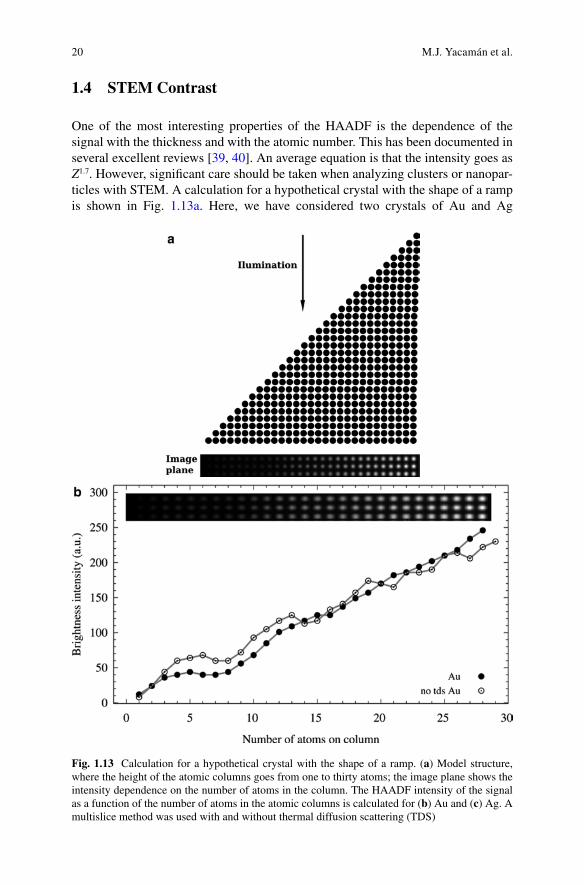
1.4 STEM Contrast
One of the most interesting properties of the HAADF is the dependence of the s ignal with the thickness and with the atomic number. This has been documented in several excellent reviews [39, 40]. An average equation is that the intensity goes as Z1.7. However, significant care should be taken when analyzing clusters or nanopar-ticles with STEM. A calculation for a hypothetical crystal with the shape of a ramp is shown in Fig. 1.13a. Here, we have considered two crystals of Au and Ag
Fig. 1.13 Calculation for a hypothetical crystal with the shape of a ramp. (a) Model structure, where the height of the atomic columns goes from one to thirty atoms; the image plane shows the intensity dependence on the number of atoms in the column. The HAADF intensity of the signal as a function of the number of atoms in the atomic columns is calculated for (b) Au and (c) Ag. A multislice method was used with and without thermal diffusion scattering (TDS)
M.J. Yacamán et al.
21
(Fig. 1.13a, b), and we have plotted the intensity of the signal as a function of the number of atoms in the atomic columns. We consider two cases, one with thermal diffuse scattering factoring and the other without. As can be seen, the intensity is linear up to five atoms; then there is a plateau and then an increase again. That means that a simple Z contrast analysis is valid for a particle of a diameter of 1.5 nm (assuming a spherical free particle). The same is valid for the case of Au. Of course, it is clear that a more involved calculation is necessary for setting an accurate atom counting [41, 42].
1.5 Radiation Damage in Nanoparticles
1.5.1 Small Nanoparticles
The boundary between cluster and nanoparticles is dependent of the type of metal (or semiconductor) forming the nanoparticle. However, the transition occurs sharply. In order to study the transition, we need to separate clusters size by size. In order to separate the clusters or nanoparticles, we used polyacrylamide gel electrophoresis (PAGE) using Tris–borate–EDTA (TBE) buffer (pH 8.0) in a Mini-PROTEAN GelElectrophoresis System (Bio-Rad). Separation and purification of Au nanoclusterscan be performed with 10 % PAGE gel using 2–5 μL of concentrated nanoclustersper well with 20 % v/v glycerol. Separation is performed at 110 V for 60 min or untilverification of formation of discrete bands. Sections corresponding to bands to dif-ferent nanoparticle sizes are recovered from PAGE gels by cutting with stainless
Fig. 1.13 (continued)
1 Aberration-Corrected Electron Microscopy of Nanoparticles
22
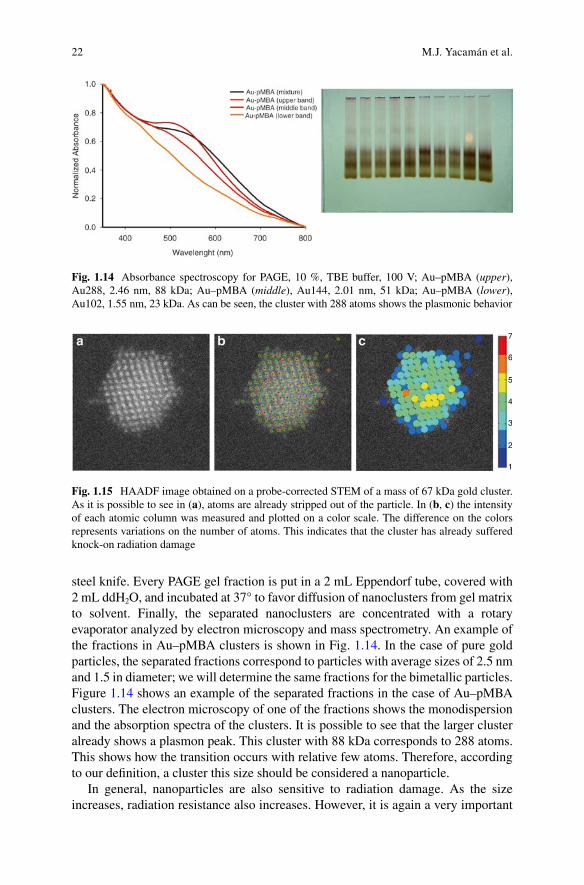
steel knife. Every PAGE gel fraction is put in a 2 mL Eppendorf tube, covered with2 mL ddH2O, and incubated at 37° to favor diffusion of nanoclusters from gel matrixto solvent. Finally, the separated nanoclusters are concentrated with a rotary evaporator analyzed by electron microscopy and mass spectrometry. An example of the fractions in Au–pMBA clusters is shown in Fig. 1.14. In the case of pure gold particles, the separated fractions correspond to particles with average sizes of 2.5 nm and 1.5 in diameter; we will determine the same fractions for the bimetallic particles. Figure 1.14 shows an example of the separated fractions in the case of Au–pMBAclusters. The electron microscopy of one of the fractions shows the monodispersion and the absorption spectra of the clusters. It is possible to see that the larger cluster already shows a plasmon peak. This cluster with 88 kDa corresponds to 288 atoms. This shows how the transition occurs with relative few atoms. Therefore, according to our definition, a cluster this size should be considered a nanoparticle.
In general, nanoparticles are also sensitive to radiation damage. As the size increases, radiation resistance also increases. However, it is again a very important
Fig. 1.14 Absorbance spectroscopy for PAGE, 10 %, TBE buffer, 100 V; Au–pMBA (upper), Au288, 2.46 nm, 88 kDa; Au–pMBA (middle), Au144, 2.01 nm, 51 kDa; Au–pMBA (lower), Au102, 1.55 nm, 23 kDa. As can be seen, the cluster with 288 atoms shows the plasmonic behavior
7
6
5
4
3
2
1
Fig. 1.15 HAADF image obtained on a probe-corrected STEM of a mass of 67 kDa gold cluster.As it is possible to see in (a), atoms are already stripped out of the particle. In (b, c) the intensity of each atomic column was measured and plotted on a color scale. The difference on the colors represents variations on the number of atoms. This indicates that the cluster has already suffered knock-on radiation damage
M.J. Yacamán et al.
23
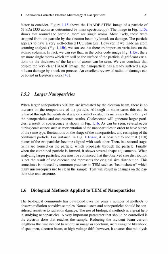
factor to consider. Figure 1.15 shows the HAADF-STEM image of a particle of 67 kDa (333 atoms as determined by mass spectroscopy). The image in Fig. 1.15a shows that around the particle, there are single atoms. Most likely, those were stripped from the particle by the electron beam by knock-on damage. The particle appears to have a very well-defined FCC structure. However, if we made an atomcounting analysis (Fig. 1.15b), we can see that there are important variations on the atomic columns. In fact, we can see that, in the color code image Fig. 1.15c, there are more single atoms which are still on the surface of the particle. Significant varia-tions on the thickness of the layers of atoms can be seen. We can conclude that despite the very clear HAADF image, the nanoparticle has already suffered a sig-nificant damage by knock-on process. An excellent review of radiation damage can be found in Egerton’s work [43].
1.5.2 Larger Nanoparticles
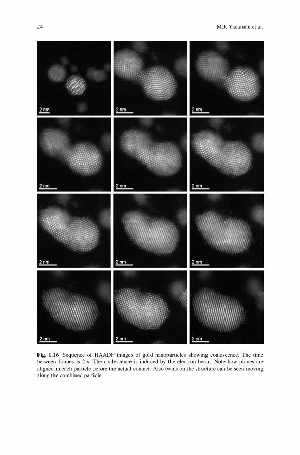
When larger nanoparticles >20 nm are irradiated by the electron beam, there is no increase on the temperature of the particle. Although in some cases this can be released through the substrate if a good contact exists, this increases the mobility of the nanoparticles and coalescence results. Coalescence will generate larger parti-cles; a result of coalescence is shown in Fig. 1.16. As can be seen, several occur during coalescence such as reorientation of the nanoparticles in order to have planes of the same type, fluctuations on the shape of the nanoparticles, and reshaping of the combined particle. For instance, in Fig. 1.16a–c, it is possible to see that ⟨110⟩ planes of the two particles become aligned with each other. Then, in a second stage, twins are formed on the particle, which propagate through the particle. Finally, when the combined particle is formed, it shows several shape adjustments. When analyzing larger particles, one must be convinced that the observed size distribution is not the result of coalescence and represents the original size distribution. This sometimes is induced by common practices in TEM such as “beam shower” which many microscopists use to clean the sample. That will result in changes on the par-ticle size and structure.
1.6 Biological Methods Applied to TEM of Nanoparticles
The biological community has developed over the years a number of methods to observe radiation-sensitive samples. Nanoclusters and nanoparticles should be con-sidered sensitive to radiation damage. The use of biological methods is a great help in studying nanoparticles. A very important parameter that should be controlled is the electron dose that reaches the sample. Reducing the incident beam current lengthens the time needed to record an image or spectrum, increasing the likelihood of specimen, electron beam, or high-voltage drift; however, it ensures that radiolysis
1 Aberration-Corrected Electron Microscopy of Nanoparticles
24
Fig. 1.16 Sequence of HAADF images of gold nanoparticles showing coalescence. The time between frames is 2 s. The coalescence is induced by the electron beam. Note how planes are aligned in each particle before the actual contact. Also twins on the structure can be seen moving along the combined particle
M.J. Yacamán et al.
25
will not be enhanced as a result of beam heating, and it reduces the risk of thermal decomposition or electrostatic charging effect. According to Egerton’s [43] calcula-tions, a dose rate less than 0.03 A/cm2 is required to minimize the electron beam heating. A total accumulated electron dose of ~0.01 C/cm2 will be required for clus-ter observation. In order to achieve a low dose, it is necessary to use a CMOS-basedcamera on the TEM. CMOS architecture uses lowest noise sensors resulting in highdynamic range (>10,000:1) and single-electron sensitivity and a very low dose.
In addition [43], the mass loss (and structural damage) can be reduced by cooling the specimen with liquid nitrogen. Under these conditions, it might be expected thatdamage would also depend on the irradiation time. Dose rate as well as the accumu-lated dose delivering the electrons in a time shorter than that required for significant diffusion might produce less mass loss; therefore, cryomicroscopy is very conve-nient for cluster structure analysis. In most cases, liquid nitrogen cooling is enough to study clusters.
In a recent paper, Azubel et al. [44] studied the monometallic cluster Au69(SR)x using a very similar concept to the one described in this proposal. They use cryo- TEM and standard low-dose methods. A major difference is that they used bright- field image averaging 939 particles acquired in this which was processed with the EMAN2 software package [45] which yielded an electron density map with 68 peaks. From that map, the authors reconstruct the structure. This work is a fine example of the use of biological methods in cluster research.
1.7 Nanodiffraction of Nanoparticles
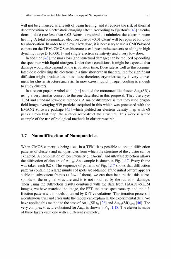
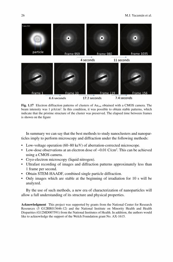
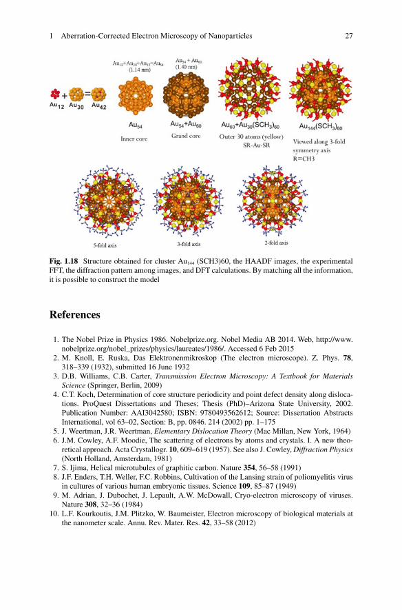
When CMOS camera is being used in a TEM, it is possible to obtain diffractionpatterns of clusters and nanoparticles from which the structure of the cluster can be extracted. A combination of low intensity (1 pA/cm2) and ultrafast detection allows the diffraction of clusters of Au144. An example is shown in Fig. 1.17. Every frame was taken each 0.2 s. The sequence of patterns of Fig. 1.17 shows that diffraction patterns containing a large number of spots are obtained. If the initial pattern appears stable in subsequent frames (a few of them), we can then be sure that this corre-sponds to the original structure and it is not modified by the radiation damage. Then using the diffraction results combined with the data from HAADF-STEM images, we have matched the image, the FFT, the mass spectrometry, and the dif-fraction pattern with models obtained by DFT calculations. This iteration process is a continuous trial and error until the model can explain all the experimental data. We have applied this method to the case of Au144(SR)60 [26] and Au130(SR)50/80 [46]. The very complex structure obtained for Au144 is shown in Fig. 1.18. The cluster is made of three layers each one with a different symmetry.
1 Aberration-Corrected Electron Microscopy of Nanoparticles
26
In summary we can say that the best methods to study nanoclusters and nanopar-ticles imply to perform microscopy and diffraction under the following methods:
• Low-voltage operation (60–80 keV) of aberration-corrected microscope.• Low-dose observations at an electron dose of ~0.01 C/cm2. This can be achieved
using a CMOS camera.• Cryo-electron microscopy (liquid nitrogen).• Ultrafast recording of images and diffraction patterns approximately less than
1 frame per second.• Obtain STEM-HAADF, combined single particle diffraction.• Only images which are stable at the beginning of irradiation for 10 s will be
analyzed.
By the use of such methods, a new era of characterization of nanoparticles willallow a full understanding of its structure and physical properties.
Acknowledgment This project was supported by grants from the National Center for ResearchResources (5 G12RR013646-12) and the National Institute on Minority Health and Health Disparities (G12MD007591) from the National Institutes of Health. In addition, the authors wouldlike to acknowledge the support of the Welch Foundation grant No. AX-1615.
Fig. 1.17 Electron diffraction patterns of clusters of Au144 obtained with a CMOS camera. Thebeam intensity was 1 pA/cm2. In this condition, it was possible to obtain stable patterns, which indicate that the pristine structure of the cluster was preserved. The elapsed time between frames is shown on the figure
M.J. Yacamán et al.
27
References
1. The Nobel Prize in Physics 1986. Nobelprize.org. Nobel Media AB 2014. Web, http://www.nobelprize.org/nobel_prizes/physics/laureates/1986/. Accessed 6 Feb 2015
2. M. Knoll, E. Ruska, Das Elektronenmikroskop (The electron microscope). Z. Phys. 78, 318–339 (1932), submitted 16 June 1932
3. D.B. Williams, C.B. Carter, Transmission Electron Microscopy: A Textbook for Materials Science (Springer, Berlin, 2009)
4. C.T. Koch, Determination of core structure periodicity and point defect density along disloca-tions. ProQuest Dissertations and Theses; Thesis (PhD)–Arizona State University, 2002.Publication Number: AAI3042580; ISBN: 9780493562612; Source: Dissertation AbstractsInternational, vol 63–02, Section: B, pp. 0846. 214 (2002) pp. 1–175
5. J. Weertman, J.R. Weertman, Elementary Dislocation Theory (Mac Millan, New York, 1964)6. J.M. Cowley, A.F. Moodie, The scattering of electrons by atoms and crystals. I. A new theo-
retical approach. Acta Crystallogr. 10, 609–619 (1957). See also J. Cowley, Diffraction Physics (North Holland, Amsterdam, 1981)
7. S. Ijima, Helical microtubules of graphitic carbon. Nature 354, 56–58 (1991)8. J.F. Enders, T.H. Weller, F.C. Robbins, Cultivation of the Lansing strain of poliomyelitis virus
in cultures of various human embryonic tissues. Science 109, 85–87 (1949)9. M. Adrian, J. Dubochet, J. Lepault, A.W. McDowall, Cryo-electron microscopy of viruses.
Nature 308, 32–36 (1984)10. L.F. Kourkoutis, J.M. Plitzko, W. Baumeister, Electron microscopy of biological materials at
the nanometer scale. Annu. Rev. Mater. Res. 42, 33–58 (2012)
Fig. 1.18 Structure obtained for cluster Au144 (SCH3)60, the HAADF images, the experimentalFFT, the diffraction pattern among images, and DFT calculations. By matching all the information,it is possible to construct the model
1 Aberration-Corrected Electron Microscopy of Nanoparticles
28
11. P.W. Hawkes (ed.), Advances in Imaging and Electron Physics, vol 182 (Academic Press, San Diego, 2014), pp. 1–94
12. A. Howie, Aberration correction: zooming out to overview. Phil. Trans. R. Soc. A 367, 3859–3870 (2009)
13. H.H. Rose, Historical aspects of aberration correction. J. Electron Microsc. 58, 77–85 (2009) 14. P.W. Hawkes, Aberration correction past and present. Phil. Trans. R. Soc. A 367, 3637–3664
(2009) 15. Richard Feynman gave a classical talk on December 29th 1959 at the annual meeting of the
American Physical Society at the California Institute of Technology (Caltech) was first pub-lished in Caltech Engineering and Science, vol 23, 5 Feb 1960, pp 22–36. It has been madeavailable on the web at http://www.zyvex.com/nanotech/feynman.html with their kind permis-sion. The scanned original is available
16. E.S. Reich, Imaging hits noise barrier. Nature 499, 135–136 (2013)17. S. Ulemann, H. Müller, P. Hartel, J. Zach, M. Haider, Thermal magnetic field noise limits reso-
lution in transmission electron microscopy. Phys. Rev. Lett. 111, 046101 (2013)18. S.J. Pennycook, S.V. Kalinin, Microscopy: Hasten high resolution. Nature 515, 487–488
(2014) 19. R. Erni, Aberration Corrected Imaging in Transmission Electron Microscopy: An Introduction
(Imperial College Press, London, 2010)20. M. Lentzen, Contrast transfer and resolution limits for sub-angstrom high-resolution transmis-
sion electron microscopy. Microsc. Microanal. 14, 16–26 (2008)21. M. von Ardenne, Electronic-optical device. U.S. Patent 2,257,774, filed 15 Feb 1938, and
issued 7 Oct 194122. M. von Ardenne, Das Elektronen-Rastermikroskop. Praktische Ausführung. Z. Tech. Phys. 19,
407–416, as reproduced in S.J. Pennycook, P.D. Nellist, Scanning Transmission Electron Microscopy: Imaging and Analysis (Springer, New York, 2011)
23. V.E. Cosslett, Possibilities and limitations for the differentiation of elements in the electronmicroscope. Lab. Invest. 14, 1009–1019 (1965)
24. A.V. Crewe, Scanning electron microscopes: is high resolution possible? Science 154(3750),729–738 (1966)
25. A.V. Crewe, J. Wall, L.M. Welter, A high‐resolution scanning transmission electron micro-scope. J. Appl. Phys. 39(13), 5861–5868 (1968)
26. J. Wall et al., Scanning transmission electron microscopy at high resolution. Proc. Natl. Acad. Sci. U. S. A. 71(1), 1–5 (1974)
27. L.Y. Chang, A.I. Kirkland, J.M. Titchmarsh, On the importance of fifth-order spherical aberra-tion for a fully corrected electron microscope. Ultramicroscopy 106, 301–306 (2006)
28. M.M. Alvarez, J.T. Khoury, T.G. Schaaff, M.N. Shafigullin, I. Vezmar, R.L. Whetten, Opticalabsorption spectra of nanocrystal gold molecules. J. Phys. Chem. B 101, 3706–3712 (1997)
29. M. Walter, J. Akola, O. Lopez-Acevedo, P.D. Jadzinsky, G. Calero, C.J. Ackerson,R.L. Whetten, H. Gronbeck, H. Hakkinen, A unified view of ligand-protected gold clusters assuperatom complexes. Proc. Natl. Acad. Sci. U. S. A. 105, 9157–9162 (2008)
30. A. Dass, P. Ninmala, V. Jupally, N. Kothalawa, Au103(SR)45, Au104(SR)45, Au104(SR)46 and Au105(SR)46 nanoclusters. Nanoscale 5, 12082–12085 (2013)
31. A. Dass, Nano-scaling law: geometric foundation of thiolated gold nanomolecules. Nanoscale 4, 2260–2263 (2012)
32. Y. Negishi, N.K. Chaki, Y. Shichibu, R.L. Whetten, T. Tsukuda, Origin of magic stability ofthiolated gold clusters: a case study on Au25(SC6H13)18. J. Am. Chem. Soc. 129, 11322–11323 (2007)
33. C. Kumara, C.M. Aikens, A. Dass, X-ray crystal structure and theoretical analysis of Au25–
xAgx(SCH2CH2Ph)18–alloy. J. Phys. Chem. Lett. 5, 461–466 (2014)34. W. Krakow, M. Jóse-Yacamán, J.L. Aragón, Observation of quasimelting at the atomic level in
Au nanoclusters. Phys. Rev. B 49, 10591–10596 (1994)
M.J. Yacamán et al.
29
35. D.J. Smith, A.K. Petford-Long, L.R. Wallenberg, J.O. Bovin, Dynamic atomic-level rearrangements in small gold particles. Science 233, 872–875 (1986)
36. P.M. Ajayan, L.D. Marks, Experimental evidence for quasimelting in small particles. Phys.Rev. Lett. 63, 279–282 (1989)
37. R.F. Egerton, F. Wang, P.A. Crozier, Beam-induced damage to thin specimens in an intenseelectron probe. Microsc. Microanal. 12, 65–71 (2006)
38. M. Malac, M. Beleggia, R. Egerton, Y. Zhu, Bright-field TEM imaging of single molecules:dream or near future? Ultramicroscopy 107, 40–49 (2007)
39. G. van Tendeloo, S. Bals, S. Van Aert, J. Verbeeck, D. van Dyck, Advanced electron micros-copy for advanced materials. Adv. Mater. 24, 5655–5675 (2012)
40. S.J. Pennycock, P.D. Nelist (eds.), Scanning Transmission Electron Microscopy: Imaging and Analysis (Springer, New York, 2011), p. 762
41. A. De Backer, G. Martinez, A. Rosenauer, S. Van Aert, Atom counting in HAADF STEMusing a statistical model-based approach: methodology, possibilities, and inherent limitations. Ultramicroscopy 134, 23–33 (2013)
42. J.M. LeBeau, S.D. Findlay, L.J. Allen, S. Stemmer, Standardless atom counting in scanningtransmission electron microscopy. Nano Lett. 10, 4405–4408 (2010)
43. R. Egerton, Control of radiation damage in the TEM. Ultramicroscopy 127, 100–108 (2013)44. M. Azubel, J. Koivisto, S. Malola, D. Bushnell, G.L. Hura, A.L. Koh, H. Tsunoyama,
T. Tsukuda, M. Pettersson, H. Häkkinen, Electron microscopy of gold nanoparticles at atomic resolution. Science 345, 909–912 (2014)
45. G. Tang, L. Peng, P.R. Baldwin, D.S. Mann, W. Jiang, I. Rees, S.J. Ludtke, EMAN2: an exten-sible image processing suite for electron microscopy. J. Struct. Biol. 157, 38–46 (2007)
46. D. Bahena, N. Bhattarai, U. Santiago, A. Tlahuice, A. Ponce, S.B. Bach, B. Yoon, R.L. Whetten,U. Landman, M. Jose-Yacaman, STEM electron diffraction and high-resolution images usedin the determination of the crystal structure of the Au144(SR)60 cluster. J. Phys. Chem. Lett. 4, 975–981 (2013)
1 Aberration-Corrected Electron Microscopy of Nanoparticles