Embed Size (px)
Citation preview
36 MRS BULLETIN • VOLUME 31 • JANUARY 2006
IntroductionRichard Feynman is widely associated
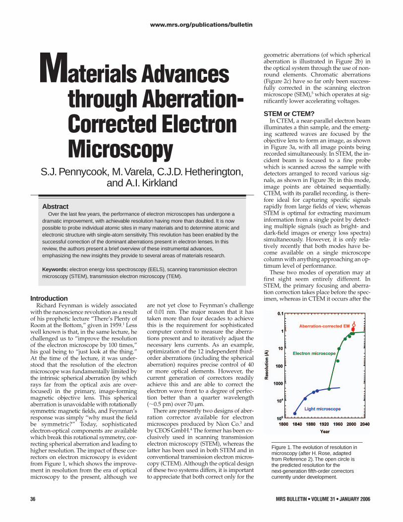
with the nanoscience revolution as a resultof his prophetic lecture “There’s Plenty ofRoom at the Bottom,” given in 1959.1 Lesswell known is that, in the same lecture, hechallenged us to “improve the resolutionof the electron microscope by 100 times,”his goal being to “just look at the thing.”At the time of the lecture, it was under-stood that the resolution of the electronmicroscope was fundamentally limited bythe intrinsic spherical aberration (by whichrays far from the optical axis are over-focused) in the primary, image-formingmagnetic objective lens. This sphericalaberration is unavoidable with rotationallysymmetric magnetic fields, and Feynman’sresponse was simply “why must the fieldbe symmetric?” Today, sophisticatedelectron-optical components are availablewhich break this rotational symmetry, cor-recting spherical aberration and leading tohigher resolution. The impact of these cor-rectors on electron microscopy is evidentfrom Figure 1, which shows the improve-ment in resolution from the era of opticalmicroscopy to the present, although we
are not yet close to Feynman’s challengeof 0.01 nm. The major reason that it hastaken more than four decades to achievethis is the requirement for sophisticatedcomputer control to measure the aberra-tions present and to iteratively adjust thenecessary lens currents. As an example,optimization of the 12 independent third-order aberrations (including the sphericalaberration) requires precise control of 40or more optical elements. However, thecurrent generation of correctors readilyachieve this and are able to correct theelectron wave front to a degree of perfec-tion better than a quarter wavelength(�0.5 pm) over 70 µm.
There are presently two designs of aber-ration corrector available for electronmicroscopes produced by Nion Co.3 andby CEOS GmbH.4 The former has been ex-clusively used in scanning transmissionelectron microscopy (STEM), whereas thelatter has been used in both STEM and inconventional transmission electron micros-copy (CTEM). Although the optical designof these two systems differs, it is importantto appreciate that both correct only for the
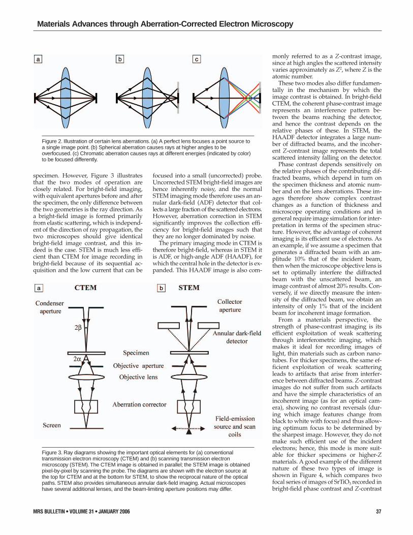
geometric aberrations (of which sphericalaberration is illustrated in Figure 2b) inthe optical system through the use of non-round elements. Chromatic aberrations(Figure 2c) have so far only been success-fully corrected in the scanning electronmicroscope (SEM),5 which operates at sig-nificantly lower accelerating voltages.
STEM or CTEM?In CTEM, a near-parallel electron beam
illuminates a thin sample, and the emerg-ing scattered waves are focused by the objective lens to form an image, as shownin Figure 3a, with all image points beingrecorded simultaneously. In STEM, the in-cident beam is focused to a fine probewhich is scanned across the sample withdetectors arranged to record various sig-nals, as shown in Figure 3b; in this mode,image points are obtained sequentially.CTEM, with its parallel recording, is there-fore ideal for capturing specific signalsrapidly from large fields of view, whereasSTEM is optimal for extracting maximuminformation from a single point by detect-ing multiple signals (such as bright- anddark-field images or energy loss spectra)simultaneously. However, it is only rela-tively recently that both modes have be-come available on a single microscopecolumn with anything approaching an op-timum level of performance.
These two modes of operation may atfirst sight seem entirely different. InSTEM, the primary focusing and aberra-tion correction takes place before the spec-imen, whereas in CTEM it occurs after the
Materials Advancesthrough Aberration-Corrected ElectronMicroscopy
S.J. Pennycook, M.Varela, C.J.D. Hetherington,and A.I. Kirkland
AbstractOver the last few years, the performance of electron microscopes has undergone a
dramatic improvement, with achievable resolution having more than doubled. It is nowpossible to probe individual atomic sites in many materials and to determine atomic andelectronic structure with single-atom sensitivity.This revolution has been enabled by thesuccessful correction of the dominant aberrations present in electron lenses. In thisreview, the authors present a brief overview of these instrumental advances,emphasizing the new insights they provide to several areas of materials research.
Keywords: electron energy loss spectroscopy (EELS), scanning transmission electronmicroscopy (STEM), transmission electron microscopy (TEM).
Figure 1.The evolution of resolution inmicroscopy (after H. Rose, adaptedfrom Reference 2).The open circle isthe predicted resolution for thenext-generation fifth-order correctorscurrently under development.
www.mrs.org/publications/bulletin
Materials Advances through Aberration-Corrected Electron Microscopy
MRS BULLETIN • VOLUME 31 • JANUARY 2006 37
specimen. However, Figure 3 illustratesthat the two modes of operation areclosely related. For bright-field imaging,with equivalent apertures before and afterthe specimen, the only difference betweenthe two geometries is the ray direction. Asa bright-field image is formed primarilyfrom elastic scattering, which is independ-ent of the direction of ray propagation, thetwo microscopes should give identicalbright-field image contrast, and this in-deed is the case. STEM is much less effi-cient than CTEM for image recording inbright-field because of its sequential ac-quisition and the low current that can be
focused into a small (uncorrected) probe.Uncorrected STEM bright-field images arehence inherently noisy, and the normalSTEM imaging mode therefore uses an an-nular dark-field (ADF) detector that col-lects a large fraction of the scattered electrons.However, aberration correction in STEMsignificantly improves the collection effi-ciency for bright-field images such thatthey are no longer dominated by noise.
The primary imaging mode in CTEM istherefore bright-field, whereas in STEM itis ADF, or high-angle ADF (HAADF), forwhich the central hole in the detector is ex-panded. This HAADF image is also com-
monly referred to as a Z-contrast image,since at high angles the scattered intensityvaries approximately as Z2, where Z is theatomic number.
These two modes also differ fundamen-tally in the mechanism by which theimage contrast is obtained. In bright-fieldCTEM, the coherent phase-contrast imagerepresents an interference pattern be-tween the beams reaching the detector,and hence the contrast depends on the relative phases of these. In STEM, theHAADF detector integrates a large num-ber of diffracted beams, and the incoher-ent Z-contrast image represents the totalscattered intensity falling on the detector.
Phase contrast depends sensitively onthe relative phases of the contributing dif-fracted beams, which depend in turn onthe specimen thickness and atomic num-ber and on the lens aberrations. These im-ages therefore show complex contrastchanges as a function of thickness andmicroscope operating conditions and ingeneral require image simulation for inter-pretation in terms of the specimen struc-ture. However, the advantage of coherentimaging is its efficient use of electrons. Asan example, if we assume a specimen thatgenerates a diffracted beam with an am-plitude 10% that of the incident beam,then when the microscope objective lens isset to optimally interfere the diffractedbeam with the unscattered beam, animage contrast of almost 20% results. Con-versely, if we directly measure the inten-sity of the diffracted beam, we obtain anintensity of only 1% that of the incidentbeam for incoherent image formation.
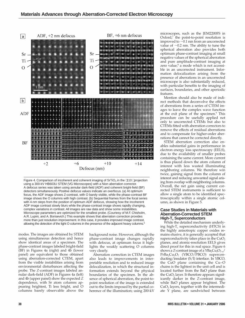
From a materials perspective, thestrength of phase-contrast imaging is itsefficient exploitation of weak scatteringthrough interferometric imaging, whichmakes it ideal for recording images oflight, thin materials such as carbon nano-tubes. For thicker specimens, the same ef-ficient exploitation of weak scatteringleads to artifacts that arise from interfer-ence between diffracted beams. Z-contrastimages do not suffer from such artifactsand have the simple characteristics of anincoherent image (as for an optical cam-era), showing no contrast reversals (dur-ing which image features change fromblack to white with focus) and thus allow-ing optimum focus to be determined bythe sharpest image. However, they do notmake such efficient use of the incidentelectrons; hence, this mode is more suit-able for thicker specimens or higher-Zmaterials. A good example of the differentnature of these two types of image isshown in Figure 4, which compares twofocal series of images of SrTiO3 recorded inbright-field phase contrast and Z-contrast
Figure 2. Illustration of certain lens aberrations. (a) A perfect lens focuses a point source toa single image point. (b) Spherical aberration causes rays at higher angles to beoverfocused. (c) Chromatic aberration causes rays at different energies (indicated by color)to be focused differently.
Figure 3. Ray diagrams showing the important optical elements for (a) conventionaltransmission electron microscopy (CTEM) and (b) scanning transmission electron microscopy (STEM).The CTEM image is obtained in parallel; the STEM image is obtainedpixel-by-pixel by scanning the probe.The diagrams are shown with the electron source atthe top for CTEM and at the bottom for STEM, to show the reciprocal nature of the opticalpaths. STEM also provides simultaneous annular dark-field imaging. Actual microscopeshave several additional lenses, and the beam-limiting aperture positions may differ.
38 MRS BULLETIN • VOLUME 31 • JANUARY 2006
Materials Advances through Aberration-Corrected Electron Microscopy
modes. The images are obtained by STEMusing simultaneous detection and henceshow identical areas of a specimen. Thephase-contrast images labeled bright-field(BF) in Figures 4a (right) and 4b (lowerpanel) are equivalent to those obtainedusing aberration-corrected CTEM, apartfrom the visible instabilities arising fromenvironmental disturbances affecting theprobe. The Z-contrast images labeled an-nular dark-field (ADF) in Figures 4a (left)and 4b (upper panel) show the expected Zdependence, with Sr atom columns ap-pearing brightest, Ti less bright, and Ocolumns barely observable above the
background noise. However, although thephase-contrast image changes rapidlywith defocus, at optimum focus it high-lights the weakly scattering O columnsvery clearly.
Aberration correction in CTEM imagesalso leads to improvements in inter-pretable resolution and to reduced imagedelocalization, in which the structural in-formation extends beyond the physicalboundaries of the specimen. In the ab-sence of spherical aberration, the point-to-point resolution of the image is extendedout to the limits imposed by the partial co-herence of the illumination; using 200-kV
microscopes, such as the JEM2200FS inOxford,7 the point-to-point resolution isimproved to �0.1 nm from an uncorrectedvalue of �0.2 nm. The ability to tune thespherical aberration also provides bothoptimum phase-contrast imaging at smallnegative values of the spherical aberrationand pure amplitude-contrast imaging atzero value,8 a mode which is not accessi-ble in an uncorrected instrument. Infor-mation delocalization arising from thepresence of aberrations in an uncorrectedmicroscope is also substantially reduced,with particular benefits to the imaging ofsurfaces, boundaries, and other aperiodicfeatures.
Mention should also be made of indi-rect methods that deconvolve the effectsof aberrations from a series of CTEM im-ages to leave the complex wave functionat the exit plane of the specimen.9 Thisprocedure can be usefully applied notonly to uncorrected CTEMs but also toCTEMs fitted with aberration correctors toremove the effects of residual aberrationsand to compensate for higher-order aber-rations that cannot be corrected directly.
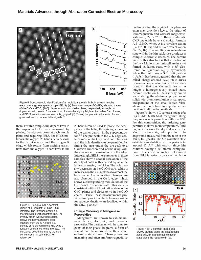
STEM aberration correction also en-ables substantial gains in performance inelectron energy loss spectroscopy (EELS),due to the availability of smaller probescontaining the same current. More currentis thus placed down the atom column ofinterest with less wasted illuminatingneighboring columns. We therefore wintwice, gaining signal from the column ofinterest and reducing unwanted signal aris-ing from overlap with neighboring columns.Overall, the net gain using current cor-rected STEM instruments is sufficient toallow a single atom to be identified spec-troscopically within a single atomic col-umn, as shown in Figure 5.
Case Studies in Materials withAberration-Corrected STEMHigh-Tc Superconductors
While the detailed mechanism underly-ing high-Tc superconductivity (HTCS) inthe highly anisotropic copper oxides re-mains elusive, it is generally accepted thatsuperconductivity takes place in the CuO2planes, and atomic-resolution EELS givesdirect proof for this in real space. Figure 6shows a Z-contrast image of a YBa2Cu3O7–x/PrBa2Cu3O7 (YBCO/PBCO) supercon-ducting/insulator (S/I) interface. In YBCO,the CuO plane containing the Cu–Ochains is the lightest in the unit cell and islocated further from the BaO plane thanthe CuO2 layer. It therefore appears signif-icantly darker in the Z-contrast image,while BaO planes appear brightest. TheCuO2 layers, together with the intermedi-ate Y plane, are sandwiched between
Figure 4. Comparison of incoherent and coherent imaging of SrTiO3 in the ⟨110 ⟩ projectionusing a 300-kV HB603U STEM (VG Microscopes) with a Nion aberration corrector.A defocus series was taken using annular dark-field (ADF) and coherent bright-field (BF)detectors simultaneously. Positive defocus values indicate an overfocus. (a) At optimumfocus, the ADF image shows Z-contrast, with O barely visible, while the phase-contrast BFimage shows the O columns with high contrast. (b) Sequential frames from the focal serieswith 4-nm steps from the position of optimum ADF defocus, showing how the incoherentADF image contrast slowly blurs while the phase-contrast image shows rapidly changing,complex variations in contrast. All images are raw data and show some instabilities.Microscope parameters are optimized for the smallest probe. (Courtesy of M.F. Chisholm,A.R. Lupini, and A. Borisevich.) This example shows that aberration correction providesmore than just resolution improvement. In this case, it provides improved image contrast,allowing the detection of the light O columns in the presence of the adjacent heavy columns.6
Materials Advances through Aberration-Corrected Electron Microscopy
MRS BULLETIN • VOLUME 31 • JANUARY 2006 39
them. For this sample, the dopant level inthe superconductor was measured byplacing the electron beam at each atomicplane and acquiring EELS. For HTCS ma-terials, the oxygen 2p bands lie very closeto the Fermi energy, and the oxygen Kedge, which results from exciting transi-tions from the oxygen 1s core level to the
2p bands, can be used to probe the occu-pancy of the latter, thus giving a measureof the carrier density in the superconduc-tor.11,12 The pre-peak in the O K edge con-tains most of the O 2p band contributions,and the hole density can be quantified byfitting the area under the pre-peak to aGaussian function and normalizing withthe area under the main body of the edge.Interestingly, EELS measurements in thesesamples show a spatial oscillation of thedensity of holes with a period equal to thelattice parameter, c � 11.7 Å. The hole den-sity decreases on the CuO chains, while itincreases on the CuO2 planes to almost thebulk value. Corresponding changes arealso observed in the Cu L edge, whichshows a corresponding modulation of theCu formal oxidation state. This data isconsistent with a �2 oxidation state in theCuO2 planes and closer to �1 in the CuOchains. Hence, these measurements pro-vide direct proof that the holes responsiblefor superconductivity are localized withinthe CuO2 planes.13
Charge Ordering in ManganesePerovskites
Manganites are known to exhibit un-usual lattice, electronic, and magneticproperties.14 In particular, within some re-gions of their phase diagrams, a form ofspatial modulation known as the charge-ordered state is found. These phases areinsulating and often antiferromagnetic, so
understanding the origin of this phenom-enon may provide a key to the origin offerromagnetism and colossal magnetore-sistance (CMR)15,16 in these materials.CMR materials have a chemical formulaAxB1–xMnO3, where A is a trivalent cation(La, Nd, Bi, Pr) and B is a divalent cation(Sr, Ca, Ba). The resulting mixed-valencestate within the Mn sublattice produces acomplex electronic structure. The currentview of this structure is that a fraction ofthe 1 – x Mn ions per unit cell are in a �4formal oxidation state, with a 3d3 elec-tronic configuration (t2g
3eg0 symmetry),
while the rest have a 3d4 configuration(t2g
3eg1). It has been suggested that the so-
called charge-ordered (CO) state arisesfrom a stable spatial ordering of the eg elec-trons, so that the Mn sublattice is nolonger a homogeneously mixed state.Atomic-resolution EELS is ideally suitedfor studying the electronic properties ofsolids with atomic resolution in real space,independent of the small lattice relax-ations that contribute to superlattice re-flections in diffraction methods.
Figure 7a shows a Z-contrast image of aBixCa1–xMnO3 (BCMO) manganite alongthe pseudocubic projection with x � 0.37.For this composition, the ordering tem-perature is above room temperature,17 andFigure 7b shows the dependence of theMn oxidation state, with position x inangstroms, measured from the ratio of theMn L3 to L2 peaks. The Mn oxidation stateexhibits a modulation with a periodicityaround 12 Å,18 with one in three Mncolumns having a 3d4 atomic configura-tion. This stripe geometry determinedfrom EELS is perfectly consistent with the
Figure 5. Spectroscopic identification of an individual atom in its bulk environment byelectron energy loss spectroscopy (EELS). (a) Z-contrast image of CaTiO3, showing tracesof the CaO and TiO2 {100} planes as solid and dashed lines, respectively. A single Ladopant atom in column 3 causes this column to be slightly brighter than other Ca columns,and EELS from it shows a clear La M4,5 signal. (b) Moving the probe to adjacent columnsgives reduced or undetectable signals.10
Figure 6. (Background) Z-contrastimage of a (right/left) YBCO/PBCOinterface.The interface position ismarked with a vertical dotted line.Theoverlay graph (yellow filled circles)shows the normalized pre-peakintensity from the O K edge (i.e.,density of holes) within the YBCO as afunction of distance to the interface.Thehorizontal dotted line marks the holeconcentration in bulk YBCO forreference.
Figure 7. (a) Z-contrast image of aBCMO sample along the pseudocubiczone axis. (b) Manganese oxidationstate along the red arrow in (a).
40 MRS BULLETIN • VOLUME 31 • JANUARY 2006
Materials Advances through Aberration-Corrected Electron Microscopy
macroscopically averaged periodicity ob-served in electron diffraction,18 showingthat the electronic striping is structural inorigin.
Location of Rare-Earth Atoms inCeramic Grain Boundaries
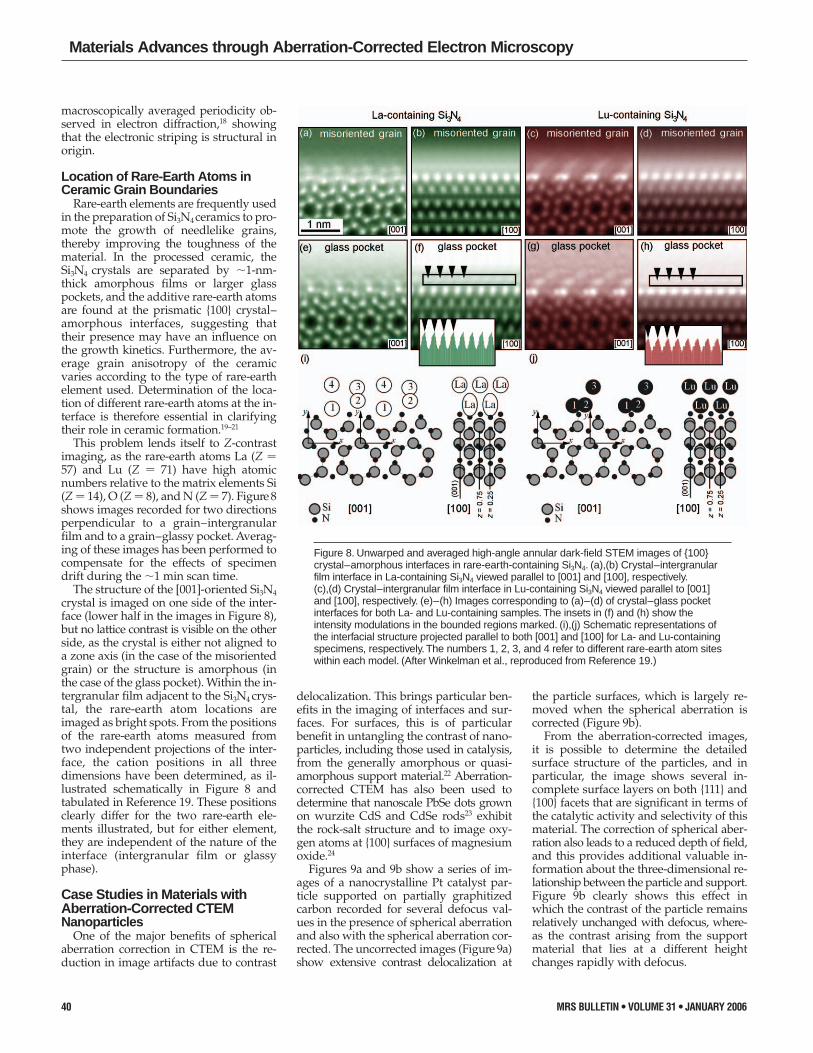
Rare-earth elements are frequently usedin the preparation of Si3N4 ceramics to pro-mote the growth of needlelike grains,thereby improving the toughness of thematerial. In the processed ceramic, theSi3N4 crystals are separated by �1-nm-thick amorphous films or larger glasspockets, and the additive rare-earth atomsare found at the prismatic {100} crystal–amorphous interfaces, suggesting thattheir presence may have an influence onthe growth kinetics. Furthermore, the av-erage grain anisotropy of the ceramicvaries according to the type of rare-earthelement used. Determination of the loca-tion of different rare-earth atoms at the in-terface is therefore essential in clarifyingtheir role in ceramic formation.19–21
This problem lends itself to Z-contrastimaging, as the rare-earth atoms La (Z �57) and Lu (Z � 71) have high atomicnumbers relative to the matrix elements Si(Z � 14), O (Z � 8), and N (Z � 7). Figure 8shows images recorded for two directionsperpendicular to a grain–intergranularfilm and to a grain–glassy pocket. Averag-ing of these images has been performed tocompensate for the effects of specimendrift during the �1 min scan time.
The structure of the [001]-oriented Si3N4crystal is imaged on one side of the inter-face (lower half in the images in Figure 8),but no lattice contrast is visible on the otherside, as the crystal is either not aligned toa zone axis (in the case of the misorientedgrain) or the structure is amorphous (inthe case of the glass pocket). Within the in-tergranular film adjacent to the Si3N4 crys-tal, the rare-earth atom locations areimaged as bright spots. From the positionsof the rare-earth atoms measured fromtwo independent projections of the inter-face, the cation positions in all three dimensions have been determined, as il-lustrated schematically in Figure 8 andtabulated in Reference 19. These positionsclearly differ for the two rare-earth ele-ments illustrated, but for either element,they are independent of the nature of theinterface (intergranular film or glassyphase).
Case Studies in Materials withAberration-Corrected CTEMNanoparticles
One of the major benefits of sphericalaberration correction in CTEM is the re-duction in image artifacts due to contrast
delocalization. This brings particular ben-efits in the imaging of interfaces and sur-faces. For surfaces, this is of particularbenefit in untangling the contrast of nano-particles, including those used in catalysis,from the generally amorphous or quasi-amorphous support material.22 Aberration-corrected CTEM has also been used todetermine that nanoscale PbSe dots grownon wurzite CdS and CdSe rods23 exhibitthe rock-salt structure and to image oxy-gen atoms at {100} surfaces of magnesiumoxide.24
Figures 9a and 9b show a series of im-ages of a nanocrystalline Pt catalyst par-ticle supported on partially graphitizedcarbon recorded for several defocus val-ues in the presence of spherical aberrationand also with the spherical aberration cor-rected. The uncorrected images (Figure 9a)show extensive contrast delocalization at
the particle surfaces, which is largely re-moved when the spherical aberration iscorrected (Figure 9b).
From the aberration-corrected images,it is possible to determine the detailed surface structure of the particles, and inparticular, the image shows several in-complete surface layers on both {111} and{100} facets that are significant in terms ofthe catalytic activity and selectivity of thismaterial. The correction of spherical aber-ration also leads to a reduced depth of field,and this provides additional valuable in-formation about the three-dimensional re-lationship between the particle and support.Figure 9b clearly shows this effect inwhich the contrast of the particle remainsrelatively unchanged with defocus, where-as the contrast arising from the supportmaterial that lies at a different heightchanges rapidly with defocus.
Figure 8. Unwarped and averaged high-angle annular dark-field STEM images of {100}crystal–amorphous interfaces in rare-earth-containing Si3N4. (a),(b) Crystal–intergranularfilm interface in La-containing Si3N4 viewed parallel to [001] and [100], respectively.(c),(d) Crystal–intergranular film interface in Lu-containing Si3N4 viewed parallel to [001]and [100], respectively. (e)–(h) Images corresponding to (a)–(d) of crystal–glass pocketinterfaces for both La- and Lu-containing samples.The insets in (f) and (h) show theintensity modulations in the bounded regions marked. (i),(j) Schematic representations ofthe interfacial structure projected parallel to both [001] and [100] for La- and Lu-containingspecimens, respectively.The numbers 1, 2, 3, and 4 refer to different rare-earth atom siteswithin each model. (After Winkelman et al., reproduced from Reference 19.)
Materials Advances through Aberration-Corrected Electron Microscopy
MRS BULLETIN • VOLUME 31 • JANUARY 2006 41
Defects in SemiconductorsSemiconductors have been extensively
studied by high-resolution CTEM from itsearliest days, and aberration correctionnow enables the direct imaging of indi-vidual atomic columns in several projec-tions at intermediate voltages whereradiation damage is less important. Thishas enabled characterization, at the atomiclevel, of many defects. Preliminary workon SiO2/Si(100) interfaces shows that theelimination of image delocalization offersparticular advantages, and prospects forimaging oxygen atoms at these interfaceshave been explored.25
Stacking faults in Si1–xGex have alsobeen examined by aberration-correctedCTEM and compared with Z-contrast im-ages taken by STEM.26 This work makesthe important point that, even when themicroscope aberrations are corrected, thequality of the specimen is still crucial: inthis case, the presence of a stacking faultleads to localized tilting of the latticearound the fault away from the zone axis.
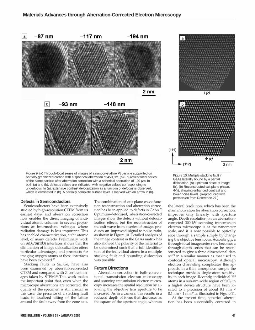
The combination of exit-plane wave func-tion reconstruction and aberration correc-tion has been applied to defects in GaAs.27
Optimum-defocused, aberration-correctedimages show the defects without delocal-ization effects, but the reconstruction ofthe exit wave from a series of images pro-duces an improved signal-to-noise ratio,as shown in Figure 10. Detailed analysis ofthe image contrast in the GaAs matrix hasalso allowed the polarity of the material tobe determined such that a full identifica-tion of the individual atoms in a multiplestacking fault and bounding dislocationwas possible.
Future DirectionsAberration correction in both conven-
tional transmission electron microscopyand scanning transmission electron micros-copy increases the spatial resolution by al-lowing the objective lens aperture to beincreased. As in a camera, this results in areduced depth of focus that decreases asthe square of the aperture angle, whereas
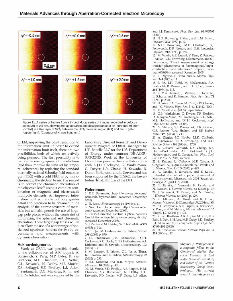
the lateral resolution, which has been themain motivation for aberration correction,improves only linearly with apertureangle. Depth resolution on an aberration-corrected 300-kV scanning transmissionelectron microscope is at the nanometerscale, and it is now possible to opticallyslice through a sample simply by chang-ing the objective lens focus. Accordingly, athrough-focal image series now becomes athrough-depth series that can be recon-structed to give a three-dimensional dataset28 in a similar manner as that used inconfocal optical microscopy. Althoughelectron channeling complicates this ap-proach, in a thin, amorphous sample thetechnique provides single-atom sensitiv-ity in each image. Recently, individual Hfatoms in a sub-nm-wide region of SiO2 ina high-κ device structure have been lo-cated to a precision of about 0.1 nm ×0.1 nm × 1 nm,29 as illustrated in Figure 11.
At the present time, spherical aberra-tion has been successfully corrected in
Figure 9. (a) Through-focal series of images of a nanocrystalline Pt particle supported onpartially graphitized carbon with a spherical aberration of 450 µm. (b) Equivalent focal seriesof the same particle after aberration correction with a spherical aberration of –20 µm. Inboth (a) and (b), defocus values are indicated, with negative values corresponding tounderfocus. In (a), extensive contrast delocalization as a function of defocus is observed,which is eliminated in (b). A partially complete surface layer is marked with an arrow in (b).
Figure 10. Multiple stacking fault inGaAs laterally bound by a partialdislocation. (a) Optimum defocus image,I(r). (b) Reconstructed exit plane phase,Φ(r), showing enhanced contrast andlower noise levels. (Reproduced withpermission from Reference 27.)
42 MRS BULLETIN • VOLUME 31 • JANUARY 2006
Materials Advances through Aberration-Corrected Electron Microscopy
CTEM, improving the point resolution tothe information limit. In order to extendthe information limit itself, there are twopossibilities, both of which are activelybeing pursued. The first possibility is toreduce the energy spread of the electrons(and thus improve the limit set by tempo-ral coherence) by replacing the standardthermally assisted Schottky field-emissiongun (FEG) with a cold FEG, or by mono-chromating the electron beam. The secondis to correct the chromatic aberration ofthe objective lens30 using a complex com-bination of magnetic and electrostaticmultipole elements. An improved infor-mation limit will allow not only greaterdetail and precision to be obtained in theanalysis of the atomic structure of mate-rials but will also permit the use of large-gap pole pieces without the constraint ofminimizing the spherical and chromaticaberration. These larger gap lenses will inturn allow the use of a wider range of spe-cialized specimen holders for in situ ex-periments and measurements withdynamic observation.
AcknowledgmentsWork at ORNL was possible thanks
to the collaboration of A.R. Lupini, A.Borisevich, Y. Peng, M.P. Oxley, K. vanBenthem, M.F. Chisholm, P.D. Nellist, O.L. Krivanek, N. Dellby, M.F. Murfitt,Z.S. Szilagyi, S.F. Findlay, L.J. Allen, J. Santamaria, D.G. Mandrus, R. Jin, andS.T. Pantelides, and was supported by the
Laboratory Directed Research and Devel-opment Program of ORNL, managed byUT–Battelle LLC for the U.S. Departmentof Energy under contract DE-AC05–000R22725. Work at the University of Oxford was possible due to collaborationswith D.J.H. Cockayne, G. Winkelmann, C. Dwyer, L.Y. Chang, H. Sawada, R.Dunin-Borkowski, and L. Cervera and hasbeen supported by the EPSRC, the Lever-hulme Trust, JEOL, and the DTI.
References1. R.P. Feynman, http://www.zyvex.com/nanotech/feynman.html (accessed December2005).2. H. Rose, Ultramicroscopy 56 (1994) p. 11.3. Nion Co. Home Page, http://www.nion.com/ (accessed December 2005).4. CEOS–Corrected Electron Optical SystemsGmbH Home Page, http://www.ceos-gmbh.de/(accessed December 2005).5. J. Zach and M. Haider, Nucl. Inst. Meth. A363(1995) p. 316.6. C.L. Jia, M. Lentzen, and K. Urban, Science299 (2003) p. 870.7. J.L. Hutchison, J.M. Titchmarsh, D.J.H. Cockayne, R.C. Doole, C.J.D. Hetherington, A.I.Kirkland, and H. Sawada, Ultramicroscopy 103(2005) p. 7.8. M. Lentzen, B. Jahnen, C.L. Jia, A. Thust, K. Tillmann, and K. Urban, Ultramicroscopy 92(2002) p. 233.9. A.I. Kirkland and R.R. Meyer, Microsc. Microanal. 10 (2004) p. 401.10. M. Varela, S.D. Findlay, A.R. Lupini, H.M.Christen, A.Y. Borisevich, N. Dellby, O.L. Krivanek, P.D. Nellist, M.P. Oxley, L.J. Allen,
and S.J. Pennycook, Phys. Rev. Lett. 92 095502(2004).11. N.D. Browning, J. Yuan, and L.M. Brown,Physica C 202 (1992) p. 12.12. N.D. Browning, M.F. Chisholm, S.J. Pennycook, D.P. Norton, and D.H. Lowndes,Physica C 212 (1993) p. 185.13. M. Varela, A.R. Lupini, V. Pena, Z. Sefrioui,I. Arslan, N.D. Browning, J. Santamaria, and S.J.Pennycook, “Direct measurement of chargetransfer phenomena at ferromagnetic/super-conducting oxide interfaces,” preprint, cond-mat/0508564 (accessed December 2005).14. E. Dagotto, T. Hotta, and A. Moreo, Phys.Rep. 344 (2001) p. 1.15. S. Jin, T.H. Tiefel, M. McCormack, R.A. Fastnacht, R. Ramesh, and L.H. Chen, Science264 (1994) p. 413.16. R. Von Helmolt, J. Wecker, B. Holzapfel, L. Schultz, and K. Samwer, Phys. Rev. Lett. 71(1993) p. 2331.17. H. Woo, T.A. Tyson, M. Croft, S.W. Cheong,and J.C. Woicik, Phys. Rev. B 63 134412 (2001).18. M. Varela et al. (2005) unpublished. 19. G.B. Winkelman, C. Dwyer, T.S. Hudson, D. Nguyen-Manh, M. Doeblinger, R.L. Satet,M.J. Hoffmann, and D.J.H. Cockayne, Appl.Phys. Lett. 87 061911 (2005).20. N. Shibata, S.J. Pennycook, T.R. Gosnell,G.S. Painter, W.A. Shelton, and P.F. Becher, Nature 428 (2004) p. 730.21. A. Ziegler, J.C. Idrobo, M.K. Cinibulk, C. Kisielowski, N.D. Browning, and R.O.Ritchie, Science 306 (2004) p. 1768.22. L. Cervera Gontard, L-Y Chang, R.E.Dunin-Borkowski, A.I. Kirkland, C.J.D. Hetherington, and D. Ozkaya, Inst. Phys. Conf.Ser. EMAG 05 (2005) in press.23. S. Kudera, L. Carbone, M.F. Casula, R. Cingolani, A. Falqui, E. Snoeck, W.J. Parak, andL. Manna, Nano Lett. 5 (2005) p. 445.24. N. Tanaka, J. Yamasaki, and T. Kawai, Extended abstract of a paper presented at Microscopy and Microanalysis 2004 (Savannah,Georgia, August 1–5, 2004).25. N. Tanaka, J. Yamasaki, K. Usuda, and N. Ikarashi, J. Electron Microsc. 52 (2003) p. 69.26. J. Yamasaki, T. Kawai, and N. Tanaka,J. Electron Microsc. 53 (2004) p. 129.27. K. Tillmann, A. Thust, and K. Urban, Microsc. Microanal. 10 (Cambridge UP, 2004) p. 185.28. S.J. Pennycook, A.R. Lupini, A. Borisevich,Y. Peng, and N. Shibata, Microsc. Microanal. 10(Suppl. 1.2) (2004) p. 1172.29. K. van Benthem, A.R. Lupini, M. Kim, H.S.Baik, S. Doh, J.-H. Lee, M.P. Oxley, S.D. Findlay,L.J. Allen, and S.J. Pennycook, Appl. Phys. Lett.87 034104 (2005).30. H. Rose, Nucl. Instrum. Methods Phys. Res. A519 (2004) p. 12.
Stephen J. Pennycook isa corporate fellow in theCondensed Matter Sci-ences Division at OakRidge National Laboratoryand leader of the ElectronMicroscopy Group (stem.ornl.gov). His current research interests focus on
Figure 11. A series of frames from a through-focal series of images, recorded in defocussteps (∆f) of 0.5 nm, showing the appearance and disappearance of an individual Hf atom(circled) in a thin layer of SiO2 between the HfO2 dielectric region (left) and the Si gateregion (right). (Courtesy of K. van Benthem.)
Materials Advances through Aberration-Corrected Electron Microscopy
MRS BULLETIN • VOLUME 31 • JANUARY 2006 43
the development of Z-contrast scanning trans-mission electron microscopy and electron energyloss spectroscopy with sub-angstrom resolution,and their applications to materials science, catal-ysis, biology, and nanoscience. He is a recipient ofthe Materials Research Society Medal and theThomas Young Medal of the Institute of Physics.
Pennycook can be reached at Oak Ridge Na-tional Laboratory, Condensed Matter SciencesDivision, PO Box 2008, Oak Ridge, TN 37831-6030 USA; tel. 865-574-5504, fax 865-574-4143,and e-mail [email protected].
Maria Varela is an Elec-tron Microscopy Group re-search staff member in theCondensed Matter Sci-ences Division at OakRidge National Labora-tory. She received her PhDdegree in solid-statephysics from the Com-plutense University of
Madrid, Spain. She has wide experience in thegrowth, physical properties, measurements, andstructural characterization of thin films, in par-ticular, high-temperature superconducting thinfilms and superlattices. Her current research in-terests focus on the study of the properties of com-
plex oxide thin films and interfaces by means ofaberration-corrected Z-contrast scanning trans-mission electron microscopy and electron energyloss spectroscopy with sub-angstrom resolution.She has authored over 60 papers in journals suchas the Journal of Materials Research, PhysicalReview Letters, and Nature. She is also a recip-ient of the Royal Spanish Physics Society Awardfor Novel Researchers and the Oak Ridge Na-tional Laboratory Wigner Fellowship.
Varela can be reached at Condensed MatterSciences Division, Oak Ridge National Labora-tory, PO Box 2008, Bldg. 3025M, MS 6031, OakRidge, TN 37831-6031 USA; tel. 865-574 6287,fax 865-574 4143, and e-mail [email protected].
Crispin J.D. Hetheringtonis a research fellow in theDepartment of Materialsat Oxford University,where he also earned hisundergraduate and DPhildegrees. He has worked ina number of electronmicroscopy facilities, in-cluding the National Cen-
ter for Electron Microscopy in Berkeley, Calif.,and Sheffield and Cambridge in the United King-dom. His research interests are the characteriza-
tion of interfaces and materials at the atomic levelthrough the use of aberration-corrected microscopy.
Hetherington can be reached at University ofOxford, Department of Materials, Parks Rd., Ox-ford OX1 3PH, United Kingdom; tel. 44-1865-283740, fax 44-1865-848790, and [email protected].
Angus I. Kirkland hasbeen a professor of mate-rials at the University ofOxford since 2005. He wasawarded his MA and PhDdegrees from the Univer-sity of Cambridge. His cur-rent research interestsinclude applications ofaberration-corrected high-
resolution transmission electron microscopy forstructural studies of nanomaterials, the design ofdirect electron detectors, and the development ofcomputational image processing and theory forenhancing resolution in TEM. He is a fellow ofthe Institute of Physics and of the Royal Societyof Chemistry.
Kirkland can be reached at the University ofOxford, Department of Materials, Parks Rd., Oxford OX1 3PH, United Kingdom; [email protected].
For more information, see http://advertisers.mrs.org
www.mrs.org/publications/bulletin