Embed Size (px)
Citation preview
Aberration-corrected TEM studies on interface of multilayered-perovskite systems
ByLina Gunawan (0326114)
Supervisor: Dr. Gianluigi BottonNovember 1, 2006
MSE 702(1) Presentation
Nov 1, 2006McMaster Univ. - MSE 702(1) Presentation2
Outline
� Literature Review� Perovskite double-oxides � Issues of interface in thin films� TEM Features & Role of CS-corrector
� Objectives� Characterization across interface
• experimental & simulation
� Assessment • physical properties changes ⇔ structural changes
� Experimental Techniques
Nov 1, 2006McMaster Univ. - MSE 702(1) Presentation3
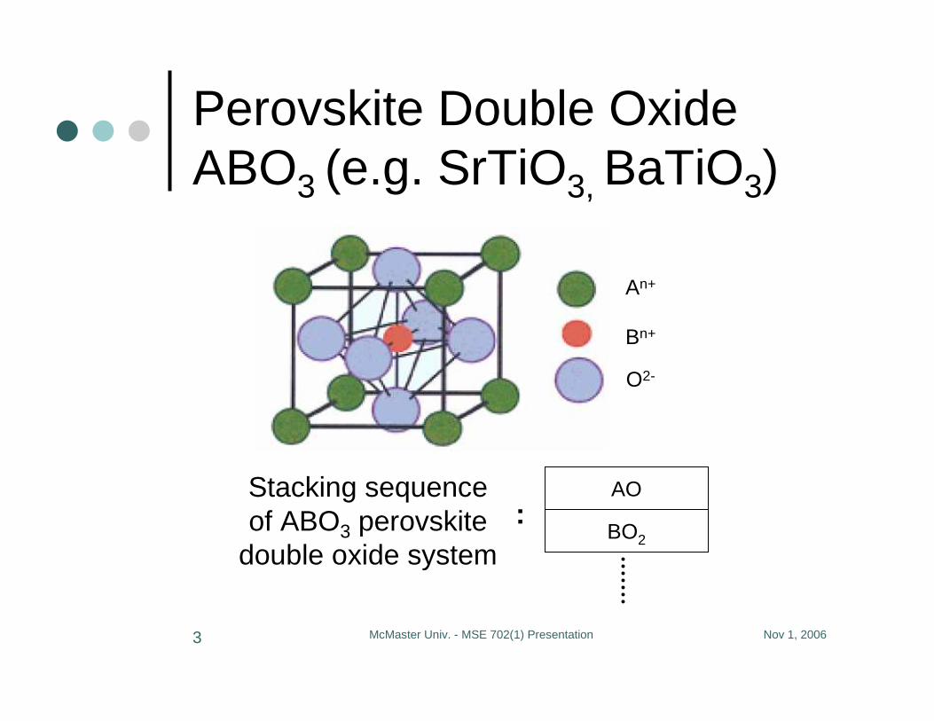
Perovskite Double Oxide ABO3 (e.g. SrTiO3, BaTiO3)
An+
O2-
Bn+
AO
BO2
Stacking sequence of ABO3 perovskite
double oxide system:
Nov 1, 2006McMaster Univ. - MSE 702(1) Presentation4
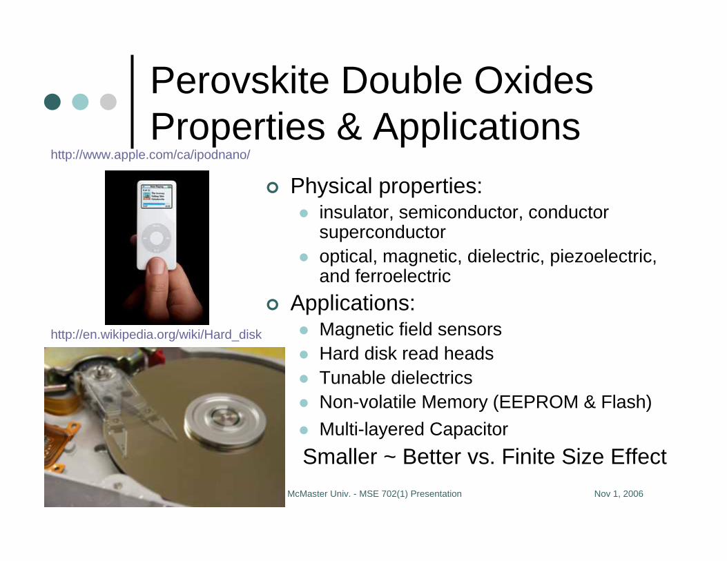
Perovskite Double OxidesProperties & Applications
� Physical properties:� insulator, semiconductor, conductor
superconductor� optical, magnetic, dielectric, piezoelectric,
and ferroelectric
� Applications:� Magnetic field sensors� Hard disk read heads� Tunable dielectrics� Non-volatile Memory (EEPROM & Flash)
� Multi-layered Capacitor
� Smaller ~ Better vs. Finite Size Effect
http://www.apple.com/ca/ipodnano/
http://en.wikipedia.org/wiki/Hard_disk
Nov 1, 2006McMaster Univ. - MSE 702(1) Presentation5
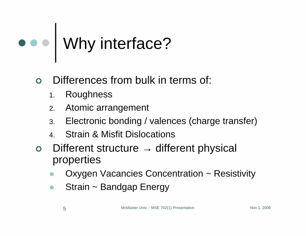
Why interface?
� Differences from bulk in terms of:1. Roughness2. Atomic arrangement3. Electronic bonding / valences (charge transfer)4. Strain & Misfit Dislocations
� Different structure → different physical properties� Oxygen Vacancies Concentration ~ Resistivity� Strain ~ Bandgap Energy
Nov 1, 2006McMaster Univ. - MSE 702(1) Presentation6
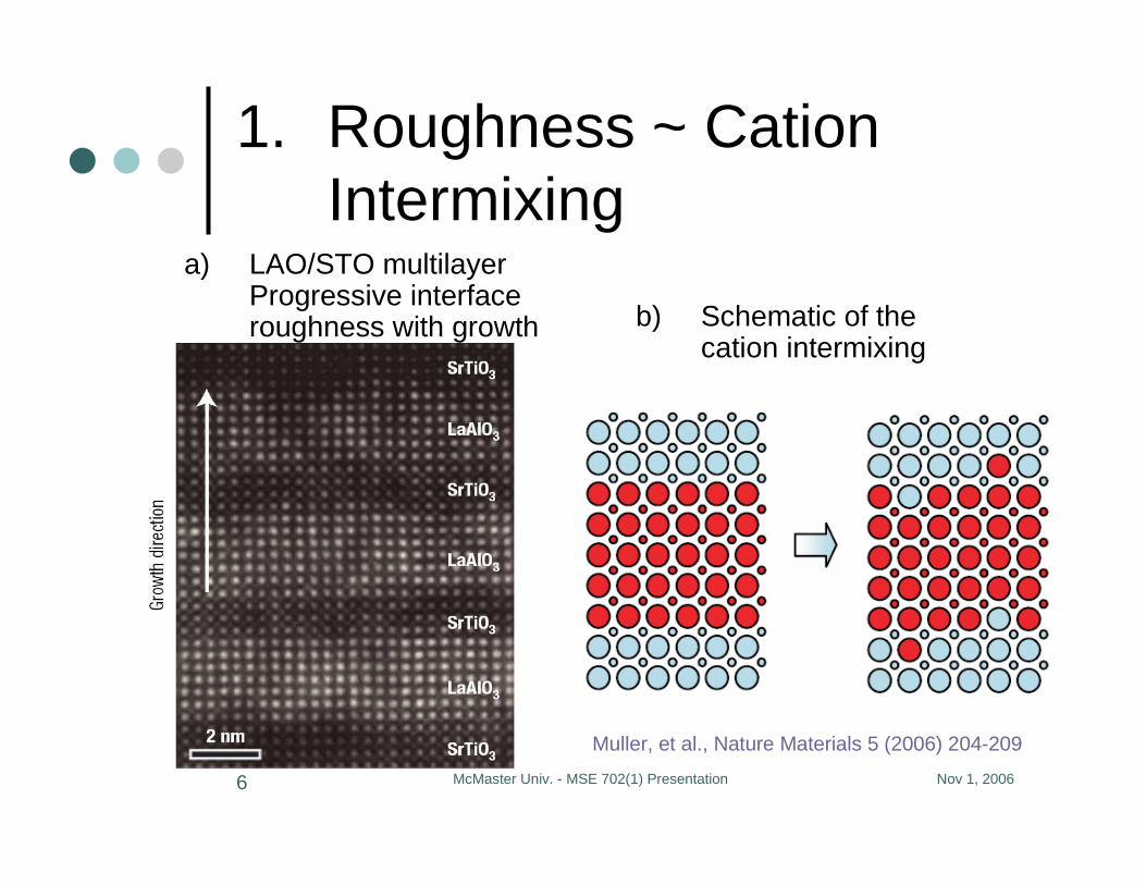
1. Roughness ~ CationIntermixing
b) Schematic of the cation intermixing
Muller, et al., Nature Materials 5 (2006) 204-209
a) LAO/STO multilayerProgressive interface roughness with growth
Nov 1, 2006McMaster Univ. - MSE 702(1) Presentation7
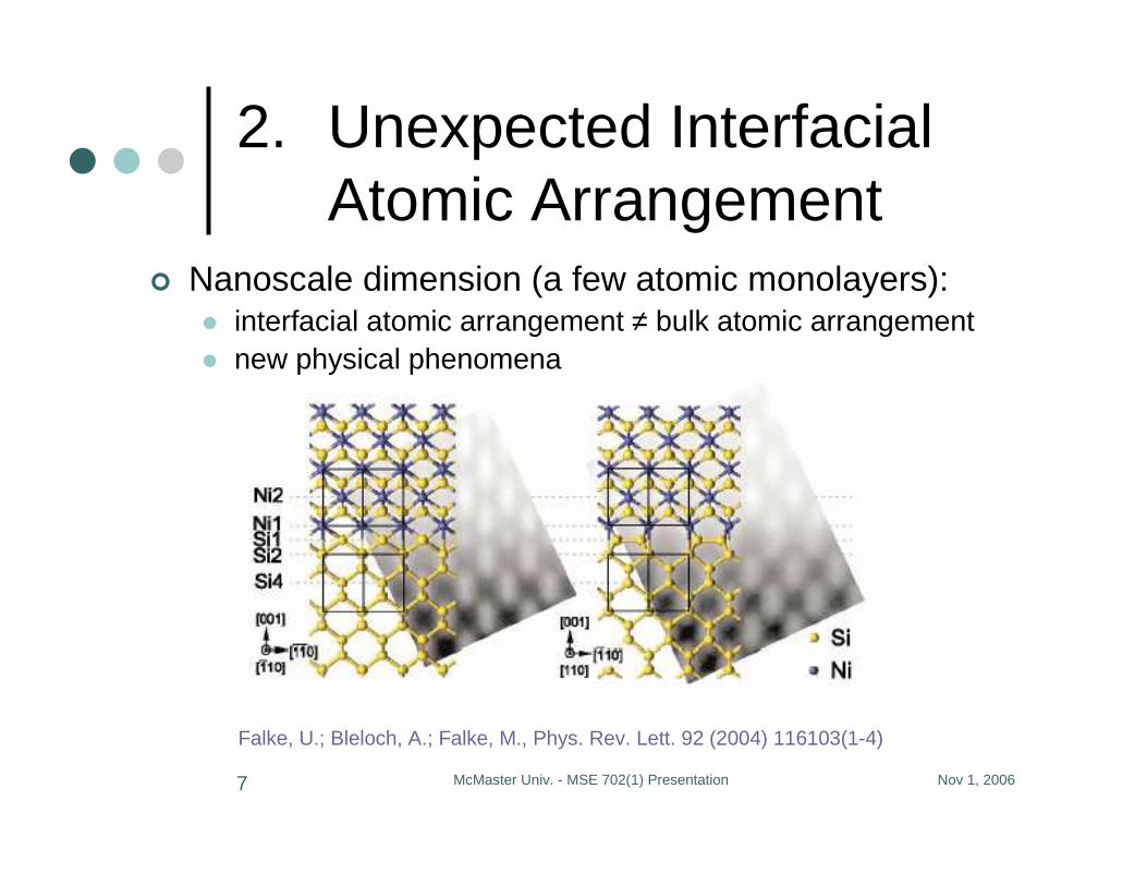
2. Unexpected Interfacial Atomic Arrangement
� Nanoscale dimension (a few atomic monolayers):� interfacial atomic arrangement ≠ bulk atomic arrangement � new physical phenomena
Falke, U.; Bleloch, A.; Falke, M., Phys. Rev. Lett. 92 (2004) 116103(1-4)
Nov 1, 2006McMaster Univ. - MSE 702(1) Presentation8
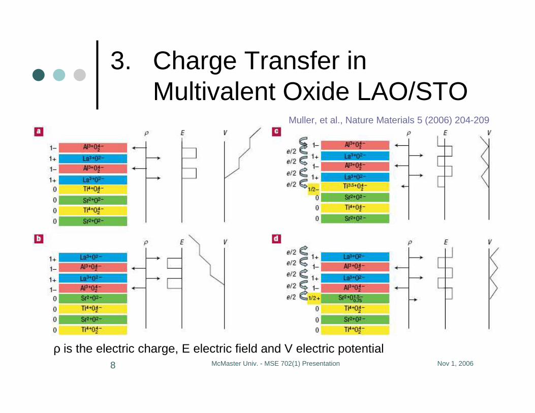
3. Charge Transfer inMultivalent Oxide LAO/STO
Muller, et al., Nature Materials 5 (2006) 204-209
ρ is the electric charge, E electric field and V electric potential
Nov 1, 2006McMaster Univ. - MSE 702(1) Presentation9
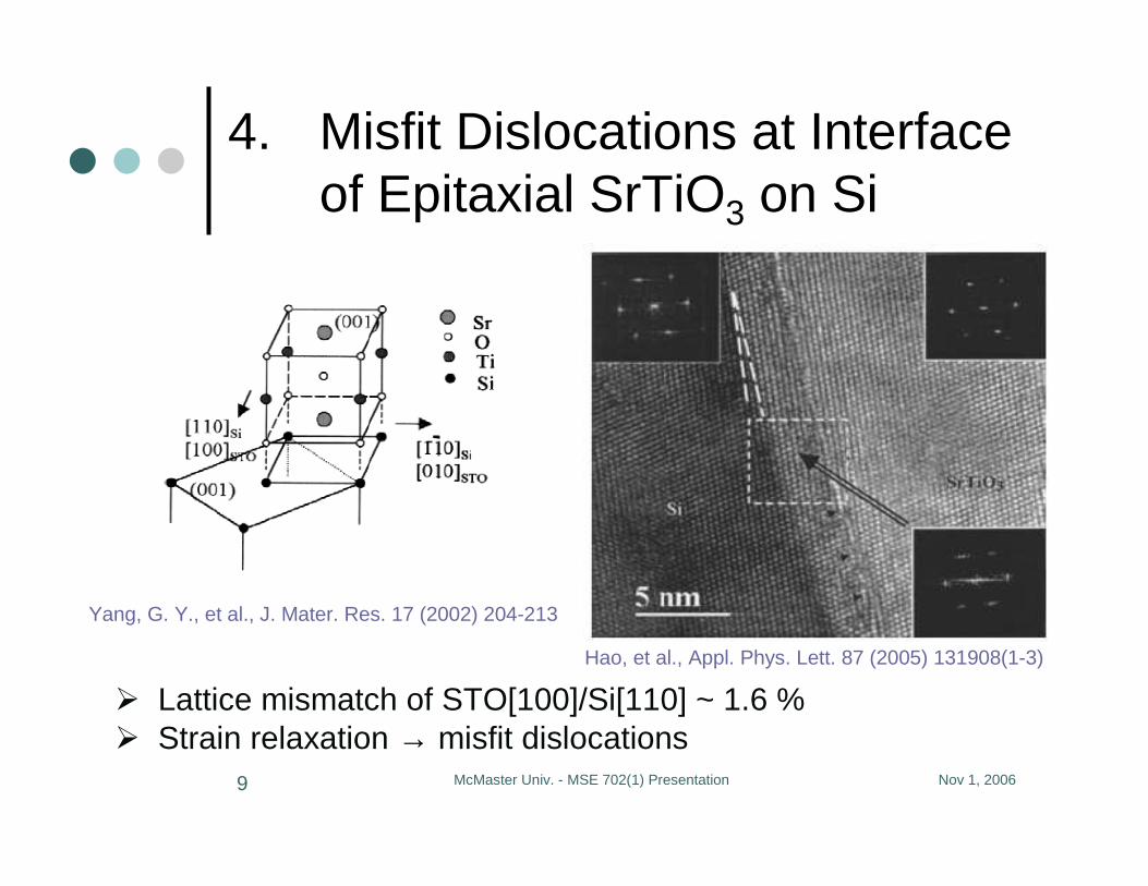
4. Misfit Dislocations at Interface of Epitaxial SrTiO3 on Si
Yang, G. Y., et al., J. Mater. Res. 17 (2002) 204-213
� Lattice mismatch of STO[100]/Si[110] ~ 1.6 % � Strain relaxation → misfit dislocations
Hao, et al., Appl. Phys. Lett. 87 (2005) 131908(1-3)
Nov 1, 2006McMaster Univ. - MSE 702(1) Presentation10
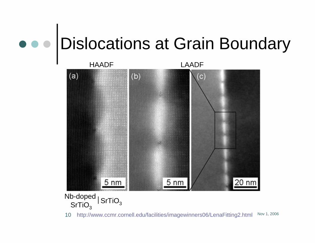
Dislocations at Grain BoundaryHAADF
SrTiO3Nb-doped
SrTiO3
http://www.ccmr.cornell.edu/facilities/imagewinners06/LenaFitting2.html
LAADF
Nov 1, 2006McMaster Univ. - MSE 702(1) Presentation11
Detailed Investigation at Interface� Many Interesting Phenomena at Interface� New insight into unexpected physical
properties � conductivity = f (VO concentration)
� Ways to control and modify the interface � New generation CS-corrected TEM (sub-Å
probe) � Atomic scale characterization� Qualitative & quantitative information
o HREM and Z-contrast images o EELS spectra
Nov 1, 2006McMaster Univ. - MSE 702(1) Presentation12
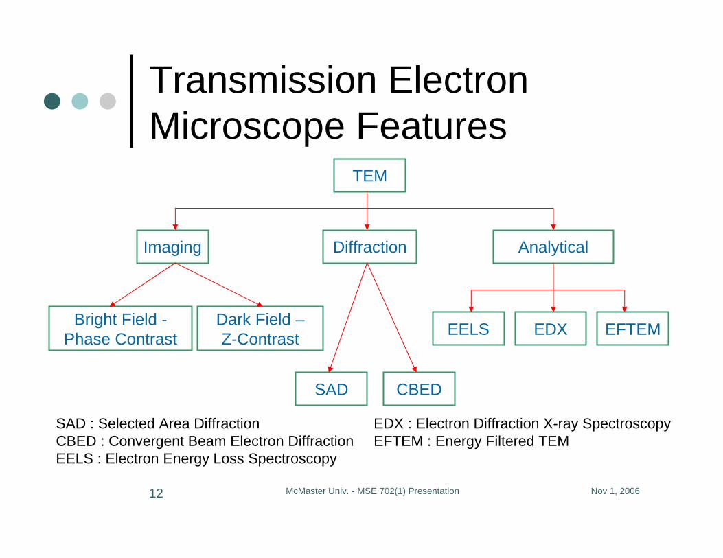
Transmission Electron Microscope Features
EDX
Analytical
EELS EFTEM
TEM
Imaging Diffraction
Dark Field –Z-Contrast
Bright Field -Phase Contrast
SAD CBED
SAD : Selected Area DiffractionCBED : Convergent Beam Electron DiffractionEELS : Electron Energy Loss Spectroscopy
EDX : Electron Diffraction X-ray SpectroscopyEFTEM : Energy Filtered TEM
Nov 1, 2006McMaster Univ. - MSE 702(1) Presentation13
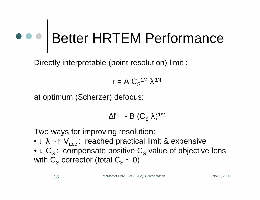
Better HRTEM Performance
Directly interpretable (point resolution) limit :
r = A CS1/4 λ3/4
at optimum (Scherzer) defocus:
∆f = - B (CS λ)1/2
Two ways for improving resolution:• ↓ λ ~↑ Vacc : reached practical limit & expensive• ↓ CS : compensate positive CS value of objective lens with CS corrector (total CS ~ 0)
Nov 1, 2006McMaster Univ. - MSE 702(1) Presentation14
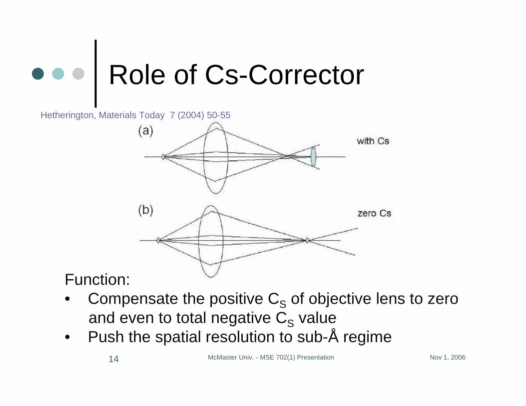
Role of Cs-CorrectorHetherington, Materials Today 7 (2004) 50-55
Function:• Compensate the positive CS of objective lens to zero
and even to total negative CS value• Push the spatial resolution to sub-Å regime
Nov 1, 2006McMaster Univ. - MSE 702(1) Presentation15
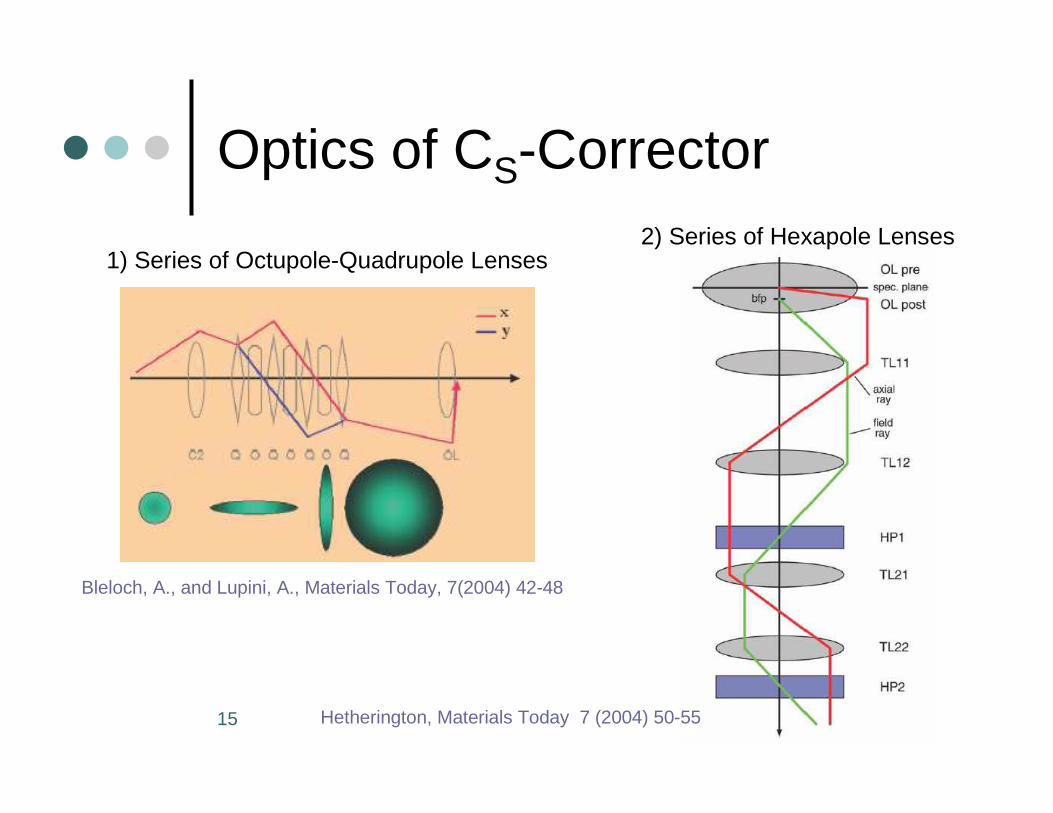
Optics of CS-Corrector
Bleloch, A., and Lupini, A., Materials Today, 7(2004) 42-48
Hetherington, Materials Today 7 (2004) 50-55
1) Series of Octupole-Quadrupole Lenses2) Series of Hexapole Lenses
Nov 1, 2006McMaster Univ. - MSE 702(1) Presentation16
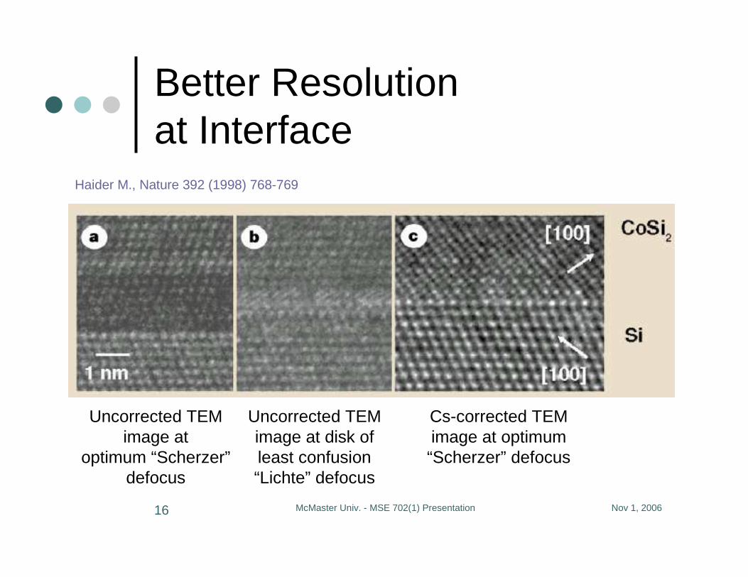
Better Resolution at Interface
Haider M., Nature 392 (1998) 768-769
Uncorrected TEM image at
optimum “Scherzer”defocus
Uncorrected TEM image at disk of least confusion “Lichte” defocus
Cs-corrected TEM image at optimum“Scherzer” defocus
Nov 1, 2006McMaster Univ. - MSE 702(1) Presentation17
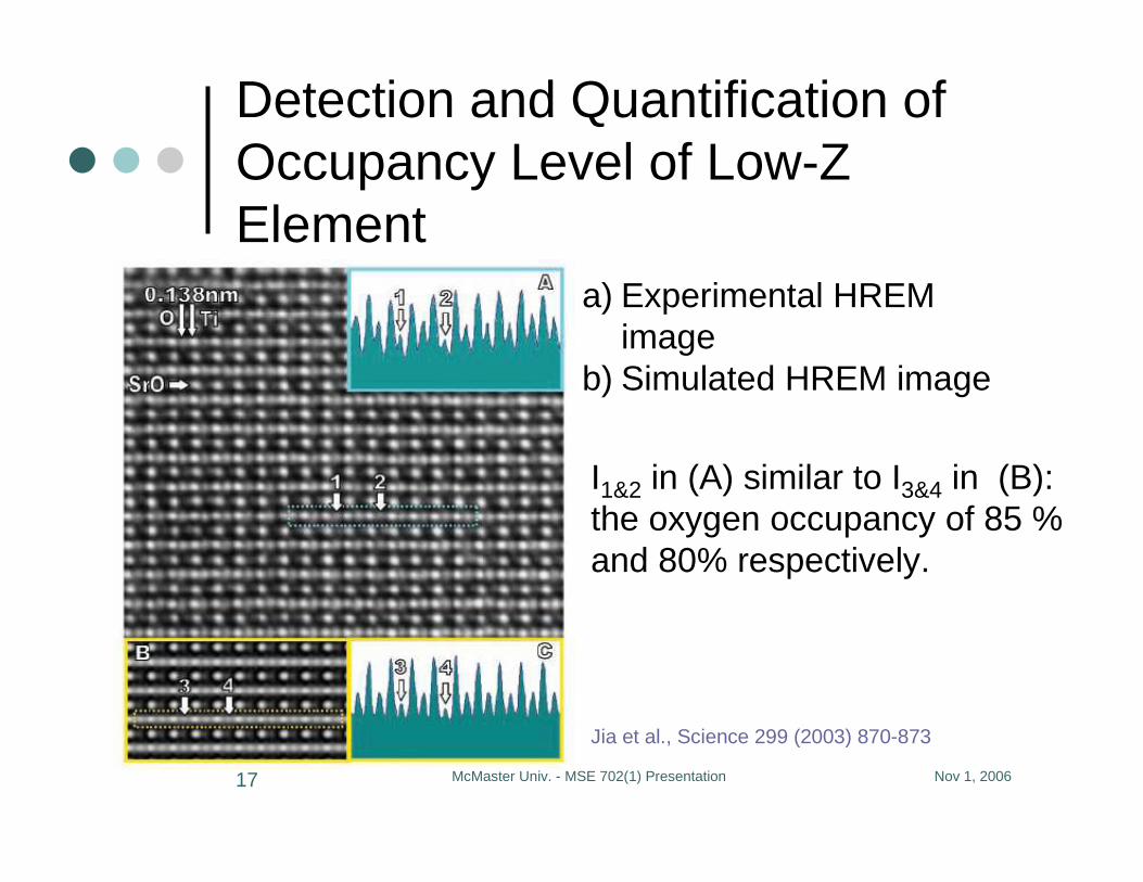
Detection and Quantification of Occupancy Level of Low-Z Element
a) Experimental HREM image
b) Simulated HREM image
Jia et al., Science 299 (2003) 870-873
I1&2 in (A) similar to I3&4 in (B): the oxygen occupancy of 85 % and 80% respectively.
Nov 1, 2006McMaster Univ. - MSE 702(1) Presentation18
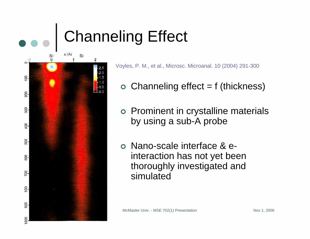
Channeling Effect
� Channeling effect = f (thickness)
� Prominent in crystalline materials by using a sub-A probe
� Nano-scale interface & e-interaction has not yet been thoroughly investigated and simulated
Voyles, P. M., et al., Microsc. Microanal. 10 (2004) 291-300
Nov 1, 2006McMaster Univ. - MSE 702(1) Presentation19
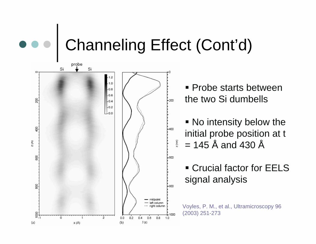
Channeling Effect (Cont’d)
Voyles, P. M., et al., Ultramicroscopy 96 (2003) 251-273
� Probe starts between the two Si dumbells
� No intensity below the initial probe position at t= 145 Å and 430 Å
� Crucial factor for EELS signal analysis
Nov 1, 2006McMaster Univ. - MSE 702(1) Presentation20
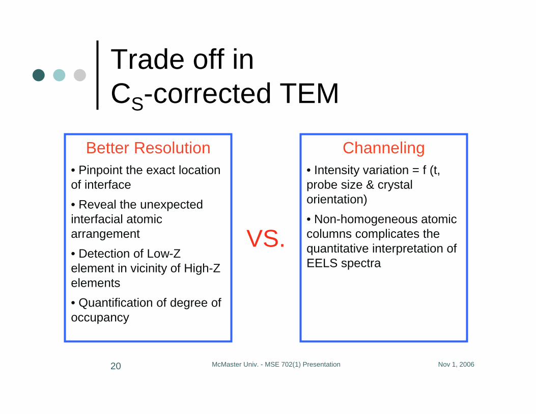
Trade off in CS-corrected TEM
Better Resolution• Pinpoint the exact location of interface
• Reveal the unexpected interfacial atomic arrangement
• Detection of Low-Z element in vicinity of High-Z elements
• Quantification of degree of occupancy
Channeling• Intensity variation = f (t, probe size & crystal orientation)
• Non-homogeneous atomic columns complicates the quantitative interpretation of EELS spectra
VS.
Nov 1, 2006McMaster Univ. - MSE 702(1) Presentation21
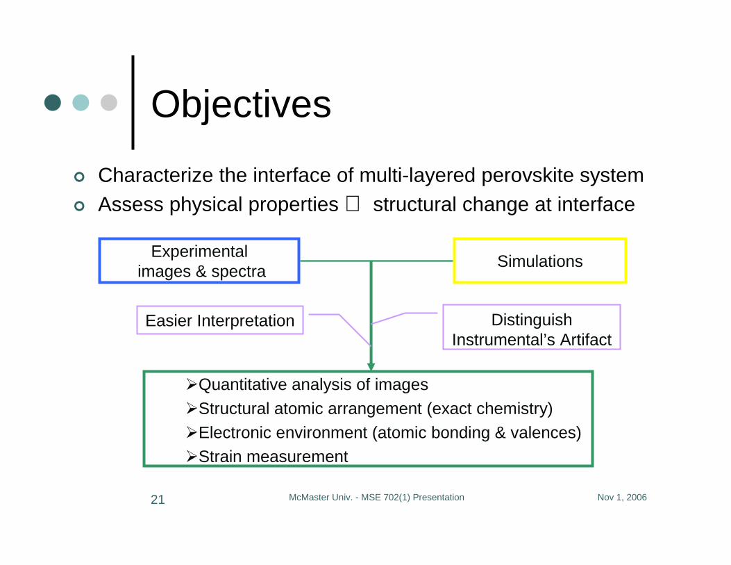
Objectives
� Characterize the interface of multi-layered perovskite system� Assess physical properties ⇔ structural change at interface
Experimentalimages & spectra
Simulations
�Quantitative analysis of images
�Structural atomic arrangement (exact chemistry)
�Electronic environment (atomic bonding & valences)�Strain measurement
Distinguish Instrumental’s Artifact
Easier Interpretation
Nov 1, 2006McMaster Univ. - MSE 702(1) Presentation22
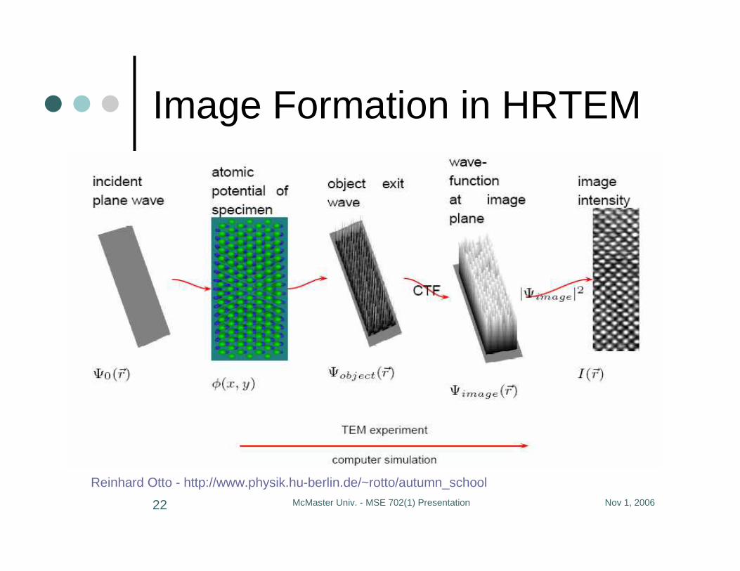
Image Formation in HRTEM
Reinhard Otto - http://www.physik.hu-berlin.de/~rotto/autumn_school
Nov 1, 2006McMaster Univ. - MSE 702(1) Presentation23
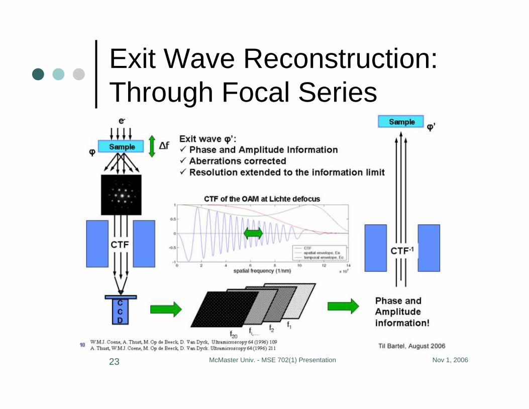
Exit Wave Reconstruction:Through Focal Series
Nov 1, 2006McMaster Univ. - MSE 702(1) Presentation24
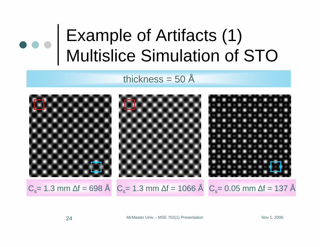
Example of Artifacts (1)Multislice Simulation of STO
Cs= 1.3 mm ∆f = 698 Å Cs= 1.3 mm ∆f = 1066 Å Cs= 0.05 mm ∆f = 137 Å
thickness = 50 Å
Nov 1, 2006McMaster Univ. - MSE 702(1) Presentation25
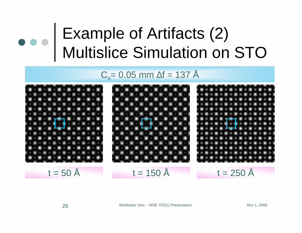
Example of Artifacts (2)Multislice Simulation on STO
Cs= 0.05 mm ∆f = 137 Å
t = 50 Å t = 150 Å t = 250 Å
Nov 1, 2006McMaster Univ. - MSE 702(1) Presentation26
Experimental Techniques� Conventional and Cs-Corrected HRTEM
� Image (BF or HAADF) – sub-Å resolution: » the atomic arrangement, strain measurement
� SAD: » unit cell structure and phase
� EDX: » chemical composition
� EELS: » electronic environment: oxidation state, atomic valences, and interatomic bondings
� CBED: » strain measurement & lattice parameter determination at interface
Nov 1, 2006McMaster Univ. - MSE 702(1) Presentation27
Potential Perovskite Systems for Multilayer Integration
• LaAlO3/(Sr,La)O3
• SrRuO3/cuprate
• (La,Ca)CuO3/cuprate
• Cuprate/manganate
• SrTiO3/LaMnO3/La(Al, Sc)O3
• LaAlO3/SrTiO3
Nov 1, 2006McMaster Univ. - MSE 702(1) Presentation28
Future Works
� Experimental TEM & analytical characterization of the interface of multilayered perovskite double oxides.
� Simulations:� Multislice image simulation:
• Distinguishing artifacts from the real materials’ features (e. g. unexpected atomic arrangement)
• Observing e- propagation at interface� Spectrum simulation:
• Analytical interpretation of the interfacial atoms• Valences/chemistry, composition, and bonding
Nov 1, 2006McMaster Univ. - MSE 702(1) Presentation29
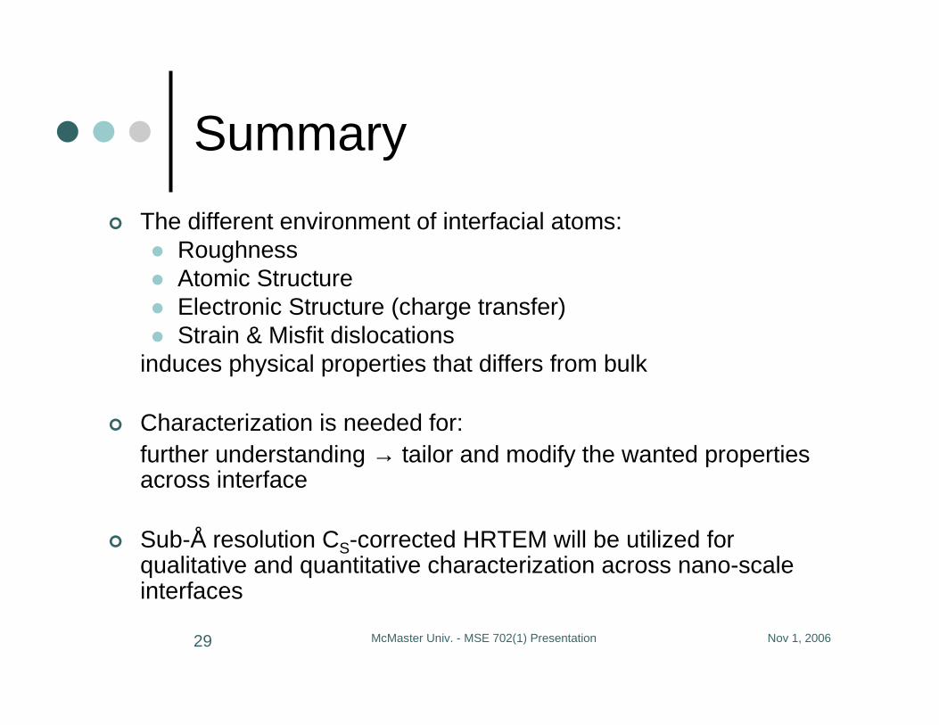
Summary
� The different environment of interfacial atoms: � Roughness � Atomic Structure� Electronic Structure (charge transfer)� Strain & Misfit dislocations
induces physical properties that differs from bulk
� Characterization is needed for:further understanding → tailor and modify the wanted properties across interface
� Sub-Å resolution CS-corrected HRTEM will be utilized for qualitative and quantitative characterization across nano-scale interfaces
Nov 1, 2006McMaster Univ. - MSE 702(1) Presentation30
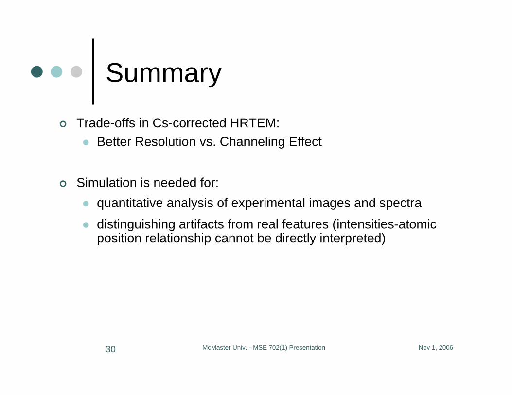
Summary
� Trade-offs in Cs-corrected HRTEM:� Better Resolution vs. Channeling Effect
� Simulation is needed for:
� quantitative analysis of experimental images and spectra
� distinguishing artifacts from real features (intensities-atomic position relationship cannot be directly interpreted)
Nov 1, 2006McMaster Univ. - MSE 702(1) Presentation31
References
� Haider M., Nature 392 (1998) 768-769
� Yang, G. Y., et al., J. Mater. Res. 17 (2002) 204-213
� Voyles, P. M., Grazul, J. L., Muller, D. A., Ultramicroscopy 96 (2003) 251-273
� Hu, et al., Appl. Phys. Lett. 82 (2003) 203-205
� Falke, U.; Bleloch, A.; Falke, M., Phys. Rev. Lett. 92 (2004) 116103(1-4)
� Voyles, P. M., Muller, D. A., Kirkland, E. J., Microsc. Microanal. 10 (2004) 291-300
� Hao, et al., Appl. Phys. Lett. 87 (2005) 131908(1-3)
� Hetherington, Materials Today 7 (2004) 50-55� Muller, et al., Nature Materials 5 (2006) 204-209
� Yu, et al., Thin Solid Films 462-463 (2004) 51-56
� He, et al., J. Appl. Phys. 97 (2005) 104921(1-6)
Nov 1, 2006McMaster Univ. - MSE 702(1) Presentation32
Acknowledgement
� Dr. Gianluigi Botton� Dr. Carmen Andrei� Dr. Christian Maunders� Nadi, Yang & Kai� Fred Pearson� Dr. Maria Varela (Oak Ridge Nat’l Lab)
Thank You
Questions ???


![corrigée des aberrations a révolutionné notre ... · Effect of the aberration corrector on high resolution in TEM imaging. GaAs projected along the [110] zone axis . Non corrected](https://img.pdfslide.net/doc/110x75/5ba8377009d3f23f4e8c2b31/corrigee-des-aberrations-a-revolutionne-notre-effect-of-the-aberration.jpg)