Embed Size (px)
Citation preview
8/4/2019 Analogue-electronics Laboratory Protocol
http://slidepdf.com/reader/full/analogue-electronics-laboratory-protocol 1/43
analogue electronics
protocol for the laboratory work
Matthias Pospiech, Sha Liu
31st January 2004
8/4/2019 Analogue-electronics Laboratory Protocol
http://slidepdf.com/reader/full/analogue-electronics-laboratory-protocol 2/43
Contents
1. Operational Amplifiers 3
2. Circuits with Operational Amplifiers 52.1. Inverting Operational Amplifier . . . . . . . . . . . . . . . . . . . . . . . . . . 52.2. Integrator . . . . . . . . . . . . . . . . . . . . . . . . . . . . . . . . . . . . . . 72.3. Differentiator . . . . . . . . . . . . . . . . . . . . . . . . . . . . . . . . . . . . 92.4. PID servo . . . . . . . . . . . . . . . . . . . . . . . . . . . . . . . . . . . . . . 12
3. Digitizing and spectral analysis 153.1. Fourier transformation (theory) . . . . . . . . . . . . . . . . . . . . . . . . . . 15
3.1.1. Fourier series . . . . . . . . . . . . . . . . . . . . . . . . . . . . . . . . 153.1.2. Fourier transformation . . . . . . . . . . . . . . . . . . . . . . . . . . . 16
3.1.3. discrete Fourier transformation . . . . . . . . . . . . . . . . . . . . . . 163.1.4. fast Fourier transformation . . . . . . . . . . . . . . . . . . . . . . . . 17
3.2. Sampling rates / sampling theorem . . . . . . . . . . . . . . . . . . . . . . . . 173.2.1. Nyquist Frequency . . . . . . . . . . . . . . . . . . . . . . . . . . . . . 173.2.2. Sampling theorem . . . . . . . . . . . . . . . . . . . . . . . . . . . . . 18
3.3. Aliasing . . . . . . . . . . . . . . . . . . . . . . . . . . . . . . . . . . . . . . . 193.4. Spectral analysis of sine, rectangular and triangular signals . . . . . . . . . . 21
3.4.1. sine . . . . . . . . . . . . . . . . . . . . . . . . . . . . . . . . . . . . . 213.4.2. rectangular . . . . . . . . . . . . . . . . . . . . . . . . . . . . . . . . . 213.4.3. triangular . . . . . . . . . . . . . . . . . . . . . . . . . . . . . . . . . . 22
3.5. Overloading of the Op-amplifiers . . . . . . . . . . . . . . . . . . . . . . . . . 24
4. Modulation 254.1. Frequency modulation (FM) . . . . . . . . . . . . . . . . . . . . . . . . . . . . 254.2. Amplitude modulation (AM) . . . . . . . . . . . . . . . . . . . . . . . . . . . 274.3. Comparison of both modulation techniques . . . . . . . . . . . . . . . . . . . 29
5. Noise 305.1. Different noise processes . . . . . . . . . . . . . . . . . . . . . . . . . . . . . . 305.2. Spectral properties of the noise generator . . . . . . . . . . . . . . . . . . . . 335.3. Methods to improve the signal to noise ratio . . . . . . . . . . . . . . . . . . . 335.4. Correlation of noise . . . . . . . . . . . . . . . . . . . . . . . . . . . . . . . . . 35
A. measuring data 37A.1. Operational Amplifiers . . . . . . . . . . . . . . . . . . . . . . . . . . . . . . . 37
B. printout 40
2
8/4/2019 Analogue-electronics Laboratory Protocol
http://slidepdf.com/reader/full/analogue-electronics-laboratory-protocol 3/43
1. Operational Amplifiers
The term operational amplifier or “op-amp” refers to a class of high-gain DC coupledamplifiers with two inputs and a single output. Some of the general characteristics of theIC version are: [7]
• High gain, on the order of a million
• High input impedance, low output impedance
• Used with split supply, usually ± 15V
• Used with feedback, with gain determined by the feedback network.
• zero point stability
• defined frequency response
Their characteristics often approach that of the ideal op-amp and can be understood withthe help of the golden rules.
The Ideal Op-ampThe IC Op-amp comes so close to ideal performance that it is useful to state the charac-teristics of an ideal amplifier without regard to what is inside the package. [7]
• Infinite voltage gain
• Infinite input impedance (re = dU e/ dI e→∞
)
• Zero output impedance (ra = dU a/ dI a → 0)
• Infinite bandwidth
• Zero input offset voltage (i.e., exactly zero out if zero in).
These characteristics lead to the golden rules for op-amps. They allow you to logicallydeduce the operation of any op-amp circuit.
The Op-amp Golden RulesFrom Horowitz & Hill: For an op-amp with external feedback
I. The output attempts to do whatever is necessary to make the voltage differencebetween the inputs zero.
II. The inputs draw no current.
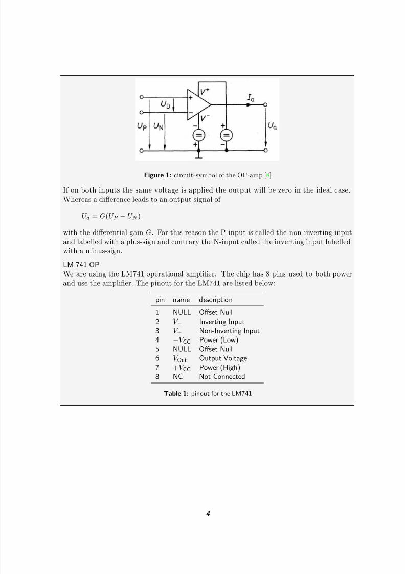
properties of the Op-ampFigure 1 shows the circuit-symbol of an Operational Amplifier. The Input of an Op-ampis a differential amplifier, which amplifies the difference between both inputs.
3
8/4/2019 Analogue-electronics Laboratory Protocol
http://slidepdf.com/reader/full/analogue-electronics-laboratory-protocol 4/43
Figure 1: circuit-symbol of the OP-amp [8]
If on both inputs the same voltage is applied the output will be zero in the ideal case.
Whereas a difference leads to an output signal of
U a = G(U P − U N )
with the differential-gain G. For this reason the P-input is called the non-inverting inputand labelled with a plus-sign and contrary the N-input called the inverting input labelledwith a minus-sign.
LM 741 OPWe are using the LM741 operational amplifier. The chip has 8 pins used to both powerand use the amplifier. The pinout for the LM741 are listed below:
pin name description1 NULL Offset Null2 V − Inverting Input3 V + Non-Inverting Input4 −V CC Power (Low)5 NULL Offset Null6 V Out Output Voltage7 +V CC Power (High)8 NC Not Connected
Table 1: pinout for the LM741
4
8/4/2019 Analogue-electronics Laboratory Protocol
http://slidepdf.com/reader/full/analogue-electronics-laboratory-protocol 5/43
2. Circuits with Operational Amplifiers
2.1. Inverting Operational Amplifier
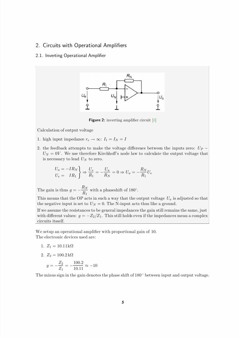
Figure 2: inverting amplifier circuit [8]
Calculation of output voltage
1. high input impedance re →∞: I 1 = I N = I
2. the feedback attempts to make the voltage difference between the inputs zero: U P −U N = 0V . We use therefore Kirchhoff’s node law to calculate the output voltage thatis necessary to lead U N to zero.
U a = −IRN
U e = IR1 ⇒
U eR1
= − U aRN
= 0 ⇒ U a = −RN
R1
U e
The gain is thus g = −RN
R1
with a phaseshift of 180°.
This means that the OP acts in such a way that the output voltage U a is adjusted so thatthe negative input is set to U N = 0. The N-input acts thus like a ground.
If we assume the resistances to be general impedances the gain still remains the same, justwith different values: g = −Z 2/Z 1. This still holds even if the impedances mean a complexcircuits itsself.
We setup an operational amplifier with proportional gain of 10.
The electronic devices used are:
1. Z 1 = 10.11kΩ
2. Z 2 = 100.2 kΩ
g = −Z 2Z 1
= −100.2
10.11≈ −10
The minus sign in the gain denotes the phase shift of 180° between input and output voltage.
5
8/4/2019 Analogue-electronics Laboratory Protocol
http://slidepdf.com/reader/full/analogue-electronics-laboratory-protocol 6/43
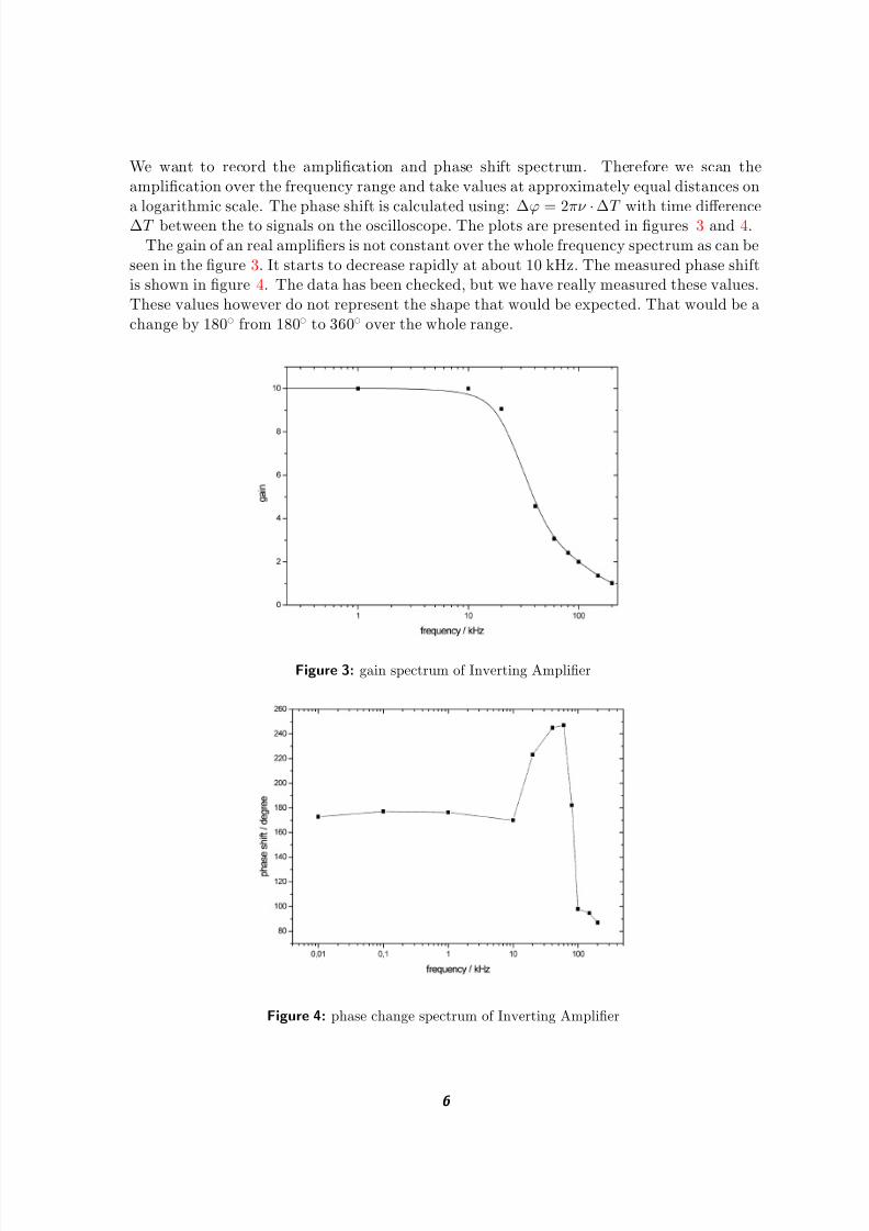
We want to record the amplification and phase shift spectrum. Therefore we scan theamplification over the frequency range and take values at approximately equal distances ona logarithmic scale. The phase shift is calculated using: ∆ϕ = 2πν
·∆T with time difference
∆T between the to signals on the oscilloscope. The plots are presented in figures 3 and 4.The gain of an real amplifiers is not constant over the whole frequency spectrum as can be
seen in the figure 3. It starts to decrease rapidly at about 10 kHz. The measured phase shiftis shown in figure 4. The data has been checked, but we have really measured these values.These values however do not represent the shape that would be expected. That would be achange by 180° from 180° to 360° over the whole range.
Figure 3: gain spectrum of Inverting Amplifier
Figure 4: phase change spectrum of Inverting Amplifier
6
8/4/2019 Analogue-electronics Laboratory Protocol
http://slidepdf.com/reader/full/analogue-electronics-laboratory-protocol 7/43
2.2. Integrator
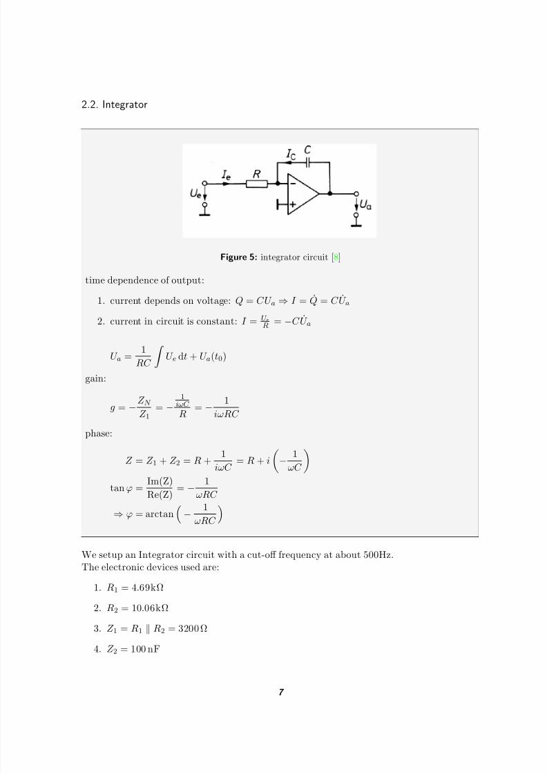
Figure 5: integrator circuit [8]
time dependence of output:
1. current depends on voltage: Q = CU a ⇒ I = Q = C U a
2. current in circuit is constant: I = U eR = −C U a
U a =1
RC
U e dt + U a(t0)
gain:
g = −Z N Z 1 = −
1
iωC R = −1
iωRC
phase:
Z = Z 1 + Z 2 = R +1
iωC = R + i
− 1
ωC
tan ϕ =Im(Z)
Re(Z)= − 1
ωRC
⇒ ϕ = arctan− 1
ωRC
We setup an Integrator circuit with a cut-off frequency at about 500Hz.The electronic devices used are:
1. R1 = 4.69kΩ
2. R2 = 10.06kΩ
3. Z 1 = R1 R2 = 3200 Ω
4. Z 2 = 100 nF
7
8/4/2019 Analogue-electronics Laboratory Protocol
http://slidepdf.com/reader/full/analogue-electronics-laboratory-protocol 8/43
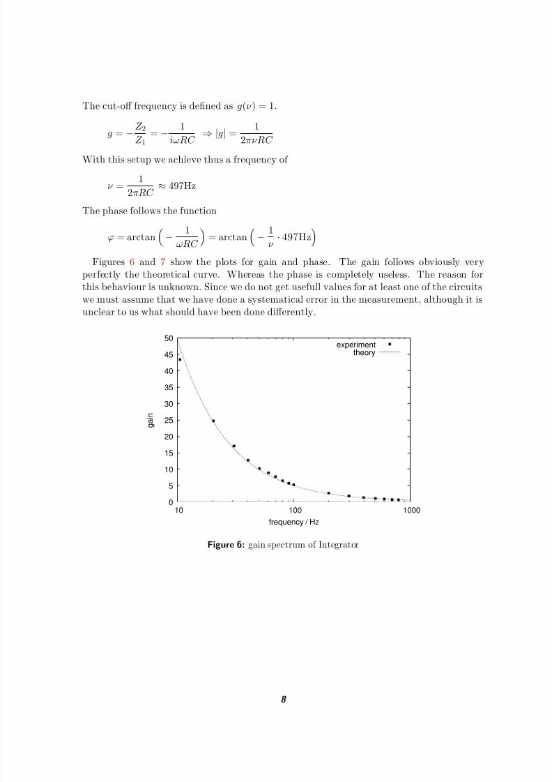
The cut-off frequency is defined as g(ν ) = 1.
g = −Z 2
Z 1 = −1
iωRC ⇒ |g| =
1
2πνRC
With this setup we achieve thus a frequency of
ν =1
2πRC ≈ 497Hz
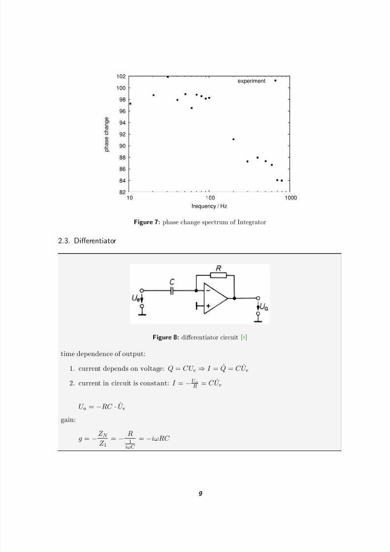
The phase follows the function
ϕ = arctan− 1
ωRC
= arctan
− 1
ν · 497Hz
Figures 6 and 7 show the plots for gain and phase. The gain follows obviously very
perfectly the theoretical curve. Whereas the phase is completely useless. The reason forthis behaviour is unknown. Since we do not get usefull values for at least one of the circuitswe must assume that we have done a systematical error in the measurement, although it isunclear to us what should have been done differently.
0
5
10
15
20
25
30
35
40
45
50
10 100 1000
g a i n
frequency / Hz
experimenttheory
Figure 6: gain spectrum of Integrator
8
8/4/2019 Analogue-electronics Laboratory Protocol
http://slidepdf.com/reader/full/analogue-electronics-laboratory-protocol 9/43
82
84
86
88
90
92
94
96
98
100
102
10 100 1000
p h a s e
c h a n g e
frequency / Hz
experiment
Figure 7: phase change spectrum of Integrator
2.3. Differentiator
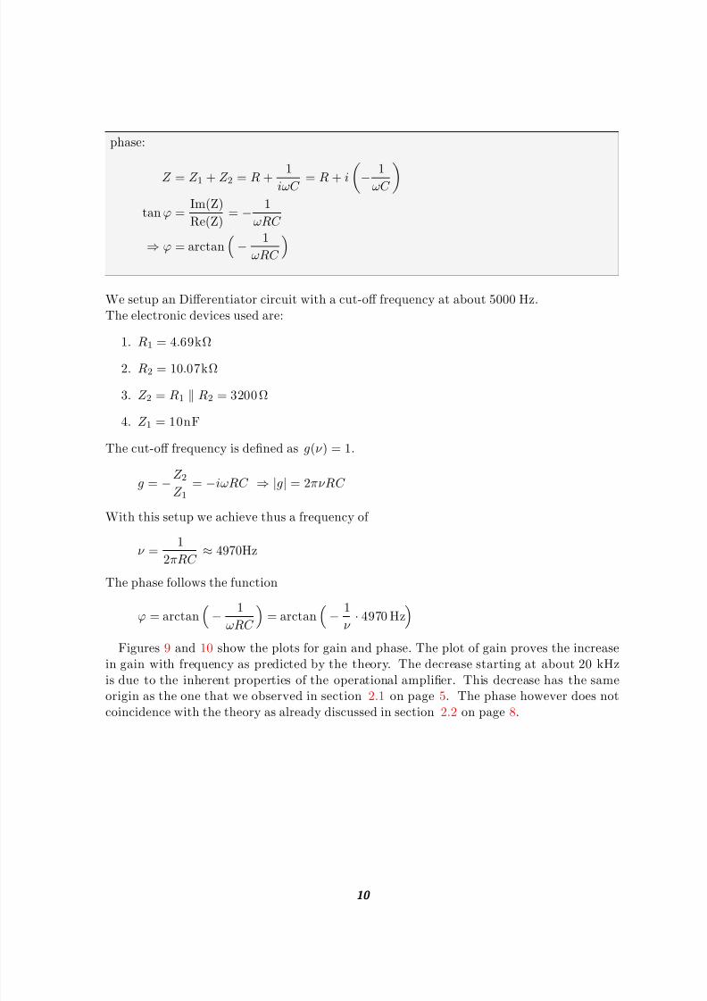
Figure 8: differentiator circuit [8]
time dependence of output:
1. current depends on voltage: Q = CU e ⇒ I = Q = C U e
2. current in circuit is constant: I = −U a
R = C ˙
U e
U a = −RC · U e
gain:
g = −Z N Z 1
= − R1
iωC
= −iωRC
9
8/4/2019 Analogue-electronics Laboratory Protocol
http://slidepdf.com/reader/full/analogue-electronics-laboratory-protocol 10/43
phase:
Z = Z 1 + Z 2 = R + 1iωC = R + i− 1ωC
tan ϕ =
Im(Z)
Re(Z)= − 1
ωRC
⇒ ϕ = arctan− 1
ωRC
We setup an Differentiator circuit with a cut-off frequency at about 5000 Hz.The electronic devices used are:
1. R1 = 4.69kΩ
2. R2 = 10.07kΩ
3. Z 2 = R1 R2 = 3200 Ω
4. Z 1 = 10nF
The cut-off frequency is defined as g(ν ) = 1.
g = −Z 2Z 1
= −iωRC ⇒ |g| = 2πνRC
With this setup we achieve thus a frequency of
ν =1
2πRC ≈ 4970Hz
The phase follows the function
ϕ = arctan− 1
ωRC
= arctan
− 1
ν · 4970 Hz
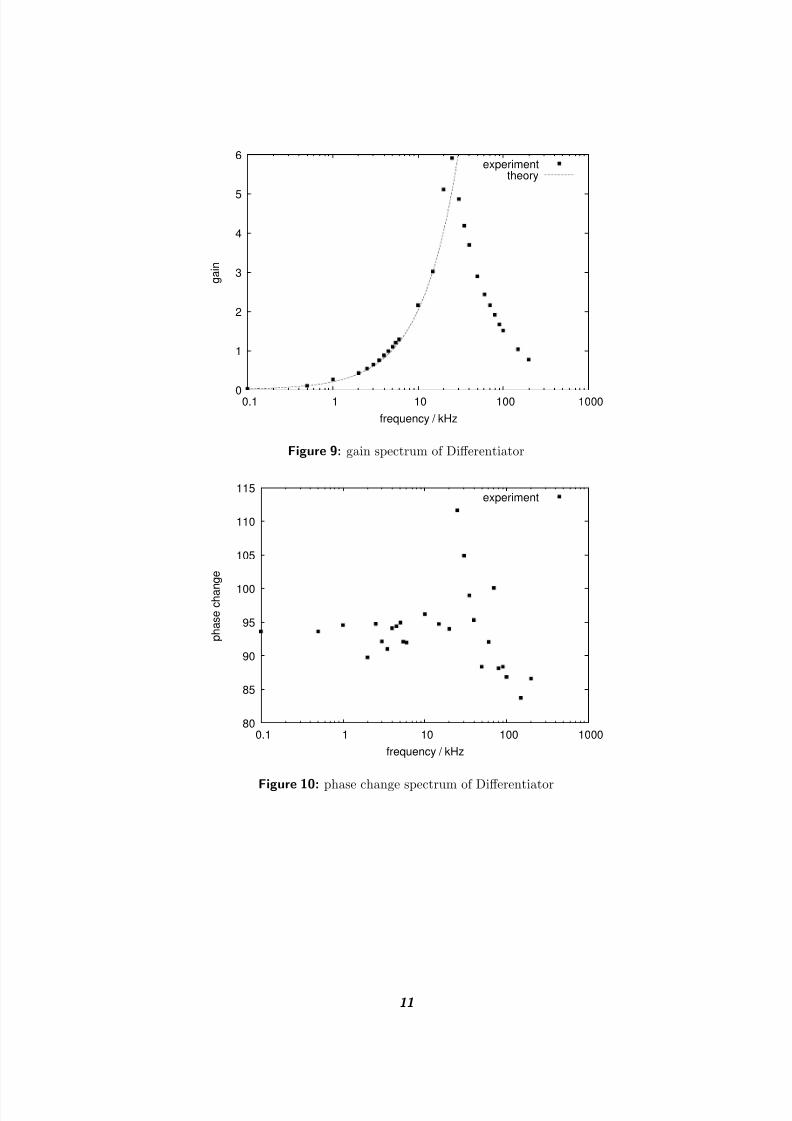
Figures 9 and 10 show the plots for gain and phase. The plot of gain proves the increase
in gain with frequency as predicted by the theory. The decrease starting at about 20 kHzis due to the inherent properties of the operational amplifier. This decrease has the same
origin as the one that we observed in section 2.1 on page 5. The phase however does notcoincidence with the theory as already discussed in section 2.2 on page 8.
10
8/4/2019 Analogue-electronics Laboratory Protocol
http://slidepdf.com/reader/full/analogue-electronics-laboratory-protocol 11/43
0
1
2
3
4
5
6
0.1 1 10 100 1000
g a i n
frequency / kHz
experimenttheory
Figure 9: gain spectrum of Differentiator
80
85
90
95
100
105
110
115
0.1 1 10 100 1000
p h a s e
c h a n
g e
frequency / kHz
experiment
Figure 10: phase change spectrum of Differentiator
11
8/4/2019 Analogue-electronics Laboratory Protocol
http://slidepdf.com/reader/full/analogue-electronics-laboratory-protocol 12/43
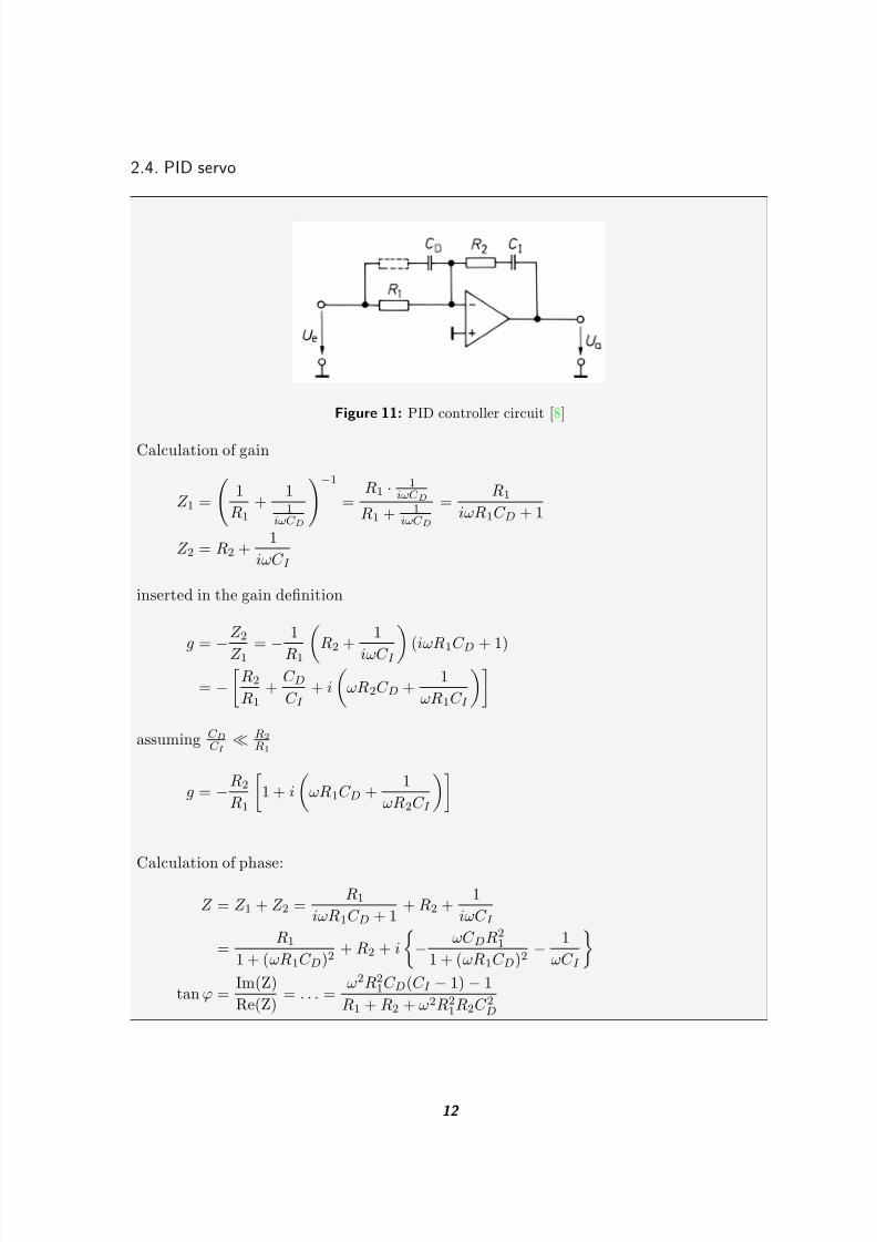
2.4. PID servo
Figure 11: PID controller circuit [8]
Calculation of gain
Z 1 =
1
R1
+11
iωC D
−1=
R1 · 1iωC D
R1 + 1iωC D
=R1
iωR1C D + 1
Z 2 = R2 +1
iωC I
inserted in the gain definition
g =−
Z 2
Z 1=−
1
R1R2 +
1
iωC I (iωR1C
D+ 1)
= −
R2
R1
+C DC I
+ i
ωR2C D +
1
ωR1C I
assuming C DC I R2
R1
g = −R2
R1
1 + i
ωR1C D +
1
ωR2C I
Calculation of phase:
Z = Z 1 + Z 2 =R1
iωR1C D + 1+ R2 +
1
iωC I
=R1
1 + (ωR1C D)2+ R2 + i
− ωC DR2
1
1 + (ωR1C D)2− 1
ωC I
tan ϕ =Im(Z)
Re(Z)= . . . =
ω2R21C D(C I − 1)− 1
R1 + R2 + ω2R21R2C 2D
12
8/4/2019 Analogue-electronics Laboratory Protocol
http://slidepdf.com/reader/full/analogue-electronics-laboratory-protocol 13/43
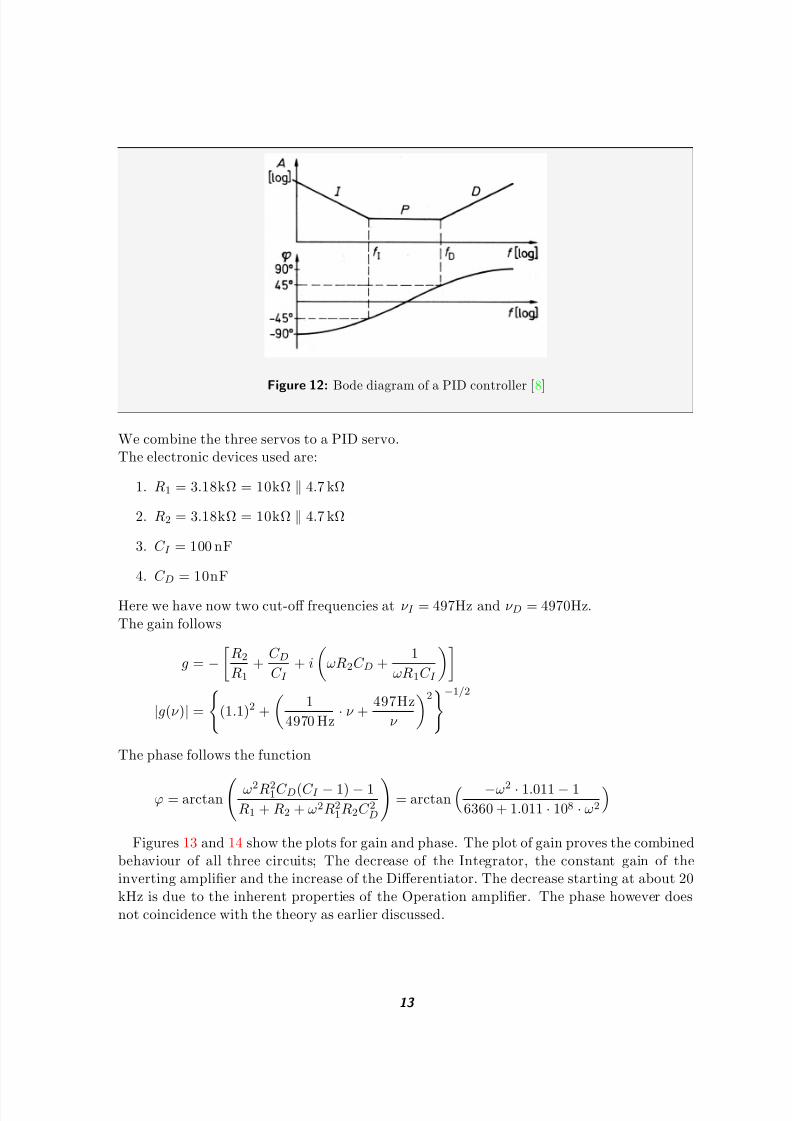
Figure 12: Bode diagram of a PID controller [8]
We combine the three servos to a PID servo.The electronic devices used are:
1. R1 = 3.18kΩ = 10kΩ 4.7 kΩ
2. R2 = 3.18kΩ = 10kΩ 4.7 kΩ
3. C I = 100 nF
4. C D = 10nF
Here we have now two cut-off frequencies at ν I = 497Hz and ν D = 4970Hz.The gain follows
g = −
R2
R1
+C DC I
+ i
ωR2C D +
1
ωR1C I
|g(ν )| =
(1.1)2 +
1
4970 Hz· ν +
497Hz
ν
2−1/2
The phase follows the function
ϕ = arctan
ω2R21C D(C I − 1)− 1R1 + R2 + ω2R2
1R2C 2D
= arctan
−ω2 · 1.011− 16360 + 1.011 · 108 · ω2
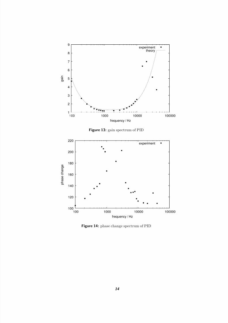
Figures 13 and 14 show the plots for gain and phase. The plot of gain proves the combinedbehaviour of all three circuits; The decrease of the Integrator, the constant gain of theinverting amplifier and the increase of the Differentiator. The decrease starting at about 20kHz is due to the inherent properties of the Operation amplifier. The phase however doesnot coincidence with the theory as earlier discussed.
13
8/4/2019 Analogue-electronics Laboratory Protocol
http://slidepdf.com/reader/full/analogue-electronics-laboratory-protocol 14/43
1
2
3
4
5
6
7
8
9
100 1000 10000 100000
g a i n
frequency / Hz
experimenttheory
Figure 13: gain spectrum of PID
100
120
140
160
180
200
220
100 1000 10000 100000
p h a s e
c h a n
g e
frequency / Hz
experiment
Figure 14: phase change spectrum of PID
14
8/4/2019 Analogue-electronics Laboratory Protocol
http://slidepdf.com/reader/full/analogue-electronics-laboratory-protocol 15/43
3. Digitizing and spectral analysis
3.1. Fourier transformation (theory)
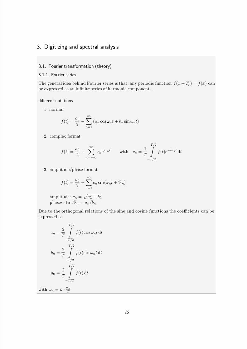
3.1.1. Fourier series
The general idea behind Fourier series is that, any periodic function f (x + T p) = f (x) canbe expressed as an infinite series of harmonic components.
different notations
1. normal
f (t) =
a02 +
∞n=1
(an cos ωnt + bn sin ωnt)
2. complex format
f (t) =a02
+∞
n=−∞cneiωnt with cn =
1
T
T/2 −T/2
f (t)e−iωnt dt
3. amplitude/phase format
f (t) =
a02 +
∞n=1
cn sin(ωnt + Ψn)
amplitude: cn =
a2n + b2nphases: tanΨn = an/bn
Due to the orthogonal relations of the sine and cosine functions the coefficients can beexpressed as
an =2
T
T/2 −T/2
f (t)cos ωnt dt
bn =2
T
T/2 −T/2
f (t)sin ωnt dt
a0 =2
T
T/2 −T/2
f (t) dt
with ωn = n · 2πT
15
8/4/2019 Analogue-electronics Laboratory Protocol
http://slidepdf.com/reader/full/analogue-electronics-laboratory-protocol 16/43
3.1.2. Fourier transformation
For nonperiodic signals and for sections of periodic signals one uses the Fourier transforma-tion instead of the Fourier series. The Fourier transformation and its backtransformationare defined as follows
H (ω) =1√2π
∞ −∞
e−iωth(t) dt
h(t) =1√2π
∞ −∞
eiωtH (ω) dω
A very common way to describe the Fourier transformation is the following
F h(t)
= H (ω)
3.1.3. discrete Fourier transformation
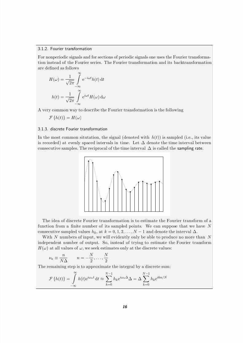
In the most common situtation, the signal (denoted with h(t)) is sampled (i.e., its valueis recorded) at evenly spaced intervals in time. Let ∆ denote the time interval betweenconsecutive samples. The reciprocal of the time interval ∆ is called the sampling rate.
The idea of discrete Fourier transformation is to estimate the Fourier transform of afunction from a finite number of its sampled points. We can suppose that we have N consecutive sampled values hk, at k = 0, 1, 2, . . . , N − 1 and denote the interval ∆.
With N numbers of input, we will evidently only be able to produce no more than N independent number of output. So, instead of trying to estimate the Fourier transformH (ω) at all values of ω, we seek estimates only at the discrete values:
ν n ≡ n
N ∆n = −N
2, . . . ,
N
2
The remaining step is to approximate the integral by a discrete sum:
F h(t) =
∞ −∞
h(t)eiωnt dt ≈N −1k=0
hkeiωn∆∆ = ∆N −1k=0
hkeikn/N
16
8/4/2019 Analogue-electronics Laboratory Protocol
http://slidepdf.com/reader/full/analogue-electronics-laboratory-protocol 17/43
The discrete Fourier transform maps N complex numbers (the hk’s) into N complex num-bers (the H k’s) It does not depend on any dimensional parameter, such as the time scale
∆.
3.1.4. fast Fourier transformation
The fast Fourier transform (FFT) is a discrete Fourier transform algorithm which reducesthe number of computations needed for N points from 2N 2 to 2N lgN , where lg is thebase-2 logarithm. The increase of speed relies on the avoidance of multiple calculations of values that cancel out each other. [1, 2]
3.2. Sampling rates / sampling theorem
The question is, what is the lowest sampling rate at which the signal can be reconstructederror-free? One would expect that if the signal has significant variation then the interval∆ must be small enough to provide an accurate approximation of the signal. Significantsignal variation usually implies that high frequency components are present in the signal.It could therefore be inferred that the higher the frequency of the components present inthe signal, the higher the sampling rate should be. [7]
3.2.1. Nyquist Frequency
For any sampling interval ∆ there is a critical frequency called the Nyquist Frequency givenby
ν c ≡ 1
2∆= 2ν signal (1)
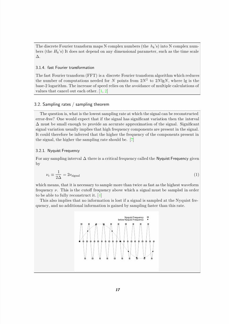
which means, that it is necessary to sample more than twice as fast as the highest waveformfrequency ν . This is the cutoff frequency above which a signal must be sampled in orderto be able to fully reconstruct it. [4]
This also implies that no information is lost if a signal is sampled at the Nyquist fre-quency, and no additional information is gained by sampling faster than this rate.
Nyquist Frequencybelow Nyquist Frequency
17
8/4/2019 Analogue-electronics Laboratory Protocol
http://slidepdf.com/reader/full/analogue-electronics-laboratory-protocol 18/43
3.2.2. Sampling theorem
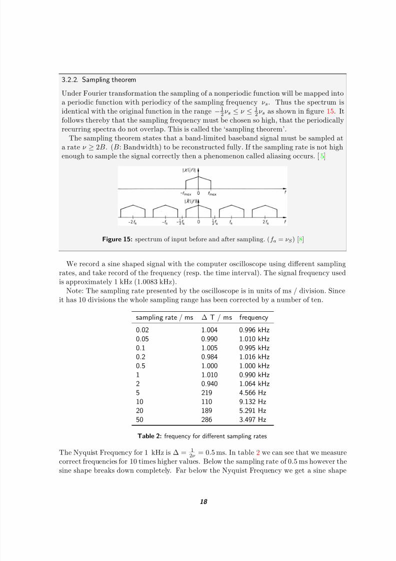
Under Fourier transformation the sampling of a nonperiodic function will be mapped intoa periodic function with periodicy of the sampling frequency ν s. Thus the spectrum isidentical with the original function in the range −1
2ν s ≤ ν ≤ 1
2ν s as shown in figure 15. It
follows thereby that the sampling frequency must be chosen so high, that the periodicallyrecurring spectra do not overlap. This is called the ‘sampling theorem’.
The sampling theorem states that a band-limited baseband signal must be sampled ata rate ν ≥ 2B. (B: Bandwidth) to be reconstructed fully. If the sampling rate is not highenough to sample the signal correctly then a phenomenon called aliasing occurs. [ 5]
Figure 15: spectrum of input before and after sampling. (f a = ν S) [8]
We record a sine shaped signal with the computer oscilloscope using different samplingrates, and take record of the frequency (resp. the time interval). The signal frequency usedis approximately 1 kHz (1.0083 kHz).
Note: The sampling rate presented by the oscilloscope is in units of ms / division. Sinceit has 10 divisions the whole sampling range has been corrected by a number of ten.
sampling rate / ms ∆ T / ms frequency
0.02 1.004 0.996 kHz0.05 0.990 1.010 kHz0.1 1.005 0.995 kHz0.2 0.984 1.016 kHz0.5 1.000 1.000 kHz1 1.010 0.990 kHz2 0.940 1.064 kHz
5 219 4.566 Hz10 110 9.132 Hz20 189 5.291 Hz50 286 3.497 Hz
Table 2: frequency for different sampling rates
The Nyquist Frequency for 1 kHz is ∆ = 12ν = 0.5 ms. In table 2 we can see that we measure
correct frequencies for 10 times higher values. Below the sampling rate of 0.5 ms however thesine shape breaks down completely. Far below the Nyquist Frequency we get a sine shape
18
8/4/2019 Analogue-electronics Laboratory Protocol
http://slidepdf.com/reader/full/analogue-electronics-laboratory-protocol 19/43
signal again, but now with a 1000 times lower frequency. This is due to aliasing. This effectis shown on page 17.
Exemplarily we have taken pictures of the oscilloscope for sampling rates of 0.1, 0.5, 2,100 ms. They are labelled with page 1 to 4 and can be found in the appendix.
3.3. Aliasing
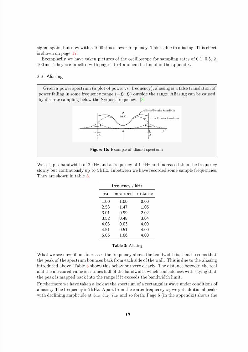
Given a power spectrum (a plot of power vs. frequency), aliasing is a false translation of power falling in some frequency range (−f c, f c) outside the range. Aliasing can be causedby discrete sampling below the Nyquist frequency. [3]
Figure 16: Example of aliased spectrum
We setup a bandwidth of 2 kHz and a frequency of 1 kHz and increased then the frequencyslowly but continuously up to 5 kHz. Inbetween we have recorded some sample frequencies.They are shown in table 3.
frequency / kHz
real measured distance
1.00 1.00 0.002.53 1.47 1.063.01 0.99 2.023.52 0.48 3.044.03 0.03 4.004.51 0.51 4.005.06 1.06 4.00
Table 3: Aliasing
What we see now, if one increases the frequency above the bandwidth is, that it seems thatthe peak of the spectrum bounces back from each side of the wall. This is due to the aliasingintroduced above. Table 3 shows this behaviour very clearly. The distance between the realand the measured value is n-times half of the bandwidth which coincidences with saying thatthe peak is mapped back into the range if it exceeds the bandwidth limit.
Furthermore we have taken a look at the spectrum of a rectangular wave under conditions of aliasing. The frequency is 2 kHz. Apart from the center frequency ω0 we get additional peakswith declining amplitude at 3ω0, 5ω0, 7ω0 and so forth. Page 6 (in the appendix) shows the
19
8/4/2019 Analogue-electronics Laboratory Protocol
http://slidepdf.com/reader/full/analogue-electronics-laboratory-protocol 20/43
spectrum with a bandwidth of 2 kHz. Because of the backreflection all peaks appear in thecenter and form the high background. A similarly spectrum can be found with a bandwidthof 500 Hz (page 7). Here all the peaks overlap near zero because it is half of the originalfrequency.
The false spectrum becomes even more obvious when we use a bandwidth which is not twotimes an integer number of the frequency as with ν = 338.81 Hz and badnwidth B = 5 kHz.This is shown on page 8. The in-between peaks have their origin in the aliasing effect andlead thus to an false spectrum. This behaviour is even increased with a bandwidth of 100 Hzand frequency of 1 kHz (page 9). Here the difference between the ‘main’ peaks amounts only5 Hz instead of 2000 Hz !
At least we take a look at the spectrum of a triangular signal with frequency of 1 kHzand bandwidth 2 kHz (page 10). One should expect a picture like the one on page 6 for therectangular signal. This picture however can easily be mistaken with sine signal as on page5. The faster decrease of the amplitude leads to a much lower background, so that we seeonly one peak.
The shown examples demonstrate very clearly why it is very important to choose the correctbandwidth to record the correct spectrum. To get around of the aliasing effect filters arevery common to reduce the bandwidth-passing frequencies.
20
8/4/2019 Analogue-electronics Laboratory Protocol
http://slidepdf.com/reader/full/analogue-electronics-laboratory-protocol 21/43
3.4. Spectral analysis of sine, rectangular and triangular signals
3.4.1. sine
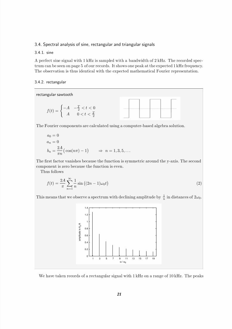
A perfect sine signal with 1 kHz is sampled with a bandwidth of 2 kHz. The recorded spec-trum can be seen on page 5 of our records. It shows one peak at the expected 1 kHz frequency.The observation is thus identical with the expected mathematical Fourier representation.
3.4.2. rectangular
rectangular sawtooth
f (t) = −A −T
2< t < 0
A 0 < t <T 2
The Fourier components are calculated using a computer-based algebra solution.
a0 = 0
an = 0
bn =2A
πn
cos(nπ)− 1
⇒ n = 1, 3, 5, . . .
The first factor vanishes because the function is symmetric around the y-axis. The secondcomponent is zero because the function is even.
Thus follows
f (t) =2A
π
∞n=1
1
nsin
(2n− 1)ω0t
(2)
This means that we observe a spectrum with declining amplitude by 1n in distances of 2ω0.
0
0.2
0.4
0.6
0.8
1
1.2
1.4
1 3 5 7 9 11 13 15 17 19
a m p l i t u d e i n A n
/ A
ω / ω0
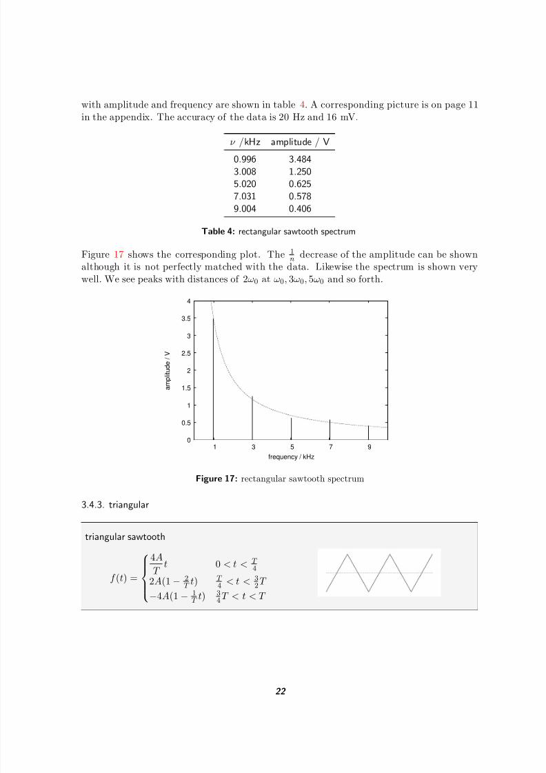
We have taken records of a rectangular signal with 1 kHz on a range of 10 kHz. The peaks
21
8/4/2019 Analogue-electronics Laboratory Protocol
http://slidepdf.com/reader/full/analogue-electronics-laboratory-protocol 22/43
with amplitude and frequency are shown in table 4. A corresponding picture is on page 11in the appendix. The accuracy of the data is 20 Hz and 16 mV.
ν /kHz amplitude / V
0.996 3.4843.008 1.2505.020 0.6257.031 0.5789.004 0.406
Table 4: rectangular sawtooth spectrum
Figure 17 shows the corresponding plot. The 1n decrease of the amplitude can be shown
although it is not perfectly matched with the data. Likewise the spectrum is shown verywell. We see peaks with distances of 2ω0 at ω0, 3ω0, 5ω0 and so forth.
0
0.5
1
1.5
2
2.5
3
3.5
4
1 3 5 7 9
a m p l i t u d e / V
frequency / kHz
Figure 17: rectangular sawtooth spectrum
3.4.3. triangular
triangular sawtooth
f (t) =
4A
T t 0 < t < T
4
2A(1− 2T t) T
4< t < 3
2T
−4A(1− 1T t) 3
4T < t < T
22
8/4/2019 Analogue-electronics Laboratory Protocol
http://slidepdf.com/reader/full/analogue-electronics-laboratory-protocol 23/43
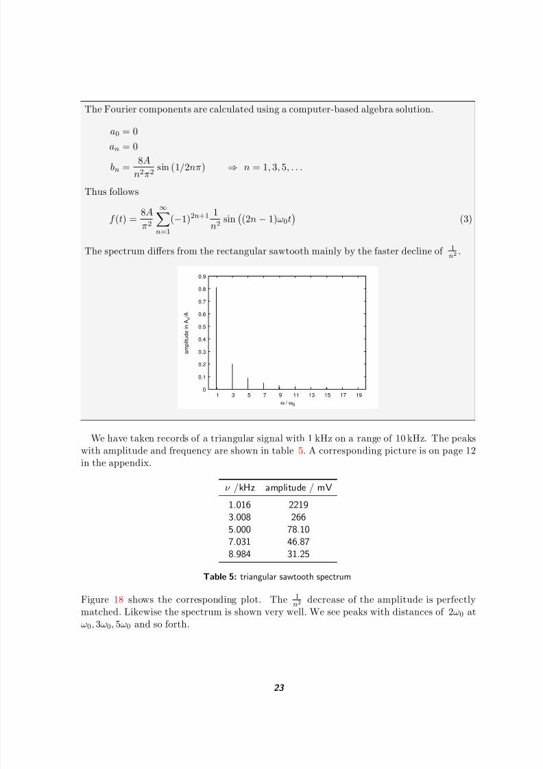
The Fourier components are calculated using a computer-based algebra solution.
a0 = 0an = 0
bn =8A
n2π2sin (1/2nπ) ⇒ n = 1, 3, 5, . . .
Thus follows
f (t) =8A
π2
∞n=1
(−1)2n+11
n2sin
(2n− 1)ω0t
(3)
The spectrum differs from the rectangular sawtooth mainly by the faster decline of 1
n2.
0
0.1
0.2
0.3
0.4
0.5
0.6
0.7
0.8
0.9
1 3 5 7 9 11 13 15 17 19
a m p l i t u d e i n A n
/ A
ω / ω0
We have taken records of a triangular signal with 1 kHz on a range of 10 kHz. The peakswith amplitude and frequency are shown in table 5. A corresponding picture is on page 12in the appendix.
ν /kHz amplitude / mV
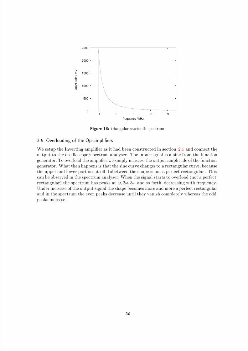
1.016 22193.008 2665.000 78.10
7.031 46.878.984 31.25
Table 5: triangular sawtooth spectrum
Figure 18 shows the corresponding plot. The 1
n2decrease of the amplitude is perfectly
matched. Likewise the spectrum is shown very well. We see peaks with distances of 2ω0 atω0, 3ω0, 5ω0 and so forth.
23
8/4/2019 Analogue-electronics Laboratory Protocol
http://slidepdf.com/reader/full/analogue-electronics-laboratory-protocol 24/43
0
500
1000
1500
2000
2500
1 3 5 7 9
a m p l i t u d e / m V
frequency / kHz
Figure 18: triangular sawtooth spectrum
3.5. Overloading of the Op-amplifiers
We setup the Inverting amplifier as it had been constructed in section 2.1 and connect theoutput to the oscilloscope/spectrum analyser. The input signal is a sine from the functiongenerator. To overload the amplifier we simply increase the output amplitude of the functiongenerator. What then happens is that the sine curve changes to a rectangular curve, becausethe upper and lower part is cut-off. Inbetween the shape is not a perfect rectangular . Thiscan be observed in the spectrum analyser. When the signal starts to overload (not a perfect
rectangular) the spectrum has peaks at ω, 2ω, 3ω and so forth, decreasing with frequency.Under increase of the output signal the shape becomes more and more a perfect rectangularand in the spectrum the even peaks decrease until they vanish completely whereas the oddpeaks increase.
24
8/4/2019 Analogue-electronics Laboratory Protocol
http://slidepdf.com/reader/full/analogue-electronics-laboratory-protocol 25/43
4. Modulation
4.1. Frequency modulation (FM)
a m p l i t u d e
time
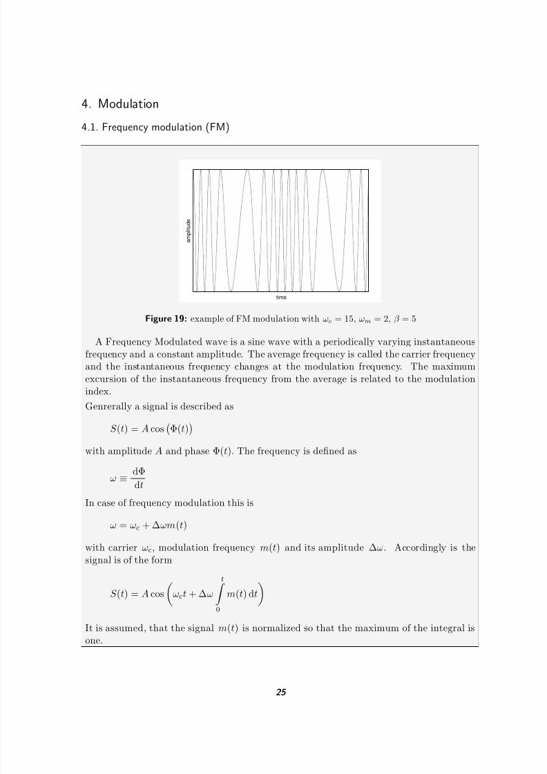
Figure 19: example of FM modulation with ωc = 15, ωm = 2, β = 5
A Frequency Modulated wave is a sine wave with a periodically varying instantaneousfrequency and a constant amplitude. The average frequency is called the carrier frequencyand the instantaneous frequency changes at the modulation frequency. The maximumexcursion of the instantaneous frequency from the average is related to the modulationindex.
Genrerally a signal is described as
S (t) = A cos
Φ(t)
with amplitude A and phase Φ(t). The frequency is defined as
ω ≡ dΦ
dt
In case of frequency modulation this is
ω = ωc + ∆ωm(t)
with carrier ωc, modulation frequency m(t) and its amplitude ∆ω. Accordingly is thesignal is of the form
S (t) = A cos
ωct + ∆ω
t 0
m(t) dt
It is assumed, that the signal m(t) is normalized so that the maximum of the integral isone.
25
8/4/2019 Analogue-electronics Laboratory Protocol
http://slidepdf.com/reader/full/analogue-electronics-laboratory-protocol 26/43
For a modulation signal of the form
m(t) = cos(ωmt)
the time dependent frequency is
ω = ωc + ∆ω cos(ωmt)
and the phase
Φ = ωct +∆ω
ωmcos(ωmt)
The ratio β = ∆ωωm
is called the modulation index.
The entire expression is thus
S (t) = A cos
ωct + β sin(ωmt)
(4)
The frequency spectrum can be found by rewriting the above expression as a sum of components of constant frequency using the properties of the Bessel Functions. This gives:
S (t) = A
J 0(β ) sin(ωct)
+ J 1(β ) [sin(ωc + ωm)t− sin(ωc − ωm)t]
+ J 2(β ) [sin(ωc + 2ωm)t + sin(ωc − 2ωm)t]
+ J 3(β ) [sin(ωc
+ 3ωm
)t−
sin(ωc −
3ωm
)t]
+ . . .
(5)
This expression implies that the FM spectrum consists of a component at ωc and an infinitenumber of lines at ωc ± nωm and that the amplitude of the components are given by theBessel functions. [6]
We use both function generators to generate a frequency modulated signal. Thereby onegenerator is the input for the other generator.
To observe the effect of frequency modulation on the oscilloscope we scanned a few varietiesof frequencies and modulation indices. Finally we have set up a carrier frequency of 25 kHz
and a modulation frequency of 625 Hz with a high amplitude of the modulation signal (highmodulation index). The plot can be found on page 13 in the appendix. In the range wherethe frequency goes to zero the modulation value is the highest, whereas in the other rangethe wave of the modulation goes through zero and thus the frequency is more or less thecarrier frequency. If one increases the amplitude the number of periods will increase, but theoverall shape stays the same. The according spectrum has equal high and low frequencies(white spectrum).
To observe a typical FM spectrum we had to reduce the amplitude of the modulationsignal by 20 dB. The carrier frequency is now set to 25 kHz and the modulation frequencyto 5 kHz. If we vary the modulation index (resp. the modulation-amplitude) we find that
26
8/4/2019 Analogue-electronics Laboratory Protocol
http://slidepdf.com/reader/full/analogue-electronics-laboratory-protocol 27/43
with low modulation index we have only the peak from the carrier signal. Whereas when weincrease the modulation index the carrier peak in the middle decreases and symmetricallypeaks appear on both sides growing with frequency. This behaviour is shown on pages 14-16in the appendix. (Note: The printout of the last page is did not match with the screen. Thelow amplitude of the peaks is due to the program or the printer)
Finally we are interested in the spacing between the peaks. The expansion into Besselfunc-tions shows that we should expect an equal spacing between the peaks by the modulationfrequency independently of the modulation index. Therefore we have measured the spacingfor different indices. The data is shown in table 6. One can see clearly that the spacing isaccording to the theory. Pages 14-16 show the according spectrum.
frequency peak
modulation index ω1 ω2 ω3 ω4 ω5 ω6 ω7
8.000 · 10−5 15.82 20.8 25.78 30.76 35.841.876 · 10−4 10.44 15.43 20.5 25.58 30.56 35.64 40.622.218 · 10−4 10.64 15.72 20.7 25.87 30.76 35.84 40.91
frequency peak spacing
ω2 − ω1 ω3 − ω2 ω4 − ω3 ω5 − ω4 ω6 − ω5 ω7 − ω6
8.000 · 10−5 4.98 4.98 4.98 5.081.876 · 10−4 4.99 5.07 5.08 4.98 5.08 4.982.218 · 10−4 5.08 4.98 5.17 4.89 5.08 5.07
Table 6: modulation index
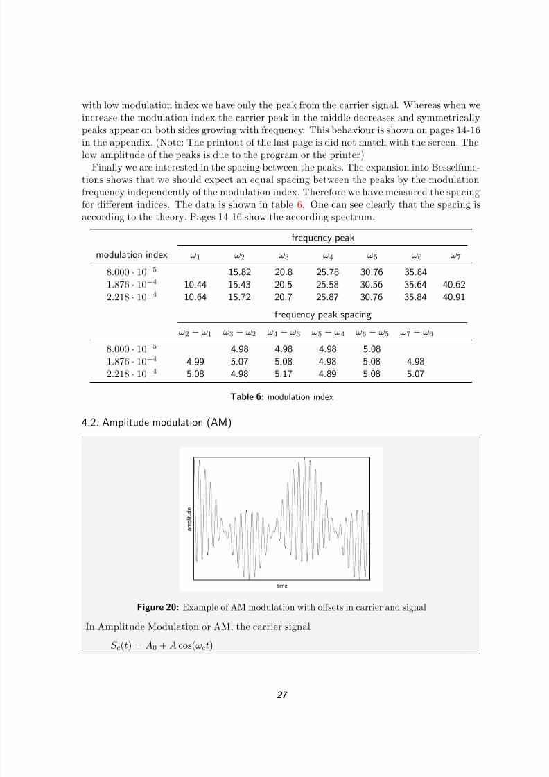
4.2. Amplitude modulation (AM)
a m p l i t u d e
time
Figure 20: Example of AM modulation with offsets in carrier and signal
In Amplitude Modulation or AM, the carrier signal
S c(t) = A0 + A cos(ωct)
27
8/4/2019 Analogue-electronics Laboratory Protocol
http://slidepdf.com/reader/full/analogue-electronics-laboratory-protocol 28/43
has its amplitude A modulated by the (lower frequency) message signal m(t). We assumea harmonic oscillating modulation
m(t) = B0 + B cos(ωmt)
Then follows for the linear amplitude modulated signal
S (t) = m(t) · S (t)
= A0B cos(ωmt) + B0A cos(ωct) + AB cos(ωct) · cos(ωmt)
= A0B cos(ωmt) + B0A cos(ωct)
+1
2AB cos
(ωc + ωm)t
+
1
2AB cos
(ωc − ωm)t
(6)
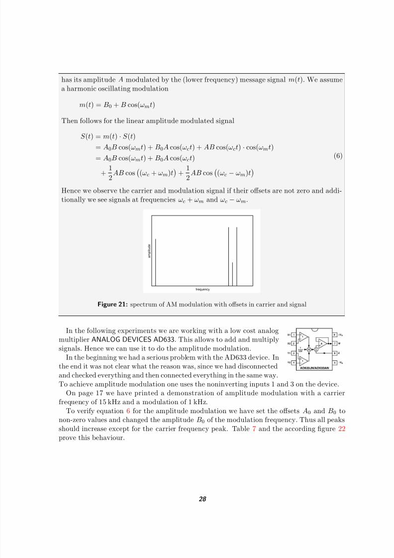
Hence we observe the carrier and modulation signal if their offsets are not zero and addi-tionally we see signals at frequencies ωc + ωm and ωc − ωm.
a m p l i t u d e
frequency
Figure 21: spectrum of AM modulation with offsets in carrier and signal
In the following experiments we are working with a low cost analogmultiplier ANALOG DEVICES AD633. This allows to add and multiplysignals. Hence we can use it to do the amplitude modulation.
In the beginning we had a serious problem with the AD633 device. Inthe end it was not clear what the reason was, since we had disconnectedand checked everything and then connected everything in the same way.To achieve amplitude modulation one uses the noninverting inputs 1 and 3 on the device.
On page 17 we have printed a demonstration of amplitude modulation with a carrierfrequency of 15 kHz and a modulation of 1 kHz.
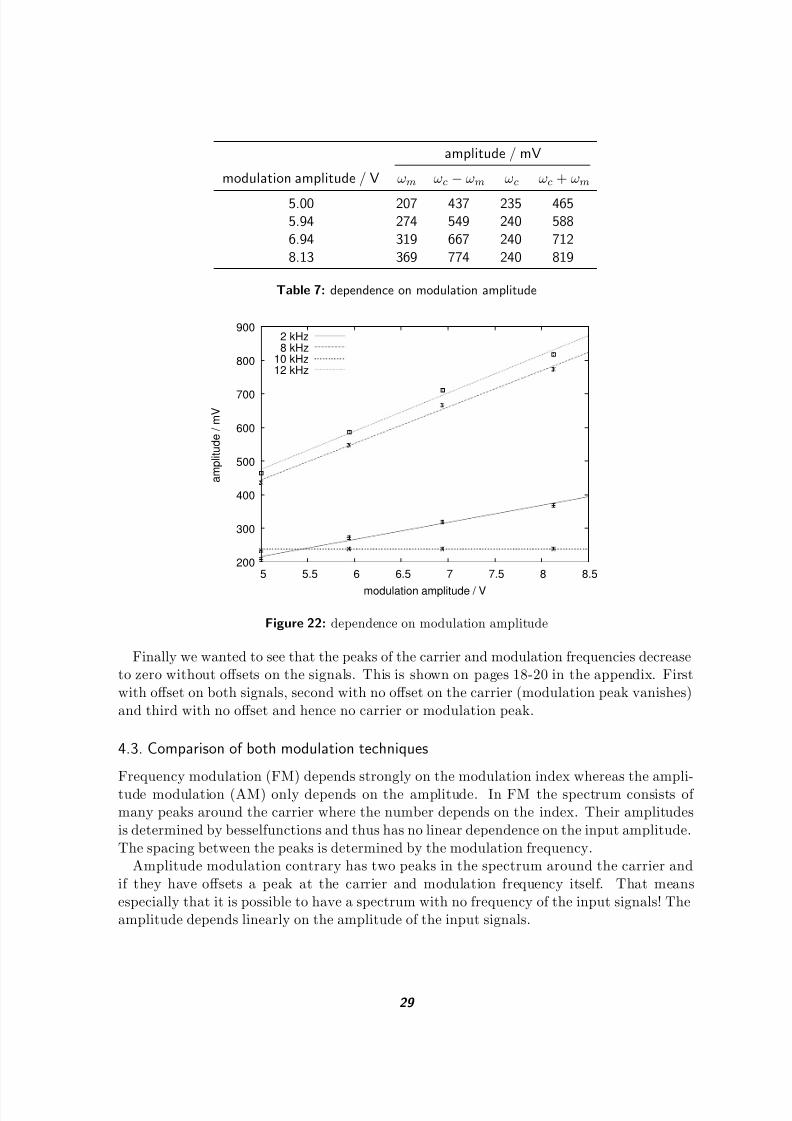
To verify equation 6 for the amplitude modulation we have set the offsets A0 and B0 tonon-zero values and changed the amplitude B0 of the modulation frequency. Thus all peaksshould increase except for the carrier frequency peak. Table 7 and the according figure 22prove this behaviour.
28
8/4/2019 Analogue-electronics Laboratory Protocol
http://slidepdf.com/reader/full/analogue-electronics-laboratory-protocol 29/43
amplitude / mV
modulation amplitude / V ωm ωc
−ωm ωc ωc + ωm
5.00 207 437 235 4655.94 274 549 240 5886.94 319 667 240 7128.13 369 774 240 819
Table 7: dependence on modulation amplitude
200
300
400
500
600
700
800
900
5 5.5 6 6.5 7 7.5 8 8.5
a m p l i t u d e / m V
modulation amplitude / V
2 kHz8 kHz
10 kHz12 kHz
Figure 22: dependence on modulation amplitude
Finally we wanted to see that the peaks of the carrier and modulation frequencies decreaseto zero without offsets on the signals. This is shown on pages 18-20 in the appendix. Firstwith offset on both signals, second with no offset on the carrier (modulation peak vanishes)and third with no offset and hence no carrier or modulation peak.
4.3. Comparison of both modulation techniques
Frequency modulation (FM) depends strongly on the modulation index whereas the ampli-tude modulation (AM) only depends on the amplitude. In FM the spectrum consists of many peaks around the carrier where the number depends on the index. Their amplitudesis determined by besselfunctions and thus has no linear dependence on the input amplitude.The spacing between the peaks is determined by the modulation frequency.
Amplitude modulation contrary has two peaks in the spectrum around the carrier andif they have offsets a peak at the carrier and modulation frequency itself. That meansespecially that it is possible to have a spectrum with no frequency of the input signals! Theamplitude depends linearly on the amplitude of the input signals.
29
8/4/2019 Analogue-electronics Laboratory Protocol
http://slidepdf.com/reader/full/analogue-electronics-laboratory-protocol 30/43
5. Noise
Loosely, noise is a disturbance tending to interfere with the normal operation of a device or
system. It is an undesired disturbance within the frequency band of interest, that affects asignal and may distort the information carried by the signal.
5.1. Different noise processes
A noise is a random signal of known statistical properties of amplitude, distribution,and spectral density. Generally speaking, there are five different kinds of noise: thermal noise, shot noise, 1/f noise (technical noise), generation and combination noise especially in semiconductors, and white noise
Although the production mechanisms vary, generally, the noises are produced in a certainperiod of time t, called the characteristic time. And the sampling time is T , f is thesampling frequency, defined by f = 1/T . So for different t and T relationships, the spectraldependence of the noise power ω(f ) is different.
1. t T : ω(f ) ∝ f 0
2. t T : ω(f ) ∝ f −2
3. t ≈ T : ω(f ) ∝ f −1
For example, 1 can be white noise, 2 can be generation and recombination noise, 3 can betechnical noise P (f )
∝f −1, for the 3, since all the noise processes should have almost the
same characteristic time, so the spectral range is quite narrow.
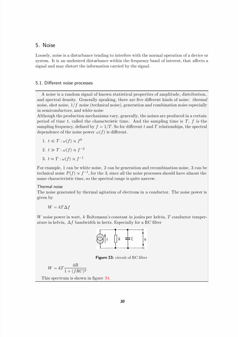
Thermal noiseThe noise generated by thermal agitation of electrons in a conductor. The noise power isgiven by
W = kT ∆f
W noise power in watt, k Boltzmann’s constant in joules per kelvin, T conductor temper-ature in kelvin, ∆f bandwidth in hertz. Especially for a RC filter
Figure 23: circuit of RC filter
W = kT 4R
1 + (f RC )2
This spectrum is shown in figure 24.
30
8/4/2019 Analogue-electronics Laboratory Protocol
http://slidepdf.com/reader/full/analogue-electronics-laboratory-protocol 31/43
Figure 24: spectrum of thermal noise in RC filter circuit
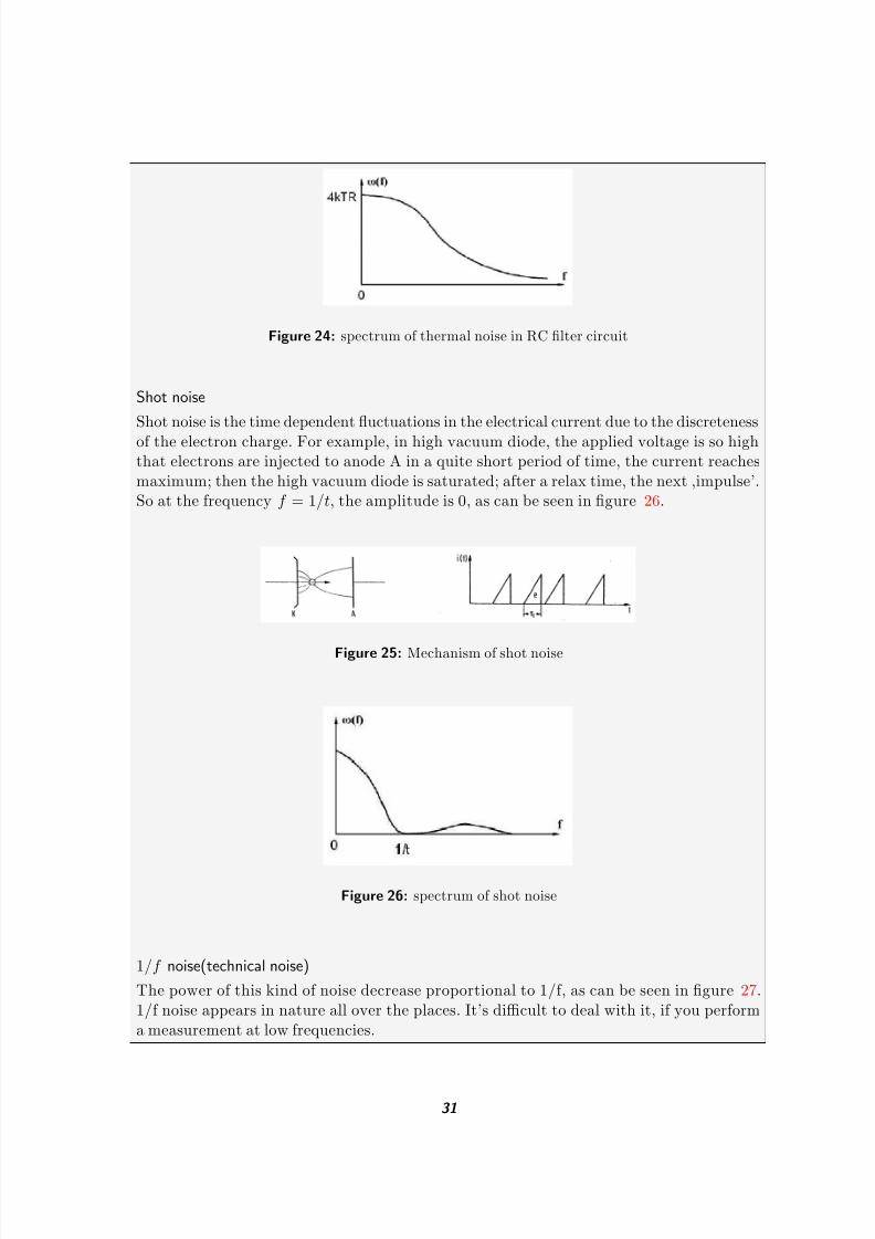
Shot noise
Shot noise is the time dependent fluctuations in the electrical current due to the discretenessof the electron charge. For example, in high vacuum diode, the applied voltage is so highthat electrons are injected to anode A in a quite short period of time, the current reachesmaximum; then the high vacuum diode is saturated; after a relax time, the next ,impulse’.So at the frequency f = 1/t, the amplitude is 0, as can be seen in figure 26.
Figure 25: Mechanism of shot noise
Figure 26: spectrum of shot noise
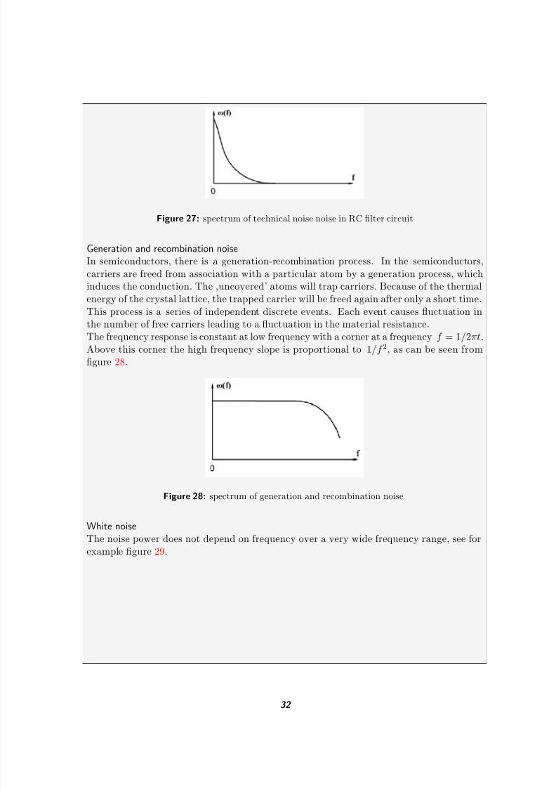
1/f noise(technical noise)
The power of this kind of noise decrease proportional to 1/f, as can be seen in figure 27.1/f noise appears in nature all over the places. It’s difficult to deal with it, if you performa measurement at low frequencies.
31
8/4/2019 Analogue-electronics Laboratory Protocol
http://slidepdf.com/reader/full/analogue-electronics-laboratory-protocol 32/43
Figure 27: spectrum of technical noise noise in RC filter circuit
Generation and recombination noiseIn semiconductors, there is a generation-recombination process. In the semiconductors,
carriers are freed from association with a particular atom by a generation process, whichinduces the conduction. The ,uncovered’ atoms will trap carriers. Because of the thermalenergy of the crystal lattice, the trapped carrier will be freed again after only a short time.This process is a series of independent discrete events. Each event causes fluctuation inthe number of free carriers leading to a fluctuation in the material resistance.The frequency response is constant at low frequency with a corner at a frequency f = 1/2πt.Above this corner the high frequency slope is proportional to 1/f 2, as can be seen fromfigure 28.
Figure 28: spectrum of generation and recombination noise
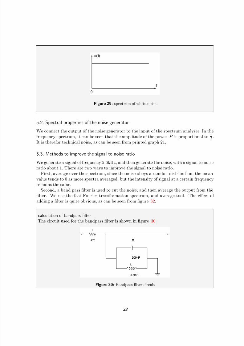
White noiseThe noise power does not depend on frequency over a very wide frequency range, see for
example figure 29.
32
8/4/2019 Analogue-electronics Laboratory Protocol
http://slidepdf.com/reader/full/analogue-electronics-laboratory-protocol 33/43
Figure 29: spectrum of white noise
5.2. Spectral properties of the noise generator
We connect the output of the noise generator to the input of the spectrum analyser. In thefrequency spectrum, it can be seen that the amplitude of the power P is proportional to 1
f .It is therefor technical noise, as can be seen from printed graph 21.
5.3. Methods to improve the signal to noise ratio
We generate a signal of frequency 5.6kHz, and then generate the noise, with a signal to noiseratio about 1. There are two ways to improve the signal to noise ratio.
First, average over the spectrum, since the noise obeys a ramdon distribution, the meanvalue tends to 0 as more spectra averaged; but the intensity of signal at a certain frequencyremains the same.
Second, a band pass filter is used to cut the noise, and then average the output from thefilter. We use the fast Fourier transformation spectrum, and average tool. The effect of adding a filter is quite obvious, as can be seen from figure 32.
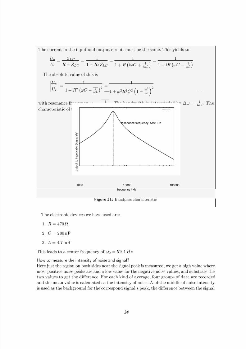
calculation of bandpass filterThe circuit used for the bandpass filter is shown in figure 30.
R
470 C
200nF
C
200nF
C
200nF
C
200nF
L
4.7mH
Figure 30: Bandpass filter circuit
33
8/4/2019 Analogue-electronics Laboratory Protocol
http://slidepdf.com/reader/full/analogue-electronics-laboratory-protocol 34/43
The current in the input and output circuit must be the same. This yields to
U a
U i =Z LC
R + Z LC =1
1 + R/Z LC =1
1 + R
iωC + 1iωL
=1
1 + iR
ωC − 1ωL
The absolute value of this isU a
U i
=1
1 + R2
ωC − 1ωL
2 =1
1 + ω2R2C 2
1− ω20
ω2
2with resonance frequency ω0 = 1√
LC . The bandwidth is determinded by ∆ω = 1
RC . The
characteristic of this filter is shown in figure 31
1000 10000 100000
o u t p u t t o
i n p u t r a t i o
( l o g
s c a l e )
frequency / Hz
resonance frequency: 5191 Hz
Figure 31: Bandpass characteristic
The electronic devices we have used are:
1. R = 470 Ω
2. C = 200 nF
3. L = 4.7 mHThis leads to a center frequency of ω0 = 5191 Hz
How to measure the intensity of noise and signal?Here just the region on both sides near the signal peak is measured, we get a high value wheremost positive noise peaks are and a low value for the negative noise vallies, and substrate thetwo values to get the difference. For each kind of average, four groups of data are recordedand the mean value is calculated as the intensity of noise. And the middle of noise intensityis used as the background for the correspond signal’s peak, the difference between the signal
34
8/4/2019 Analogue-electronics Laboratory Protocol
http://slidepdf.com/reader/full/analogue-electronics-laboratory-protocol 35/43
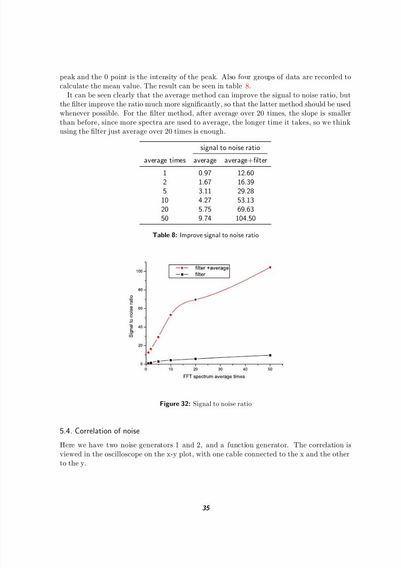
peak and the 0 point is the intensity of the peak. Also four groups of data are recorded tocalculate the mean value. The result can be seen in table 8.
It can be seen clearly that the average method can improve the signal to noise ratio, butthe filter improve the ratio much more significantly, so that the latter method should be usedwhenever possible. For the filter method, after average over 20 times, the slope is smallerthan before, since more spectra are used to average, the longer time it takes, so we thinkusing the filter just average over 20 times is enough.
signal to noise ratio
average times average average+filter
1 0.97 12.602 1.67 16.395 3.11 29.28
10 4.27 53.1320 5.75 69.6350 9.74 104.50
Table 8: Improve signal to noise ratio
0 1 0 2 0 3 0 4 0 5 0
S
g
n
a
t
o
n
o
s
e
r
a
t
o
F F T s p e c t r u m a v e r a g e t i m e s
f i l t e r + a v e r a g e
f i l t e r
Figure 32: Signal to noise ratio
5.4. Correlation of noise
Here we have two noise generators 1 and 2, and a function generator. The correlation isviewed in the oscilloscope on the x-y plot, with one cable connected to the x and the otherto the y.
35
8/4/2019 Analogue-electronics Laboratory Protocol
http://slidepdf.com/reader/full/analogue-electronics-laboratory-protocol 36/43
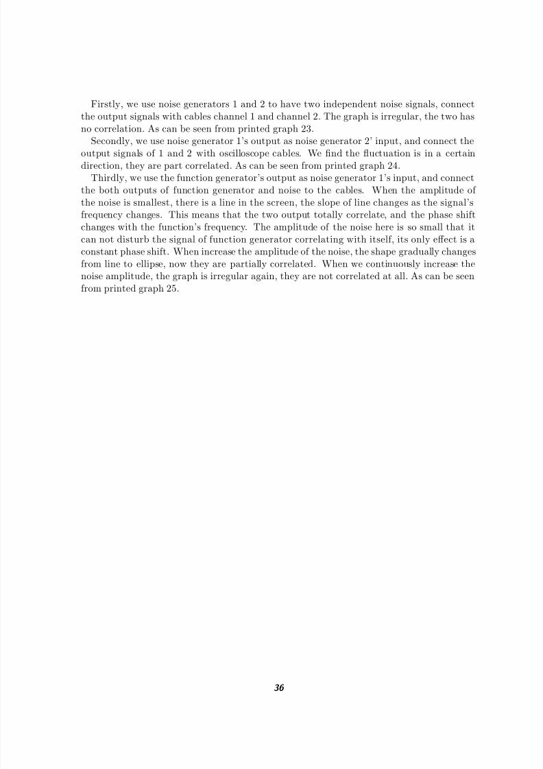
Firstly, we use noise generators 1 and 2 to have two independent noise signals, connectthe output signals with cables channel 1 and channel 2. The graph is irregular, the two hasno correlation. As can be seen from printed graph 23.
Secondly, we use noise generator 1’s output as noise generator 2’ input, and connect theoutput signals of 1 and 2 with oscilloscope cables. We find the fluctuation is in a certaindirection, they are part correlated. As can be seen from printed graph 24.
Thirdly, we use the function generator’s output as noise generator 1’s input, and connectthe both outputs of function generator and noise to the cables. When the amplitude of the noise is smallest, there is a line in the screen, the slope of line changes as the signal’sfrequency changes. This means that the two output totally correlate, and the phase shiftchanges with the function’s frequency. The amplitude of the noise here is so small that itcan not disturb the signal of function generator correlating with itself, its only effect is aconstant phase shift. When increase the amplitude of the noise, the shape gradually changesfrom line to ellipse, now they are partially correlated. When we continuously increase thenoise amplitude, the graph is irregular again, they are not correlated at all. As can be seenfrom printed graph 25.
36
8/4/2019 Analogue-electronics Laboratory Protocol
http://slidepdf.com/reader/full/analogue-electronics-laboratory-protocol 37/43
A. measuring data
A.1. Operational Amplifiers
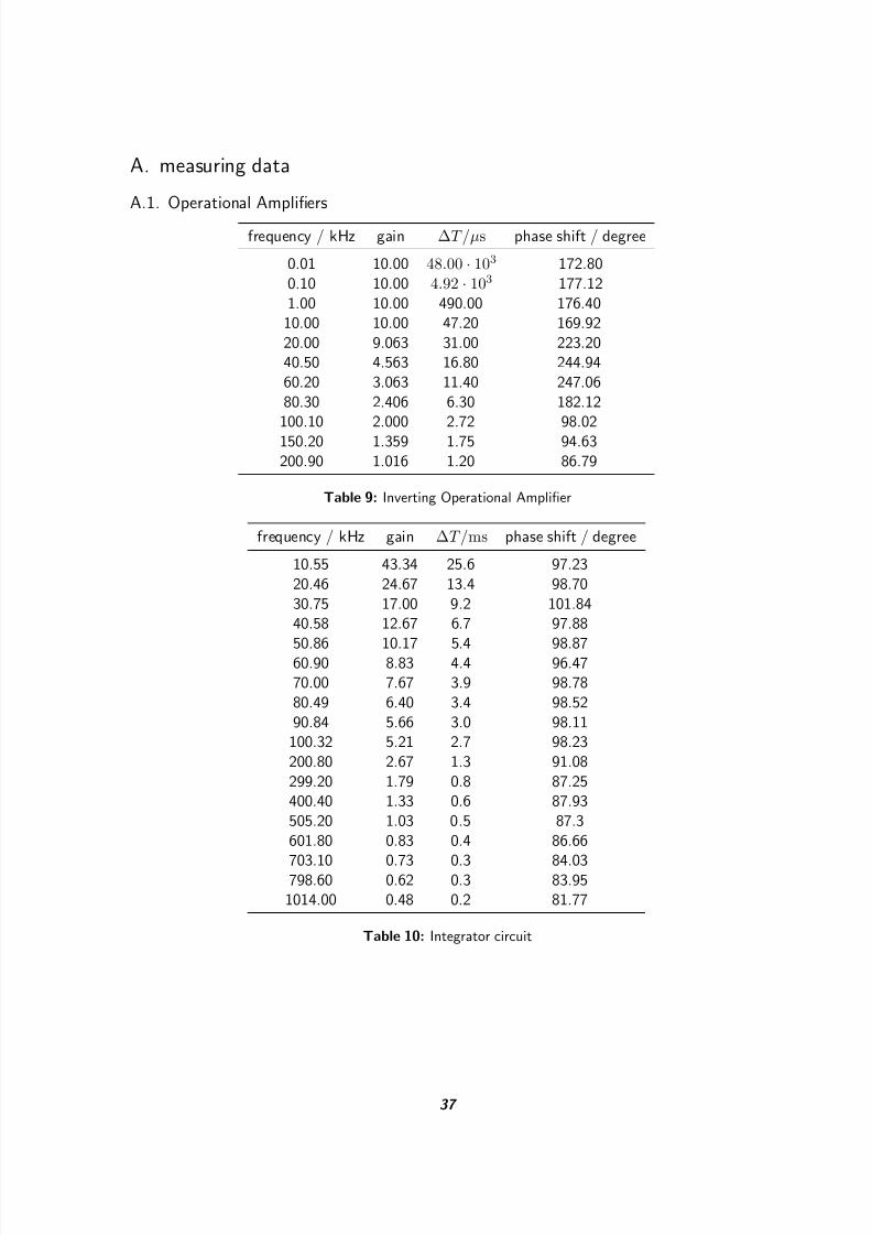
frequency / kHz gain ∆T /µs phase shift / degree
0.01 10.00 48.00 · 103 172.800.10 10.00 4.92 · 103 177.121.00 10.00 490.00 176.40
10.00 10.00 47.20 169.9220.00 9.063 31.00 223.2040.50 4.563 16.80 244.9460.20 3.063 11.40 247.0680.30 2.406 6.30 182.12
100.10 2.000 2.72 98.02150.20 1.359 1.75 94.63200.90 1.016 1.20 86.79
Table 9: Inverting Operational Amplifier
frequency / kHz gain ∆T /ms phase shift / degree
10.55 43.34 25.6 97.2320.46 24.67 13.4 98.7030.75 17.00 9.2 101.8440.58 12.67 6.7 97.88
50.86 10.17 5.4 98.8760.90 8.83 4.4 96.4770.00 7.67 3.9 98.7880.49 6.40 3.4 98.5290.84 5.66 3.0 98.11
100.32 5.21 2.7 98.23200.80 2.67 1.3 91.08299.20 1.79 0.8 87.25400.40 1.33 0.6 87.93505.20 1.03 0.5 87.3601.80 0.83 0.4 86.66
703.10 0.73 0.3 84.03798.60 0.62 0.3 83.951014.00 0.48 0.2 81.77
Table 10: Integrator circuit
37
8/4/2019 Analogue-electronics Laboratory Protocol
http://slidepdf.com/reader/full/analogue-electronics-laboratory-protocol 38/43
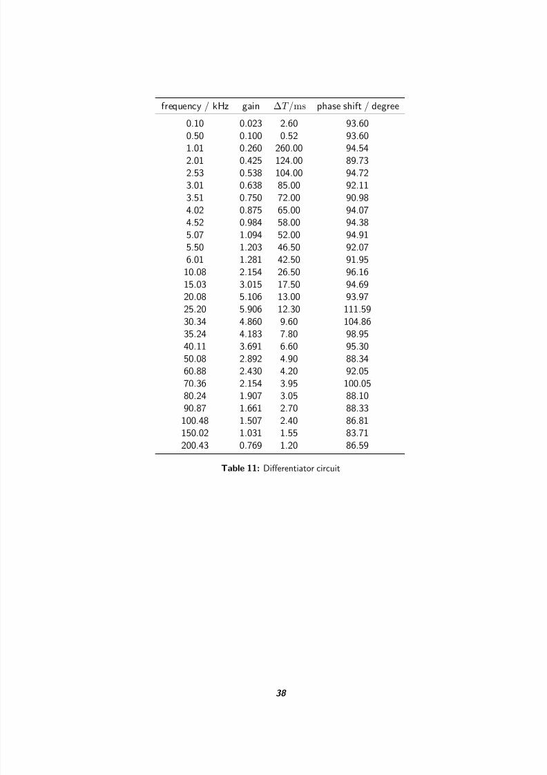
frequency / kHz gain ∆T /ms phase shift / degree
0.10 0.023 2.60 93.60
0.50 0.100 0.52 93.601.01 0.260 260.00 94.542.01 0.425 124.00 89.732.53 0.538 104.00 94.723.01 0.638 85.00 92.113.51 0.750 72.00 90.984.02 0.875 65.00 94.074.52 0.984 58.00 94.385.07 1.094 52.00 94.915.50 1.203 46.50 92.076.01 1.281 42.50 91.95
10.08 2.154 26.50 96.1615.03 3.015 17.50 94.6920.08 5.106 13.00 93.9725.20 5.906 12.30 111.5930.34 4.860 9.60 104.8635.24 4.183 7.80 98.9540.11 3.691 6.60 95.3050.08 2.892 4.90 88.3460.88 2.430 4.20 92.0570.36 2.154 3.95 100.0580.24 1.907 3.05 88.10
90.87 1.661 2.70 88.33100.48 1.507 2.40 86.81150.02 1.031 1.55 83.71200.43 0.769 1.20 86.59
Table 11: Differentiator circuit
38
8/4/2019 Analogue-electronics Laboratory Protocol
http://slidepdf.com/reader/full/analogue-electronics-laboratory-protocol 39/43
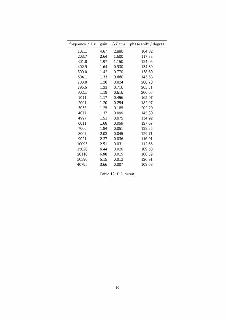
frequency / Hz gain ∆T /ms phase shift / degree
101.1 4.67 2.880 104.82
203.7 2.64 1.600 117.33301.8 1.97 1.150 124.95402.9 1.64 0.930 134.89500.0 1.42 0.770 138.60604.1 1.33 0.660 143.53703.8 1.26 0.824 208.78796.5 1.23 0.716 205.31902.1 1.18 0.616 200.051011 1.17 0.456 165.972001 1.20 0.254 182.973036 1.25 0.185 202.20
4077 1.37 0.099 145.304997 1.51 0.075 134.926011 1.68 0.059 127.677060 1.84 0.051 128.358007 2.03 0.045 129.719021 2.27 0.036 116.91
10095 2.51 0.031 112.6615020 6.44 0.020 109.5020110 6.98 0.015 108.5930390 5.15 0.012 126.9140795 3.66 0.007 108.68
Table 12: PID circuit
39
8/4/2019 Analogue-electronics Laboratory Protocol
http://slidepdf.com/reader/full/analogue-electronics-laboratory-protocol 40/43
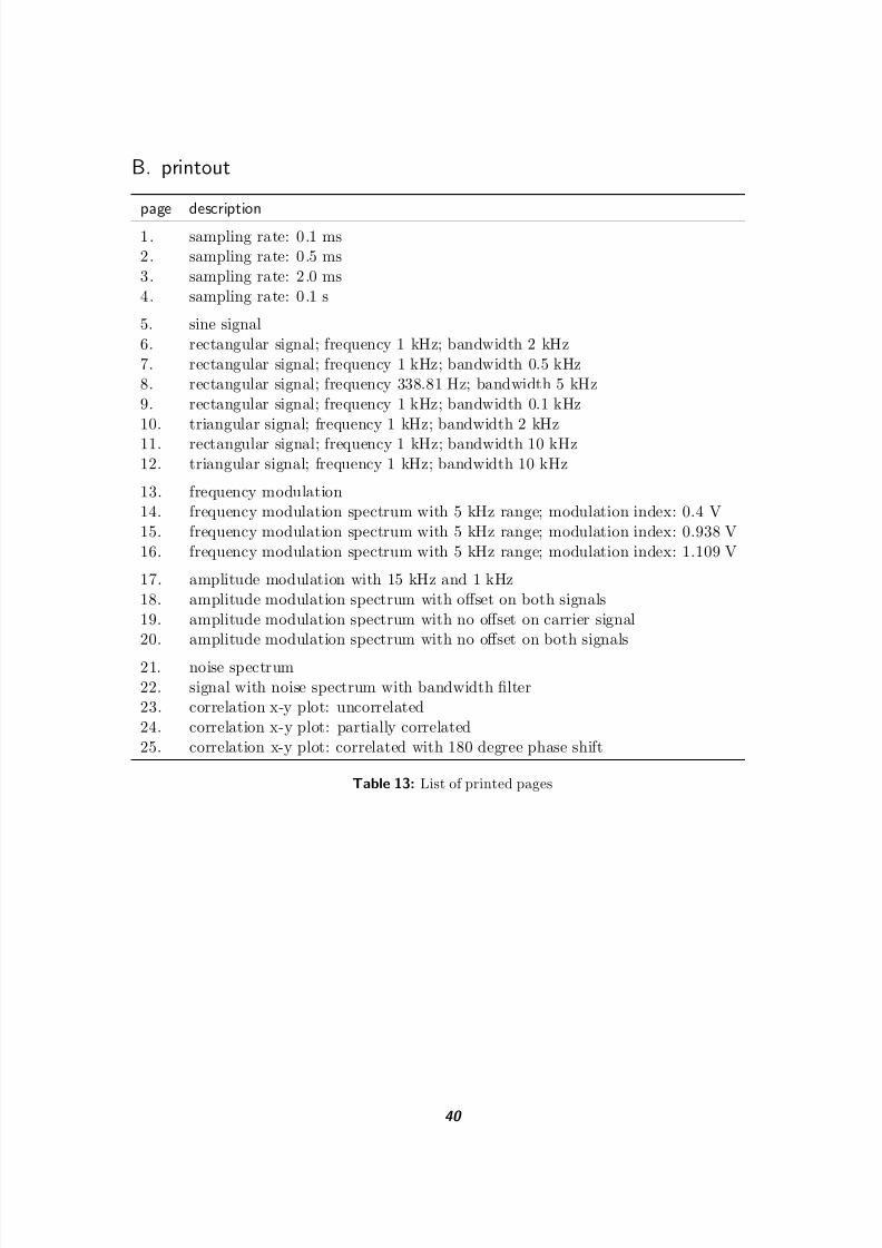
B. printout
page description
1. sampling rate: 0.1 ms2. sampling rate: 0.5 ms3. sampling rate: 2.0 ms4. sampling rate: 0.1 s
5. sine signal6. rectangular signal; frequency 1 kHz; bandwidth 2 kHz7. rectangular signal; frequency 1 kHz; bandwidth 0.5 kHz8. rectangular signal; frequency 338.81 Hz; bandwidth 5 kHz9. rectangular signal; frequency 1 kHz; bandwidth 0.1 kHz10. triangular signal; frequency 1 kHz; bandwidth 2 kHz
11. rectangular signal; frequency 1 kHz; bandwidth 10 kHz12. triangular signal; frequency 1 kHz; bandwidth 10 kHz
13. frequency modulation14. frequency modulation spectrum with 5 kHz range; modulation index: 0.4 V15. frequency modulation spectrum with 5 kHz range; modulation index: 0.938 V16. frequency modulation spectrum with 5 kHz range; modulation index: 1.109 V
17. amplitude modulation with 15 kHz and 1 kHz18. amplitude modulation spectrum with offset on both signals19. amplitude modulation spectrum with no offset on carrier signal20. amplitude modulation spectrum with no offset on both signals
21. noise spectrum22. signal with noise spectrum with bandwidth filter23. correlation x-y plot: uncorrelated24. correlation x-y plot: partially correlated25. correlation x-y plot: correlated with 180 degree phase shift
Table 13: List of printed pages
40
8/4/2019 Analogue-electronics Laboratory Protocol
http://slidepdf.com/reader/full/analogue-electronics-laboratory-protocol 41/43
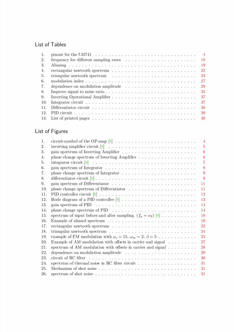
List of Tables
1. pinout for the LM741 . . . . . . . . . . . . . . . . . . . . . . . . . . . . . . . 4
2. frequency for different sampling rates . . . . . . . . . . . . . . . . . . . . . . 183. Aliasing . . . . . . . . . . . . . . . . . . . . . . . . . . . . . . . . . . . . . . . 194. rectangular sawtooth spectrum . . . . . . . . . . . . . . . . . . . . . . . . . . 225. triangular sawtooth spectrum . . . . . . . . . . . . . . . . . . . . . . . . . . 236. modulation index . . . . . . . . . . . . . . . . . . . . . . . . . . . . . . . . . . 277. dependence on modulation amplitude . . . . . . . . . . . . . . . . . . . . . . 298. Improve signal to noise ratio . . . . . . . . . . . . . . . . . . . . . . . . . . . . 359. Inverting Operational Amplifier . . . . . . . . . . . . . . . . . . . . . . . . . . 3710. Integrator circuit . . . . . . . . . . . . . . . . . . . . . . . . . . . . . . . . . . 3711. Differentiator circuit . . . . . . . . . . . . . . . . . . . . . . . . . . . . . . . . 3812. PID circuit . . . . . . . . . . . . . . . . . . . . . . . . . . . . . . . . . . . . . 39
13. List of printed pages . . . . . . . . . . . . . . . . . . . . . . . . . . . . . . . . 40
List of Figures
1. circuit-symbol of the OP-amp [8] . . . . . . . . . . . . . . . . . . . . . . . . . 42. inverting amplifier circuit [8] . . . . . . . . . . . . . . . . . . . . . . . . . . . 53. gain spectrum of Inverting Amplifier . . . . . . . . . . . . . . . . . . . . . . . 64. phase change spectrum of Inverting Amplifier . . . . . . . . . . . . . . . . . . 65. integrator circuit [8] . . . . . . . . . . . . . . . . . . . . . . . . . . . . . . . . 76. gain spectrum of Integrator . . . . . . . . . . . . . . . . . . . . . . . . . . . . 8
7. phase change spectrum of Integrator . . . . . . . . . . . . . . . . . . . . . . . 98. differentiator circuit [8] . . . . . . . . . . . . . . . . . . . . . . . . . . . . . . . 99. gain spectrum of Differentiator . . . . . . . . . . . . . . . . . . . . . . . . . . 1110. phase change spectrum of Differentiator . . . . . . . . . . . . . . . . . . . . . 1111. PID controller circuit [8] . . . . . . . . . . . . . . . . . . . . . . . . . . . . . . 1212. Bode diagram of a PID controller [8] . . . . . . . . . . . . . . . . . . . . . . . 1313. gain spectrum of PID . . . . . . . . . . . . . . . . . . . . . . . . . . . . . . . 1414. phase change spectrum of PID . . . . . . . . . . . . . . . . . . . . . . . . . . 1415. spectrum of input before and after sampling. (f a = ν S ) [8] . . . . . . . . . . . 1816. Example of aliased spectrum . . . . . . . . . . . . . . . . . . . . . . . . . . . 1917. rectangular sawtooth spectrum . . . . . . . . . . . . . . . . . . . . . . . . . . 22
18. triangular sawtooth spectrum . . . . . . . . . . . . . . . . . . . . . . . . . . . 2419. example of FM modulation with ωc = 15, ωm = 2, β = 5 . . . . . . . . . . . . 2520. Example of AM modulation with offsets in carrier and signal . . . . . . . . . 2721. spectrum of AM modulation with offsets in carrier and signal . . . . . . . . . 2822. dependence on modulation amplitude . . . . . . . . . . . . . . . . . . . . . . 2923. circuit of RC filter . . . . . . . . . . . . . . . . . . . . . . . . . . . . . . . . . 3024. spectrum of thermal noise in RC filter circuit . . . . . . . . . . . . . . . . . . 3125. Mechanism of shot noise . . . . . . . . . . . . . . . . . . . . . . . . . . . . . . 3126. spectrum of shot noise . . . . . . . . . . . . . . . . . . . . . . . . . . . . . . . 31
8/4/2019 Analogue-electronics Laboratory Protocol
http://slidepdf.com/reader/full/analogue-electronics-laboratory-protocol 42/43
27. spectrum of technical noise noise in RC filter circuit . . . . . . . . . . . . . . 3228. spectrum of generation and recombination noise . . . . . . . . . . . . . . . . 3229. spectrum of white noise . . . . . . . . . . . . . . . . . . . . . . . . . . . . . . 3330. Bandpass filter circuit . . . . . . . . . . . . . . . . . . . . . . . . . . . . . . . 3331. Bandpass characteristic . . . . . . . . . . . . . . . . . . . . . . . . . . . . . . 3432. Signal to noise ratio . . . . . . . . . . . . . . . . . . . . . . . . . . . . . . . . 35
8/4/2019 Analogue-electronics Laboratory Protocol
http://slidepdf.com/reader/full/analogue-electronics-laboratory-protocol 43/43
References
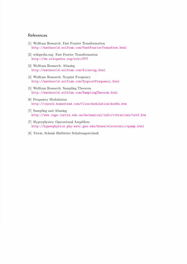
[1] Wolfram Research: Fast Fourier Transformationhttp://mathworld.wolfram.com/FastFourierTransform.html
[2] wikipedia.org: Fast Fourier Transformationhttp://de.wikipedia.org/wiki/FFT
[3] Wolfram Research: Aliasing
http://mathworld.wolfram.com/Aliasing.html
[4] Wolfram Research: Nyquist Frequencyhttp://mathworld.wolfram.com/NyquistFrequency.html
[5] Wolfram Research: Sampling Theorem
http://mathworld.wolfram.com/SamplingTheorem.html
[6] Frequency Modulationhttp://cnyack.homestead.com/files/modulation/modfm.htm
[7] Sampling and Aliasing
http://www.cage.curtin.edu.au/mechanical/info/vibrations/tut3.htm
[7] Hyperphysics: Operational Amplifiers
http://hyperphysics.phy-astr.gsu.edu/hbase/electronic/opamp.html
[8] Tietze, Schenk Halbleiter Schaltungstechnik


![ANALOGUE AND DIGITAL ELECTRONICS TEACHING NOTES U2: … · 2014. 8. 6. · Electronics 2-Analogue electronics. 4 [ b] Current through a resistor equals the voltage across it divided](https://img.pdfslide.net/doc/110x75/5febd5cc6354ef645c429594/analogue-and-digital-electronics-teaching-notes-u2-2014-8-6-electronics-2-analogue.jpg)