Embed Size (px)
Citation preview
NANO REVIEW Open Access
Atom devices based on single dopants in siliconnanostructuresDaniel Moraru1, Arief Udhiarto1, Miftahul Anwar1, Roland Nowak1,2, Ryszard Jablonski2, Earfan Hamid1,Juli Cha Tarido1, Takeshi Mizuno1 and Michiharu Tabe1*
Abstract
Silicon field-effect transistors have now reached gate lengths of only a few tens of nanometers, containing acountable number of dopants in the channel. Such technological trend brought us to a research stage on devicesworking with one or a few dopant atoms. In this work, we review our most recent studies on key atom deviceswith fundamental structures of silicon-on-insulator MOSFETs, such as single-dopant transistors, preliminary memorydevices, single-electron turnstile devices and photonic devices, in which electron tunneling mediated by singledopant atoms is the essential transport mechanism. Furthermore, observation of individual dopant potential in thechannel by Kelvin probe force microscopy is also presented. These results may pave the way for the developmentof a new device technology, i.e., single-dopant atom electronics.
Keywords: single-dopant electronics, single-electron tunneling, double-donor systems, multiple-donor systems,photon, Kelvin probe force microscopy, silicon-on-insulator field-effect transistor
IntroductionAfter demonstration of the first semiconductor transis-tor, it was soon realized that semiconductors requiredoping with impurity atoms for achieving useful func-tionalities [1,2]. Dopants have played a key role in thefast-paced development of the electronics industry,dominantly based on silicon. As predicted by Moore’slaw in the 1960s [3], silicon transistors were expected togo through a miniaturization process, and this trend hasbeen pursued for nearly half a century now. The transis-tor’s gate length is now only several tens of nanometers,and it will be further downscaled to the 22-nm nodeand beyond [4]. This miniaturization faces many techno-logical and fundamental challenges, among which a keyproblem is the discrete dopant distribution in the devicechannel [5]. Each individual dopant, having basically anuncontrolled position in the channel, significantly affectsdevice characteristics [5,6], leading to device-to-devicevariability. It was shown that controlled positioning ofdopants by single-ion implantation in the device channel
can reduce threshold voltage variability in metal-oxide-semiconductor field-effect transistors (MOSFETs) [7].On the other hand, technological progress offers a
unique opportunity, i.e., electrical access to individualdopant atoms in nanometer-scale devices. Properties ofdopant atoms that have been so far inferred from mea-surements of bulk materials, containing a large numberof dopants, can now be associated to a specific dopantatom through direct measurements.Recently, breakthrough results indicate the possibility
of individually addressing dopants in silicon, as illu-strated in Figure 1. When the dopant is located in ananoscale-channel field-effect transistor (FET), single-electron tunneling via the dopant-induced quantum dot(QD) gives rise to measurable currents. Results illustrat-ing this operation mode have been obtained at cryogenicor low temperature in transistors containing in theirchannel one or only a few dopant atoms. Single-electrontunneling spectroscopy of arsenic (As) donors, locatedin the edges of FinFET channels, was performed at cryo-genic temperatures [8-10]. Acceptors, such as boron (B),were also directly identified in low-temperature trans-port characteristics of silicon-on-insulator (SOI) FETs[11,12]. Individual dopants can be accessed even indopant-rich environments, where the channel contains
* Correspondence: [email protected] Institute of Electronics, Shizuoka University, 3-5-1 Johoku, Nakaku,Hamamatsu, 432-8011, JapanFull list of author information is available at the end of the article
Moraru et al. Nanoscale Research Letters 2011, 6:479http://www.nanoscalereslett.com/content/6/1/479
© 2011 Moraru et al; licensee Springer. This is an Open Access article distributed under the terms of the Creative Commons AttributionLicense (http://creativecommons.org/licenses/by/2.0), which permits unrestricted use, distribution, and reproduction in any medium,provided the original work is properly cited.
more than only one isolated dopant atom [13]. In orderto observe individual donor and/or acceptor impurities,scanning probe techniques are typically used, amongwhich Kelvin probe force microscopy (KFM) allowedmapping of dopants in channels of Si nanodevices undernormal operation conditions [14,15].These findings accelerated research on individual
dopant atoms in silicon nanostructures, as well as oninteractions between dopants and the surroundingenvironment. Donor interface coupling has been inten-sively studied mostly from a theoretical approach[16-18], mainly for quantum computing [19,20], whichinvolves transfer of an electron between a donor and anearby interface. Furthermore, it has been predicted thatdopant properties are significantly different in nanos-tructures due to effects such as dielectric confinementand quantum confinement [21]. It was found that theactivation energy of dopants is enhanced in nanostruc-tures, leading to reduced doping efficiency in doped Sinanowires [22]. This opens, however, an additionalopportunity in terms of physics, since it may be possibleto tune the properties of dopants by a suitable design ofthe nanoscale environment.These developments justify an increasing interest in
studies of single dopants in nanoscale Si transistors.Such studies may eventually enable us to develop anentire field of electronics, single-dopant electronics, inwhich the basic operation mode will be single-electrontunneling mediated by an individual dopant.In this paper, we outline some of our recent results,
focused on isolating single dopant features in electricalcharacteristics of nanoscale phosphorus-doped channel
SOI-FETs. First, we will show that single dopants can beelectrically addressed even in devices that contain morethan just one isolated dopant in the channel [13]. Formore advanced device functions, coupling between dis-crete dopants is expected to play a key role. Systems inwhich we identified two coupled donors dominating thecharacteristics will be described [23]. We will alsoaddress other application possibilities, such as single-electron turnstiles, that can be conceived using morecomplex donor arrays [24-27]. Additional functionalitiescan be expected when photons are incorporated indevice operation [28]; as a first step, we will showresults that indicate trapping of single photon-generatedelectrons by individual donors in an FET channel. Directobservation of dopant potentials in device channelsusing a Kelvin probe force microscopy technique[14,15,29] will also be presented. An overview of possi-ble research directions in the field of single-dopant elec-tronics will be given before the summary.
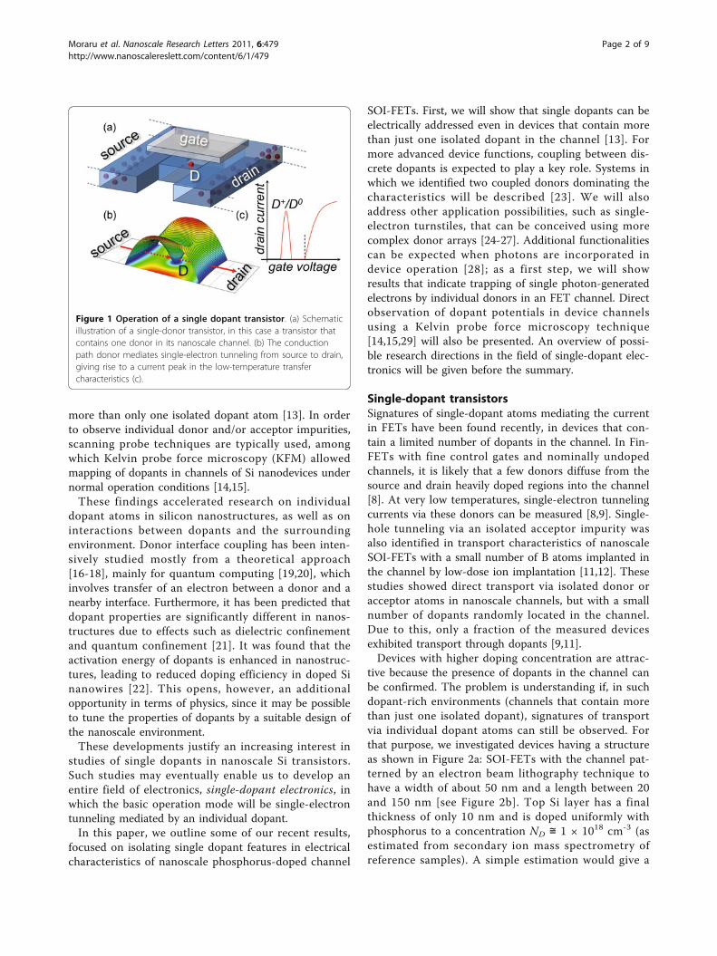
Single-dopant transistorsSignatures of single-dopant atoms mediating the currentin FETs have been found recently, in devices that con-tain a limited number of dopants in the channel. In Fin-FETs with fine control gates and nominally undopedchannels, it is likely that a few donors diffuse from thesource and drain heavily doped regions into the channel[8]. At very low temperatures, single-electron tunnelingcurrents via these donors can be measured [8,9]. Single-hole tunneling via an isolated acceptor impurity wasalso identified in transport characteristics of nanoscaleSOI-FETs with a small number of B atoms implanted inthe channel by low-dose ion implantation [11,12]. Thesestudies showed direct transport via isolated donor oracceptor atoms in nanoscale channels, but with a smallnumber of dopants randomly located in the channel.Due to this, only a fraction of the measured devicesexhibited transport through dopants [9,11].Devices with higher doping concentration are attrac-
tive because the presence of dopants in the channel canbe confirmed. The problem is understanding if, in suchdopant-rich environments (channels that contain morethan just one isolated dopant), signatures of transportvia individual dopant atoms can still be observed. Forthat purpose, we investigated devices having a structureas shown in Figure 2a: SOI-FETs with the channel pat-terned by an electron beam lithography technique tohave a width of about 50 nm and a length between 20and 150 nm [see Figure 2b]. Top Si layer has a finalthickness of only 10 nm and is doped uniformly withphosphorus to a concentration ND ≅ 1 × 1018 cm-3 (asestimated from secondary ion mass spectrometry ofreference samples). A simple estimation would give a
Figure 1 Operation of a single dopant transistor. (a) Schematicillustration of a single-donor transistor, in this case a transistor thatcontains one donor in its nanoscale channel. (b) The conductionpath donor mediates single-electron tunneling from source to drain,giving rise to a current peak in the low-temperature transfercharacteristics (c).
Moraru et al. Nanoscale Research Letters 2011, 6:479http://www.nanoscalereslett.com/content/6/1/479
Page 2 of 9
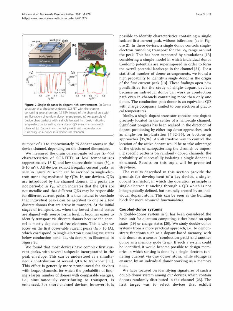
number of 10 to approximately 75 dopant atoms in thedevice channel, depending on the channel dimensions.We measured the drain current-gate voltage (ID-VG)
characteristics of SOI-FETs at low temperatures(approximately 15 K) and low source-drain biases (VD =5-10 mV). All devices exhibit irregular current peaks, asseen in Figure 2c, which can be ascribed to single-elec-tron tunneling mediated by QDs. In our devices, QDsare introduced by the channel donors. The peaks arenot periodic in VG, which indicates that the QDs arenot metallic and that different QDs may be responsiblefor different current peaks. It is thus natural to concludethat individual peaks can be ascribed to one or a fewdiscrete donors that are active in transport. At the initialstages of transport, i.e., when the lowest channel statesare aligned with source Fermi level, it becomes easier toidentify transport via discrete donors because the chan-nel is mostly depleted of free electrons. This is why wefocus on the first observable current peaks (ID > 10 fA),which correspond to single-electron tunneling via statesbelow conduction band, i.e., via donors, as illustrated inFigure 2d.We found that most devices have complex first cur-
rent peaks, with several subpeaks incorporated in thepeak envelope. This can be understood as a simulta-neous contribution of several QDs to transport [30].This effect is generally more pronounced for deviceswith longer channels, for which the probability of find-ing a larger number of donors with comparable energies,i.e., simultaneously contributing to transport, isenhanced. For short-channel devices, however, it is
possible to identify characteristics containing a singleisolated first current peak, without inflections (as in Fig-ure 2). In these devices, a single donor controls single-electron tunneling transport for the VG range aroundthe peak. This has been supported by simulations [13]considering a simple model in which individual donorCoulomb potentials are superimposed in order to formthe overall potential landscape in the channel [31]. For astatistical number of donor arrangements, we found ahigh probability to identify a single donor as the originof the first current peak [13]. These findings open newpossibilities for the study of single-dopant devicesbecause an individual donor can work as conductionpath even in channels containing more than only onedonor. The conduction path donor is an equivalent QDwith charge occupancy limited to one electron at practi-cal temperatures.Ideally, a single-dopant transistor contains one dopant
precisely located in the center of a nanoscale channel.Significant progress has been realized in the direction ofdopant positioning by either top-down approaches, suchas single-ion implantation [7,32-34], or bottom-upapproaches [35,36]. An alternative way to control thelocation of the active dopant would be to take advantageof the effects of nanopatterning the channel; by impos-ing specific patterns on randomly doped channels, theprobability of successfully isolating a single dopant isenhanced. Results on this topic will be presentedelsewhere.The results described in this section provide the
grounds for development of a key device, a single-dopant transistor, in which the operation principle issingle-electron tunneling through a QD which is notlithographically defined, but naturally created by an indi-vidual dopant atom. This can be seen as the buildingblock for more advanced functionalities.
Coupled-donor systemsA double-donor system in Si has been considered thebasic unit for quantum computing, either based on spinstates [19] or charge states [20]. We study double-donorsystems from a more practical approach, i.e., to demon-strate functions such as a dopant-based memory, withone donor as a sensor (conduction path) and anotherdonor as a memory node (trap). If such a system couldbe identified, it would become possible to design mem-ories in which sensing is done by a single-electron tun-neling current via one donor atom, while storage isensured by an individual donor working as a memorynode.We have focused on identifying signatures of such a
double-donor system among our devices, which containdonors randomly distributed in the channel [23]. Thefirst target was to select devices that exhibit
Figure 2 Single dopants in dopant-rich environment. (a) Devicestructure of a phosphorus-doped SOI-FET with the channelcontaining several donors. (b) SEM image of the channel area withan illustration of random donor arrangement. (c) An example ofdevice characteristics with a single isolated first peak, indicatingsingle-electron tunneling via a donor QD even in a donor-richchannel. (d) Zoom in on the first peak (inset: single-electrontunneling via a donor in a donor-rich channel).
Moraru et al. Nanoscale Research Letters 2011, 6:479http://www.nanoscalereslett.com/content/6/1/479
Page 3 of 9
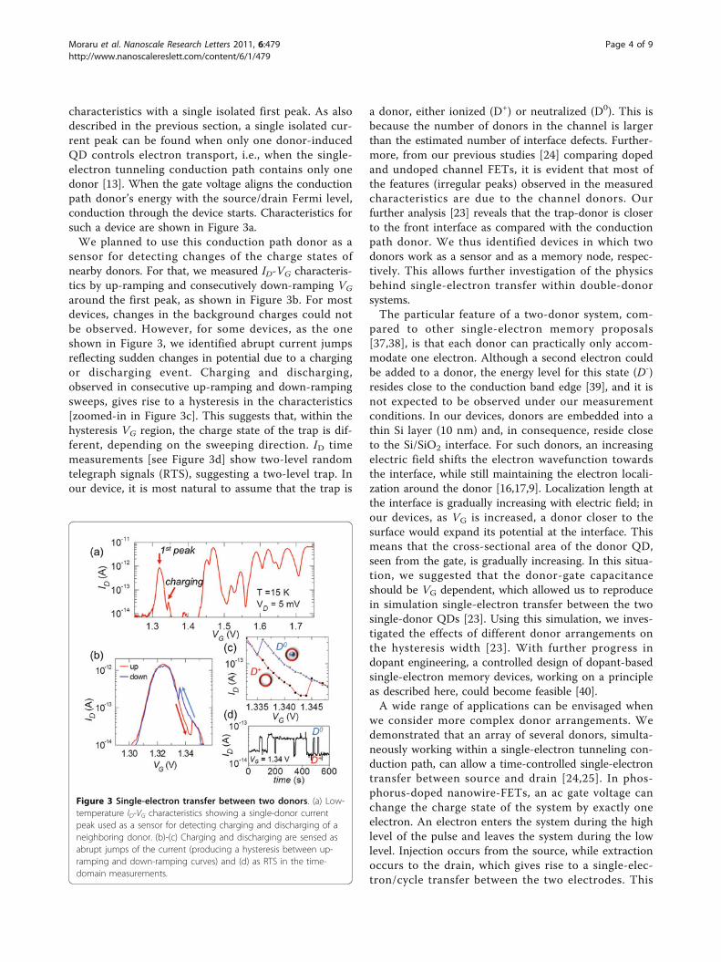
characteristics with a single isolated first peak. As alsodescribed in the previous section, a single isolated cur-rent peak can be found when only one donor-inducedQD controls electron transport, i.e., when the single-electron tunneling conduction path contains only onedonor [13]. When the gate voltage aligns the conductionpath donor’s energy with the source/drain Fermi level,conduction through the device starts. Characteristics forsuch a device are shown in Figure 3a.We planned to use this conduction path donor as a
sensor for detecting changes of the charge states ofnearby donors. For that, we measured ID-VG characteris-tics by up-ramping and consecutively down-ramping VG
around the first peak, as shown in Figure 3b. For mostdevices, changes in the background charges could notbe observed. However, for some devices, as the oneshown in Figure 3, we identified abrupt current jumpsreflecting sudden changes in potential due to a chargingor discharging event. Charging and discharging,observed in consecutive up-ramping and down-rampingsweeps, gives rise to a hysteresis in the characteristics[zoomed-in in Figure 3c]. This suggests that, within thehysteresis VG region, the charge state of the trap is dif-ferent, depending on the sweeping direction. ID timemeasurements [see Figure 3d] show two-level randomtelegraph signals (RTS), suggesting a two-level trap. Inour device, it is most natural to assume that the trap is
a donor, either ionized (D+) or neutralized (D0). This isbecause the number of donors in the channel is largerthan the estimated number of interface defects. Further-more, from our previous studies [24] comparing dopedand undoped channel FETs, it is evident that most ofthe features (irregular peaks) observed in the measuredcharacteristics are due to the channel donors. Ourfurther analysis [23] reveals that the trap-donor is closerto the front interface as compared with the conductionpath donor. We thus identified devices in which twodonors work as a sensor and as a memory node, respec-tively. This allows further investigation of the physicsbehind single-electron transfer within double-donorsystems.The particular feature of a two-donor system, com-
pared to other single-electron memory proposals[37,38], is that each donor can practically only accom-modate one electron. Although a second electron couldbe added to a donor, the energy level for this state (D-)resides close to the conduction band edge [39], and it isnot expected to be observed under our measurementconditions. In our devices, donors are embedded into athin Si layer (10 nm) and, in consequence, reside closeto the Si/SiO2 interface. For such donors, an increasingelectric field shifts the electron wavefunction towardsthe interface, while still maintaining the electron locali-zation around the donor [16,17,9]. Localization length atthe interface is gradually increasing with electric field; inour devices, as VG is increased, a donor closer to thesurface would expand its potential at the interface. Thismeans that the cross-sectional area of the donor QD,seen from the gate, is gradually increasing. In this situa-tion, we suggested that the donor-gate capacitanceshould be VG dependent, which allowed us to reproducein simulation single-electron transfer between the twosingle-donor QDs [23]. Using this simulation, we inves-tigated the effects of different donor arrangements onthe hysteresis width [23]. With further progress indopant engineering, a controlled design of dopant-basedsingle-electron memory devices, working on a principleas described here, could become feasible [40].A wide range of applications can be envisaged when
we consider more complex donor arrangements. Wedemonstrated that an array of several donors, simulta-neously working within a single-electron tunneling con-duction path, can allow a time-controlled single-electrontransfer between source and drain [24,25]. In phos-phorus-doped nanowire-FETs, an ac gate voltage canchange the charge state of the system by exactly oneelectron. An electron enters the system during the highlevel of the pulse and leaves the system during the lowlevel. Injection occurs from the source, while extractionoccurs to the drain, which gives rise to a single-elec-tron/cycle transfer between the two electrodes. This
Figure 3 Single-electron transfer between two donors. (a) Low-temperature ID-VG characteristics showing a single-donor currentpeak used as a sensor for detecting charging and discharging of aneighboring donor. (b)-(c) Charging and discharging are sensed asabrupt jumps of the current (producing a hysteresis between up-ramping and down-ramping curves) and (d) as RTS in the time-domain measurements.
Moraru et al. Nanoscale Research Letters 2011, 6:479http://www.nanoscalereslett.com/content/6/1/479
Page 4 of 9
operation is similar to single-electron turnstile devicesproposed with metallic QDs [41] or with semiconductorQDs [42,43], with the key difference that in our devicesQDs are dopant atoms. From simulation studies [26,27],we found that the natural inhomogeneity of device para-meters (mainly donor-gate capacitances) plays an impor-tant role in single-electron turnstile operation.In short, various applications can be designed using
charge states of coupled donors, suggesting that there isa rich environment for further research and develop-ment of functionalities downscaled to the level of dis-crete donors.
Photon effects in doped channel FETsFunctionalities presented so far rely on single-electrontunneling via one donor or coupled donors in dark con-ditions, i.e., without photon illumination. However, therange of applications for donor-based systems can bedrastically enhanced by purposely incorporating photoneffects. Based on the interaction between photons anddopants, dopant-based optoelectronic devices could bedeveloped.The effects of photon illumination on semiconductor
devices have been studied for a long time, mainly fordeveloping high-speed photodetectors [44] or solar cells[45]. For FET devices, when photons are irradiated onthe channel, a fraction of incident photons will beabsorbed in the device active region. By absorption of aphoton, an electron-hole pair is generated, and carriersmay either contribute to conduction, recombine witheach other, or become trapped in available traps. Signifi-cant research has been done on demonstrating trappingof photo-generated carriers in QDs [46,47]. It was foundthat QD arrays may work as a building block for single-photon detection, involving trapping of elementarycharges in a QD and sensing it with a current flowingas a percolation path in the channel. Such devices havelow quantum detection efficiencies, but demonstratethat single photons can play an active role in the trap-ping of single carriers.A similar mechanism could be expected when the QD
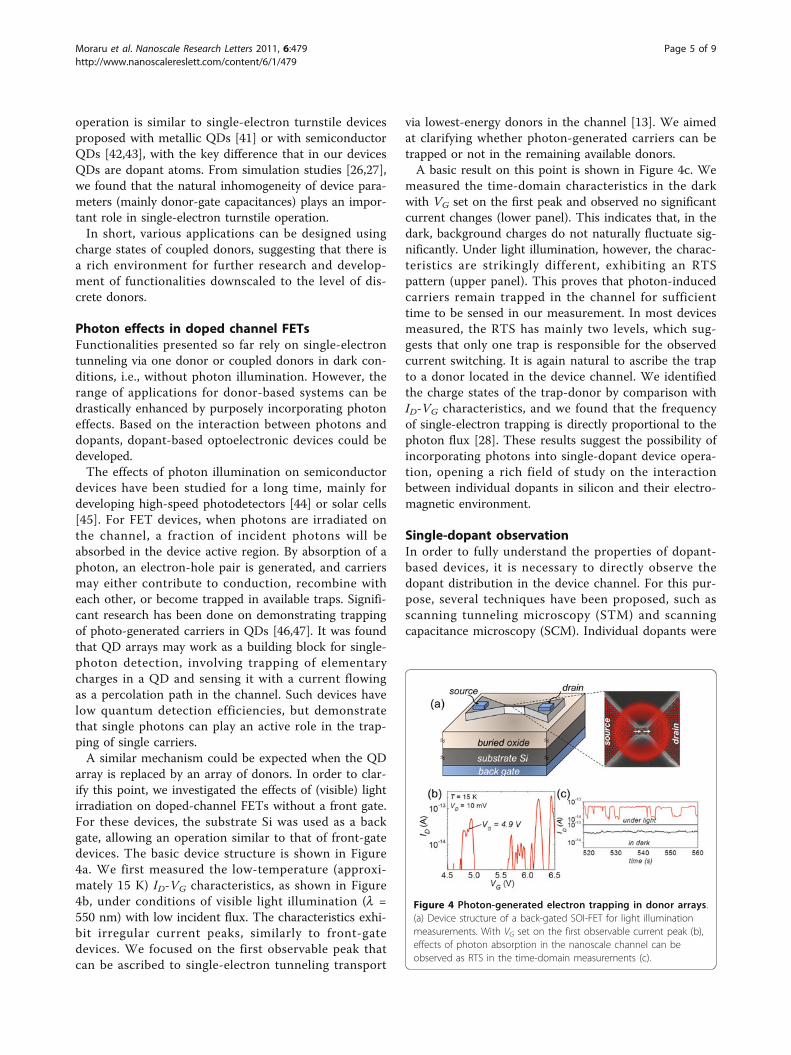
array is replaced by an array of donors. In order to clar-ify this point, we investigated the effects of (visible) lightirradiation on doped-channel FETs without a front gate.For these devices, the substrate Si was used as a backgate, allowing an operation similar to that of front-gatedevices. The basic device structure is shown in Figure4a. We first measured the low-temperature (approxi-mately 15 K) ID-VG characteristics, as shown in Figure4b, under conditions of visible light illumination (l =550 nm) with low incident flux. The characteristics exhi-bit irregular current peaks, similarly to front-gatedevices. We focused on the first observable peak thatcan be ascribed to single-electron tunneling transport
via lowest-energy donors in the channel [13]. We aimedat clarifying whether photon-generated carriers can betrapped or not in the remaining available donors.A basic result on this point is shown in Figure 4c. We
measured the time-domain characteristics in the darkwith VG set on the first peak and observed no significantcurrent changes (lower panel). This indicates that, in thedark, background charges do not naturally fluctuate sig-nificantly. Under light illumination, however, the charac-teristics are strikingly different, exhibiting an RTSpattern (upper panel). This proves that photon-inducedcarriers remain trapped in the channel for sufficienttime to be sensed in our measurement. In most devicesmeasured, the RTS has mainly two levels, which sug-gests that only one trap is responsible for the observedcurrent switching. It is again natural to ascribe the trapto a donor located in the device channel. We identifiedthe charge states of the trap-donor by comparison withID-VG characteristics, and we found that the frequencyof single-electron trapping is directly proportional to thephoton flux [28]. These results suggest the possibility ofincorporating photons into single-dopant device opera-tion, opening a rich field of study on the interactionbetween individual dopants in silicon and their electro-magnetic environment.
Single-dopant observationIn order to fully understand the properties of dopant-based devices, it is necessary to directly observe thedopant distribution in the device channel. For this pur-pose, several techniques have been proposed, such asscanning tunneling microscopy (STM) and scanningcapacitance microscopy (SCM). Individual dopants were
Figure 4 Photon-generated electron trapping in donor arrays.(a) Device structure of a back-gated SOI-FET for light illuminationmeasurements. With VG set on the first observable current peak (b),effects of photon absorption in the nanoscale channel can beobserved as RTS in the time-domain measurements (c).
Moraru et al. Nanoscale Research Letters 2011, 6:479http://www.nanoscalereslett.com/content/6/1/479
Page 5 of 9
successfully observed using STM techniques on sampleswith a specific surface treatment [35,48,49]. STM, how-ever, relies on measuring tunneling currents between ametallic tip and the sample, and it can only detect pointcharges located in the topmost few layers. SCM is basedon evaluating the capacitance between a tip and thesample, allowing for subsequent extraction of dopantprofiles [50,51]. This technique is, however, limited bythe tip and sample quality, which strongly affect themeasured capacitance values.The main issue with mapping dopants in FET chan-
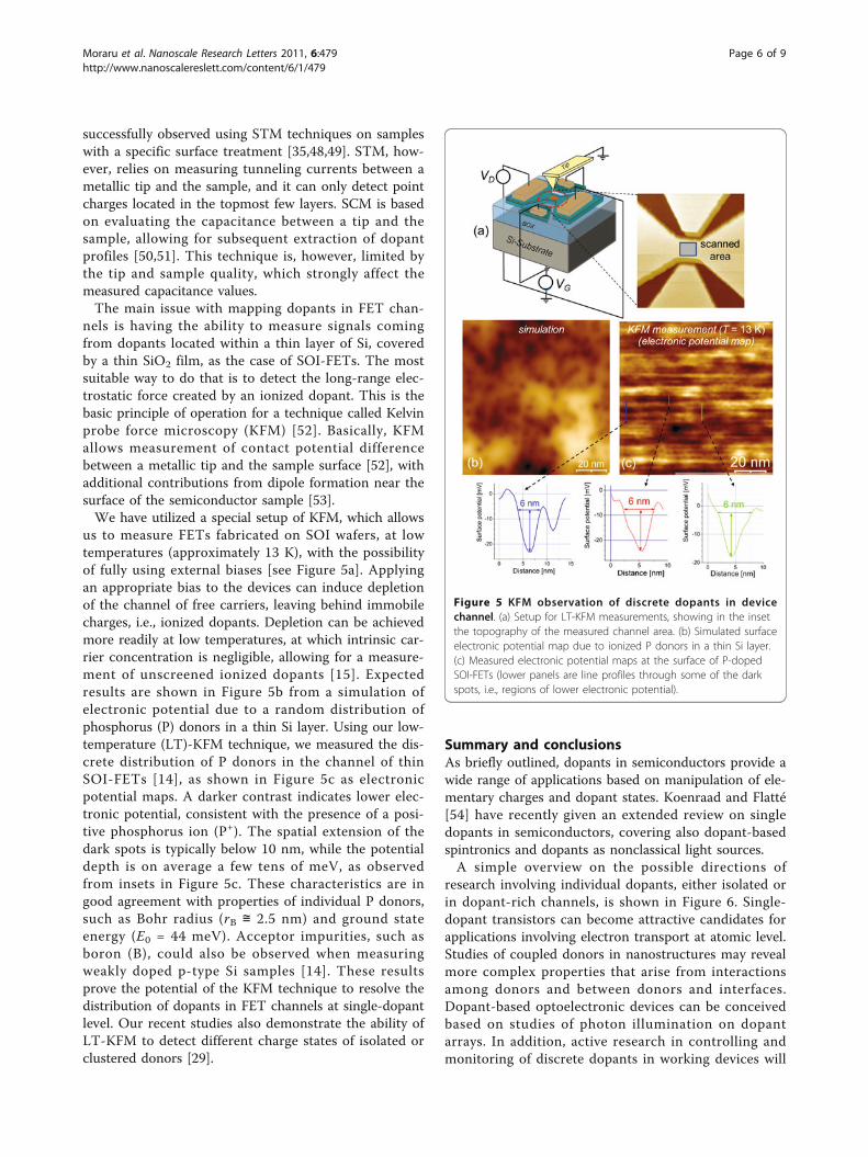
nels is having the ability to measure signals comingfrom dopants located within a thin layer of Si, coveredby a thin SiO2 film, as the case of SOI-FETs. The mostsuitable way to do that is to detect the long-range elec-trostatic force created by an ionized dopant. This is thebasic principle of operation for a technique called Kelvinprobe force microscopy (KFM) [52]. Basically, KFMallows measurement of contact potential differencebetween a metallic tip and the sample surface [52], withadditional contributions from dipole formation near thesurface of the semiconductor sample [53].We have utilized a special setup of KFM, which allows
us to measure FETs fabricated on SOI wafers, at lowtemperatures (approximately 13 K), with the possibilityof fully using external biases [see Figure 5a]. Applyingan appropriate bias to the devices can induce depletionof the channel of free carriers, leaving behind immobilecharges, i.e., ionized dopants. Depletion can be achievedmore readily at low temperatures, at which intrinsic car-rier concentration is negligible, allowing for a measure-ment of unscreened ionized dopants [15]. Expectedresults are shown in Figure 5b from a simulation ofelectronic potential due to a random distribution ofphosphorus (P) donors in a thin Si layer. Using our low-temperature (LT)-KFM technique, we measured the dis-crete distribution of P donors in the channel of thinSOI-FETs [14], as shown in Figure 5c as electronicpotential maps. A darker contrast indicates lower elec-tronic potential, consistent with the presence of a posi-tive phosphorus ion (P+). The spatial extension of thedark spots is typically below 10 nm, while the potentialdepth is on average a few tens of meV, as observedfrom insets in Figure 5c. These characteristics are ingood agreement with properties of individual P donors,such as Bohr radius (rB ≅ 2.5 nm) and ground stateenergy (E0 = 44 meV). Acceptor impurities, such asboron (B), could also be observed when measuringweakly doped p-type Si samples [14]. These resultsprove the potential of the KFM technique to resolve thedistribution of dopants in FET channels at single-dopantlevel. Our recent studies also demonstrate the ability ofLT-KFM to detect different charge states of isolated orclustered donors [29].
Summary and conclusionsAs briefly outlined, dopants in semiconductors provide awide range of applications based on manipulation of ele-mentary charges and dopant states. Koenraad and Flatté[54] have recently given an extended review on singledopants in semiconductors, covering also dopant-basedspintronics and dopants as nonclassical light sources.A simple overview on the possible directions of
research involving individual dopants, either isolated orin dopant-rich channels, is shown in Figure 6. Single-dopant transistors can become attractive candidates forapplications involving electron transport at atomic level.Studies of coupled donors in nanostructures may revealmore complex properties that arise from interactionsamong donors and between donors and interfaces.Dopant-based optoelectronic devices can be conceivedbased on studies of photon illumination on dopantarrays. In addition, active research in controlling andmonitoring of discrete dopants in working devices will
Figure 5 KFM observation of discrete dopants in devicechannel. (a) Setup for LT-KFM measurements, showing in the insetthe topography of the measured channel area. (b) Simulated surfaceelectronic potential map due to ionized P donors in a thin Si layer.(c) Measured electronic potential maps at the surface of P-dopedSOI-FETs (lower panels are line profiles through some of the darkspots, i.e., regions of lower electronic potential).
Moraru et al. Nanoscale Research Letters 2011, 6:479http://www.nanoscalereslett.com/content/6/1/479
Page 6 of 9
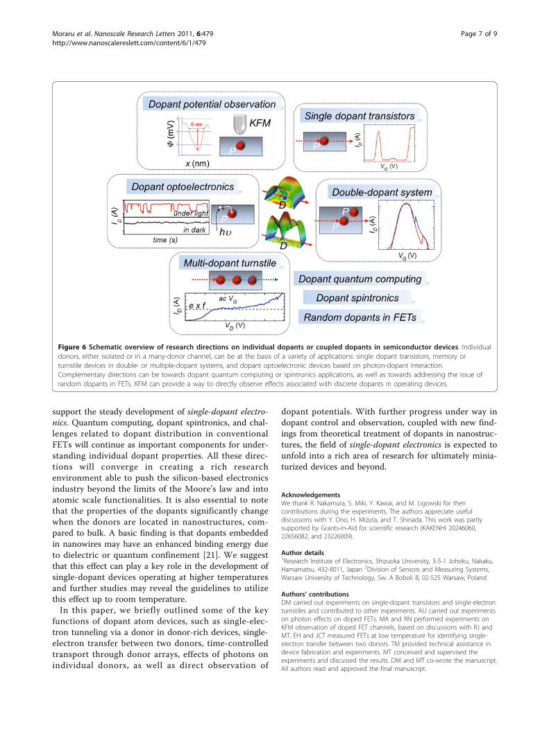
support the steady development of single-dopant electro-nics. Quantum computing, dopant spintronics, and chal-lenges related to dopant distribution in conventionalFETs will continue as important components for under-standing individual dopant properties. All these direc-tions will converge in creating a rich researchenvironment able to push the silicon-based electronicsindustry beyond the limits of the Moore’s law and intoatomic scale functionalities. It is also essential to notethat the properties of the dopants significantly changewhen the donors are located in nanostructures, com-pared to bulk. A basic finding is that dopants embeddedin nanowires may have an enhanced binding energy dueto dielectric or quantum confinement [21]. We suggestthat this effect can play a key role in the development ofsingle-dopant devices operating at higher temperaturesand further studies may reveal the guidelines to utilizethis effect up to room temperature.In this paper, we briefly outlined some of the key
functions of dopant atom devices, such as single-elec-tron tunneling via a donor in donor-rich devices, single-electron transfer between two donors, time-controlledtransport through donor arrays, effects of photons onindividual donors, as well as direct observation of
dopant potentials. With further progress under way indopant control and observation, coupled with new find-ings from theoretical treatment of dopants in nanostruc-tures, the field of single-dopant electronics is expected tounfold into a rich area of research for ultimately minia-turized devices and beyond.
AcknowledgementsWe thank R. Nakamura, S. Miki, Y. Kawai, and M. Ligowski for theircontributions during the experiments. The authors appreciate usefuldiscussions with Y. Ono, H. Mizuta, and T. Shinada. This work was partlysupported by Grants-in-Aid for scientific research (KAKENHI 20246060,22656082, and 23226009).
Author details1Research Institute of Electronics, Shizuoka University, 3-5-1 Johoku, Nakaku,Hamamatsu, 432-8011, Japan 2Division of Sensors and Measuring Systems,Warsaw University of Technology, Sw. A Boboli 8, 02-525 Warsaw, Poland
Authors’ contributionsDM carried out experiments on single-dopant transistors and single-electronturnstiles and contributed to other experiments. AU carried out experimentson photon effects on doped FETs. MA and RN performed experiments onKFM observation of doped FET channels, based on discussions with RJ andMT. EH and JCT measured FETs at low temperature for identifying single-electron transfer between two donors. TM provided technical assistance indevice fabrication and experiments. MT conceived and supervised theexperiments and discussed the results. DM and MT co-wrote the manuscript.All authors read and approved the final manuscript.
Figure 6 Schematic overview of research directions on individual dopants or coupled dopants in semiconductor devices. Individualdonors, either isolated or in a many-donor channel, can be at the basis of a variety of applications: single dopant transistors, memory orturnstile devices in double- or multiple-dopant systems, and dopant optoelectronic devices based on photon-dopant interaction.Complementary directions can be towards dopant quantum computing or spintronics applications, as well as towards addressing the issue ofrandom dopants in FETs. KFM can provide a way to directly observe effects associated with discrete dopants in operating devices.
Moraru et al. Nanoscale Research Letters 2011, 6:479http://www.nanoscalereslett.com/content/6/1/479
Page 7 of 9
Competing interestsThe authors declare that they have no competing interests.
Received: 11 May 2011 Accepted: 29 July 2011 Published: 29 July 2011
References1. Pearson GL, Bardeen J: Electrical properties of pure silicon and silicon
alloys containing boron and phosphorus. Phys Rev 1949, 75:865-883.2. Kohn W, Luttinger JM: Theory of donor states in silicon. Phys Rev 1955,
98:915-922.3. Moore G: Cramming more components onto integrated circuits.
Electronics 1965, 38:114-117.4. International Technology Roadmap for Semiconductors. [http://www.itrs.
net/].5. Asenov A: Random dopant induced threshold voltage lowering and
fluctuations in sub-0.1 μm MOSFETs: a 3-D “atomistic” simulation study.IEEE Trans Electron Devices 1998, 45:2505-2513.
6. Pierre M, Wacquez R, Jehl X, Sanquer M, Vinet M, Cueto O: Single-donorionization energies in a nanoscale CMOS channel. Nat Nanotechnol 2010,5:133-137.
7. Shinada T, Okamoto S, Kobayashi T, Ohdomari I: Enhancing semiconductordevice performance using ordered dopant arrays. Nature 2005,437:1128-1131.
8. Sellier H, Lansbergen GP, Caro J, Rogge S, Collaert N, Ferain I, Jurczak M,Biesemans S: Transport spectroscopy of a single dopant in a gatedsilicon nanowire. Phys Rev Lett 2006, 97:206805.
9. Lansbergen GP, Rahman R, Wellard CJ, Woo I, Caro J, Collaert N,Biesemans S, Klimeck G, Hollenberg LCL, Rogge S: Gate-induced quantum-confinement transition of a single dopant atom in a silicon FinFET. NatPhys 2008, 4:656-661.
10. Prati E, Belli M, Cocco S, Petretto G, Fanciulli M: Adiabatic charge controlin a single donor atom transistor. Appl Phys Lett 2011, 98:053109.
11. Ono Y, Nishiguchi K, Fujiwara A, Yamaguchi H, Inokawa H, Takahashi Y:Conductance modulation by individual acceptors in Si nanoscale field-effect transistors. Appl Phys Lett 2007, 90:102106.
12. Khalafalla MAH, Ono Y, Nishiguchi K, Fujiwara A: Identification of singleand coupled acceptors in silicon nano-field-effect transistors. Appl PhysLett 2007, 91:263513.
13. Tabe M, Moraru D, Ligowski M, Anwar M, Jablonski R, Ono Y, Mizuno T:Single-electron transport through single dopants in a dopant-richenvironment. Phys Rev Lett 2010, 105:016803.
14. Ligowski M, Moraru D, Anwar M, Mizuno T, Jablonski R, Tabe M: Observationof individual dopants in a thin silicon layer by low temperature Kelvinprobe force microscope. Appl Phys Lett 2008, 93:142101.
15. Tabe M, Moraru D, Ligowski M, Anwar M, Yokoi K, Jablonski R, Mizuno T:Observation of discrete dopant potential and its application to Si single-electron devices. Thin Solid Films 2010, 518:S38-S43.
16. Calderon MJ, Koiller B, Das Sarma S: External field control of donorelectron exchange at the Si/SiO2 interface. Phys Rev B 2007, 75:125311.
17. Rahman R, Wellard CJ, Bradbury FR, Prada M, Cole JH, Klimeck G,Hollenberg LCL: High precision quantum control of single donor spins insilicon. Phys Rev Lett 2007, 99:036403.
18. Rahman R, Lansbergen GP, Park SH, Verduijn J, Klimeck G, Rogge S,Hollenberg LCL: Orbital Stark effect and quantum confinement transitionof donors in silicon. Phys Rev B 2009, 80:165314.
19. Kane BE: A silicon-based nuclear spin quantum computer. Nature 1998,393:133-137.
20. Hollenberg LCL, Dzurak AS, Wellard C, Hamilton AR, Reilly DJ, Milburn GJ,Clark RG: Charge-based quantum computing using single donors insemiconductors. Phys Rev B 2004, 69:113301.
21. Diarra M, Niquet YM, Delerue C, Allan G: Ionization energy of donor andacceptor impurities in semiconductor nanowires: importance ofdielectric confinement. Phys Rev B 2007, 75:045301.
22. Björk MT, Schmid H, Knoch J, Riel H, Riess W: Donor deactivation in siliconnanostructures. Nat Nanotechnol 2009, 4:103-107.
23. Hamid E, Moraru D, Tarido JC, Miki S, Mizuno T, Tabe M: Single-electrontransfer between two donors in nanoscale thin silicon-on-insulator field-effect transistors. Appl Phys Lett 2010, 97:262101.
24. Moraru D, Ono Y, Inokawa H, Tabe M: Quantized electron transferthrough random multiple tunnel junctions in phosphorus-doped siliconnanowires. Phys Rev B 2007, 76:075332.
25. Moraru D, Ligowski M, Yokoi K, Mizuno T, Tabe M: Single-electron transferby inter-dopant coupling tuning in doped nanowire silicon-on-insulatorfield-effect transistors. Appl Phys Express 2009, 2:071201.
26. Yokoi K, Moraru D, Ligowski M, Tabe M: Single-gated single-electrontransfer in nonuniform arrays of quantum dots. Jpn J Appl Phys 2009,48:024503.
27. Yokoi K, Moraru D, Mizuno T, Tabe M: Electrical control of capacitancedispersion for single-electron turnstile operation in common-gatedjunction arrays. J Appl Phys 2010, 108:053710.
28. Tabe M, Udhiarto A, Moraru D, Mizuno T: Single-photon detection by Sisingle-electron FETs. Phys Status Solidi A 2011, 208:646-651.
29. Anwar M, Kawai Y, Moraru D, Nowak R, Jablonski R, Mizuno T, Tabe M:Single-electron charging in phosphorus donors in silicon observed bylow-temperature Kelvin probe force microscope. Jpn J Appl Phys 2011.
30. Waugh FR, Berry MJ, Mar DJ, Westervelt RM, Campman KL, Gossard AC:Single-electron charging in double and triple quantum dots withtunable coupling. Phys Rev Lett 1995, 75:705-708.
31. Evans GJ, Mizuta H, Ahmed H: Modelling of structural and thresholdvoltage characteristics of randomly doped silicon nanowires in theCoulomb-blockade regime. Jpn J Appl Phys 2001, 40:5837-5840.
32. Shinada T, Kurosawa T, Nakayama H, Zhu Y, Hori M, Ohdomari I: A reliablemethod for the counting and control of single ions for single-dopantcontrolled devices. Nanotechnology 2008, 19:345202.
33. Schenkel T, Persaud A, Park SJ, Nilsson J, Bokor J, Liddle JA, Keller R,Schneider DH, Cheng DW, Humphries DE: Solid state quantum computerdevelopment in silicon with single ion implantation. J Appl Phys 2003,94:7017-7024.
34. Jamieson DN, Yang C, Hopf T, Hearne SM, Pakes CI, Prawer S, Mitic M,Gauja E, Andresen SE, Hudson FE, Dzurak AS, Clark RG: Controlled shallowsingle-ion implantation in silicon using an active substrate for sub-20-keV ions. Appl Phys Lett 2005, 86:202101.
35. Schofield SR, Curson NJ, Simmons MY, Ruess FJ, Hallam T, Oberbeck L,Clark RG: Atomically precise placement of single dopants in Si. Phys RevLett 2003, 91:136104.
36. Ruess FJ, Pok W, Reusch TCG, Butcher MJ, Goh KEJ, Oberbeck L,Scappucci G, Hamilton AR, Simmons MY: Realization of atomicallycontrolled dopant devices in silicon. Small 2007, 3:563-567.
37. Yano K, Ishii T, Hashimoto T, Kobayashi T, Murai F, Seki K: Room-temperature single-electron memory. IEEE Trans Electron Devices 1994,41:1628-1638.
38. Fujiwara A, Takahashi Y, Murase K, Tabe M: Time-resolved measurement ofsingle-electron tunneling in a Si single-electron transistor with satelliteSi islands. Appl Phys Lett 1995, 67:2957-2959.
39. Taniguchi M, Narita S: D- state in silicon. Solid State Communications 1976,20:131-133.
40. Moraru D, Hamid E, Tarido JC, Miki S, Mizuno T, Tabe M: Memory effectsbased on dopant atoms in nano-FETs. Adv Mater Res 2011, 222:122-125.
41. Geerligs LJ, Anderegg VF, Holweg PAM, Mooij JE, Pothier H, Esteve D,Urbina C, Devoret MH: Frequency-locked turnstile device for singleelectrons. Phys Rev Lett 1990, 64:2691-2694.
42. Kouwenhoven LP, Johnson AT, van der Vaart NC, Harmans CJPM:Quantized current in a quantum-dot turnstile using oscillating tunnelbarriers. Phys Rev Lett 1991, 67:1626-1629.
43. Ono Y, Zimmerman NM, Yamazaki K, Takahashi Y: Turnstile operationusing a silicon dual-gate single-electron transistor. Jpn J Appl Phys 2003,42:L1109-L1111.
44. Melchior H: Detector for lightwave communication. Phys Today 1977,30:32-39.
45. Chapin DM, Fuller CS, Pearson GL: A new silicon p-n junction photocellfor converting solar radiation into electrical power. J Appl Phys 1954,25:676-677.
46. Shields AJ, O’Sullivan MP, Farrer I, Ritchie DA, Hogg RA, Leadbeater ML,Norman CE, Pepper M: Detection of single photons using a field-effecttransistor gated by a layer of quantum dots. Appl Phys Lett 2000,76:3673-3675.
47. Nuryadi R, Ishikawa Y, Tabe M: Single-photon-induced random telegraphsignal in a two-dimensional multiple-tunnel-junction array. Phys Rev B2006, 73:045310.
48. Jäger ND, Urban K, Weber ER, Ebert Ph: Nanoscale dopant-induced dotsand potential fluctuations in GaAs. Appl Phys Lett 2003, 82:2700-2702.
Moraru et al. Nanoscale Research Letters 2011, 6:479http://www.nanoscalereslett.com/content/6/1/479
Page 8 of 9
49. Nishizawa M, Bolotov L, Kanayama T: Simultaneous measurement ofpotential and dopant atom distributions on wet-prepared Si(111):Hsurfaces by scanning tunneling microscopy. Appl Phys Lett 2007,90:122118.
50. Williams CC: Two-dimensional dopant profiling by scanning capacitancemicroscopy. Annu Rev Mater Sci 1999, 29:471-504.
51. Kuljanishvili I, Kayis C, Harrison JF, Piermarocchi C, Kaplan TA, Tessmer SH,Pfeiffer LN, West KW: Scanning-probe spectroscopy of semiconductordonor molecules. Nat Phys 2008, 4:227-233.
52. Nonnenmacher M, O’Boyle MP, Wickramasinghe HK: Kelvin probe forcemicroscopy. Appl Phys Lett 1991, 58:2921-2923.
53. Baumgart C, Helm M, Schmidt H: Quantitative dopant profiling insemiconductors: a Kelvin probe force microscopy model. Phys Rev B2009, 80:085305.
54. Koenraad PM, Flatté ME: Single dopants in semiconductors. Nat Mater2011, 10:91-100.
doi:10.1186/1556-276X-6-479Cite this article as: Moraru et al.: Atom devices based on single dopantsin silicon nanostructures. Nanoscale Research Letters 2011 6:479.
Submit your manuscript to a journal and benefi t from:
7 Convenient online submission
7 Rigorous peer review
7 Immediate publication on acceptance
7 Open access: articles freely available online
7 High visibility within the fi eld
7 Retaining the copyright to your article
Submit your next manuscript at 7 springeropen.com
Moraru et al. Nanoscale Research Letters 2011, 6:479http://www.nanoscalereslett.com/content/6/1/479
Page 9 of 9