Embed Size (px)
Citation preview

Last Updated: December 29, 2015
BOXER-6614
Fanless Embedded Box PC
User ’s Manual 2nd Ed

Preface II
Fanle
ss Em
bed
ded
Box P
C
BO
XER
-6614
Copyright Notice
This document is copyrighted, 2015. All rights are reserved. The original manufacturer
reserves the right to make improvements to the products described in this manual at
any time without notice.
No part of this manual may be reproduced, copied, translated, or transmitted in any
form or by any means without the prior written permission of the original
manufacturer. Information provided in this manual is intended to be accurate and
reliable. However, the original manufacturer assumes no responsibility for its use, or for
any infringements upon the rights of third parties that may result from its use.
The material in this document is for product information only and is subject to change
without notice. While reasonable efforts have been made in the preparation of this
document to assure its accuracy, AAEON assumes no liabilities resulting from errors or
omissions in this document, or from the use of the information contained herein.
AAEON reserves the right to make changes in the product design without notice to its
users.

Preface III
Fanle
ss Em
bed
ded
Box P
C
BO
XER
-6614
Acknowledgement
All other products’ name or trademarks are properties of their respective owners.
Microsoft Windows®
is a registered trademark of Microsoft Corp.
Intel®
, Platium®
, Celeron®
, and Xeon®
are registered trademarks of Intel
Corporation
Atom™ is a trademark of Intel Corporation
ITE is a trademark of Integrated Technology Express, Inc.
IBM, PC/AT, PS/2, and VGA are trademarks of International Business Machines
Corporation.
All other product names or trademarks are properties of their respective owners.
Preface IV
Fanle
ss Em
bed
ded
Box P
C
BO
XER
-6614
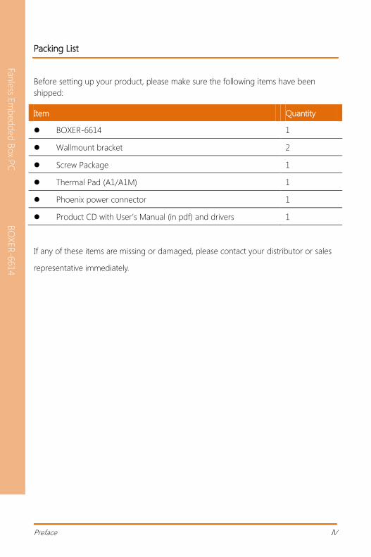
Packing List
Before setting up your product, please make sure the following items have been
shipped:
Item Quantity
BOXER-6614 1
Wallmount bracket 2
Screw Package 1
Thermal Pad (A1/A1M) 1
Phoenix power connector 1
Product CD with User’s Manual (in pdf) and drivers 1
If any of these items are missing or damaged, please contact your distributor or sales
representative immediately.
Preface V
Fanle
ss Em
bed
ded
Box P
C
BO
XER
-6614
About this Document
This User’s Manual contains all the essential information, such as detailed descriptions
and explanations on the product’s hardware and software features (if any), its
specifications, dimensions, jumper/connector settings/definitions, and driver
installation instructions (if any), to facilitate users in setting up their product.
Users may refer to the AAEON.com for the latest version of this document.

Preface VI
Fanle
ss Em
bed
ded
Box P
C
BO
XER
-6614
Safety Precautions
Please read the following safety instructions carefully. It is advised that you keep this
manual for future references
1. All cautions and warnings on the device should be noted.
2. Make sure the power source matches the power rating of the device.
3. Position the power cord so that people cannot step on it. Do not place anything
over the power cord.
4. Always completely disconnect the power before working on the system’s
hardware.
5. No connections should be made when the system is powered as a sudden rush
of power may damage sensitive electronic components.
6. If the device is not to be used for a long time, disconnect it from the power
supply to avoid damage by transient over-voltage.
7. Always disconnect this device from any AC supply before cleaning.
8. While cleaning, use a damp cloth instead of liquid or spray detergents.
9. Make sure the device is installed near a power outlet and is easily accessible.
10. Keep this device away from humidity.
11. Place the device on a solid surface during installation to prevent falls
12. Do not cover the openings on the device to ensure optimal heat dissipation.
13. Watch out for high temperatures when the system is running.
14. Do not touch the heat sink or heat spreader when the system is running
15. Never pour any liquid into the openings. This could cause fire or electric shock.
16. As most electronic components are sensitive to static electrical charge, be sure
to ground yourself to prevent static charge when installing the internal
components. Use a grounding wrist strap and contain all electronic components
in any static-shielded containers.

Preface VII
Fanle
ss Em
bed
ded
Box P
C
BO
XER
-6614
17. If any of the following situations arises, please the contact our service personnel:
i. Damaged power cord or plug
ii. Liquid intrusion to the device
iii. Exposure to moisture
iv. Device is not working as expected or in a manner as described in
this manual
v. The device is dropped or damaged
vi. Any obvious signs of damage displayed on the device
18. DO NOT LEAVE THIS DEVICE IN AN UNCONTROLLED ENVIRONMENT WITH
TEMPERATURES BEYOND THE DEVICE’S PERMITTED STORAGE TEMPERATURES
(SEE CHAPTER 1) TO PREVENT DAMAGE.
Preface VIII
Fanle
ss Em
bed
ded
Box P
C
BO
XER
-6614
FCC Statement
This device complies with Part 15 FCC Rules. Operation is
subject to the following two conditions: (1) this device may not
cause harmful interference, and (2) this device must accept
any interference received including interference that may
cause undesired operation.
Caution:
There is a danger of explosion if the battery is incorrectly replaced. Replace only with
the same or equivalent type recommended by the manufacturer. Dispose of used
batteries according to the manufacturer ’s instructions and your local government’s
recycling or disposal directives.
Attention:
Il y a un risque d’explosion si la batterie est remplacée de façon incorrecte.
Ne la remplacer qu’avec le même modèle ou équivalent recommandé par le
constructeur. Recycler les batteries usées en accord avec les instructions du fabricant et
les directives gouvernementales de recyclage.
Preface IX
Fanle
ss Em
bed
ded
Box P
C
BO
XER
-6614
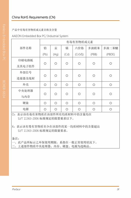
China RoHS Requirements (CN)
产品中有毒有害物质或元素名称及含量
AAEON Embedded Box PC/ Industrial System
部件名称
有毒有害物质或元素
铅
(Pb)
汞
(Hg)
镉
(Cd)
六价铬
(Cr(VI))
多溴联苯
(PBB)
多溴二苯醚
(PBDE)
印刷电路板
及其电子组件 ○ ○ ○ ○ ○ ○
外部信号
连接器及线材 ○ ○ ○ ○ ○ ○
外壳 ○ ○ ○ ○ ○ ○
中央处理器
与内存 ○ ○ ○ ○ ○ ○
硬盘 ○ ○ ○ ○ ○ ○
电源 ○ ○ ○ ○ ○ ○
O:表示该有毒有害物质在该部件所有均质材料中的含量均在
SJ/T 11363-2006 标准规定的限量要求以下。
X:表示该有毒有害物质至少在该部件的某一均质材料中的含量超出
SJ/T 11363-2006 标准规定的限量要求。
备注:
一、此产品所标示之环保使用期限,系指在一般正常使用状况下。
二、上述部件物质中央处理器、内存、硬盘、电源为选购品。
Preface X
Fanle
ss Em
bed
ded
Box P
C
BO
XER
-6614
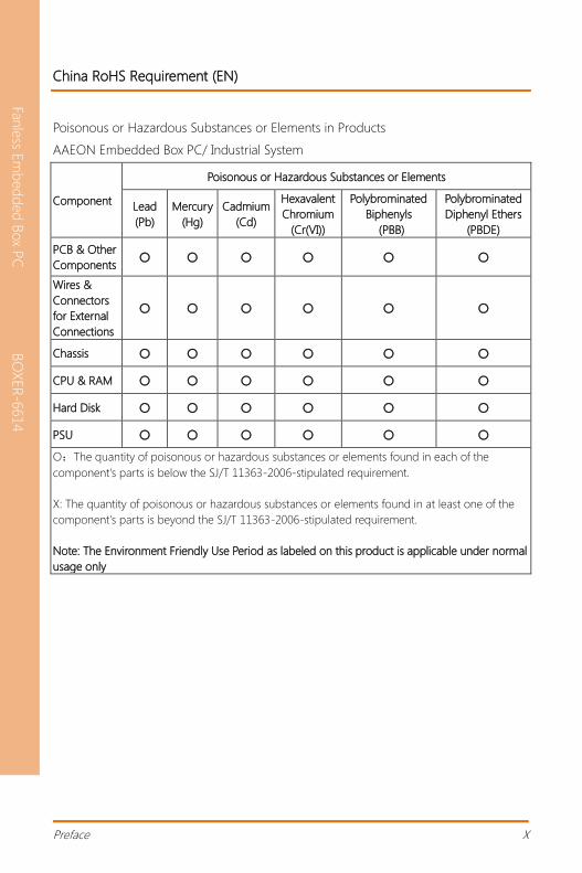
China RoHS Requirement (EN)
Poisonous or Hazardous Substances or Elements in Products
AAEON Embedded Box PC/ Industrial System
Component
Poisonous or Hazardous Substances or Elements
Lead
(Pb)
Mercury
(Hg)
Cadmium
(Cd)
Hexavalent
Chromium
(Cr(VI))
Polybrominated
Biphenyls
(PBB)
Polybrominated
Diphenyl Ethers
(PBDE)
PCB & Other
Components ○ ○ ○ ○ ○ ○
Wires &
Connectors
for External
Connections
○ ○ ○ ○ ○ ○
Chassis ○ ○ ○ ○ ○ ○
CPU & RAM ○ ○ ○ ○ ○ ○
Hard Disk ○ ○ ○ ○ ○ ○
PSU ○ ○ ○ ○ ○ ○
O:The quantity of poisonous or hazardous substances or elements found in each of the
component's parts is below the SJ/T 11363-2006-stipulated requirement.
X: The quantity of poisonous or hazardous substances or elements found in at least one of the
component's parts is beyond the SJ/T 11363-2006-stipulated requirement.
Note: The Environment Friendly Use Period as labeled on this product is applicable under normal
usage only
Preface XI
Fanle
ss Em
bed
ded
Box P
C
BO
XER
-6614
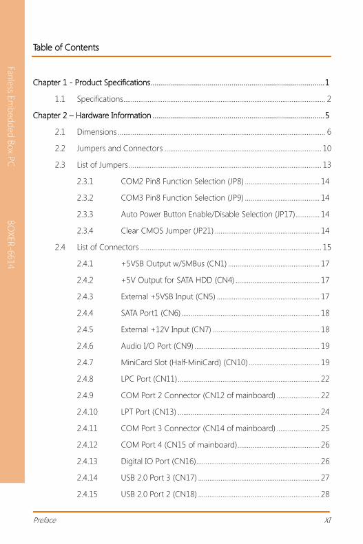
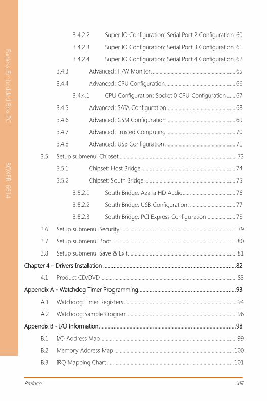
Table of Contents
Chapter 1 - Product Specifications ........................................................................................ 1
1.1 Specifications ............................................................................................................ 2
Chapter 2 – Hardware Information ....................................................................................... 5
2.1 Dimensions ............................................................................................................... 6
2.2 Jumpers and Connectors .................................................................................... 10
2.3 List of Jumpers ....................................................................................................... 13
2.3.1 COM2 Pin8 Function Selection (JP8) ........................................ 14
2.3.2 COM3 Pin8 Function Selection (JP9) ........................................ 14
2.3.3 Auto Power Button Enable/Disable Selection (JP17)............. 14
2.3.4 Clear CMOS Jumper (JP21) ........................................................ 14
2.4 List of Connectors ................................................................................................. 15
2.4.1 +5VSB Output w/SMBus (CN1) ................................................. 17
2.4.2 +5V Output for SATA HDD (CN4) ............................................. 17
2.4.3 External +5VSB Input (CN5) ....................................................... 17
2.4.4 SATA Port1 (CN6) .......................................................................... 18
2.4.5 External +12V Input (CN7) ......................................................... 18
2.4.6 Audio I/O Port (CN9) ................................................................... 19
2.4.7 MiniCard Slot (Half-MiniCard) (CN10) ...................................... 19
2.4.8 LPC Port (CN11) ............................................................................ 22
2.4.9 COM Port 2 Connector (CN12 of mainboard) ....................... 22
2.4.10 LPT Port (CN13) ............................................................................ 24
2.4.11 COM Port 3 Connector (CN14 of mainboard) ....................... 25
2.4.12 COM Port 4 (CN15 of mainboard) ............................................ 26
2.4.13 Digital IO Port (CN16) .................................................................. 26
2.4.14 USB 2.0 Port 3 (CN17) ................................................................. 27
2.4.15 USB 2.0 Port 2 (CN18) ................................................................. 28
Preface XII
Fanle
ss Em
bed
ded
Box P
C
BO
XER
-6614
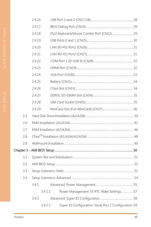
2.4.16 USB Port 2 and 3 (CN17/18) ...................................................... 28
2.4.17 BIOS Debug Port (CN19) ............................................................ 29
2.4.18 PS/2 Keyboard/Mouse Combo Port (CN22) ........................... 29
2.4.19 USB Ports 0 and 1 (CN25) ........................................................... 30
2.4.20 LAN (RJ-45) Port1 (CN26) ........................................................... 31
2.4.21 LAN (RJ-45) Port2 (CN27) ........................................................... 31
2.4.22 COM Port 1 (D-SUB 9) (CN28) .................................................. 32
2.4.23 HDMI Port (CN29) ........................................................................ 32
2.4.24 VGA Port (CN30) ........................................................................... 33
2.4.25 Battery (CN31)............................................................................... 34
2.4.26 CFast Slot (CN33) .......................................................................... 34
2.4.27 DDR3L SO-DIMM Slot (CN34) ................................................... 35
2.4.28 UIM Card Socket (CN35) ............................................................. 35
2.4.29 MiniCard Slot (Full-MiniCard) (CN37) ....................................... 36
2.5 Hard Disk Drive Installation (A2/A2M) .............................................................. 39
2.6 RAM Installation (A1/A1M).................................................................................. 41
2.7 RAM Installation (A2/A2M).................................................................................. 46
2.8 CFastTM
Installation (A1/A1M/A2/A2M) ............................................................ 48
2.9 Wallmount Installation .......................................................................................... 49
Chapter 3 - AMI BIOS Setup ................................................................................................ 50
3.1 System Test and Initialization .............................................................................. 51
3.2 AMI BIOS Setup ..................................................................................................... 52
3.3 Setup Submenu: Main .......................................................................................... 53
3.4 Setup Submenu: Advanced ................................................................................ 54
3.4.1 Advanced: Power Management ................................................ 55
3.4.1.1 Power Management: S5 RTC Wake Settings ............... 57
3.4.2 Advanced: Super IO Configuration........................................... 58
3.4.2.1 Super IO Configuration: Serial Port 1 Configuration . 59
Preface XIII
Fanle
ss Em
bed
ded
Box P
C
BO
XER
-6614
3.4.2.2 Super IO Configuration: Serial Port 2 Configuration . 60
3.4.2.3 Super IO Configuration: Serial Port 3 Configuration . 61
3.4.2.4 Super IO Configuration: Serial Port 4 Configuration . 62
3.4.3 Advanced: H/W Monitor ............................................................. 65
3.4.4 Advanced: CPU Configuration ................................................... 66
3.4.4.1 CPU Configuration: Socket 0 CPU Configuration ...... 67
3.4.5 Advanced: SATA Configuration .................................................. 68
3.4.6 Advanced: CSM Configuration .................................................. 69
3.4.7 Advanced: Trusted Computing .................................................. 70
3.4.8 Advanced: USB Configuration ................................................... 71
3.5 Setup submenu: Chipset...................................................................................... 73
3.5.1 Chipset: Host Bridge .................................................................... 74
3.5.2 Chipset: South Bridge .................................................................. 75
3.5.2.1 South Bridge: Azalia HD Audio ...................................... 76
3.5.2.2 South Bridge: USB Configuration .................................. 77
3.5.2.3 South Bridge: PCI Express Configuration ..................... 78
3.6 Setup submenu: Security ..................................................................................... 79
3.7 Setup submenu: Boot ........................................................................................... 80
3.8 Setup submenu: Save & Exit ............................................................................... 81
Chapter 4 – Drivers Installation ........................................................................................... 82
4.1 Product CD/DVD ................................................................................................... 83
Appendix A - Watchdog Timer Programming................................................................... 93
A.1 Watchdog Timer Registers .................................................................................. 94
A.2 Watchdog Sample Program ............................................................................... 96
Appendix B - I/O Information .............................................................................................. 98
B.1 I/O Address Map ................................................................................................... 99
B.2 Memory Address Map ....................................................................................... 100
B.3 IRQ Mapping Chart ............................................................................................ 101
Preface XIV
Fanle
ss Em
bed
ded
Box P
C
BO
XER
-6614
B.4 DMA Channel Assignments .............................................................................. 104

Fanle
ss Em
bed
ded
Box P
C
BO
XER
-6614
Chapter 1
Chapter 1 - Product Specifications
Chapter 1 – Product Specifications 2
Fanle
ss Em
bed
ded
Box P
C
BO
XER
-6614
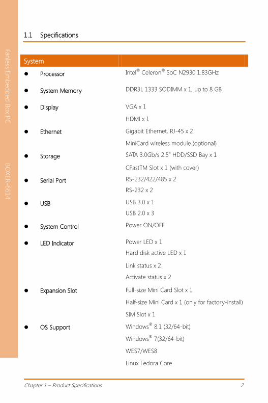
1.1 Specifications
System
Processor Intel®
Celeron®
SoC N2930 1.83GHz
System Memory DDR3L 1333 SODIMM x 1, up to 8 GB
Display VGA x 1
HDMI x 1
Ethernet Gigabit Ethernet, RJ-45 x 2
MiniCard wireless module (optional)
Storage SATA 3.0Gb/s 2.5” HDD/SSD Bay x 1
CFastTM Slot x 1 (with cover)
Serial Port RS-232/422/485 x 2
RS-232 x 2
USB USB 3.0 x 1
USB 2.0 x 3
System Control Power ON/OFF
LED Indicator Power LED x 1
Hard disk active LED x 1
Link status x 2
Activate status x 2
Expansion Slot Full-size Mini Card Slot x 1
Half-size Mini Card x 1 (only for factory-install)
SIM Slot x 1
OS Support Windows®
8.1 (32/64-bit)
Windows®
7(32/64-bit)
WES7/WES8
Linux Fedora Core
Chapter 1 – Product Specifications 3
Fanle
ss Em
bed
ded
Box P
C
BO
XER
-6614
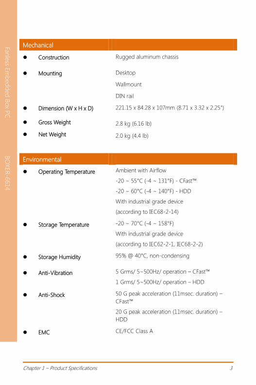
Mechanical
Construction Rugged aluminum chassis
Mounting Desktop
Wallmount
DIN rail
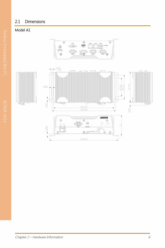
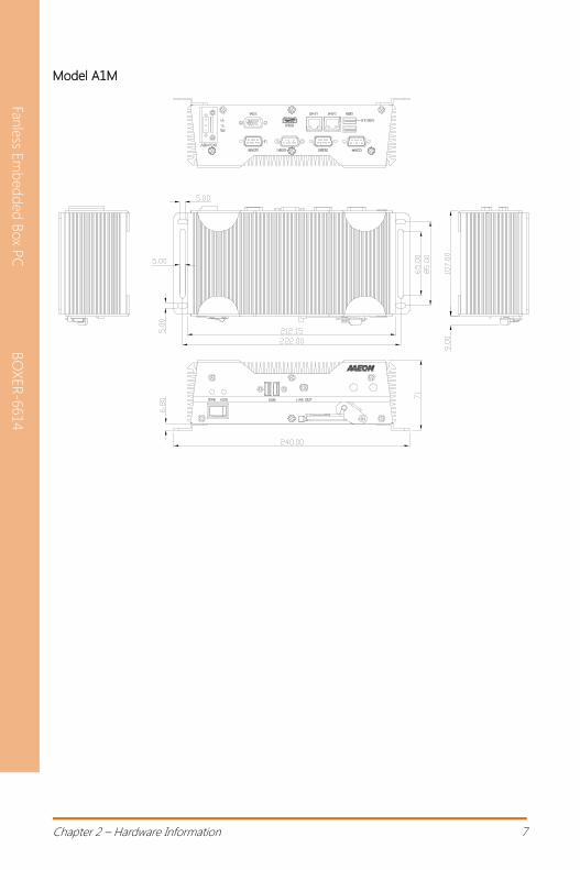
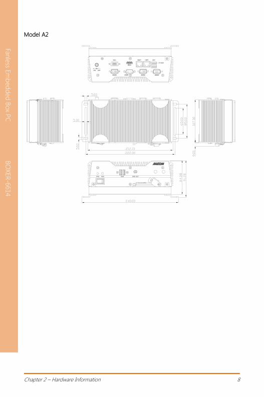
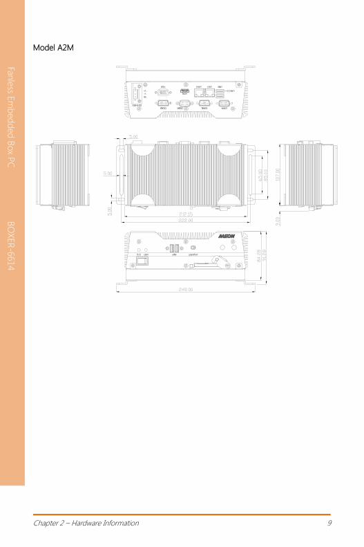
Dimension (W x H x D) 221.15 x 84.28 x 107mm (8.71 x 3.32 x 2.25")
Gross Weight 2.8 kg (6.16 lb)
Net Weight 2.0 kg (4.4 lb)
Environmental
Operating Temperature Ambient with Airflow
-20 ~ 55°C (-4 ~ 131°F) - CFast™
-20 ~ 60°C (-4 ~ 140°F) - HDD
With industrial grade device
(according to IEC68-2-14)
Storage Temperature -20 ~ 70°C (-4 ~ 158°F)
With industrial grade device
(according to IEC62-2-1, IEC68-2-2)
Storage Humidity 95% @ 40°C, non-condensing
Anti-Vibration 5 Grms/ 5~500Hz/ operation – CFast™
1 Grms/ 5~500Hz/ operation – HDD
Anti-Shock 50 G peak acceleration (11msec. duration) –
CFast™
20 G peak acceleration (11msec. duration) –
HDD
EMC CE/FCC Class A
Chapter 1 – Product Specifications 4
Fanle
ss Em
bed
ded
Box P
C
BO
XER
-6614
Power Supply
DC Input A1/A2 - DC power input 12V
A1M/A2M - DC 9-30V w/ 3-pin terminal block

Fanle
ss Em
bed
ded
Box P
C
BO
XER
-6614
Chapter 2
Chapter 2 – Hardware Information
Chapter 2 – Hardware Information 6
Fanle
ss Em
bed
ded
Box P
C
BO
XER
-6614
2.1 Dimensions
Model A1
--+12V DC
USB 3.0
Chapter 2 – Hardware Information 7
Fanle
ss Em
bed
ded
Box P
C
BO
XER
-6614
Model A1M
USB 3.0
Chapter 2 – Hardware Information 8
Fanle
ss Em
bed
ded
Box P
C
BO
XER
-6614
Model A2
--+12V DC
USB 3.0
Chapter 2 – Hardware Information 9
Fanle
ss Em
bed
ded
Box P
C
BO
XER
-6614
Model A2M
USB 3.0
Chapter 2 – Hardware Information 10
Fanle
ss Em
bed
ded
Box P
C
BO
XER
-6614
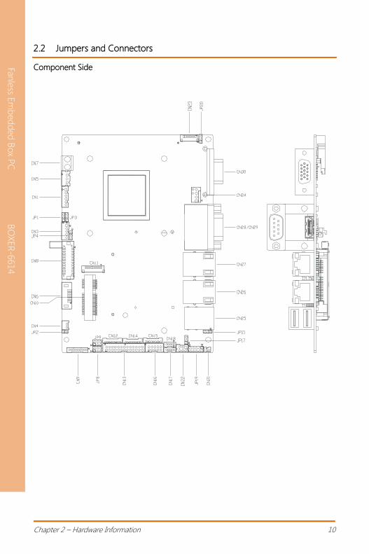
2.2 Jumpers and Connectors
Component Side
Chapter 2 – Hardware Information 11
Fanle
ss Em
bed
ded
Box P
C
BO
XER
-6614
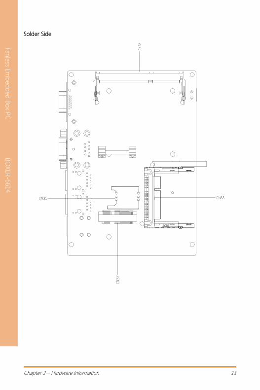
Solder Side
Chapter 2 – Hardware Information 12
Fanle
ss Em
bed
ded
Box P
C
BO
XER
-6614
Port 2(USB2.0 )
Port 3(USB2.0 )
USB 3.0
Port 0(USB3.0 )
Port 1(USB2.0 )
Chapter 2 – Hardware Information 13
Fanle
ss Em
bed
ded
Box P
C
BO
XER
-6614
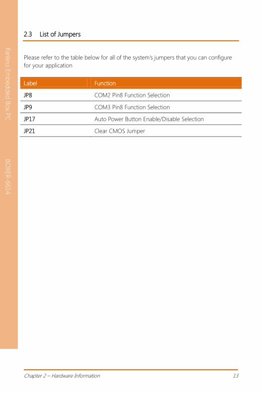
2.3 List of Jumpers
Please refer to the table below for all of the system’s jumpers that you can configure
for your application
Label Function
JP8 COM2 Pin8 Function Selection
JP9 COM3 Pin8 Function Selection
JP17 Auto Power Button Enable/Disable Selection
JP21 Clear CMOS Jumper
Chapter 2 – Hardware Information 14
Fanle
ss Em
bed
ded
Box P
C
BO
XER
-6614
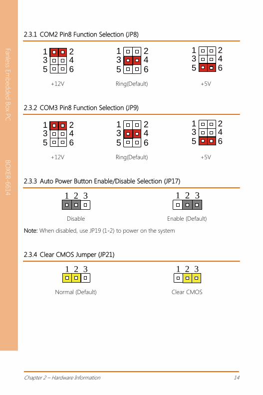
2.3.1 COM2 Pin8 Function Selection (JP8)
+12V Ring(Default) +5V
2.3.2 COM3 Pin8 Function Selection (JP9)
+12V Ring(Default) +5V
2.3.3 Auto Power Button Enable/Disable Selection (JP17)
Disable Enable (Default)
Note: When disabled, use JP19 (1-2) to power on the system
2.3.4 Clear CMOS Jumper (JP21)
Normal (Default) Clear CMOS
1 23 45 6
1 23 45 6
1 23 45 6
1 23 45 6
1 23 45 6
1 23 45 6
1 23 45 6
1 23 45 6
1 23 45 6
1 23 45 6
1 23 45 6
1 23 45 6
1 23 45 6
1 23 45 6
1 23 45 6
1 23 45 6
1 23 45 6
1 23 45 6
1 23 45 6
1 23 45 6
1 23 45 6
1 23 45 6
1 23 45 6
1 23 45 6
1 23 45 6
1 23 45 6
1 23 45 6
1 23 45 6
1 23 45 6
1 23 45 6
1 23 45 6
1 23 45 6
1 23 45 6
1 23 45 6
1 23 45 6
1 23 45 6
1 23 45 6
1 23 45 6
1 23 45 6
1 23 45 6
1 23 45 6
1 23 45 6
1 23 45 6
1 23 45 6
1 23 45 6
1 23 45 6
1 23 45 6
1 23 45 6
1 23 45 6
1 23 45 6
1 23 45 6
1 23 45 6
1 23 45 6
1 23 45 6
1 23 45 6
1 23 45 6
1 23 45 6
1 23 45 6
1 23 45 6
1 23 45 6
1 23 45 6
1 23 45 6
1 23 45 6
1 23 45 6
1 23 45 6
1 23 45 6
1 23 45 6
1 23 45 6
1 23 45 6
1 23 45 6
1 23 45 6
1 23 45 6
1 2 3 1 2 3
1 2 3 1 2 3
Chapter 2 – Hardware Information 15
Fanle
ss Em
bed
ded
Box P
C
BO
XER
-6614
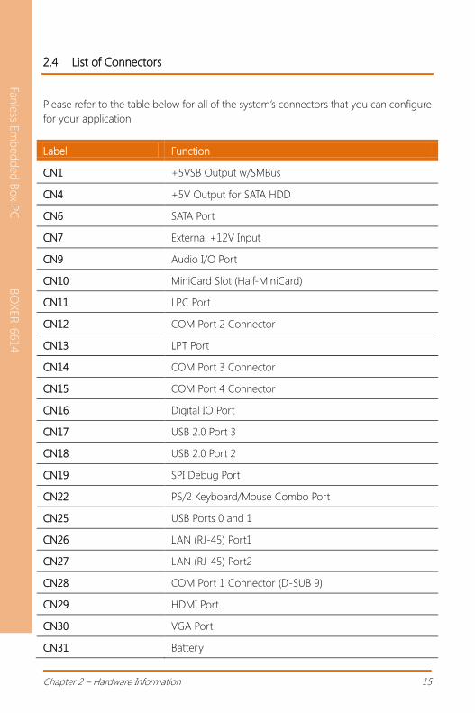
2.4 List of Connectors
Please refer to the table below for all of the system’s connectors that you can configure
for your application
Label Function
CN1 +5VSB Output w/SMBus
CN4 +5V Output for SATA HDD
CN6 SATA Port
CN7 External +12V Input
CN9 Audio I/O Port
CN10 MiniCard Slot (Half-MiniCard)
CN11 LPC Port
CN12 COM Port 2 Connector
CN13 LPT Port
CN14 COM Port 3 Connector
CN15 COM Port 4 Connector
CN16 Digital IO Port
CN17 USB 2.0 Port 3
CN18 USB 2.0 Port 2
CN19 SPI Debug Port
CN22 PS/2 Keyboard/Mouse Combo Port
CN25 USB Ports 0 and 1
CN26 LAN (RJ-45) Port1
CN27 LAN (RJ-45) Port2
CN28 COM Port 1 Connector (D-SUB 9)
CN29 HDMI Port
CN30 VGA Port
CN31 Battery
Chapter 2 – Hardware Information 16
Fanle
ss Em
bed
ded
Box P
C
BO
XER
-6614
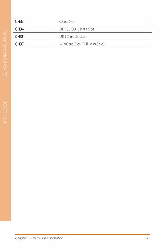
CN33 CFast Slot
CN34 DDR3L SO-DIMM Slot
CN35 UIM Card Socket
CN37 MiniCard Slot (Full-MiniCard)
Chapter 2 – Hardware Information 17
Fanle
ss Em
bed
ded
Box P
C
BO
XER
-6614
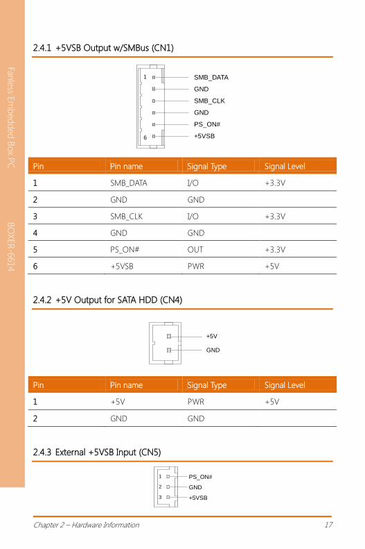
2.4.1 +5VSB Output w/SMBus (CN1)
Pin Pin name Signal Type Signal Level
1 SMB_DATA I/O +3.3V
2 GND GND
3 SMB_CLK I/O +3.3V
4 GND GND
5 PS_ON# OUT +3.3V
6 +5VSB PWR +5V
2.4.2 +5V Output for SATA HDD (CN4)
Pin Pin name Signal Type Signal Level
1 +5V PWR +5V
2 GND GND
2.4.3 External +5VSB Input (CN5)
SMB_DATA1
6
GND
SMB_CLK
GND
PS_ON#
+5VSB
+5V
GND
+5VSB
GND
PS_ON#1
2
3
Chapter 2 – Hardware Information 18
Fanle
ss Em
bed
ded
Box P
C
BO
XER
-6614
Pin Pin name Signal Type Signal Level
1 PS_ON# OUT +3.3V
2 GND GND
3 +5VSB PWR +5V
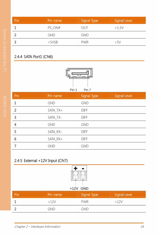
2.4.4 SATA Port1 (CN6)
Pin Pin name Signal Type Signal Level
1 GND GND
2 SATA_TX+ DIFF
3 SATA_TX- DIFF
4 GND GND
5 SATA_RX- DIFF
6 SATA_RX+ DIFF
7 GND GND
2.4.5 External +12V Input (CN7)
Pin Pin name Signal Type Signal Level
1 +12V PWR +12V
2 GND GND
Pin 1 Pin 7
+12V GND
Chapter 2 – Hardware Information 19
Fanle
ss Em
bed
ded
Box P
C
BO
XER
-6614
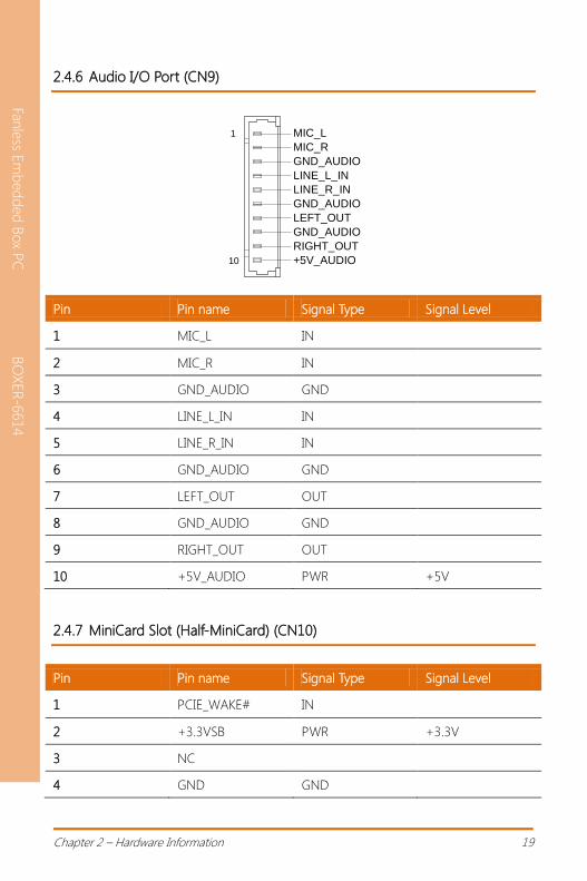
2.4.6 Audio I/O Port (CN9)
Pin Pin name Signal Type Signal Level
1 MIC_L IN
2 MIC_R IN
3 GND_AUDIO GND
4 LINE_L_IN IN
5 LINE_R_IN IN
6 GND_AUDIO GND
7 LEFT_OUT OUT
8 GND_AUDIO GND
9 RIGHT_OUT OUT
10 +5V_AUDIO PWR +5V
2.4.7 MiniCard Slot (Half-MiniCard) (CN10)
Pin Pin name Signal Type Signal Level
1 PCIE_WAKE# IN
2 +3.3VSB PWR +3.3V
3 NC
4 GND GND
MIC_L1
10
MIC_R
LINE_L_IN
LINE_R_IN
LEFT_OUT
RIGHT_OUT
+5V_AUDIO
GND_AUDIO
GND_AUDIO
GND_AUDIO
Chapter 2 – Hardware Information 20
Fanle
ss Em
bed
ded
Box P
C
BO
XER
-6614
5 NC
6 +1.5V PWR +1.5V
7 PCIE_CLK_REQ# IN
8 NC
9 GND GND
10 NC
11 PCIE_REF_CLK- DIFF
12 NC
13 PCIE_REF_CLK+ DIFF
14 NC
15 GND GND
16 NC
17 NC
18 GND GND
19 NC
20 W_DISABLE# OUT +3.3V
21 GND GND
22 PCIE_RST# OUT +3.3V
23 PCIE_RX- DIFF
24 +3.3VSB PWR +3.3V
25 PCIE_RX+ DIFF
26 GND GND
27 GND GND
28 +1.5V PWR +1.5V
29 GND GND
30 SMB_CLK I/O +3.3V
31 PCIE_TX- DIFF
32 SMB_DATA I/O +3.3V
Chapter 2 – Hardware Information 21
Fanle
ss Em
bed
ded
Box P
C
BO
XER
-6614
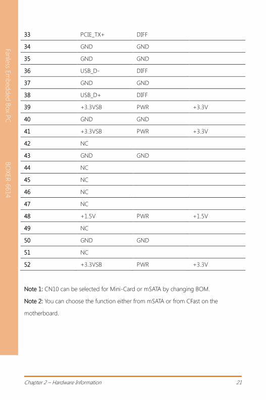
33 PCIE_TX+ DIFF
34 GND GND
35 GND GND
36 USB_D- DIFF
37 GND GND
38 USB_D+ DIFF
39 +3.3VSB PWR +3.3V
40 GND GND
41 +3.3VSB PWR +3.3V
42 NC
43 GND GND
44 NC
45 NC
46 NC
47 NC
48 +1.5V PWR +1.5V
49 NC
50 GND GND
51 NC
52 +3.3VSB PWR +3.3V
Note 1: CN10 can be selected for Mini-Card or mSATA by changing BOM.
Note 2: You can choose the function either from mSATA or from CFast on the
motherboard.
Chapter 2 – Hardware Information 22
Fanle
ss Em
bed
ded
Box P
C
BO
XER
-6614
2.4.8 LPC Port (CN11)
Pin Pin name Signal Type Signal Level
1 LAD0 I/O +3.3V
2 LAD1 I/O +3.3V
3 LAD2 I/O +3.3V
4 LAD3 I/O +3.3V
5 +3.3V PWR +3.3V
6 LFRAME# IN
7 LRESET# OUT +3.3V
8 GND GND
9 LCLK OUT
10 LDRQ0 IN
11 LDRQ1 IN
12 SERIRQ I/O +3.3V
2.4.9 COM Port 2 Connector (CN12 of mainboard)
LAD0 1
12
LAD1LAD2LAD3
LFRAME#LRESET#
LDRQ0LDRQ1
SERIRQ
GNDLCLK
+3.3V
1 5
6 9
Chapter 2 – Hardware Information 23
Fanle
ss Em
bed
ded
Box P
C
BO
XER
-6614
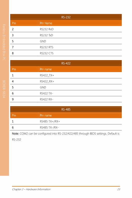
RS-232
Pin Pin Name
2 RS232 RxD
3 RS232 TxD
5 GND
7 RS232 RTS
8 RS232 CTS
RS-422
Pin Pin name
1 RS422_TX+
4 RS422_RX+
5 GND
6 RS422 TX-
9 RS422 RX-
RS-485
Pin Pin name
1 RS485 TX+/RX+
6 RS485 TX-/RX-
Note: COM2 can be configured into RS-232/422/485 through BIOS settings. Default is
RS-232
Chapter 2 – Hardware Information 24
Fanle
ss Em
bed
ded
Box P
C
BO
XER
-6614
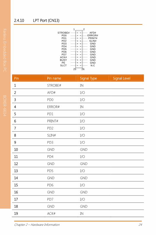
2.4.10 LPT Port (CN13)
Pin Pin name Signal Type Signal Level
1 STROBE# IN
2 AFD# I/O
3 PD0 I/O
4 ERROR# IN
5 PD1 I/O
6 PRINT# I/O
7 PD2 I/O
8 SLIN# I/O
9 PD3 I/O
10 GND GND
11 PD4 I/O
12 GND GND
13 PD5 I/O
14 GND GND
15 PD6 I/O
16 GND GND
17 PD7 I/O
18 GND GND
19 ACK# IN
N.C N.CN.CN.CN.CGNDGNDGNDGNDGNDGNDGNDGNDN.C
DIO0DIO1DIO2DIO3N.CN.CN.CN.C
DIO7DIO6DIO5DIO4
STROBE#
1 2
25 26
1 2
25 26
AFD#ERROR#PRINT#SLIN#GNDGNDGNDGNDGNDGNDGNDGNDN.C
PD0PD1PD2PD3PD4PD5PD6PD7
ACK#BUSY
PESLCT
DIO Mode
Chapter 2 – Hardware Information 25
Fanle
ss Em
bed
ded
Box P
C
BO
XER
-6614
20 GND GND
21 BUSY IN
22 GND GND
23 PE IN
24 GND GND
25 SLCT IN
26 NC
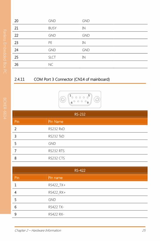
2.4.11 COM Port 3 Connector (CN14 of mainboard)
RS-232
Pin Pin Name
2 RS232 RxD
3 RS232 TxD
5 GND
7 RS232 RTS
8 RS232 CTS
RS-422
Pin Pin name
1 RS422_TX+
4 RS422_RX+
5 GND
6 RS422 TX-
9 RS422 RX-
1 5
6 9
Chapter 2 – Hardware Information 26
Fanle
ss Em
bed
ded
Box P
C
BO
XER
-6614
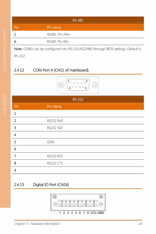
RS-485
Pin Pin name
1 RS485 TX+/RX+
6 RS485 TX-/RX-
Note: COM3 can be configured into RS-232/422/485 through BIOS settings. Default is
RS-232
2.4.12 COM Port 4 (CN15 of mainboard)
RS-232
Pin Pin Name
1
2 RS232 RxD
3 RS232 TxD
4
5 GND
6
7 RS232 RTS
8 RS232 CTS
9
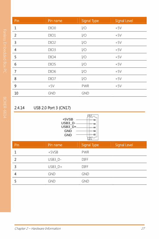
2.4.13 Digital IO Port (CN16)
1 5
6 9
Chapter 2 – Hardware Information 27
Fanle
ss Em
bed
ded
Box P
C
BO
XER
-6614
Pin Pin name Signal Type Signal Level
1 DIO0 I/O +5V
2 DIO1 I/O +5V
3 DIO2 I/O +5V
4 DIO3 I/O +5V
5 DIO4 I/O +5V
6 DIO5 I/O +5V
7 DIO6 I/O +5V
8 DIO7 I/O +5V
9 +5V PWR +5V
10 GND GND
2.4.14 USB 2.0 Port 3 (CN17)
Pin Pin name Signal Type Signal Level
1 +5VSB PWR
2 USB3_D- DIFF
3 USB3_D+ DIFF
4 GND GND
5 GND GND
+5VSBUSB3_D-USB3_D+
GND
GND
Chapter 2 – Hardware Information 28
Fanle
ss Em
bed
ded
Box P
C
BO
XER
-6614
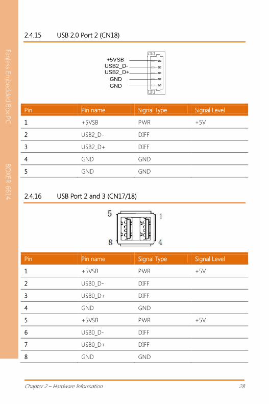
2.4.15 USB 2.0 Port 2 (CN18)
Pin Pin name Signal Type Signal Level
1 +5VSB PWR +5V
2 USB2_D- DIFF
3 USB2_D+ DIFF
4 GND GND
5 GND GND
2.4.16 USB Port 2 and 3 (CN17/18)
Pin Pin name Signal Type Signal Level
1 +5VSB PWR +5V
2 USB0_D- DIFF
3 USB0_D+ DIFF
4 GND GND
5 +5VSB PWR +5V
6 USB0_D- DIFF
7 USB0_D+ DIFF
8 GND GND
+5VSBUSB2_D-USB2_D+
GND
GND
Chapter 2 – Hardware Information 29
Fanle
ss Em
bed
ded
Box P
C
BO
XER
-6614
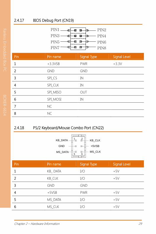
2.4.17 BIOS Debug Port (CN19)
Pin Pin name Signal Type Signal Level
1 +3.3VSB PWR +3.3V
2 GND GND
3 SPI_CS IN
4 SPI_CLK IN
5 SPI_MISO OUT
6 SPI_MOSI IN
7 NC
8 NC
2.4.18 PS/2 Keyboard/Mouse Combo Port (CN22)
Pin Pin name Signal Type Signal Level
1 KB_ DATA I/O +5V
2 KB_CLK I/O +5V
3 GND GND
4 +5VSB PWR +5V
5 MS_DATA I/O +5V
6 MS_CLK I/O +5V
PIN1
PIN3
PIN5
PIN7
PIN2
PIN4
PIN6
PIN8
KB_CLKKB_DATA1
5 6
2
MS_DATA
+5VSBGND
MS_CLK
Chapter 2 – Hardware Information 30
Fanle
ss Em
bed
ded
Box P
C
BO
XER
-6614
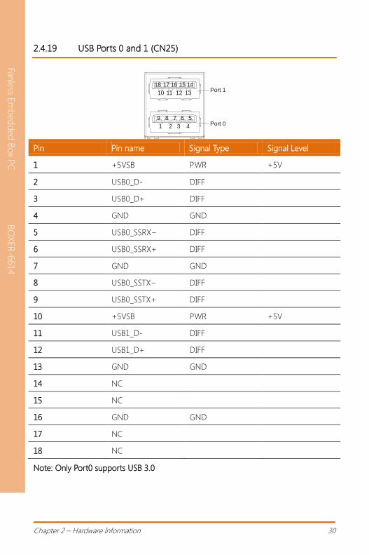
2.4.19 USB Ports 0 and 1 (CN25)
Pin Pin name Signal Type Signal Level
1 +5VSB PWR +5V
2 USB0_D- DIFF
3 USB0_D+ DIFF
4 GND GND
5 USB0_SSRX− DIFF
6 USB0_SSRX+ DIFF
7 GND GND
8 USB0_SSTX− DIFF
9 USB0_SSTX+ DIFF
10 +5VSB PWR +5V
11 USB1_D- DIFF
12 USB1_D+ DIFF
13 GND GND
14 NC
15 NC
16 GND GND
17 NC
18 NC
Note: Only Port0 supports USB 3.0
10Port 1
Port 0
11 12 13
1 2 3 4
1415161718
56789
Chapter 2 – Hardware Information 31
Fanle
ss Em
bed
ded
Box P
C
BO
XER
-6614
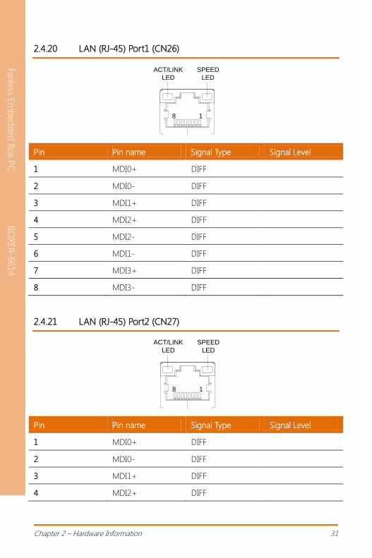
2.4.20 LAN (RJ-45) Port1 (CN26)
Pin Pin name Signal Type Signal Level
1 MDI0+ DIFF
2 MDI0- DIFF
3 MDI1+ DIFF
4 MDI2+ DIFF
5 MDI2- DIFF
6 MDI1- DIFF
7 MDI3+ DIFF
8 MDI3- DIFF
2.4.21 LAN (RJ-45) Port2 (CN27)
Pin Pin name Signal Type Signal Level
1 MDI0+ DIFF
2 MDI0- DIFF
3 MDI1+ DIFF
4 MDI2+ DIFF
1
ACT/LINK
LED
SPEED
LED
8
1
ACT/LINK
LED
SPEED
LED
8
Chapter 2 – Hardware Information 32
Fanle
ss Em
bed
ded
Box P
C
BO
XER
-6614
5 MDI2- DIFF
6 MDI1- DIFF
7 MDI3+ DIFF
8 MDI3- DIFF
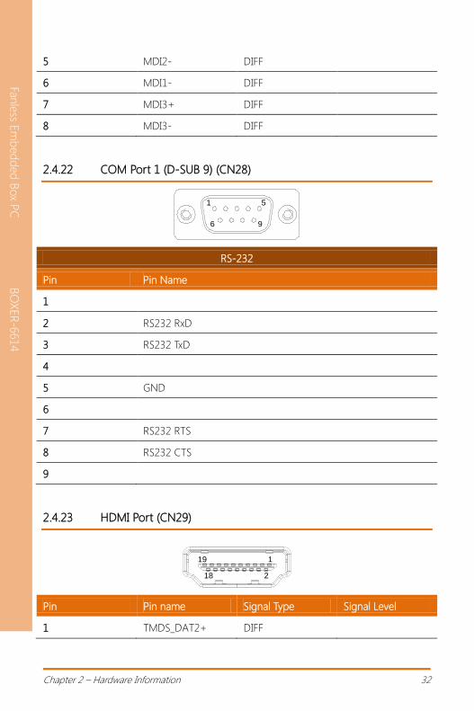
2.4.22 COM Port 1 (D-SUB 9) (CN28)
RS-232
Pin Pin Name
1
2 RS232 RxD
3 RS232 TxD
4
5 GND
6
7 RS232 RTS
8 RS232 CTS
9
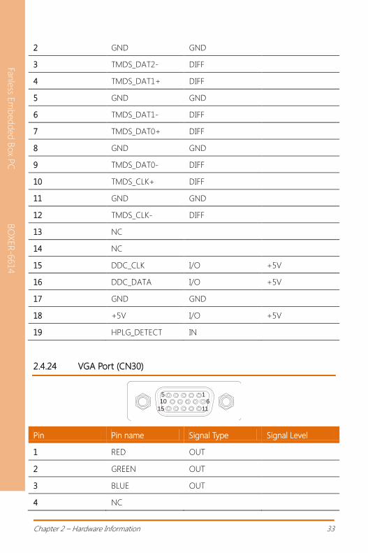
2.4.23 HDMI Port (CN29)
Pin Pin name Signal Type Signal Level
1 TMDS_DAT2+ DIFF
1 5
6 9
1
218
19
Chapter 2 – Hardware Information 33
Fanle
ss Em
bed
ded
Box P
C
BO
XER
-6614
2 GND GND
3 TMDS_DAT2- DIFF
4 TMDS_DAT1+ DIFF
5 GND GND
6 TMDS_DAT1- DIFF
7 TMDS_DAT0+ DIFF
8 GND GND
9 TMDS_DAT0- DIFF
10 TMDS_CLK+ DIFF
11 GND GND
12 TMDS_CLK- DIFF
13 NC
14 NC
15 DDC_CLK I/O +5V
16 DDC_DATA I/O +5V
17 GND GND
18 +5V I/O +5V
19 HPLG_DETECT IN
2.4.24 VGA Port (CN30)
Pin Pin name Signal Type Signal Level
1 RED OUT
2 GREEN OUT
3 BLUE OUT
4 NC
1610
1115
5
Chapter 2 – Hardware Information 34
Fanle
ss Em
bed
ded
Box P
C
BO
XER
-6614
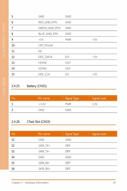
5 GND GND
6 RED_GND_RTN GND
7 GREEN_GND_RTN GND
8 BLUE_GND_RTN GND
9 +5V PWR +5V
10 CRT_PLUG#
11 NC
12 DDC_DATA I/O +5V
13 HSYNC OUT
14 VSYNC OUT
15 DDC_CLK I/O +5V
2.4.25 Battery (CN31)
Pin Pin name Signal Type Signal Level
1 +3.3V PWR 3.3V
2 GND GND
2.4.26 CFast Slot (CN33)
Pin Pin name Signal Type Signal Level
S1 GND GND
S2 SATA_TX+ DIFF
S3 SATA_TX- DIFF
S4 GND GND
S5 SATA_RX- DIFF
S6 SATA_RX+ DIFF
Chapter 2 – Hardware Information 35
Fanle
ss Em
bed
ded
Box P
C
BO
XER
-6614
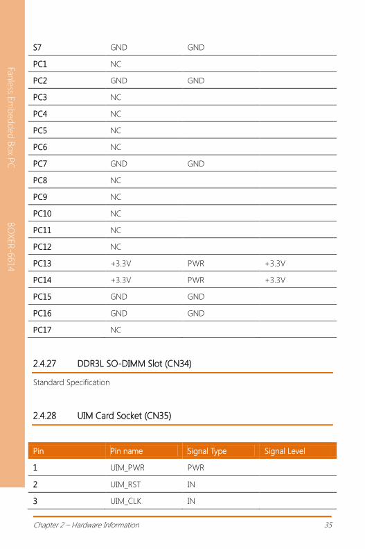
S7 GND GND
PC1 NC
PC2 GND GND
PC3 NC
PC4 NC
PC5 NC
PC6 NC
PC7 GND GND
PC8 NC
PC9 NC
PC10 NC
PC11 NC
PC12 NC
PC13 +3.3V PWR +3.3V
PC14 +3.3V PWR +3.3V
PC15 GND GND
PC16 GND GND
PC17 NC
2.4.27 DDR3L SO-DIMM Slot (CN34)
Standard Specification
2.4.28 UIM Card Socket (CN35)
Pin Pin name Signal Type Signal Level
1 UIM_PWR PWR
2 UIM_RST IN
3 UIM_CLK IN
Chapter 2 – Hardware Information 36
Fanle
ss Em
bed
ded
Box P
C
BO
XER
-6614
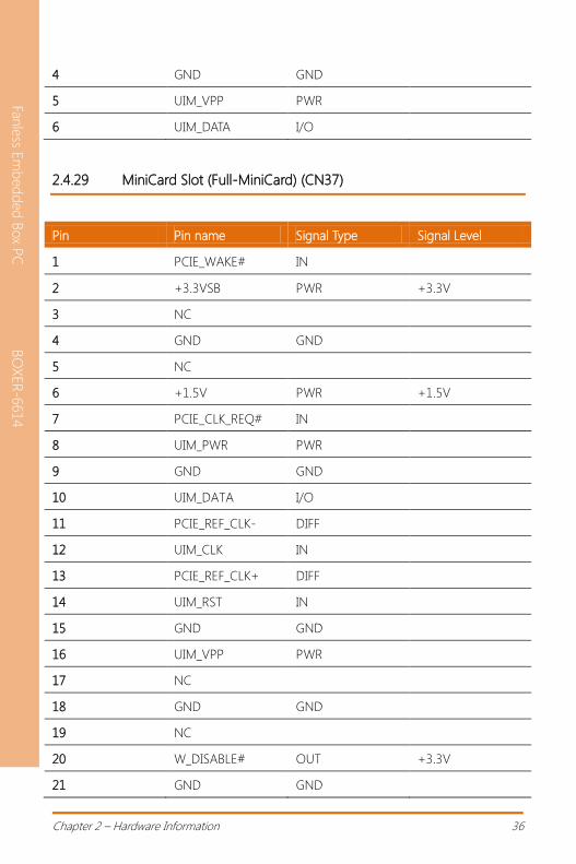
4 GND GND
5 UIM_VPP PWR
6 UIM_DATA I/O
2.4.29 MiniCard Slot (Full-MiniCard) (CN37)
Pin Pin name Signal Type Signal Level
1 PCIE_WAKE# IN
2 +3.3VSB PWR +3.3V
3 NC
4 GND GND
5 NC
6 +1.5V PWR +1.5V
7 PCIE_CLK_REQ# IN
8 UIM_PWR PWR
9 GND GND
10 UIM_DATA I/O
11 PCIE_REF_CLK- DIFF
12 UIM_CLK IN
13 PCIE_REF_CLK+ DIFF
14 UIM_RST IN
15 GND GND
16 UIM_VPP PWR
17 NC
18 GND GND
19 NC
20 W_DISABLE# OUT +3.3V
21 GND GND
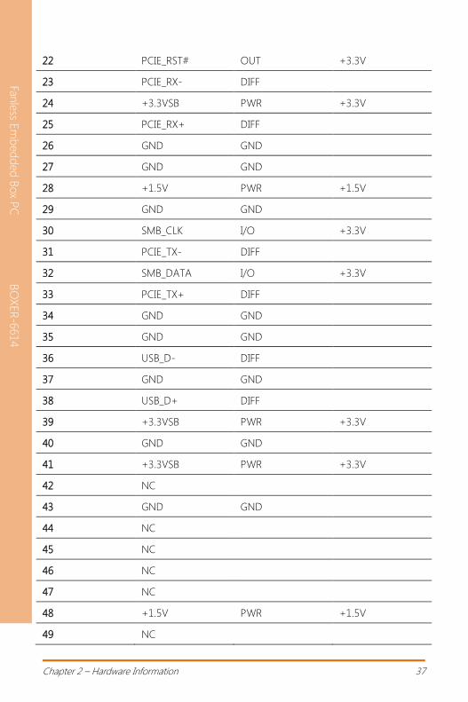
Chapter 2 – Hardware Information 37
Fanle
ss Em
bed
ded
Box P
C
BO
XER
-6614
22 PCIE_RST# OUT +3.3V
23 PCIE_RX- DIFF
24 +3.3VSB PWR +3.3V
25 PCIE_RX+ DIFF
26 GND GND
27 GND GND
28 +1.5V PWR +1.5V
29 GND GND
30 SMB_CLK I/O +3.3V
31 PCIE_TX- DIFF
32 SMB_DATA I/O +3.3V
33 PCIE_TX+ DIFF
34 GND GND
35 GND GND
36 USB_D- DIFF
37 GND GND
38 USB_D+ DIFF
39 +3.3VSB PWR +3.3V
40 GND GND
41 +3.3VSB PWR +3.3V
42 NC
43 GND GND
44 NC
45 NC
46 NC
47 NC
48 +1.5V PWR +1.5V
49 NC
Chapter 2 – Hardware Information 38
Fanle
ss Em
bed
ded
Box P
C
BO
XER
-6614
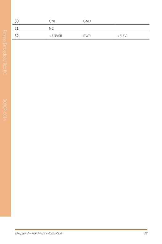
50 GND GND
51 NC
52 +3.3VSB PWR +3.3V
Chapter 2 – Hardware Information 39
Fanle
ss Em
bed
ded
Box P
C
BO
XER
-6614
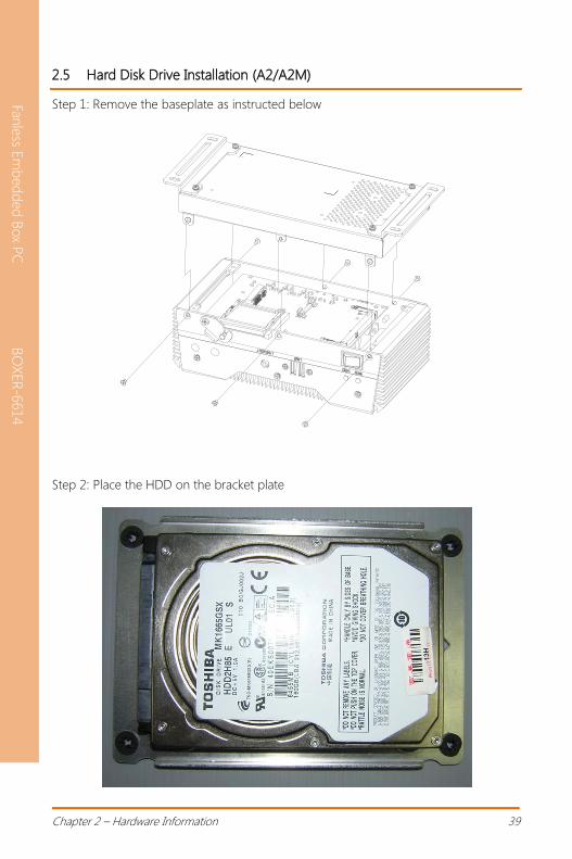
2.5 Hard Disk Drive Installation (A2/A2M)
Step 1: Remove the baseplate as instructed below
Step 2: Place the HDD on the bracket plate
Chapter 2 – Hardware Information 40
Fanle
ss Em
bed
ded
Box P
C
BO
XER
-6614
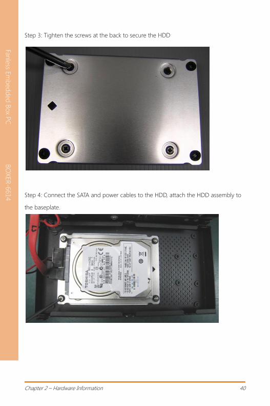
Step 3: Tighten the screws at the back to secure the HDD
Step 4: Connect the SATA and power cables to the HDD, attach the HDD assembly to
the baseplate.
Chapter 2 – Hardware Information 41
Fanle
ss Em
bed
ded
Box P
C
BO
XER
-6614
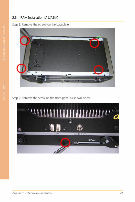
2.6 RAM Installation (A1/A1M)
Step 1: Remove the screws on the baseplate
Step 2: Remove the screw on the front panel as shown below
Chapter 2 – Hardware Information 42
Fanle
ss Em
bed
ded
Box P
C
BO
XER
-6614
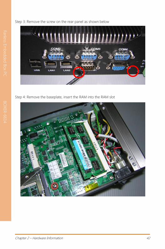
Step 3: Remove the screw on the rear panel as shown below
Step 4: Remove the baseplate, insert the RAM into the RAM slot
Chapter 2 – Hardware Information 43
Fanle
ss Em
bed
ded
Box P
C
BO
XER
-6614
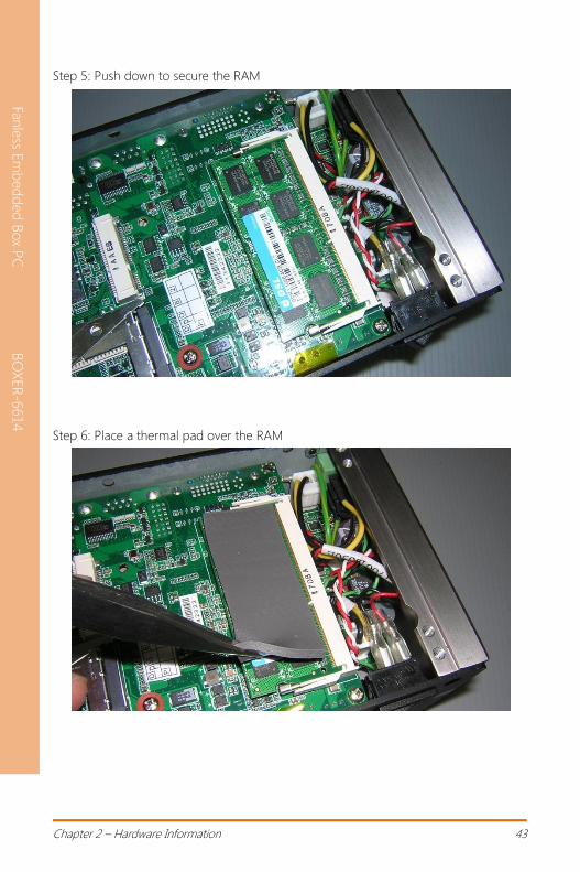
Step 5: Push down to secure the RAM
Step 6: Place a thermal pad over the RAM
Chapter 2 – Hardware Information 44
Fanle
ss Em
bed
ded
Box P
C
BO
XER
-6614
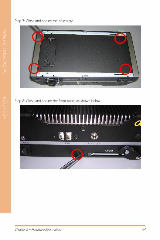
Step 7: Close and secure the baseplate
Step 8: Close and secure the front panel as shown below
Chapter 2 – Hardware Information 45
Fanle
ss Em
bed
ded
Box P
C
BO
XER
-6614
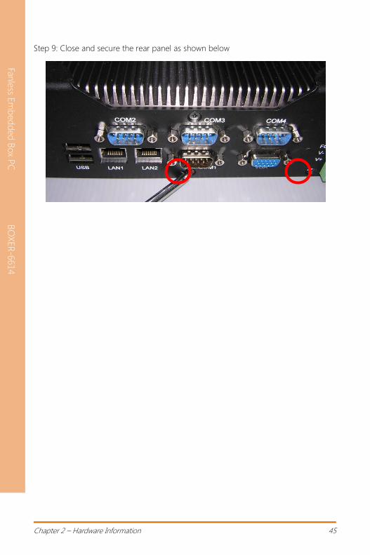
Step 9: Close and secure the rear panel as shown below
Chapter 2 – Hardware Information 46
Fanle
ss Em
bed
ded
Box P
C
BO
XER
-6614
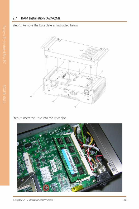
2.7 RAM Installation (A2/A2M)
Step 1: Remove the baseplate as instructed below
Step 2: Insert the RAM into the RAM slot
Chapter 2 – Hardware Information 47
Fanle
ss Em
bed
ded
Box P
C
BO
XER
-6614
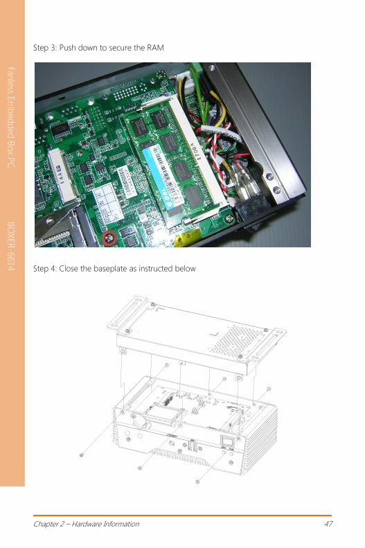
Step 3: Push down to secure the RAM
Step 4: Close the baseplate as instructed below
Chapter 2 – Hardware Information 48
Fanle
ss Em
bed
ded
Box P
C
BO
XER
-6614
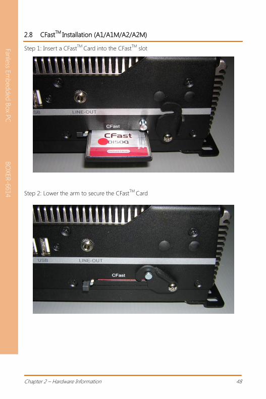
2.8 CFastTM
Installation (A1/A1M/A2/A2M)
Step 1: Insert a CFastTM
Card into the CFastTM
slot
Step 2: Lower the arm to secure the CFastTM
Card
Chapter 2 – Hardware Information 49
Fanle
ss Em
bed
ded
Box P
C
BO
XER
-6614
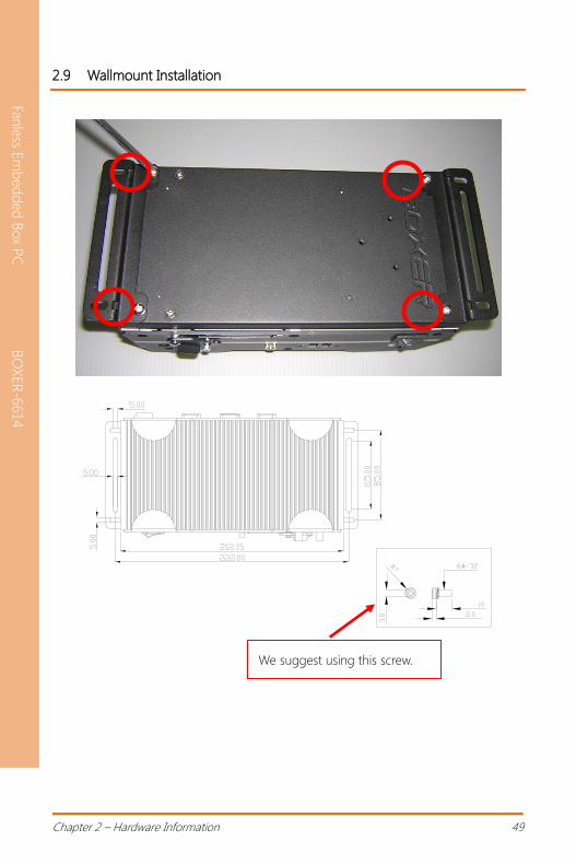
2.9 Wallmount Installation
We suggest using this screw.

Fanle
ss Em
bed
ded
Box P
C
BO
XER
-6614
Chapter 3
Chapter 3 - AMI BIOS Setup

Chapter 3 – AMI BIOS Setup 51
Fanle
ss Em
bed
ded
Box P
C
BO
XER
-6614
3.1 System Test and Initialization
The system uses certain routines to perform testing and initialization. If an error, fatal or
non-fatal, is encountered, a few short beeps or an error message will be outputted. The
board can usually continue the boot up sequence with non-fatal errors.
The system configuration verification routines check the current system configuration
against the values stored in the CMOS memory. If they do not match, an error message
will be outputted, in which case you will need to run the BIOS setup program to set the
configuration information in memory.
There are three situations in which you will need to change the CMOS settings:
- You are starting your system for the first time
- You have changed your system’s hardware
- The CMOS memory has lost power and the configuration information is erased
The system’s CMOS memory uses a backup battery for data retention, which is to be
replaced once emptied.
Chapter 3 – AMI BIOS Setup 52
Fanle
ss Em
bed
ded
Box P
C
BO
XER
-6614
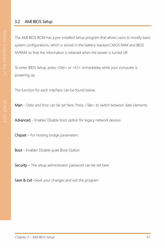
3.2 AMI BIOS Setup
The AMI BIOS ROM has a pre-installed Setup program that allows users to modify basic
system configurations, which is stored in the battery-backed CMOS RAM and BIOS
NVRAM so that the information is retained when the power is turned off.
To enter BIOS Setup, press <Del> or <F2> immediately while your computer is
powering up.
The function for each interface can be found below.
Main – Date and time can be set here. Press <Tab> to switch between date elements
Advanced – Enable/ Disable boot option for legacy network devices
Chipset – For hosting bridge parameters
Boot – Enable/ Disable quiet Boot Option
Security – The setup administrator password can be set here
Save & Exit –Save your changes and exit the program
Chapter 3 – AMI BIOS Setup 53
Fanle
ss Em
bed
ded
Box P
C
BO
XER
-6614
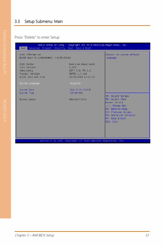
3.3 Setup Submenu: Main
Press “Delete” to enter Setup

Chapter 3 – AMI BIOS Setup 54
Fanle
ss Em
bed
ded
Box P
C
BO
XER
-6614
3.4 Setup Submenu: Advanced
Chapter 3 – AMI BIOS Setup 55
Fanle
ss Em
bed
ded
Box P
C
BO
XER
-6614
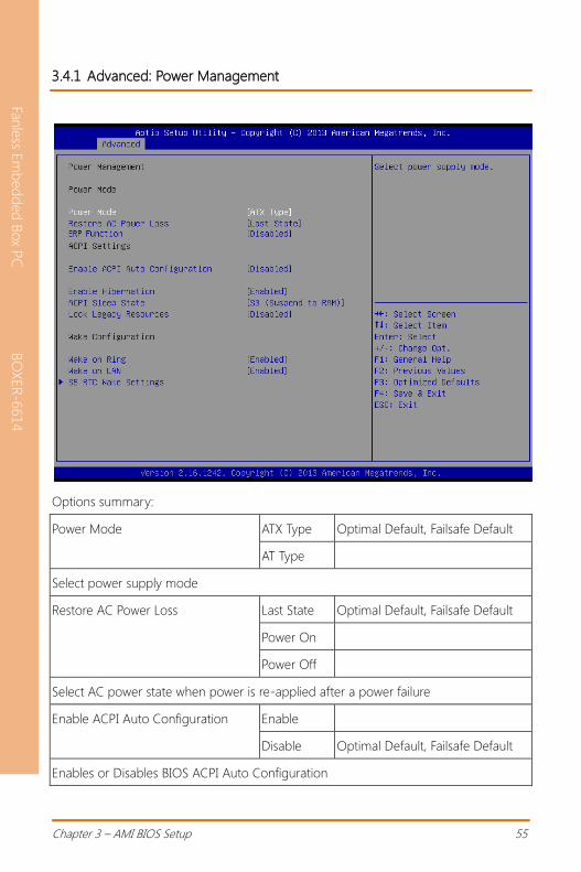
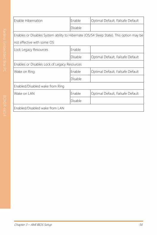
3.4.1 Advanced: Power Management
Options summary:
Power Mode ATX Type Optimal Default, Failsafe Default
AT Type
Select power supply mode
Restore AC Power Loss Last State Optimal Default, Failsafe Default
Power On
Power Off
Select AC power state when power is re-applied after a power failure
Enable ACPI Auto Configuration Enable
Disable Optimal Default, Failsafe Default
Enables or Disables BIOS ACPI Auto Configuration
Chapter 3 – AMI BIOS Setup 56
Fanle
ss Em
bed
ded
Box P
C
BO
XER
-6614
Enable Hibernation Enable Optimal Default, Failsafe Default
Disable
Enables or Disables System ability to Hibernate (OS/S4 Sleep State). This option may be
not effective with some OS
Lock Legacy Resources Enable
Disable Optimal Default, Failsafe Default
Enables or Disables Lock of Legacy Resources
Wake on Ring Enable Optimal Default, Failsafe Default
Disable
Enabled/Disabled wake from Ring
Wake on LAN Enable Optimal Default, Failsafe Default
Disable
Enabled/Disabled wake from LAN
Chapter 3 – AMI BIOS Setup 57
Fanle
ss Em
bed
ded
Box P
C
BO
XER
-6614
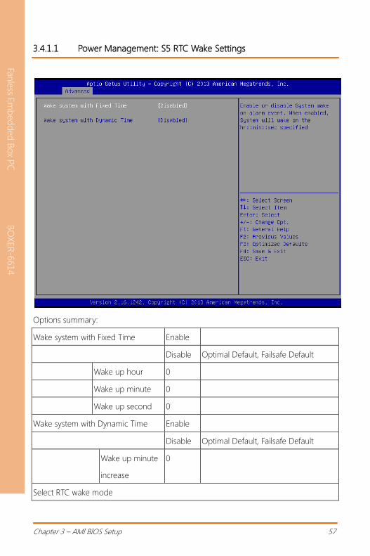
3.4.1.1 Power Management: S5 RTC Wake Settings
Options summary:
Wake system with Fixed Time Enable
Disable Optimal Default, Failsafe Default
Wake up hour 0
Wake up minute 0
Wake up second 0
Wake system with Dynamic Time Enable
Disable Optimal Default, Failsafe Default
Wake up minute
increase
0
Select RTC wake mode
Chapter 3 – AMI BIOS Setup 58
Fanle
ss Em
bed
ded
Box P
C
BO
XER
-6614
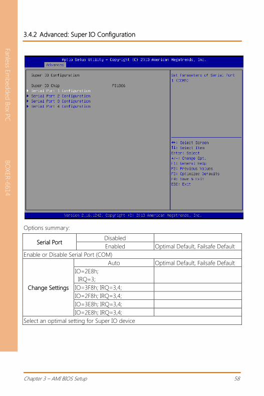
3.4.2 Advanced: Super IO Configuration
Options summary:
Serial Port Disabled
Enabled Optimal Default, Failsafe Default
Enable or Disable Serial Port (COM)
Change Settings
Auto Optimal Default, Failsafe Default
IO=2E8h;
IRQ=3;
IO=3F8h; IRQ=3,4;
IO=2F8h; IRQ=3,4;
IO=3E8h; IRQ=3,4;
IO=2E8h; IRQ=3,4;
Select an optimal setting for Super IO device
Chapter 3 – AMI BIOS Setup 59
Fanle
ss Em
bed
ded
Box P
C
BO
XER
-6614
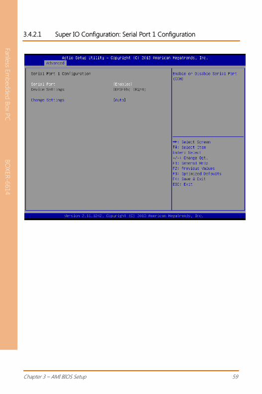
3.4.2.1 Super IO Configuration: Serial Port 1 Configuration

Chapter 3 – AMI BIOS Setup 60
Fanle
ss Em
bed
ded
Box P
C
BO
XER
-6614
3.4.2.2 Super IO Configuration: Serial Port 2 Configuration

Chapter 3 – AMI BIOS Setup 61
Fanle
ss Em
bed
ded
Box P
C
BO
XER
-6614
3.4.2.3 Super IO Configuration: Serial Port 3 Configuration
Chapter 3 – AMI BIOS Setup 62
Fanle
ss Em
bed
ded
Box P
C
BO
XER
-6614
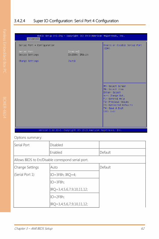
3.4.2.4 Super IO Configuration: Serial Port 4 Configuration
Options summary:
Serial Port Disabled
Enabled Default
Allows BIOS to En/Disable correspond serial port.
Change Settings
(Serial Port 1)
Auto Default
IO=3F8h; IRQ=4;
IO=3F8h;
IRQ=3,4,5,6,7,9,10,11,12;
IO=2F8h;
IRQ=3,4,5,6,7,9,10,11,12;
Chapter 3 – AMI BIOS Setup 63
Fanle
ss Em
bed
ded
Box P
C
BO
XER
-6614
IO=3E8h;
IRQ=3,4,5,6,7,9,10,11,12;
IO=2E8h;
IRQ=3,4,5,6,7,9,10,11,12;
Allows BIOS to Select Serial Port resource.
Change Settings
(Serial Port 2)
Auto Default
IO=2F8h; IRQ=3;
IO=3F8h;
IRQ=3,4,5,6,7,9,10,11,12;
IO=2F8h;
IRQ=3,4,5,6,7,9,10,11,12;
IO=3E8h;
IRQ=3,4,5,6,7,9,10,11,12;
IO=2E8h;
IRQ=3,4,5,6,7,9,10,11,12;
Working model RS232 Default
RS422
RS485
Select Working model
Change Settings
(Serial Port 3)
Auto Default
IO=3E8h; IRQ=7;
IO=3E8h;
IRQ=3,4,5,6,7,9,10,11,12;
IO=2E8h;
IRQ=3,4,5,6,7,9,10,11,12;
IO=3E8h;
IRQ=3,4,5,6,7,9,10,11,12;
Chapter 3 – AMI BIOS Setup 64
Fanle
ss Em
bed
ded
Box P
C
BO
XER
-6614
IO=2E8h;
IRQ=3,4,5,6,7,9,10,11,12;
Working model RS232 Default
RS422
RS485
Select Working model
Change Settings
(Serial Port 4)
Auto Default
IO=2E8h; IRQ=7;
IO=3F8h;
IRQ=3,4,5,6,7,9,10,11,12;
IO=2F8h;
IRQ=3,4,5,6,7,9,10,11,12;
IO=3E8h;
IRQ=3,4,5,6,7,9,10,11,12;
IO=2E8h;
IRQ=3,4,5,6,7,9,10,11,12;
Allows BIOS to Select Serial Port resource.
Smart Fan Function Enable
Disable Optimal Default, Failsafe Default
Enable or Disable Smart Fan
Chapter 3 – AMI BIOS Setup 65
Fanle
ss Em
bed
ded
Box P
C
BO
XER
-6614
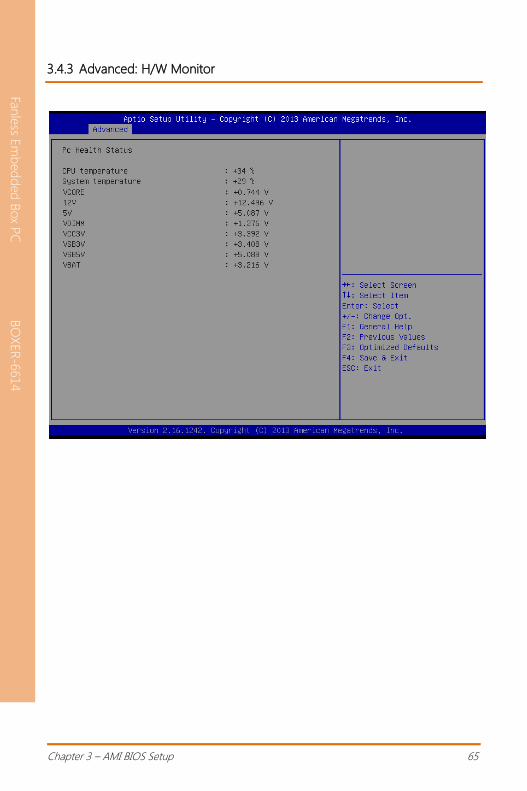
3.4.3 Advanced: H/W Monitor

Chapter 3 – AMI BIOS Setup 66
Fanle
ss Em
bed
ded
Box P
C
BO
XER
-6614
3.4.4 Advanced: CPU Configuration
Options summary:
Intel Virtualization
Technology
Disabled
Enabled Optimal Default, Failsafe Default
When enabled, a VMM can utilize the additional hardware capabilities provided by
Vander pool Technology

Chapter 3 – AMI BIOS Setup 67
Fanle
ss Em
bed
ded
Box P
C
BO
XER
-6614
3.4.4.1 CPU Configuration: Socket 0 CPU Configuration
Chapter 3 – AMI BIOS Setup 68
Fanle
ss Em
bed
ded
Box P
C
BO
XER
-6614
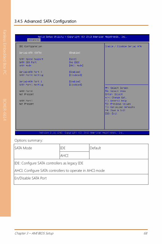
3.4.5 Advanced: SATA Configuration
Options summary:
SATA Mode IDE Default
AHCI
IDE: Configure SATA controllers as legacy IDE
AHCI: Configure SATA controllers to operate in AHCI mode
En/Disable SATA Port

Chapter 3 – AMI BIOS Setup 69
Fanle
ss Em
bed
ded
Box P
C
BO
XER
-6614
3.4.6 Advanced: CSM Configuration
Chapter 3 – AMI BIOS Setup 70
Fanle
ss Em
bed
ded
Box P
C
BO
XER
-6614
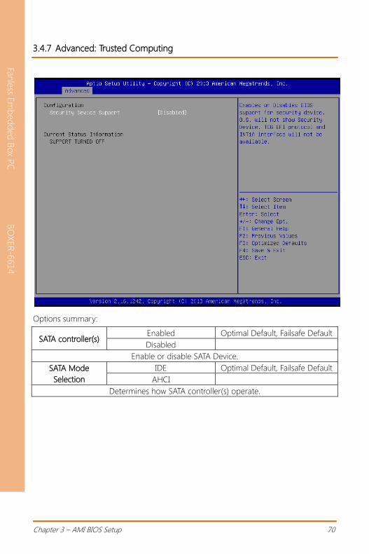
3.4.7 Advanced: Trusted Computing
Options summary:
SATA controller(s) Enabled Optimal Default, Failsafe Default
Disabled
Enable or disable SATA Device.
SATA Mode
Selection
IDE Optimal Default, Failsafe Default
AHCI
Determines how SATA controller(s) operate.
Chapter 3 – AMI BIOS Setup 71
Fanle
ss Em
bed
ded
Box P
C
BO
XER
-6614
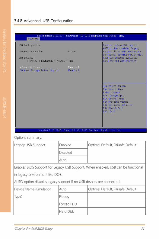
3.4.8 Advanced: USB Configuration
Options summary:
Legacy USB Support Enabled Optimal Default, Failsafe Default
Disabled
Auto
Enables BIOS Support for Legacy USB Support. When enabled, USB can be functional
in legacy environment like DOS.
AUTO option disables legacy support if no USB devices are connected
Device Name (Emulation
Type)
Auto Optimal Default, Failsafe Default
Floppy
Forced FDD
Hard Disk

Chapter 3 – AMI BIOS Setup 72
Fanle
ss Em
bed
ded
Box P
C
BO
XER
-6614
CDROM
If Auto. USB devices less than 530MB will be emulated as Floppy and remaining as
Floppy and remaining as hard drive. Forced FDD option can be used to force a HDD
formatted drive to boot as FDD(Ex. ZIP drive)
Chapter 3 – AMI BIOS Setup 73
Fanle
ss Em
bed
ded
Box P
C
BO
XER
-6614
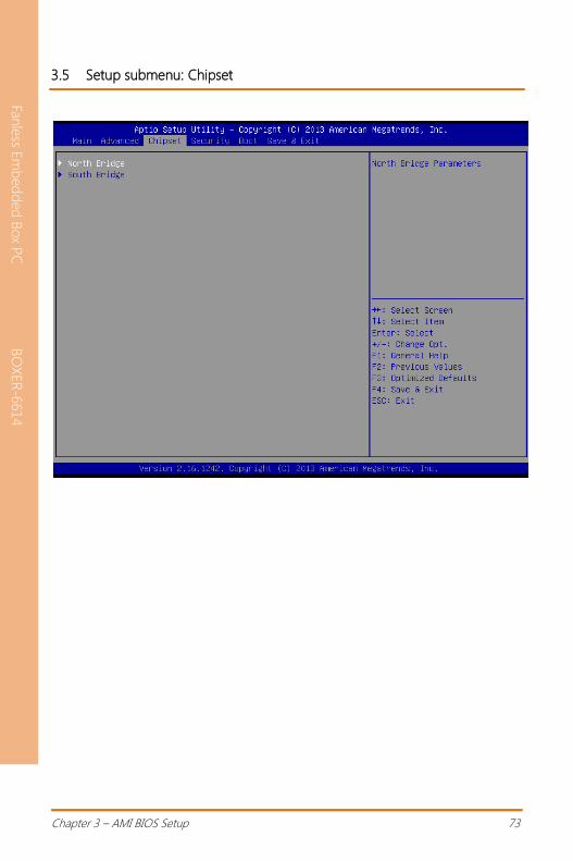
3.5 Setup submenu: Chipset
Chapter 3 – AMI BIOS Setup 74
Fanle
ss Em
bed
ded
Box P
C
BO
XER
-6614
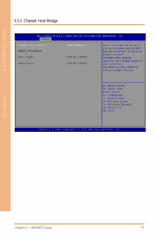
3.5.1 Chipset: Host Bridge
Chapter 3 – AMI BIOS Setup 75
Fanle
ss Em
bed
ded
Box P
C
BO
XER
-6614
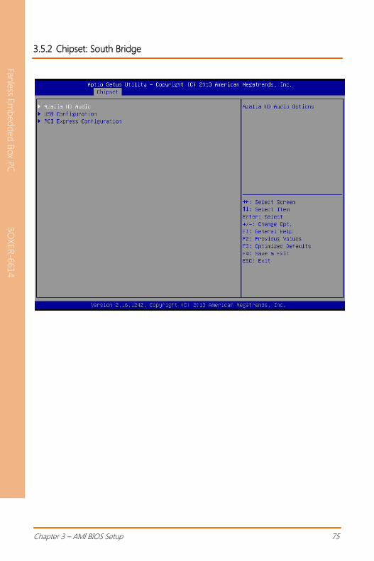
3.5.2 Chipset: South Bridge
Chapter 3 – AMI BIOS Setup 76
Fanle
ss Em
bed
ded
Box P
C
BO
XER
-6614
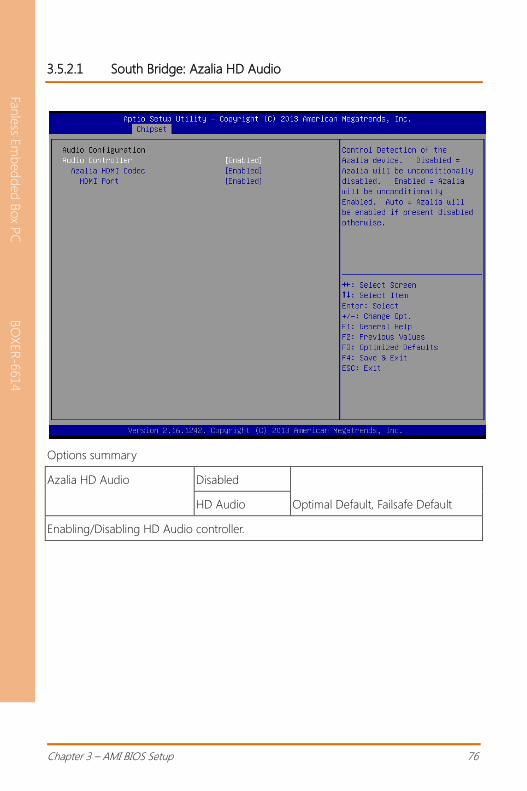
3.5.2.1 South Bridge: Azalia HD Audio
Options summary
Azalia HD Audio Disabled
HD Audio Optimal Default, Failsafe Default
Enabling/Disabling HD Audio controller.
Chapter 3 – AMI BIOS Setup 77
Fanle
ss Em
bed
ded
Box P
C
BO
XER
-6614
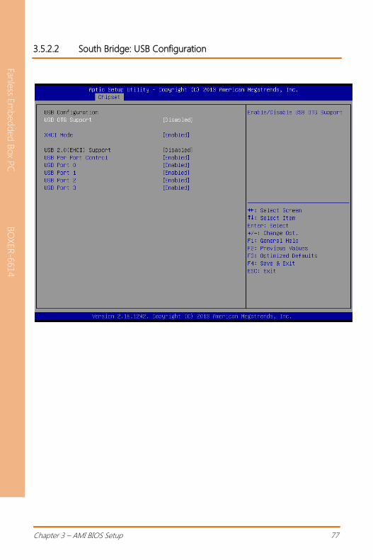
3.5.2.2 South Bridge: USB Configuration
Chapter 3 – AMI BIOS Setup 78
Fanle
ss Em
bed
ded
Box P
C
BO
XER
-6614
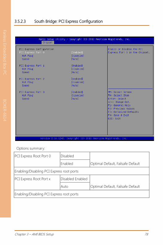
3.5.2.3 South Bridge: PCI Express Configuration
Options summary:
PCI Express Root Port 0 Disabled
Enabled Optimal Default, Failsafe Default
Enabling/Disabling PCI Express root ports
PCI Express Root Port x Disabled Enabled
Auto Optimal Default, Failsafe Default
Enabling/Disabling PCI Express root ports
Chapter 3 – AMI BIOS Setup 79
Fanle
ss Em
bed
ded
Box P
C
BO
XER
-6614
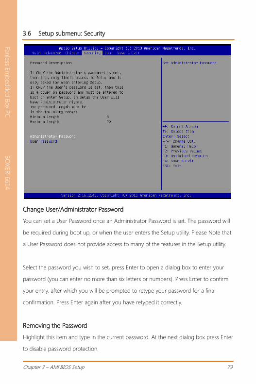
3.6 Setup submenu: Security
Change User/Administrator Password
You can set a User Password once an Administrator Password is set. The password will
be required during boot up, or when the user enters the Setup utility. Please Note that
a User Password does not provide access to many of the features in the Setup utility.
Select the password you wish to set, press Enter to open a dialog box to enter your
password (you can enter no more than six letters or numbers). Press Enter to confirm
your entry, after which you will be prompted to retype your password for a final
confirmation. Press Enter again after you have retyped it correctly.
Removing the Password
Highlight this item and type in the current password. At the next dialog box press Enter
to disable password protection.
Chapter 3 – AMI BIOS Setup 80
Fanle
ss Em
bed
ded
Box P
C
BO
XER
-6614
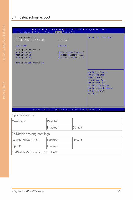
3.7 Setup submenu: Boot
Options summary:
Quiet Boot Disabled
Enabled Default
En/Disable showing boot logo.
Launch i210/i211 PXE
OpROM
Disabled Default
Enabled
En/Disable PXE boot for 8111E LAN
Chapter 3 – AMI BIOS Setup 81
Fanle
ss Em
bed
ded
Box P
C
BO
XER
-6614
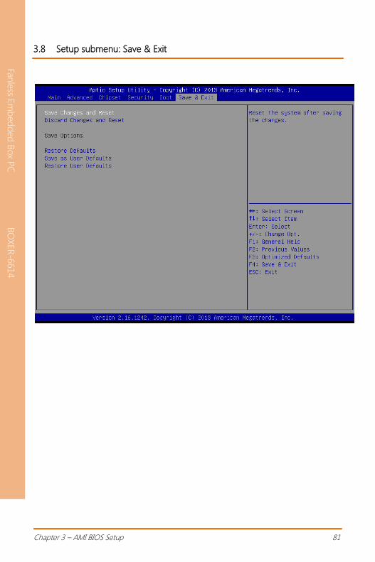
3.8 Setup submenu: Save & Exit

Fanle
ss Em
bed
ded
Box P
C
BO
XER
-6614
Chapter 4
Chapter 4 – Drivers Installation

Chapter 4 – iX Developer 83
Fanle
ss Em
bed
ded
Box P
C
BO
XER
-6614
4.1 Product CD/DVD
The BOXER-6614 comes with a product DVD that contains all the drivers and utilities
you need to setup your product. Insert the DVD and follow the steps in the autorun
program to install the drivers.
In case the program does not start, follow the sequence below to install the drivers.
Step 1 – Install Chipset Driver
1. Open the Step1 - Chipset folder and select your OS
2. Open the SetupChipset.exe file in the folder
3. Follow the instructions
4. Drivers will be installed automatically
Step 2 – Install Graphics Driver
1. Open the Step2 - Graphic folder and select your OS
2. Open the Setup.exe file in the folder
3. Follow the instructions
4. Drivers will be installed automatically
Step 3 – Install LAN Driver
1. Open the Step3 - LAN folder and select your OS
2. Open the .exe file in the folder
3. Follow the instructions
4. Drivers will be installed automatically
Step 4 – Install Audio Driver
1. Open the Step4 - Audio folder and select your OS
Chapter 4 – iX Developer 84
Fanle
ss Em
bed
ded
Box P
C
BO
XER
-6614
2. followed by the .exe file in the folder
3. Follow the instructions
4. Drivers will be installed automatically
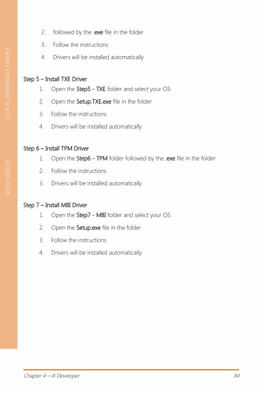
Step 5 – Install TXE Driver
1. Open the Step5 - TXE folder and select your OS
2. Open the Setup.TXE.exe file in the folder
3. Follow the instructions
4. Drivers will be installed automatically
Step 6 – Install TPM Driver
1. Open the Step6 - TPM folder followed by the .exe file in the folder
2. Follow the instructions
3. Drivers will be installed automatically
Step 7 – Install MBI Driver
1. Open the Step7 - MBI folder and select your OS
2. Open the Setup.exe file in the folder
3. Follow the instructions
4. Drivers will be installed automatically
Chapter 4 – iX Developer 85
Fanle
ss Em
bed
ded
Box P
C
BO
XER
-6614
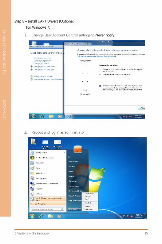
Step 8 – Install UART Drivers (Optional)
For Windows 7:
1. Change User Account Control settings to Never notify
2. Reboot and log in as administrator
Chapter 4 – iX Developer 86
Fanle
ss Em
bed
ded
Box P
C
BO
XER
-6614
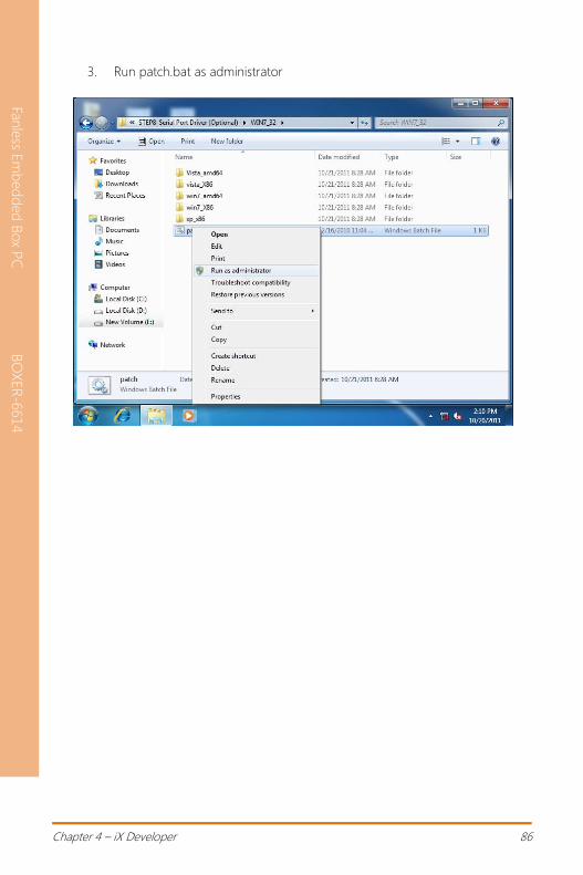
3. Run patch.bat as administrator

Chapter 4 – iX Developer 87
Fanle
ss Em
bed
ded
Box P
C
BO
XER
-6614
For Windows 8:
1. Open the Apps Screen, right click on the Command Prompt tile and select
Run as Administrator
2. To install the driver (patch.bat), you will first have to locate the file in
command prompt. To do that, go to the folder in which the file resides by
entering cd (file path) eg: if the file is in a folder named abc in c drive,
enter cd c:\abc (screenshot for reference only)
3. You are now at the folder where the file is located. Enter the patch.bat to
open and install the drivers.
Chapter 4 – iX Developer 88
Fanle
ss Em
bed
ded
Box P
C
BO
XER
-6614
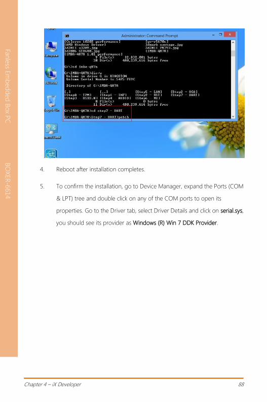
4. Reboot after installation completes.
5. To confirm the installation, go to Device Manager, expand the Ports (COM
& LPT) tree and double click on any of the COM ports to open its
properties. Go to the Driver tab, select Driver Details and click on serial.sys,
you should see its provider as Windows (R) Win 7 DDK Provider.
Chapter 4 – iX Developer 89
Fanle
ss Em
bed
ded
Box P
C
BO
XER
-6614
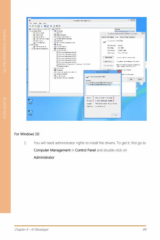
For Windows 10:
1. You will need administrator rights to install the drivers. To get it, first go to
Computer Management in Control Panel and double-click on
Administrator
Chapter 4 – iX Developer 90
Fanle
ss Em
bed
ded
Box P
C
BO
XER
-6614
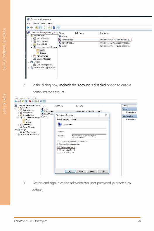
2. In the dialog box, uncheck the Account is disabled option to enable
administrator account.
3. Restart and sign in as the administrator (not password-protected by
default)
Chapter 4 – iX Developer 91
Fanle
ss Em
bed
ded
Box P
C
BO
XER
-6614
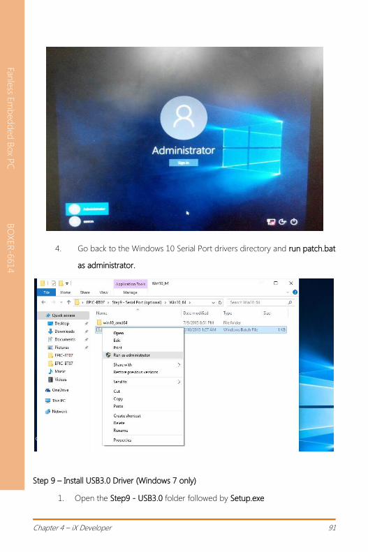
4. Go back to the Windows 10 Serial Port drivers directory and run patch.bat
as administrator.
Step 9 – Install USB3.0 Driver (Windows 7 only)
1. Open the Step9 - USB3.0 folder followed by Setup.exe

Chapter 4 – iX Developer 92
Fanle
ss Em
bed
ded
Box P
C
BO
XER
-6614
2. Follow the instructions
3. Drivers will be installed automatically

Fanle
ss Em
bed
ded
Box P
C
BO
XER
-6614
Appendix A
Appendix A - Watchdog Timer Programming
Appendix A – Watchdog Timer Programming 94
Fanle
ss Em
bed
ded
Box P
C
BO
XER
-6614
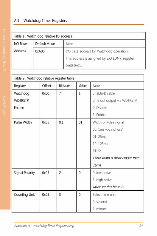
A.1 Watchdog Timer Registers
Table 1 : Watch dog relative IO address
I/O Base
Address
Default Value Note
0xA00 I/O Base address for Watchdog operation.
This address is assigned by SIO LDN7, register
0x60‐0x61.
Table 2 : Watchdog relative register table
Register Offset BitNum Value Note
Watchdog
WDTRST#
Enable
0x00 7 1 Enable/Disable
time out output via WDTRST#
0: Disable
1: Enable
Pulse Width 0x05 0:1 01 Width of Pulse signal
00: 1ms (do not use)
01: 25ms
10: 125ms
11: 5s
Pulse width is must longer than
16ms.
Signal Polarity 0x05 2 0 0: low active
1: high active
Must set this bit to 0
Counting Unit 0x05 3 0 Select time unit.
0: second
1: minute
Appendix A – Watchdog Timer Programming 95
Fanle
ss Em
bed
ded
Box P
C
BO
XER
-6614
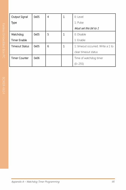
Output Signal
Type
0x05 4 1 0: Level
1: Pulse
Must set this bit to 1
Watchdog
Timer Enable
0x05 5 1 0: Disable
1: Enable
Timeout Status 0x05 6 1 1: timeout occurred. Write a 1 to
clear timeout status
Timer Counter 0x06 Time of watchdog timer
(0~255)
Appendix A – Watchdog Timer Programming 96
Fanle
ss Em
bed
ded
Box P
C
BO
XER
-6614
A.2 Watchdog Sample Program
*********************************************************************// WDT I/O
operation relative definition (Please reference to Table 1)
#define WDTAddr 0xA00 // WDT I/O base address
Void WDTWriteByte(byte Register, byte Value);
byte WDTReadByte(byte Register);
Void WDTSetReg(byte Register, byte Bit, byte Val);
// Watch Dog relative definition (Please reference to Table 2)
#define DevReg 0x00 // Device configuration register
#define WDTRstBit 0x80 // Watchdog WDTRST# (Bit7)
#define WDTRstVal 0x80 // Enabled WDTRST#
#define TimerReg 0x05 // Timer register
#define PSWidthBit 0x00 // WDTRST# Pulse width (Bit0:1)
#define PSWidthVal 0x01 // 25ms for WDTRST# pulse
#define PolarityBit 0x02 // WDTRST# Signal polarity (Bit2)
#define PolarityVal 0x00 // Low active for WDTRST#
#define UnitBit 0x03 // Unit for timer (Bit3)
#define ModeBit 0x04 // WDTRST# mode (Bit4)
#define ModeVal 0x01 // 0:level 1: pulse
#define EnableBit 0x05 // WDT timer enable (Bit5)
#define EnableVal 0x01 // 1: enable
#define StatusBit 0x06 // WDT timer status (Bit6)
#define CounterReg 0x06 // Timer counter register
*********************************************************************
*********************************************************************
VOID Main(){
// Procedure : AaeonWDTConfig
// (byte)Timer : Counter of WDT timer.(0x00~0xFF)
Appendix A – Watchdog Timer Programming 97
Fanle
ss Em
bed
ded
Box P
C
BO
XER
-6614
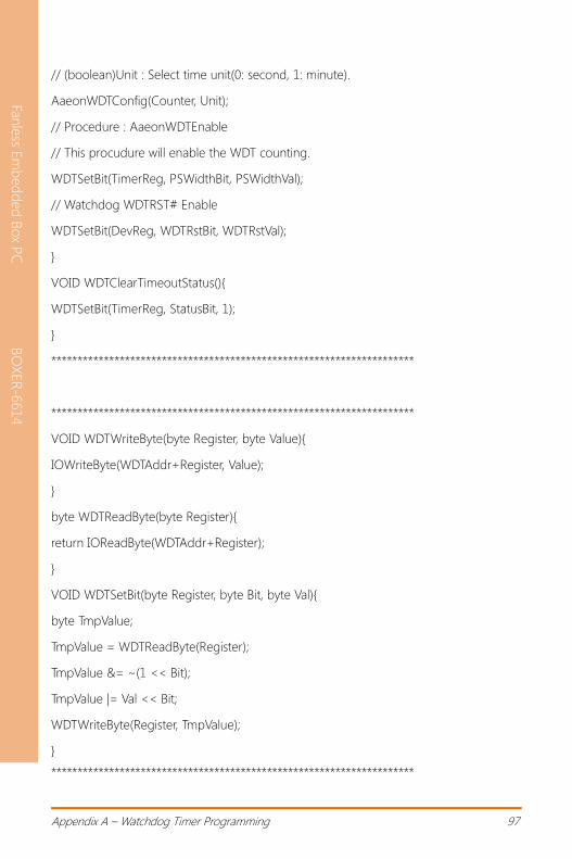
// (boolean)Unit : Select time unit(0: second, 1: minute).
AaeonWDTConfig(Counter, Unit);
// Procedure : AaeonWDTEnable
// This procudure will enable the WDT counting.
WDTSetBit(TimerReg, PSWidthBit, PSWidthVal);
// Watchdog WDTRST# Enable
WDTSetBit(DevReg, WDTRstBit, WDTRstVal);
}
VOID WDTClearTimeoutStatus(){
WDTSetBit(TimerReg, StatusBit, 1);
}
*********************************************************************
*********************************************************************
VOID WDTWriteByte(byte Register, byte Value){
IOWriteByte(WDTAddr+Register, Value);
}
byte WDTReadByte(byte Register){
return IOReadByte(WDTAddr+Register);
}
VOID WDTSetBit(byte Register, byte Bit, byte Val){
byte TmpValue;
TmpValue = WDTReadByte(Register);
TmpValue &= ~(1 << Bit);
TmpValue |= Val << Bit;
WDTWriteByte(Register, TmpValue);
}
*********************************************************************

Fanle
ss Em
bed
ded
Box P
C
BO
XER
-6614
Appendix B
Appendix B - I/O Information
Appendix B – I/O Information 99
Fanle
ss Em
bed
ded
Box P
C
BO
XER
-6614
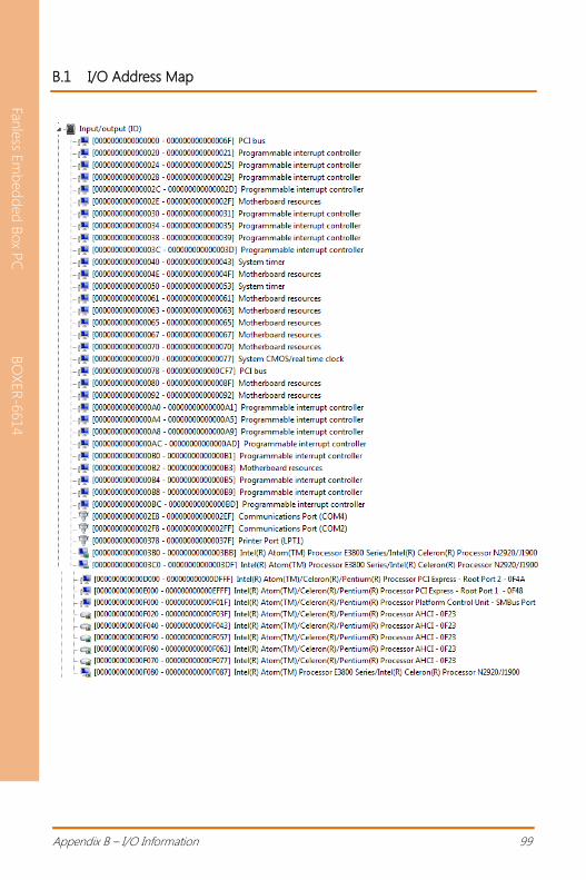
B.1 I/O Address Map

Appendix B – I/O Information 100
Fanle
ss Em
bed
ded
Box P
C
BO
XER
-6614
B.2 Memory Address Map
Appendix B – I/O Information 101
Fanle
ss Em
bed
ded
Box P
C
BO
XER
-6614
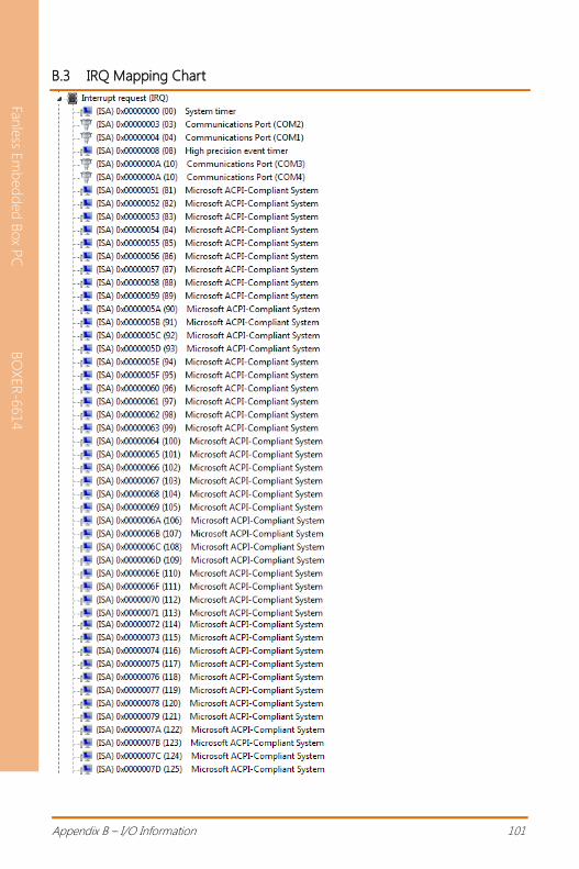
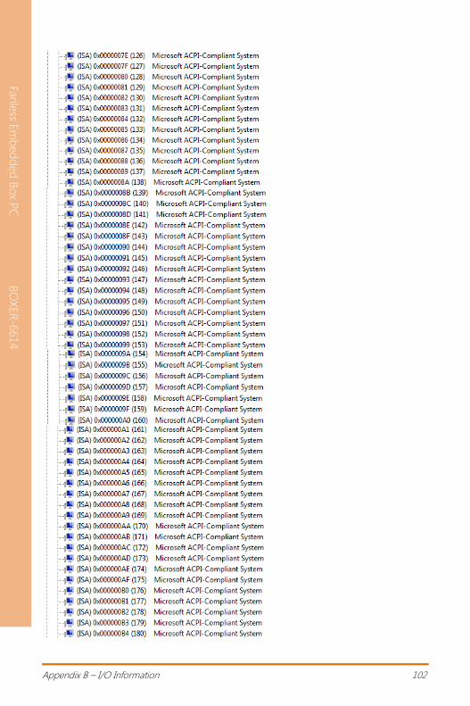
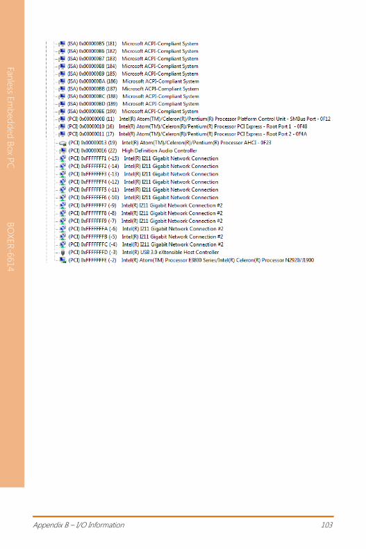
B.3 IRQ Mapping Chart
Appendix B – I/O Information 102
Fanle
ss Em
bed
ded
Box P
C
BO
XER
-6614
Appendix B – I/O Information 103
Fanle
ss Em
bed
ded
Box P
C
BO
XER
-6614
Appendix B – I/O Information 104
Fanle
ss Em
bed
ded
Box P
C
BO
XER
-6614
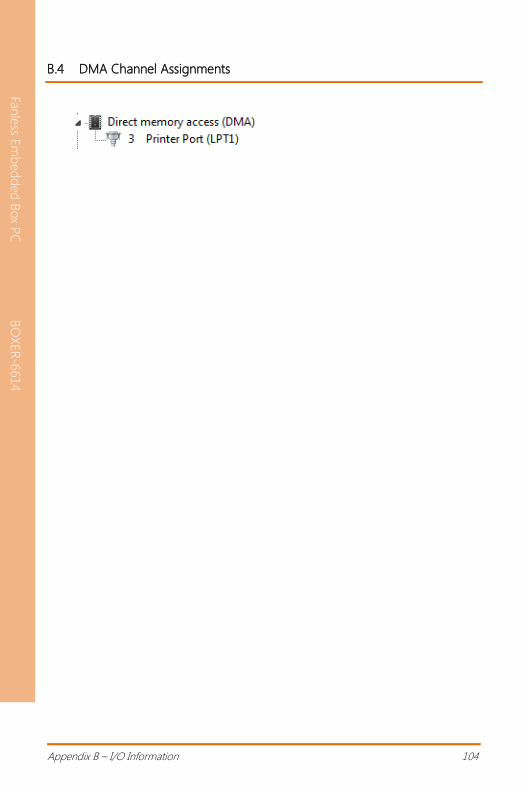
B.4 DMA Channel Assignments