Embed Size (px)
Citation preview
Chapter 3
Combinational Logic Design

March 9, 2009 55:032 - Introduction to Digital Design Page 2
Combinational Logic
One or more digital signal inputs One or more digital signal outputs Outputs are only functions of current input
values (ideal) plus logic propagation delays
Combinational Logic
I1
Im
O1
On
O1 t+Δ t =F1 I1 t , .. . Im t
On t+Δ t =Fn I1 t , .. . I m t
March 9, 2009 55:032 - Introduction to Digital Design Page 3
Combinational Logic (cont.)
Combinational logic has no memory! Outputs are only function of current input
combination Nothing is known about past events Repeating a sequence of inputs always gives the
same output sequence
Sequential logic (covered later) does have memory Repeating a sequence of inputs can result in an
entirely different output sequence
March 9, 2009 55:032 - Introduction to Digital Design Page 4
Design Hierarchy
Large systems are usually too complex to design as a single entity I.e. a 16 bit binary adder has 32 inputs and
therefore there are 232 rows in the truth table!
System is usually partitioned into smaller parts which are further partitioned …
This defines a hierarchy of design from complex to simple; top to bottom

March 9, 2009 55:032 - Introduction to Digital Design Page 5
Design Methodologies
There are two basic approaches to system design Top-Down: start at the top system level and
decompose into ever simpler subsystems and components
Bottom-Up: start with known low-level building blocks and put them together into increasing complex functions
Ideally either should work; in practice neither method does
March 9, 2009 55:032 - Introduction to Digital Design Page 6
Concurrent Design
The practical approach is to combine the two Basic top-down to provide proper decomposition
and validation BUT as you decompose functions, be aware of:
already existing and available components component to component interface characteristics reality - cost, size, weight, power, etc.
If done properly, you end up with a low-cost practical solution that works!
March 9, 2009 55:032 - Introduction to Digital Design Page 7
Rapid Prototyping and CAD
Design verification is much more difficult with VLSI ASICs than with SSI designs Lots more signals and less accessibility
Rapid prototyping assumes we can built many different versions and see which ones work Programmable logic is vital to this approach Good development tools are also essential
Hardware description languages are the way we quickly specify and change our designs
March 9, 2009 55:032 - Introduction to Digital Design Page 8
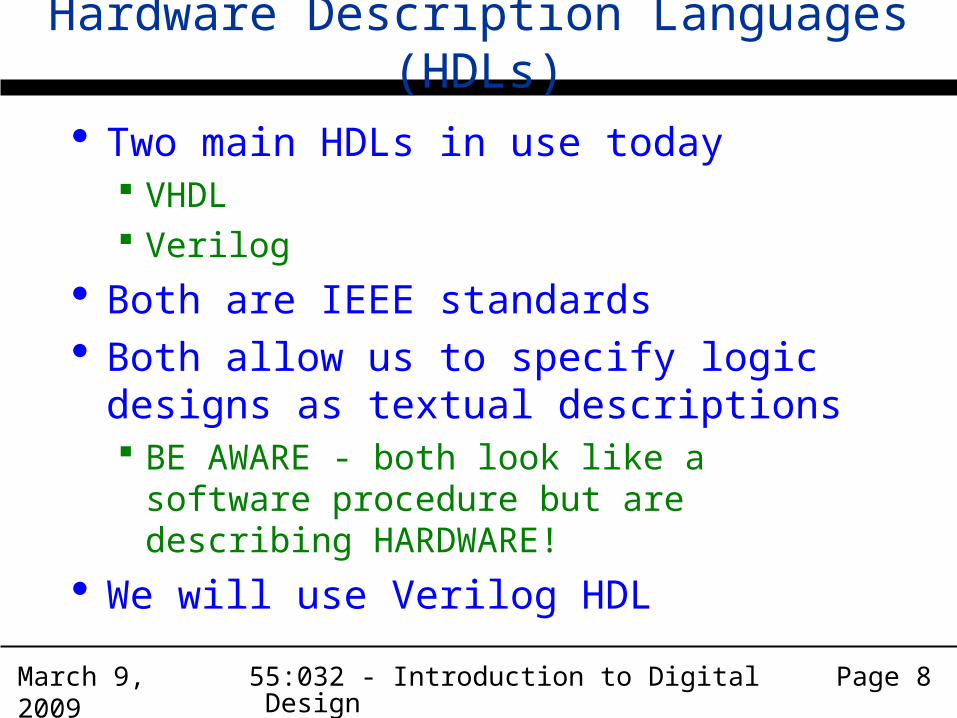
Hardware Description Languages (HDLs)
Two main HDLs in use today VHDL Verilog
Both are IEEE standards Both allow us to specify logic designs as
textual descriptions BE AWARE - both look like a software
procedure but are describing HARDWARE!
We will use Verilog HDL
March 9, 2009 55:032 - Introduction to Digital Design Page 9
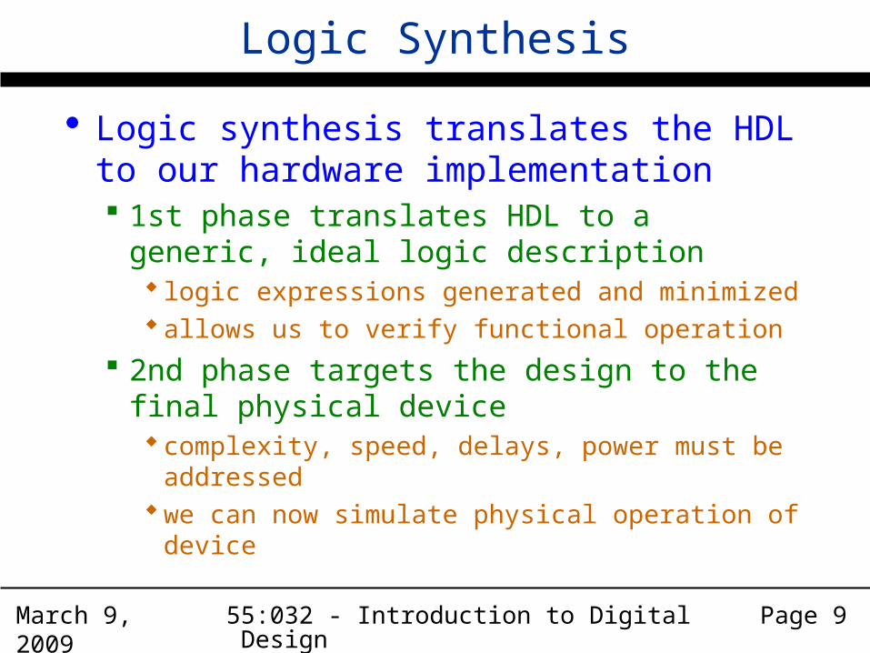
Logic Synthesis
Logic synthesis translates the HDL to our hardware implementation 1st phase translates HDL to a generic, ideal logic
description logic expressions generated and minimized allows us to verify functional operation
2nd phase targets the design to the final physical device complexity, speed, delays, power must be addressedwe can now simulate physical operation of device

March 9, 2009 55:032 - Introduction to Digital Design Page 10
Digital Logic Implementation
Circuit Properties: logic representation, size, weight, power, package, temperature, COST
Levels of Integration: small scale ICs with a few basic gates per package to VLSI devices containing millions of gates per package
Circuit Technology: TTL, ECL, CMOS, GaAs, SiGe, etc.

March 9, 2009 55:032 - Introduction to Digital Design Page 11
Technology Parameters
Fan-in Fan-out Noise margin Propagation delay Power dissipation

March 9, 2009 55:032 - Introduction to Digital Design Page 12
Fan-In
For logic gates, it’s the number of inputs to a specific gate Defined by gate design; usually limited to a max
of 4 or 5 E.G. 74LS08 is a Quad, 2-input AND device
4 AND gates in package, each AND has 2 inputs
Primary impact is when you have more variables than your gate has input Cascade gates, transform function, etc.
March 9, 2009 55:032 - Introduction to Digital Design Page 13
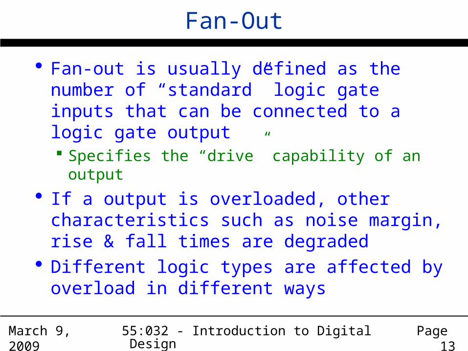
Fan-Out
Fan-out is usually defined as the number of “standard” logic gate inputs that can be connected to a logic gate output Specifies the “drive” capability of an output
If a output is overloaded, other characteristics such as noise margin, rise & fall times are degraded
Different logic types are affected by overload in different ways

March 9, 2009 55:032 - Introduction to Digital Design Page 14
Noise Margin
Noise Margin defines how much noise can be induced onto a logic signal and still be correctly recognized as a high or low level Difference between output high or low level and
input level that will be recognized as high or low
Voh = 2.8 vVih = 2.4 v
Vil = 0.8 vVol = 0.4v
Noise margin high = 0.4 v
Noise margin low = 0.4 v
Transition region; neither Hi or Lo!TTLLogicLevels

March 9, 2009 55:032 - Introduction to Digital Design Page 15
Propagation Delay
Real devices do not have zero delay! Propagation delays are measured from input
change to output change (tPD) Usually referenced to 50% point on transition
Gates usually have different delays for the output low to high (tLH) and high to low (tHL)
Best to design using the max of the two Not all input changes show up at the output
Gate may not respond to a narrow pulse

March 9, 2009 55:032 - Introduction to Digital Design Page 16
Power Dissipation
The quantity of electrical power that is dissipated by the device as heat Devices have temperature operating range that
device cannot exceed
Power dissipation is mainly static or dynamic depending on the logic type TTL/ECL dissipation is mainly static and
therefore independent of signal rate of change CMOS dissipation is mainly dynamic and
increases linearly with increasing signal freq.

March 9, 2009 55:032 - Introduction to Digital Design Page 17
Signal Active States and Bubbles
Primarily applies to control signals; used to denote when a condition is active or enabled Active State - signal state (0 or 1) that indicates
the assertion of some condition or actionAlso called the excitation stateA signal is asserted when it is in the active stateA signal is negated when it is in the inactive stateActive-1 (active high) is when active state is logic 1Active-0 (active low) is when active state is logic 0
Symbol pins without bubbles denote active-1 Symbol pins with bubbles denote active-0
March 9, 2009 55:032 - Introduction to Digital Design Page 18
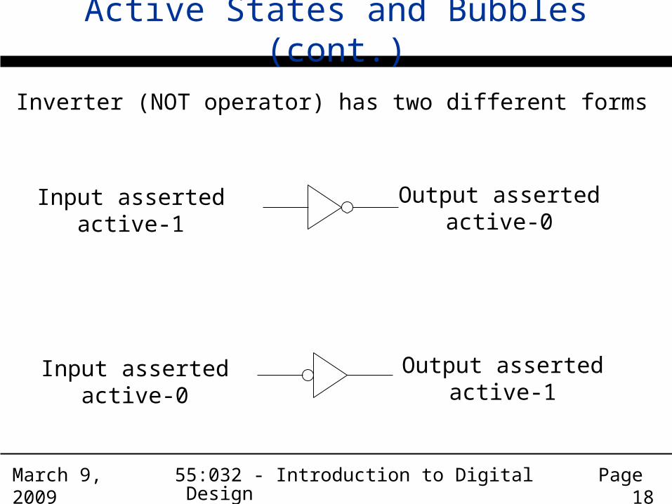
Active States and Bubbles (cont.)
Inverter (NOT operator) has two different forms
Input assertedactive-1
Output assertedactive-0
Input assertedactive-0
Output assertedactive-1

March 9, 2009 55:032 - Introduction to Digital Design Page 19
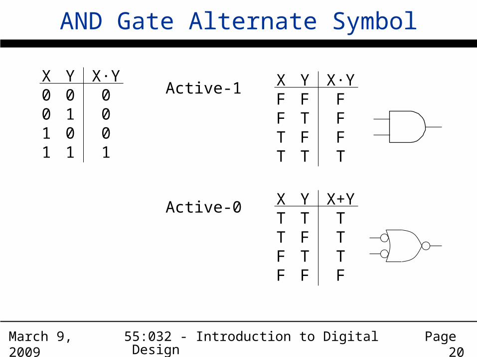
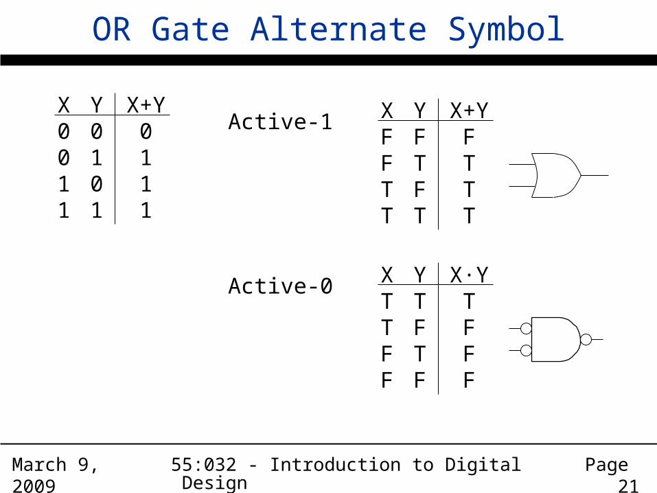
Alternative Symbols
The NOT example can be extended to all logic gates Each logic gate has two equivalent symbols
The one we’ve seen so far for active-1 inputsThe alternate for active-0 inputs
In each case the gate operates the sameThe only difference is how we interpret the values
March 9, 2009 55:032 - Introduction to Digital Design Page 20
AND Gate Alternate Symbol
X0011
Y0101
X·Y0001
XFFTT
YFTFT
X·YFFFT
XTTFF
YTFTF
X+YTTTF
Active-1
Active-0
March 9, 2009 55:032 - Introduction to Digital Design Page 21
OR Gate Alternate Symbol
X0011
Y0101
X+Y0111
XFFTT
YFTFT
X+YFTTT
XTTFF
YTFTF
X·YTFFF
Active-1
Active-0

March 9, 2009 55:032 - Introduction to Digital Design Page 22
Other Gate Alternative Symbols
NAND
NOR
XOR
XNOR
Active-1 Active-0

March 9, 2009 55:032 - Introduction to Digital Design Page 23
Signal Naming Conventions
The problem is how to distinguish between active-1 and active-0 signals. Barring a signal name to designate active-0 is
not recommended Is A active-0 or NOT A??
Use suffix of ‘_0’; (i.e A_0) after signal name Use suffix of ‘_LO’ or ‘_L’ Use suffix of ‘_BAR’
No matter what you use, BE CONSISTENT!
A

March 9, 2009 55:032 - Introduction to Digital Design Page 24
Signal Naming (cont.)
Active-0 signal naming and symbol bubbles require some thought to interpret properly
A_L(active-0)
A(active-1)
A_L(active-0)
A(active-1)

March 9, 2009 55:032 - Introduction to Digital Design Page 25
Naming and Alternate Symbols
Proper active-0 signal naming and usage of alternate symbols can clarify the circuit intent
HEATTEMP1_LTEMP2_L
HEAT = TEMP1_L ⋅ TEMP2_L
This is really a NOR gate
TEMP1_L
TEMP2_LHEAT
TEMP1
TEMP2

March 9, 2009 55:032 - Introduction to Digital Design Page 26
Design Methodology
We start with some form of a problem statement Usually just text; ambiguous, poorly stated
We must produce a design representation S.A. expressions, minimized
The primary problem we have is first to concisely define the true problem we are to solve Define the “system” requirements

March 9, 2009 55:032 - Introduction to Digital Design Page 27
Design Methodology (cont.)
Step 1) - Break down the problem statement Identify system inputs and outputs Extract the stated input-output relationship(s) State the above as system (black-box) level
requirements. BE PRECISE!
Step 2) - Perform initial system definition Define interface variables and representation
If representation is not defined in problem statement, make preliminary assignment
Restate I/O relationship as algorithm, equation, simulation, etc.
March 9, 2009 55:032 - Introduction to Digital Design Page 28
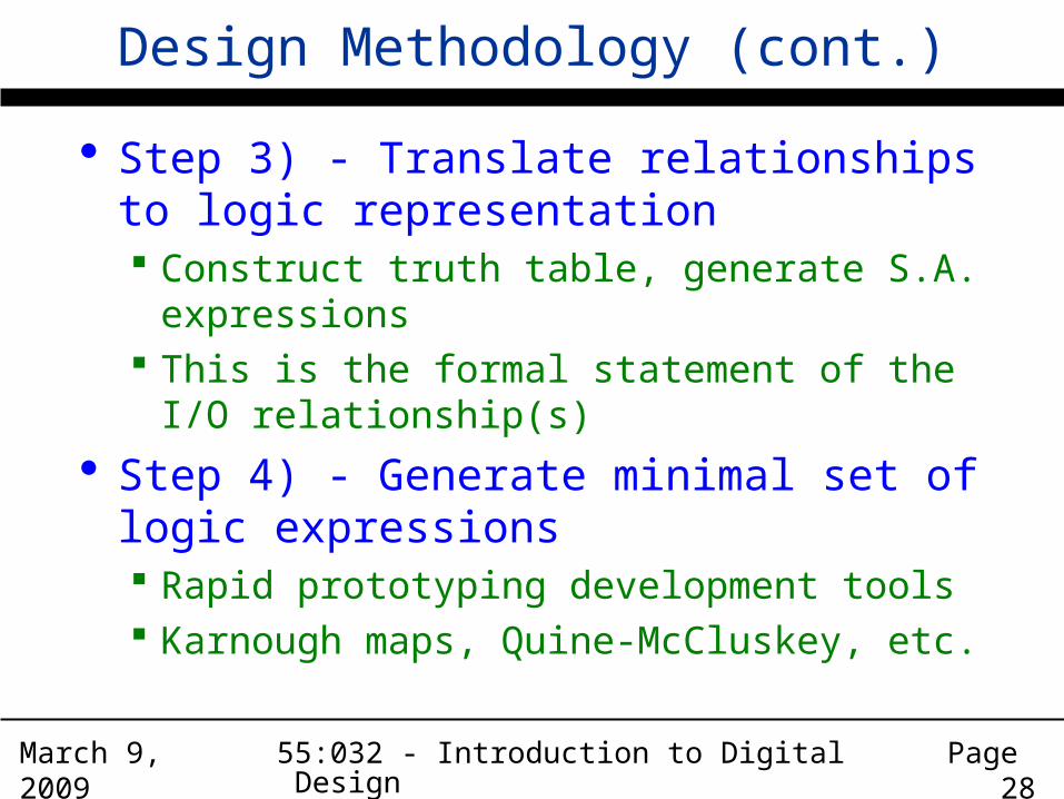
Design Methodology (cont.)
Step 3) - Translate relationships to logic representation Construct truth table, generate S.A. expressions This is the formal statement of the I/O
relationship(s)
Step 4) - Generate minimal set of logic expressions Rapid prototyping development tools Karnough maps, Quine-McCluskey, etc.
March 9, 2009 55:032 - Introduction to Digital Design Page 29
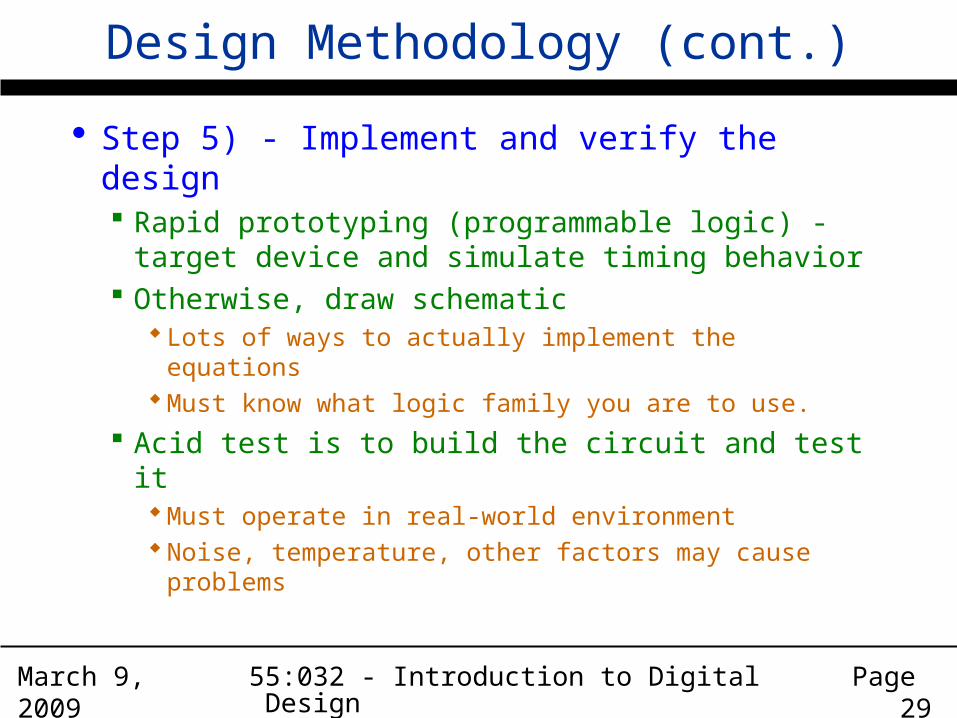
Design Methodology (cont.)
Step 5) - Implement and verify the design Rapid prototyping (programmable logic) - target
device and simulate timing behavior Otherwise, draw schematic
Lots of ways to actually implement the equationsMust know what logic family you are to use.
Acid test is to build the circuit and test itMust operate in real-world environmentNoise, temperature, other factors may cause problems

March 9, 2009 55:032 - Introduction to Digital Design Page 30
BCD to XS3 Example
Initial Statement: “Design a circuit to convert BCD to XS3.” 1) We need to restate and translate this to
specific requirementsR1: The circuit shall input one BCD digitR2: The circuit shall output one XS3 digitR3: The XS3 output shall be the equivalent decimal
value as the BCD input value
XS3(X) <= BCD(X)BCDdigit
XS3digit
March 9, 2009 55:032 - Introduction to Digital Design Page 31
BCD to XS3 Example (cont.)
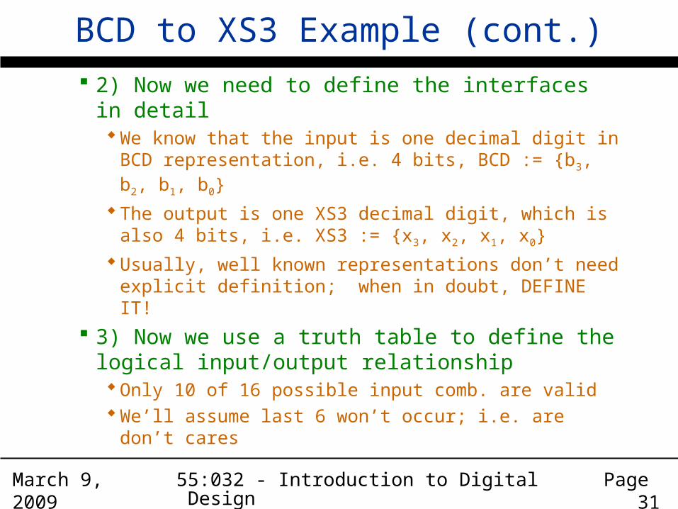
2) Now we need to define the interfaces in detailWe know that the input is one decimal digit in BCD
representation, i.e. 4 bits, BCD := {b3, b2, b1, b0}
The output is one XS3 decimal digit, which is also 4 bits, i.e. XS3 := {x3, x2, x1, x0}
Usually, well known representations don’t need explicit definition; when in doubt, DEFINE IT!
3) Now we use a truth table to define the logical input/output relationshipOnly 10 of 16 possible input comb. are validWe’ll assume last 6 won’t occur; i.e. are don’t cares

March 9, 2009 55:032 - Introduction to Digital Design Page 32
BCD to XS3 Example (cont.)
b0
0101010101010101
b1
0011001100110011
b2
0000111100001111
b3
0000000011111111
x0
1010101010------
x1
1001100110------
x2
0111100001------
x3
0000011111------
Note: Don’t carescan work to our advantage duringminimization; wecan assign either0 or 1 as needed.
March 9, 2009 55:032 - Introduction to Digital Design Page 33
BCD to XS3 Example (cont.)
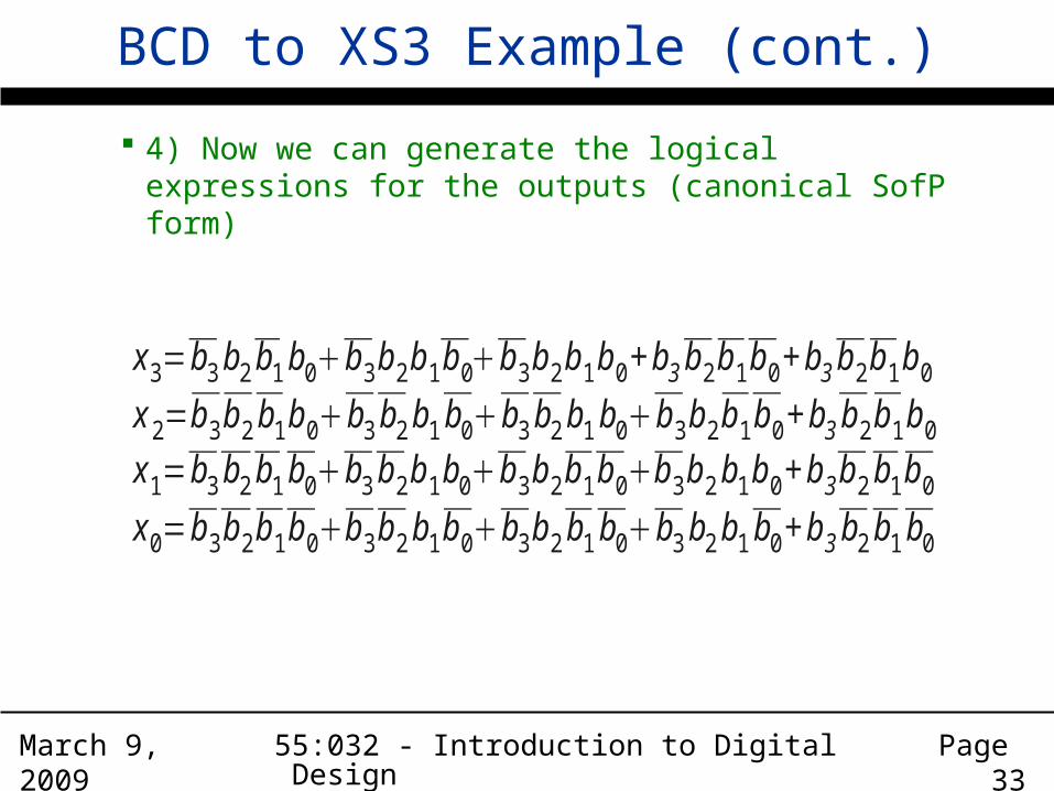
4) Now we can generate the logical expressions for the outputs (canonical SofP form)
x3=b3 b2 b1 b0b3 b2 b1 b0b3 b2 b1 b0 +b3 b2 b1 b0 +b3 b2 b1 b0
x 2=b3 b2 b1 b0b3 b2 b1 b0b3 b2 b1 b0b3 b2 b1 b0 +b3 b2 b1 b0
x1=b3 b2 b1 b0b3 b2 b1 b0b3 b2 b1 b0b3 b2 b1 b0 +b3 b2 b1 b0
x0=b3 b2 b1 b0b3 b2 b1 b0b3 b2 b1 b0b3 b2 b1 b0 +b3 b2 b1 b0

March 9, 2009 55:032 - Introduction to Digital Design Page 34
BCD to XS3 Example (cont.)
The minimized equations are as follows
x3=b3+b2b1+b2b0
x 2=b2 b1b2 b0+b2 b1b0
x1=b1b0+b1 b0=b1 b⊕ 0
x0=b0

March 9, 2009 55:032 - Introduction to Digital Design Page 35
BCD to XS3 Example (cont.)
b0b1
b2
b3
x3
x2
x1
x0
March 9, 2009 55:032 - Introduction to Digital Design Page 36
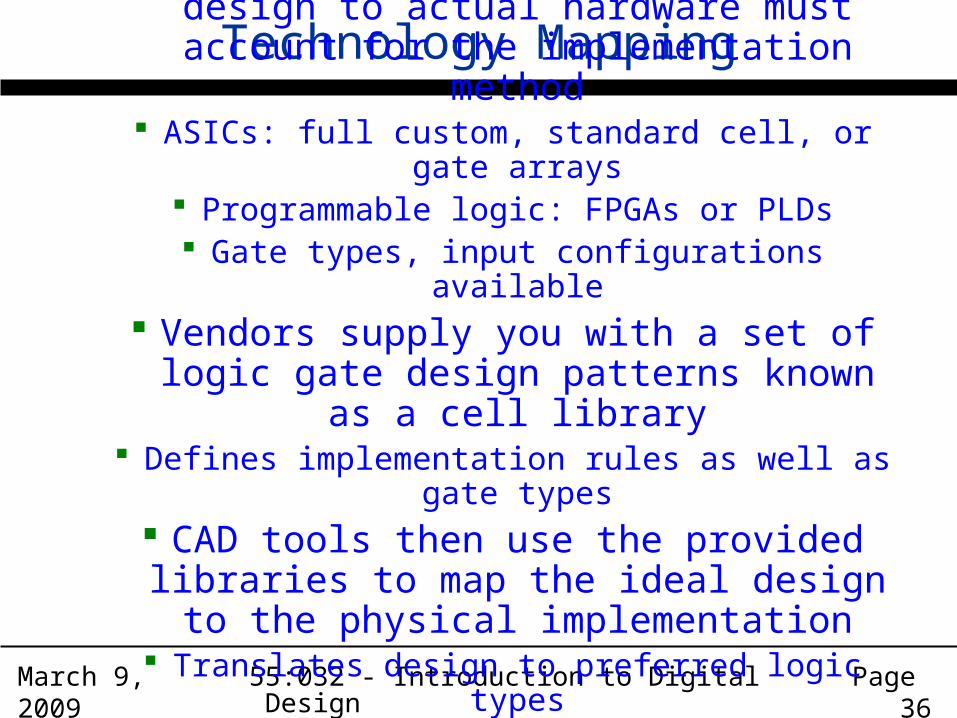
Technology Mapping Translation of “ideal” circuit design to actual hardware must account for the implementation
method ASICs: full custom, standard cell, or gate arrays
Programmable logic: FPGAs or PLDs Gate types, input configurations available
Vendors supply you with a set of logic gate design patterns known as a cell library
Defines implementation rules as well as gate types CAD tools then use the provided libraries to map
the ideal design to the physical implementation Translates design to preferred logic types
Checks for problems; fan-out, propagation times exceeded

March 9, 2009 55:032 - Introduction to Digital Design Page 37
Verification
Ensuring that the final device actually works is mandatory and can also be hard to do Must start with good requirements (validation)
It’s really bad to find out your design meets the stated requirements but it’s not what the customer wanted
Done at different stages of the developmentSimulation used during the design capture and
implementation mapping phaseFunctional and parametric testing after device
fabrication