Embed Size (px)
Citation preview

Chapter 5Combinational Logic Analysis
ETEC 2301 Programmable Logic Devices
Shawnee State UniversityDepartment of Industrial and Engineering Technologies
Copyright © 2007 by Janna B. Gallaher

Basic Combinational Logic Circuits We know that we can create a logic expression using SOP and POS
expressions that use AND and OR gates to implement Now we want to explore the logic functions in more detail AND-OR Logic
− Used to implement SOP expressions
Input s Output
A B C D AB CD X
0 0 0 0 0 0 0
0 0 0 1 0 0 0
0 0 1 0 0 0 0
0 0 1 1 0 1 1
0 1 0 0 0 0 0
0 1 0 1 0 0 0
0 1 1 0 0 0 0
0 1 1 1 0 1 1
1 0 0 0 0 0 0
1 0 0 1 0 0 0
1 0 1 0 0 0 0
1 0 1 1 0 1 1
1 1 0 0 1 0 1
1 1 0 1 1 0 1
1 1 1 0 1 0 1
1 1 1 1 1 1 1
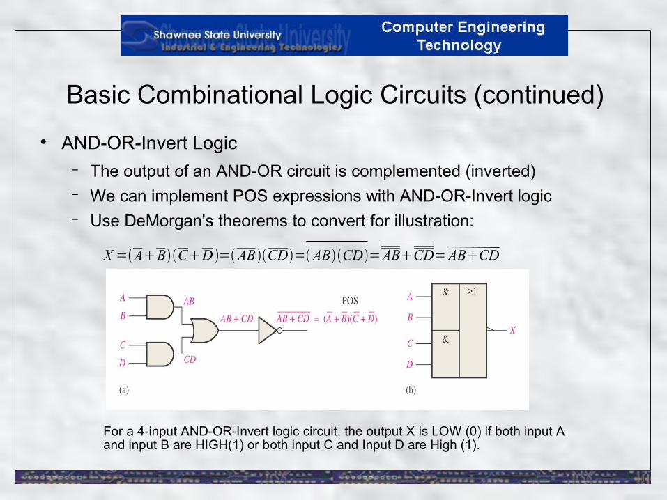
AND-OR-Invert Logic− The output of an AND-OR circuit is complemented (inverted)− We can implement POS expressions with AND-OR-Invert logic− Use DeMorgan's theorems to convert for illustration:
Basic Combinational Logic Circuits (continued)
X=ABCD =ABCD=ABCD=ABCD=ABCD
For a 4-input AND-OR-Invert logic circuit, the output X is LOW (0) if both input A and input B are HIGH(1) or both input C and Input D are High (1).

Exclusive-OR Logic
Basic Combinational Logic Circuits (continued)
Exclusive-NOR Logic
A B X
0 0 0
0 1 1
1 0 1
1 1 0
A B X
0 0 1
0 1 0
1 0 0
1 1 1
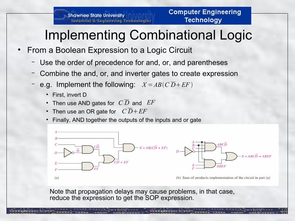
Implementing Combinational Logic From a Boolean Expression to a Logic Circuit
− Use the order of precedence for and, or, and parentheses− Combine the and, or, and inverter gates to create expression− e.g. Implement the following:
First, invert D Then use AND gates for and Then use an OR gate for Finally, AND together the outputs of the inputs and or gate
X=ABC DEF
Note that propagation delays may cause problems, in that case, reduce the expression to get the SOP expression.
C DC DEF
EF

Inputs Output
A B C X Product Term
0 0 0 0
0 0 1 0
0 1 0 0
0 1 1 1 A B C1 0 0 1 A BC1 0 1 0
1 1 0 0
1 1 1 0
Implementing Combinational Logic From a Truth Table to a Logic Circuit
− Create the product term from the truth table− OR together the product terms to get expression
X=A BCA BC

The Universal Property of NAND and NOR Gates The NAND Gate as a Universal Logic Element
Note that we use the NAND gate to create any of the primitive operations.We may want to do this to minimize the number of different types of logic ICs on a circuit board.

The Universal Property of NAND and NOR Gates The NOR Gate as a Universal Logic Element

Combinational Logic Using NAND and NOR Gates NAND Logic
− Using DeMorgan's theorems to show how to create an SOP expression from three NAND gates.
X =AB CDX=ABCDX=ABCD
DeMorganDouble NOT
X=AB CD
Use the bubble notation as a handy way to do DeMorgan's Theorems

Combinational Logic Using NAND and NOR Gates Use of Appropriate Dual Symbols in NAND Logic Diagram
Red arrows indicate use of the DeMorgan equivalent gate.

Combinational Logic Using NAND and NOR Gates NOR Logic
− The NOR gate can create POS expression:
X=AB CDX=ABCD X=ABCD
X=ABCD
De Morgan
Reduce expression using DeMorgan's Theorems
AB
CD

Logic Circuit Operation With Pulse Waveform Inputs We can represent each stage in a logic circuit as a response to a waveform
input:
Y=BC
Y is 1 when either B or C is 1X is 0 when both Y and A are 1

Combinational Logic with VHDL Structural Approach to VHDL Programming
− We can define new logic functions to use as blocks in creating VHDL definitions.
− In our labs we do this by including a schematic as a part of the new design and create a symbol for it
− In VHDL you can use a software approach to define these complex blocks.
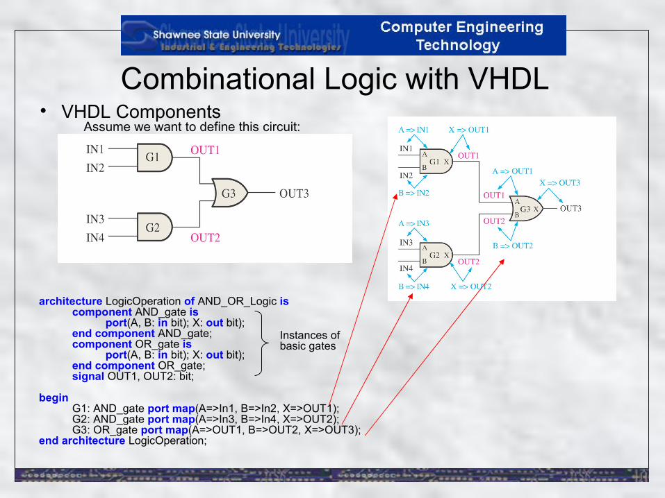
Combinational Logic with VHDL VHDL Components
architecture LogicOperation of AND_OR_Logic iscomponent AND_gate is
port(A, B: in bit); X: out bit);end component AND_gate;component OR_gate is
port(A, B: in bit); X: out bit);end component OR_gate;signal OUT1, OUT2: bit;
beginG1: AND_gate port map(A=>In1, B=>In2, X=>OUT1);G2: AND_gate port map(A=>In3, B=>In4, X=>OUT2);G3: OR_gate port map(A=>OUT1, B=>OUT2, X=>OUT3);
end architecture LogicOperation;
Assume we want to define this circuit:
Instances ofbasic gates
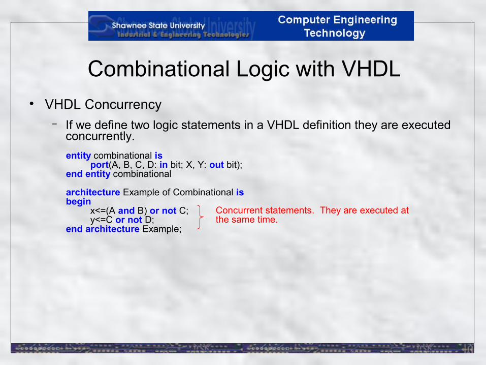
Combinational Logic with VHDL VHDL Concurrency
− If we define two logic statements in a VHDL definition they are executed concurrently.entity combinational is
port(A, B, C, D: in bit; X, Y: out bit);end entity combinational
architecture Example of Combinational isbegin
x<=(A and B) or not C;y<=C or not D;
end architecture Example;
Concurrent statements. They are executed at the same time.

Combinational Logic with VHDL Applying Software Development Tools
Screen shot of Xilinx IDE for a project with module definitions from Lab 7
Project schematic
Module schematic