Embed Size (px)
Citation preview
Communication Systems, 5e
Chapter 7: Analog Communication Systems
A. Bruce CarlsonPaul B. Crilly
© 2010 The McGraw-Hill Companies
Chapter 7: Analog Communication Systems
• Receiver block diagram design• Image frequency bands that may cause
spurious responses (more filter requirements)• Signal Multiplexing
– Frequency division (FDM) and – Time division (TDM)
• Phase-Lock Loops (PLL)
© 2010 The McGraw-Hill Companies
3
Multiplexing
• Combining multiple signals into a wider bandwidth system for transmission– Typically multiplex in time or frequency
• TDM time division multiplexing• FDM frequency division multiplexing
– For time multiplexing, “PAM sampling”, bandwidth based on PAM pulse periods
– For frequency multiplexing, bandwidth is the sum of all the multiplexed elements plus their guard bands
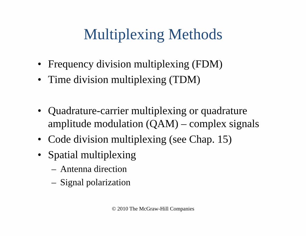
Multiplexing Methods
• Frequency division multiplexing (FDM)• Time division multiplexing (TDM)
• Quadrature-carrier multiplexing or quadrature amplitude modulation (QAM) – complex signals
• Code division multiplexing (see Chap. 15)• Spatial multiplexing
– Antenna direction– Signal polarization
© 2010 The McGraw-Hill Companies
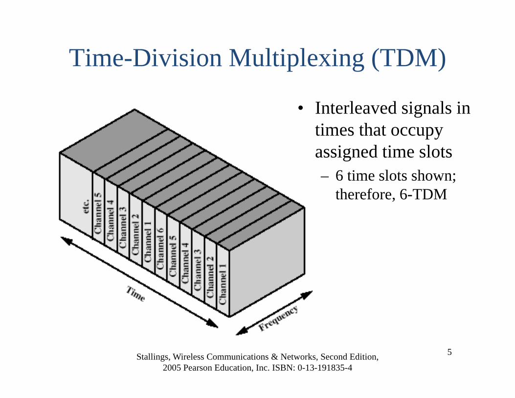
Time-Division Multiplexing (TDM)
5Stallings, Wireless Communications & Networks, Second Edition, 2005 Pearson Education, Inc. ISBN: 0-13-191835-4
• Interleaved signals in times that occupy assigned time slots– 6 time slots shown;
therefore, 6-TDM
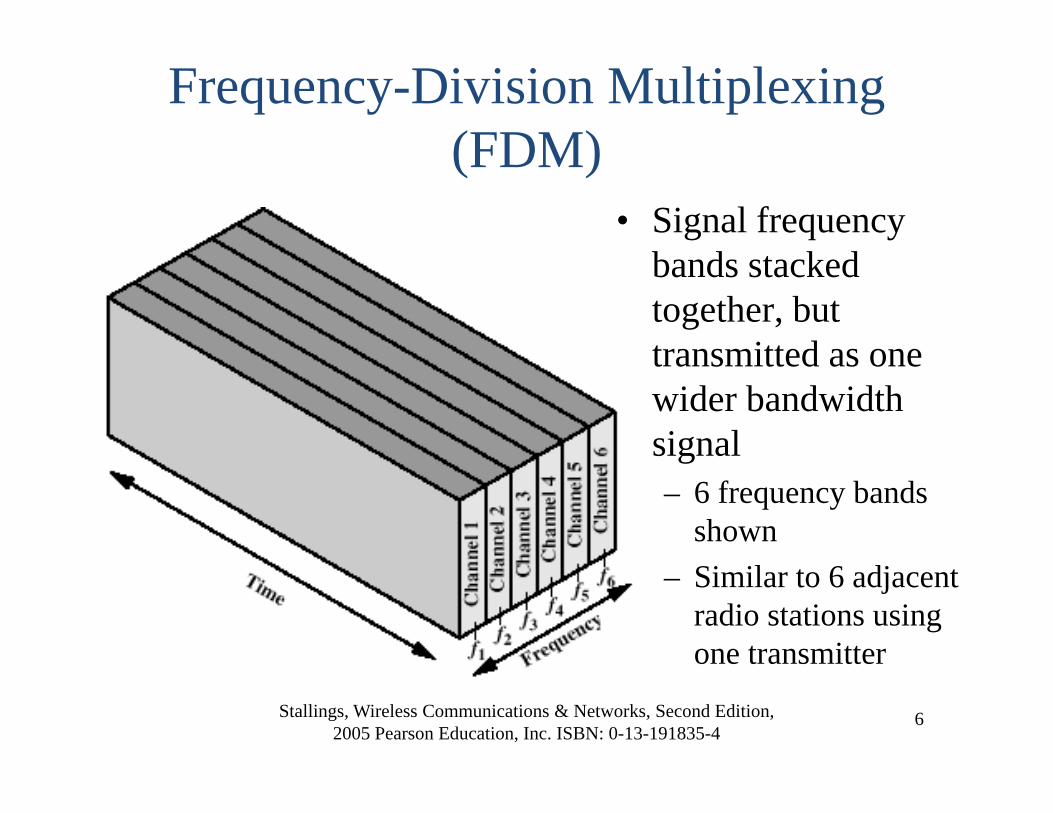
Frequency-Division Multiplexing (FDM)
6Stallings, Wireless Communications & Networks, Second Edition, 2005 Pearson Education, Inc. ISBN: 0-13-191835-4
• Signal frequency bands stacked together, but transmitted as one wider bandwidth signal– 6 frequency bands
shown– Similar to 6 adjacent
radio stations using one transmitter
7
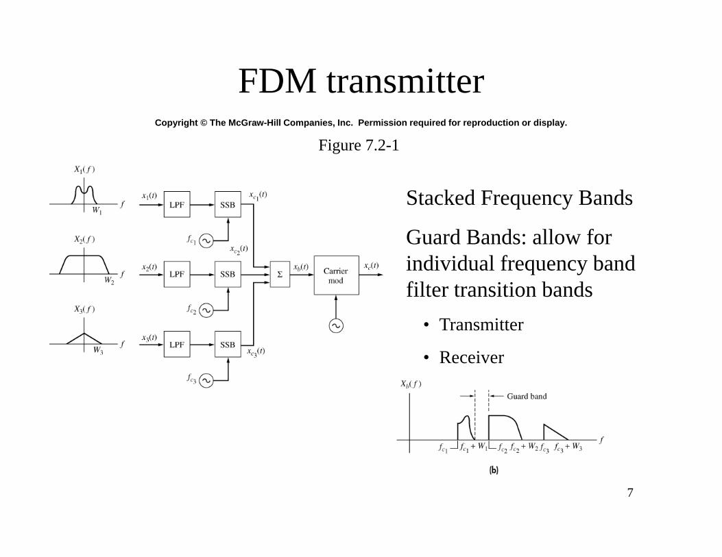
Copyright © The McGraw-Hill Companies, Inc. Permission required for reproduction or display.
Figure 7.2-1
FDM transmitter
Stacked Frequency Bands
Guard Bands: allow for individual frequency band filter transition bands
• Transmitter
• Receiver
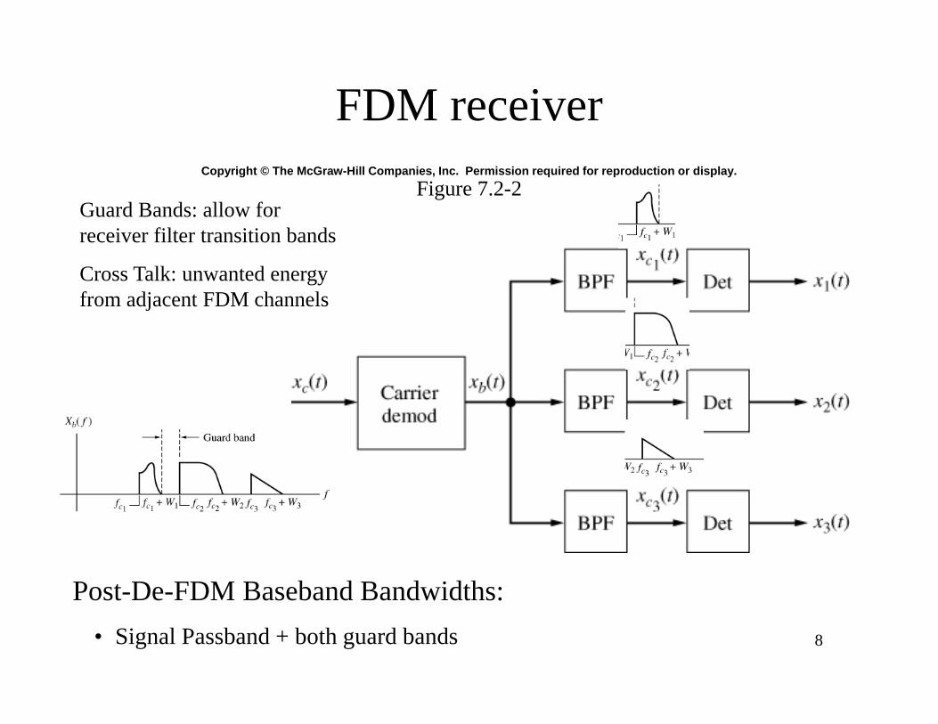
8
Copyright © The McGraw-Hill Companies, Inc. Permission required for reproduction or display.Figure 7.2-2
FDM receiver
Guard Bands: allow for receiver filter transition bands
Cross Talk: unwanted energy from adjacent FDM channels
Post-De-FDM Baseband Bandwidths:• Signal Passband + both guard bands
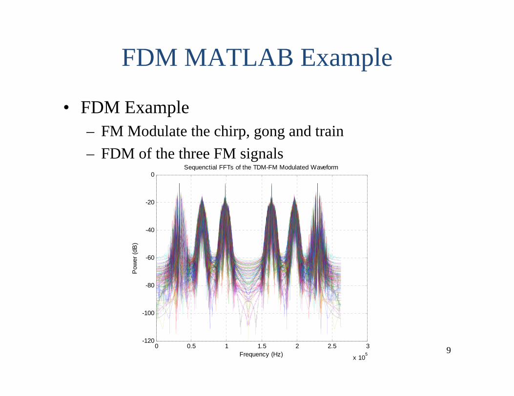
FDM MATLAB Example
• FDM Example– FM Modulate the chirp, gong and train– FDM of the three FM signals
90 0.5 1 1.5 2 2.5 3
x 105
-120
-100
-80
-60
-40
-20
0Sequenctial FFTs of the TDM-FM Modulated Waveform
Frequency (Hz)
Pow
er (d
B)

10
Copyright © The McGraw-Hill Companies, Inc. Permission required for reproduction or display.Figure 7.2-3
FDMA satellite repeater system
Nominal 36 MHz BW Links• 1200 Voice Channels or• 400 channels of 64 kbps or• 16 channels of 1.544 Mbps each or• One 50 Mbps data stream
11
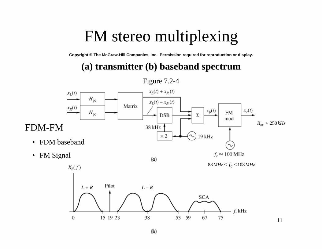
Copyright © The McGraw-Hill Companies, Inc. Permission required for reproduction or display.
(a) transmitter (b) baseband spectrumFigure 7.2-4
FM stereo multiplexing
FDM-FM• FDM baseband
• FM Signal
kHzBRF 250
MHzfMHz C 10888
12
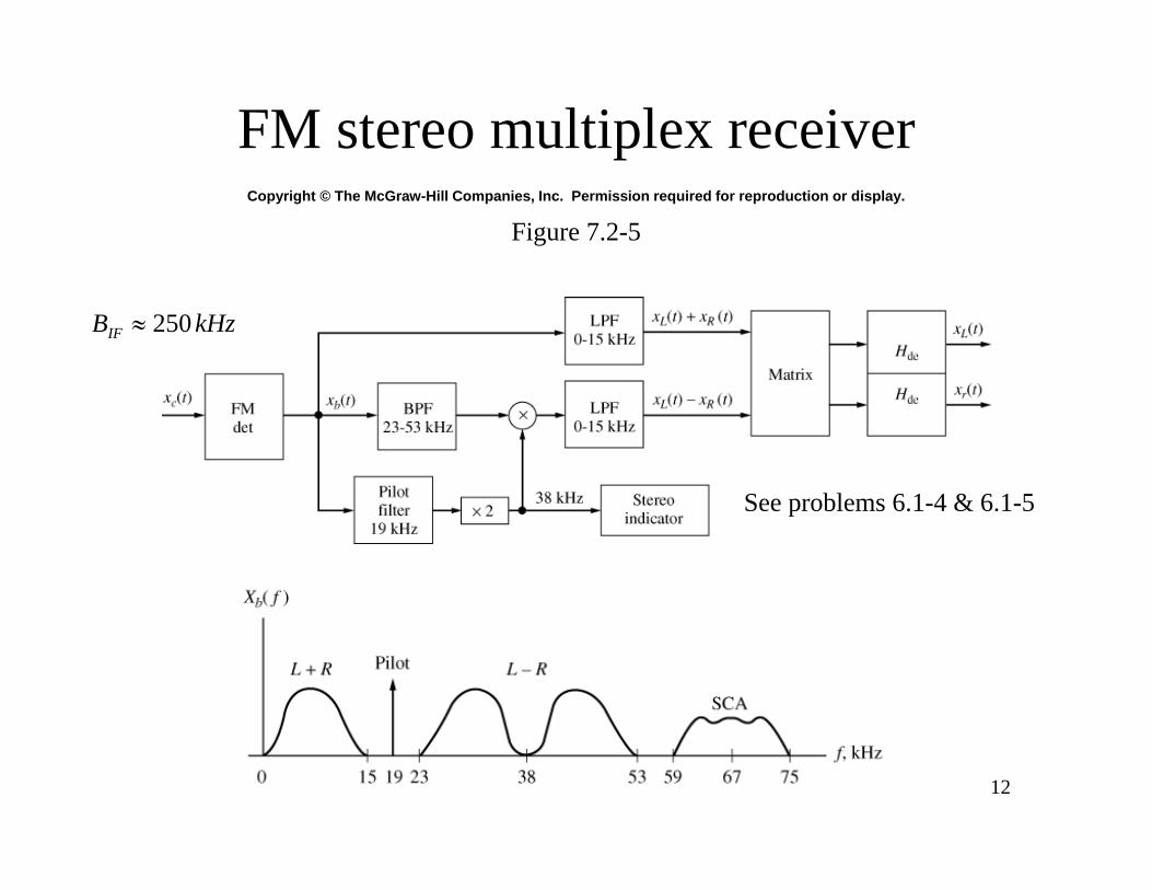
Copyright © The McGraw-Hill Companies, Inc. Permission required for reproduction or display.
Figure 7.2-5
FM stereo multiplex receiver
See problems 6.1-4 & 6.1-5
kHzBIF 250
13
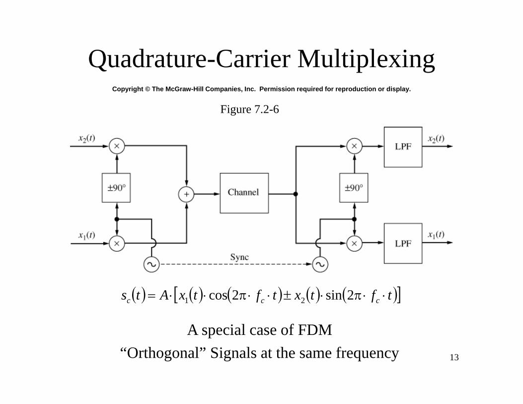
Copyright © The McGraw-Hill Companies, Inc. Permission required for reproduction or display.
Figure 7.2-6
Quadrature-Carrier Multiplexing
tftxtftxAts ccc 2sin2cos 21
A special case of FDM“Orthogonal” Signals at the same frequency
14
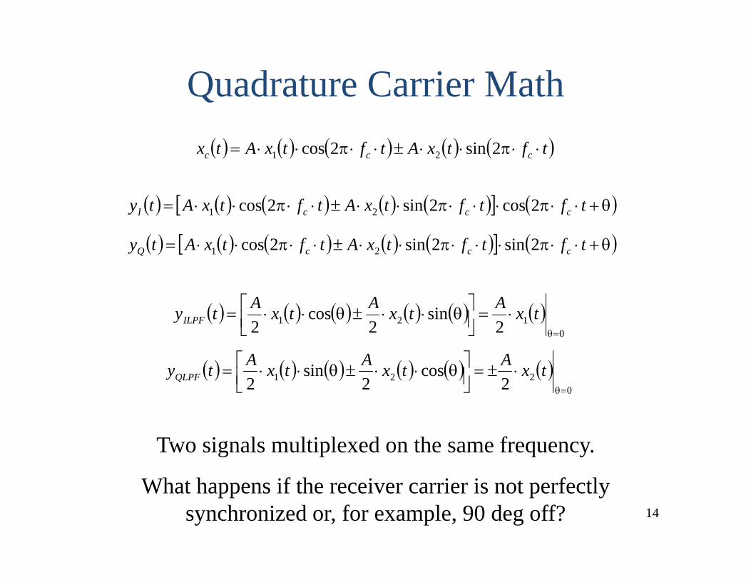
Quadrature Carrier Math
tftftxAtftxAty cccI 2cos2sin2cos 21
tftxAtftxAtx ccc 2sin2cos 21
tftftxAtftxAty cccQ 2sin2sin2cos 21
0
121 2sin
2cos
2
txAtxAtxAtyILPF
0
221 2cos
2sin
2
txAtxAtxAtyQLPF
Two signals multiplexed on the same frequency.
What happens if the receiver carrier is not perfectly synchronized or, for example, 90 deg off?
15
Quadrature FDM Channels
• Each of the frequency bands or channels may have signal that are in quadrature. – Doubling the channel capacity– Phase synchronization of the receiver with the received
waveform is required!
– A precursor to Orthogonal Frequency Division Multiplexing (OFDM)

Time-Division Multiplexing (TDM)
16Stallings, Wireless Communications & Networks, Second Edition, 2005 Pearson Education, Inc. ISBN: 0-13-191835-4
• Interleaved signals in times that occupy assigned time slots– 6 time slots shown;
therefore, 6-TDM
17
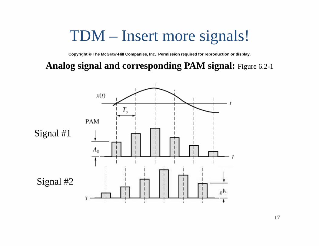
Copyright © The McGraw-Hill Companies, Inc. Permission required for reproduction or display.
Analog signal and corresponding PAM signal: Figure 6.2-1
TDM – Insert more signals!
Signal #1
Signal #2
18
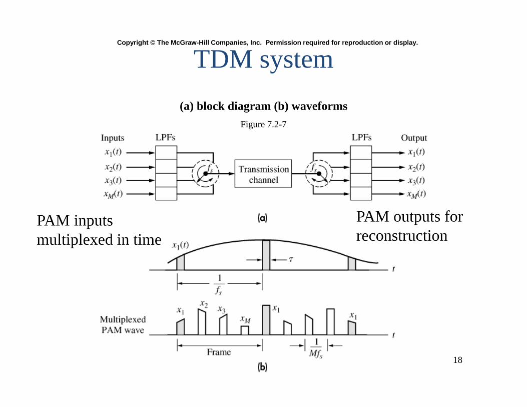
Copyright © The McGraw-Hill Companies, Inc. Permission required for reproduction or display.
(a) block diagram (b) waveformsFigure 7.2-7
TDM system
PAM inputs multiplexed in time
PAM outputs for reconstruction
19
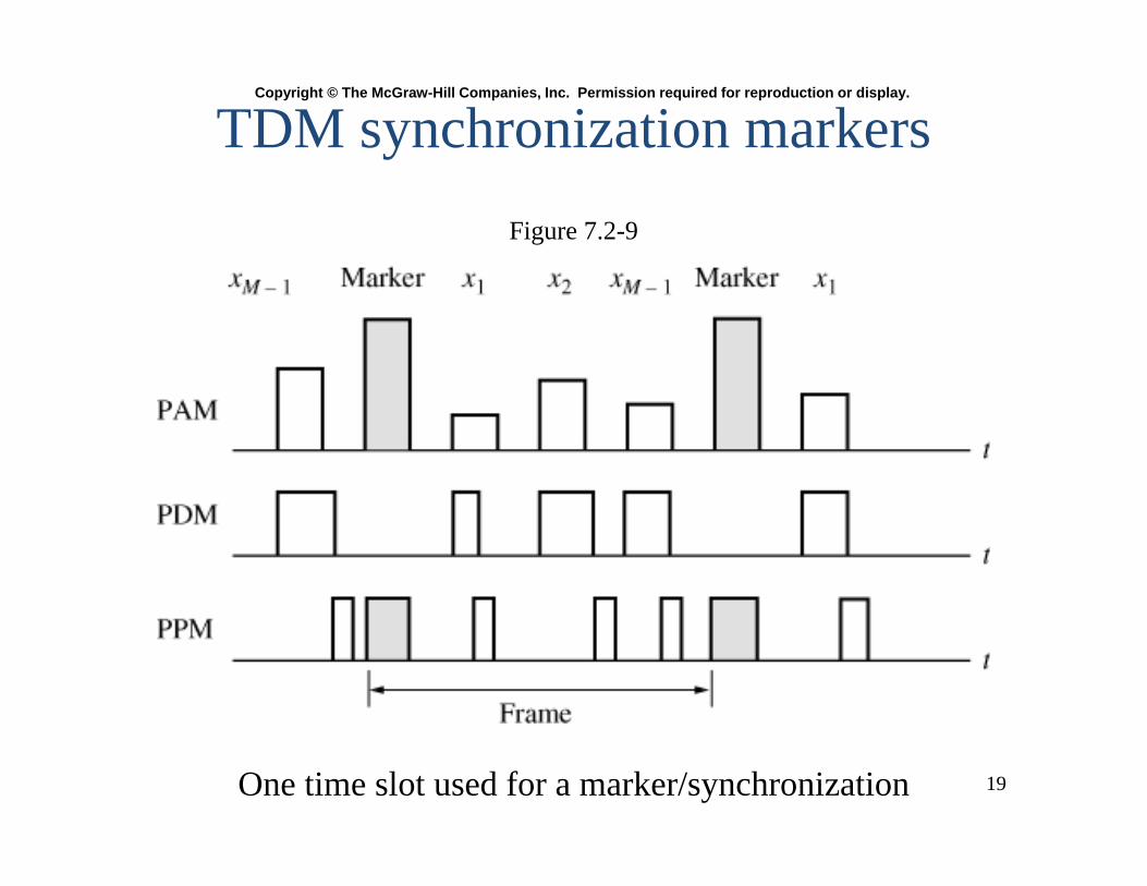
Copyright © The McGraw-Hill Companies, Inc. Permission required for reproduction or display.
Figure 7.2-9
TDM synchronization markers
One time slot used for a marker/synchronization
20
Copyright © The McGraw-Hill Companies, Inc. Permission required for reproduction or display.
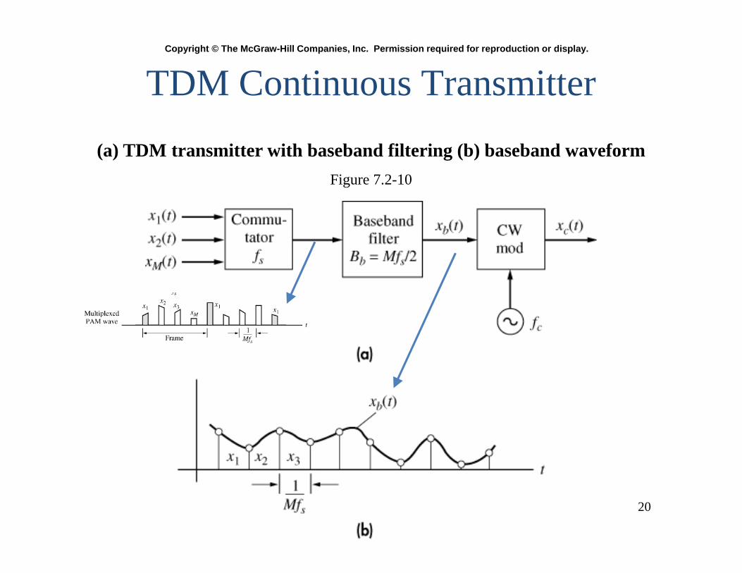
(a) TDM transmitter with baseband filtering (b) baseband waveformFigure 7.2-10
TDM Continuous Transmitter
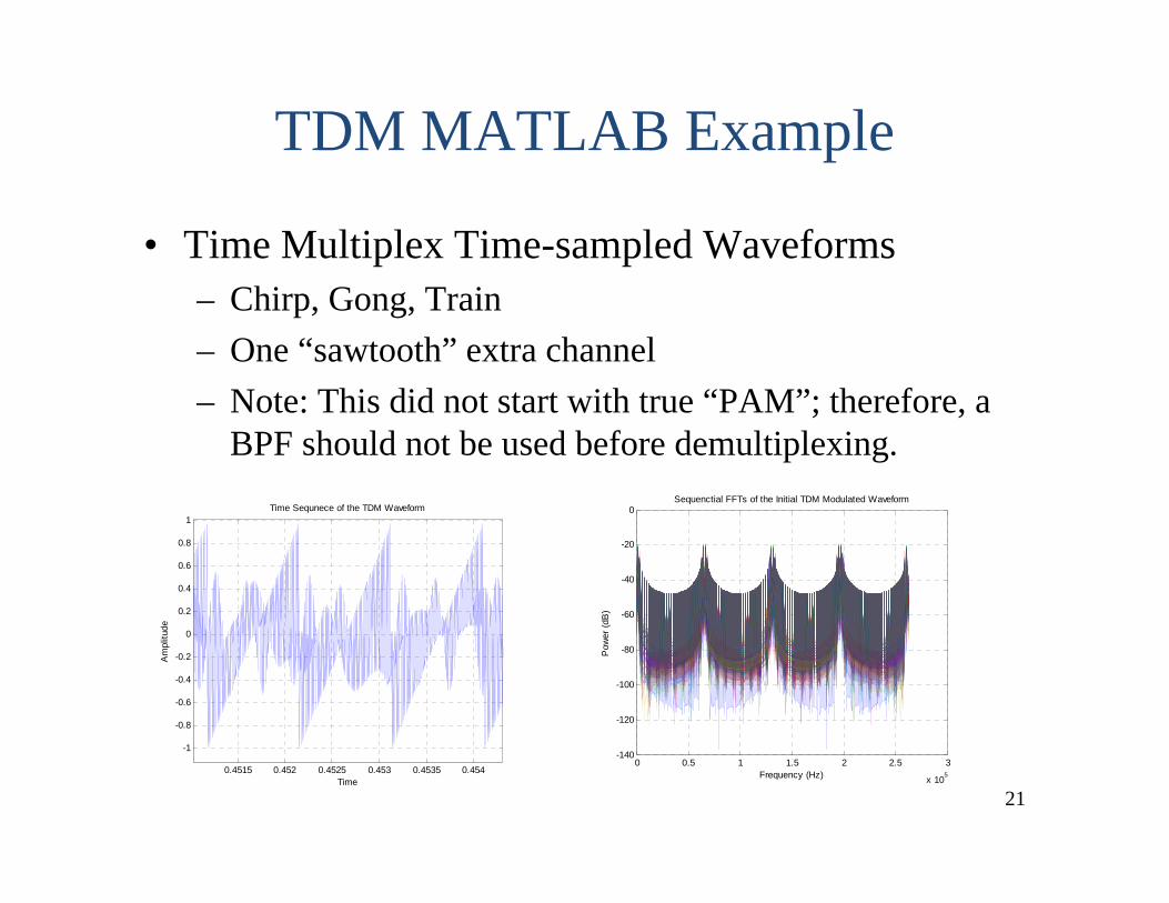
TDM MATLAB Example
• Time Multiplex Time-sampled Waveforms– Chirp, Gong, Train– One “sawtooth” extra channel– Note: This did not start with true “PAM”; therefore, a
BPF should not be used before demultiplexing.
21
0 0.5 1 1.5 2 2.5 3
x 105
-140
-120
-100
-80
-60
-40
-20
0Sequenctial FFTs of the Initial TDM Modulated Waveform
Frequency (Hz)
Pow
er (d
B)
0.4515 0.452 0.4525 0.453 0.4535 0.454
-1
-0.8
-0.6
-0.4
-0.2
0
0.2
0.4
0.6
0.8
1Time Sequnece of the TDM Waveform
Time
Am
plitu
de
22
Copyright © The McGraw-Hill Companies, Inc. Permission required for reproduction or display.
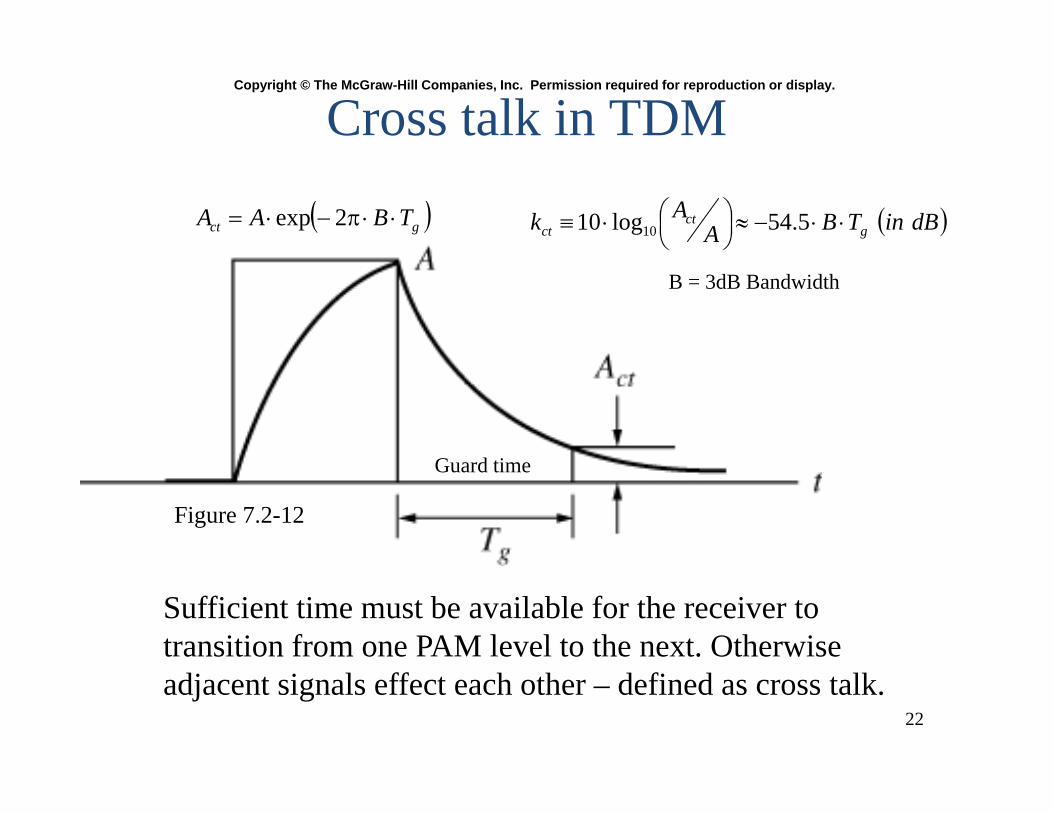
Cross talk in TDM
Sufficient time must be available for the receiver to transition from one PAM level to the next. Otherwise adjacent signals effect each other – defined as cross talk.
dBinTBAAk g
ctct
5.54log10 10
Guard time
B = 3dB Bandwidth
gct TBAA 2exp
Figure 7.2-12
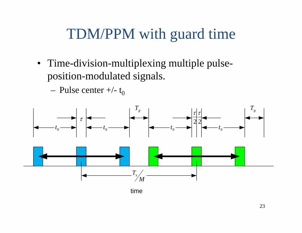
TDM/PPM with guard time
• Time-division-multiplexing multiple pulse-position-modulated signals.– Pulse center +/- t0
23
time
2
0t 0t
gT
MTs
0t2 gT
0t
2
2
0t 0t
gT
MTs
24
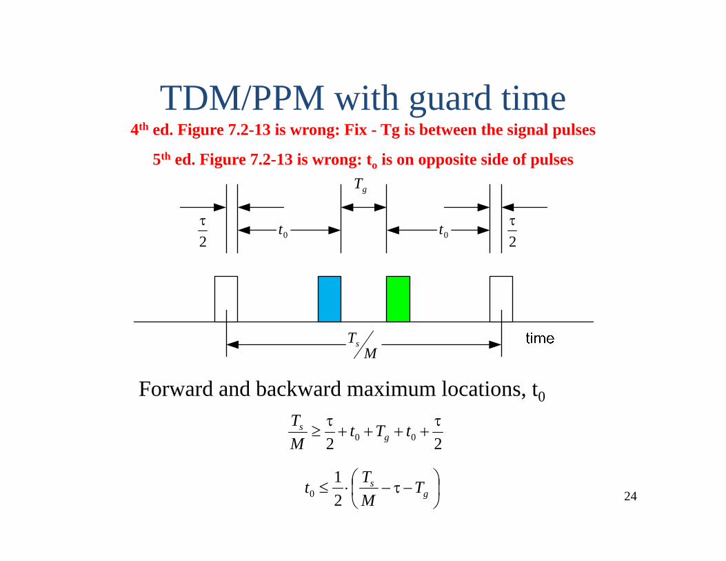
TDM/PPM with guard time
Forward and backward maximum locations, t0
22 00
tTtMT
gs
g
s TMTt
21
0
4th ed. Figure 7.2-13 is wrong: Fix - Tg is between the signal pulses
5th ed. Figure 7.2-13 is wrong: to is on opposite side of pulses
25
Comparing TDM and FDM
• TDM based on time slots– Overlap in frequency domain– Bandwidth of total signal defines cross talk– Well supported by digital circuitry, multiple mux rates– Synchronization concerns– Time based receiver; therefore, less dependent upon
filter performance or ripple
• FDM based on frequency slots– Overlap in time domain– Guard bands and filtering determine cross talk– Simple frequency assignments
26
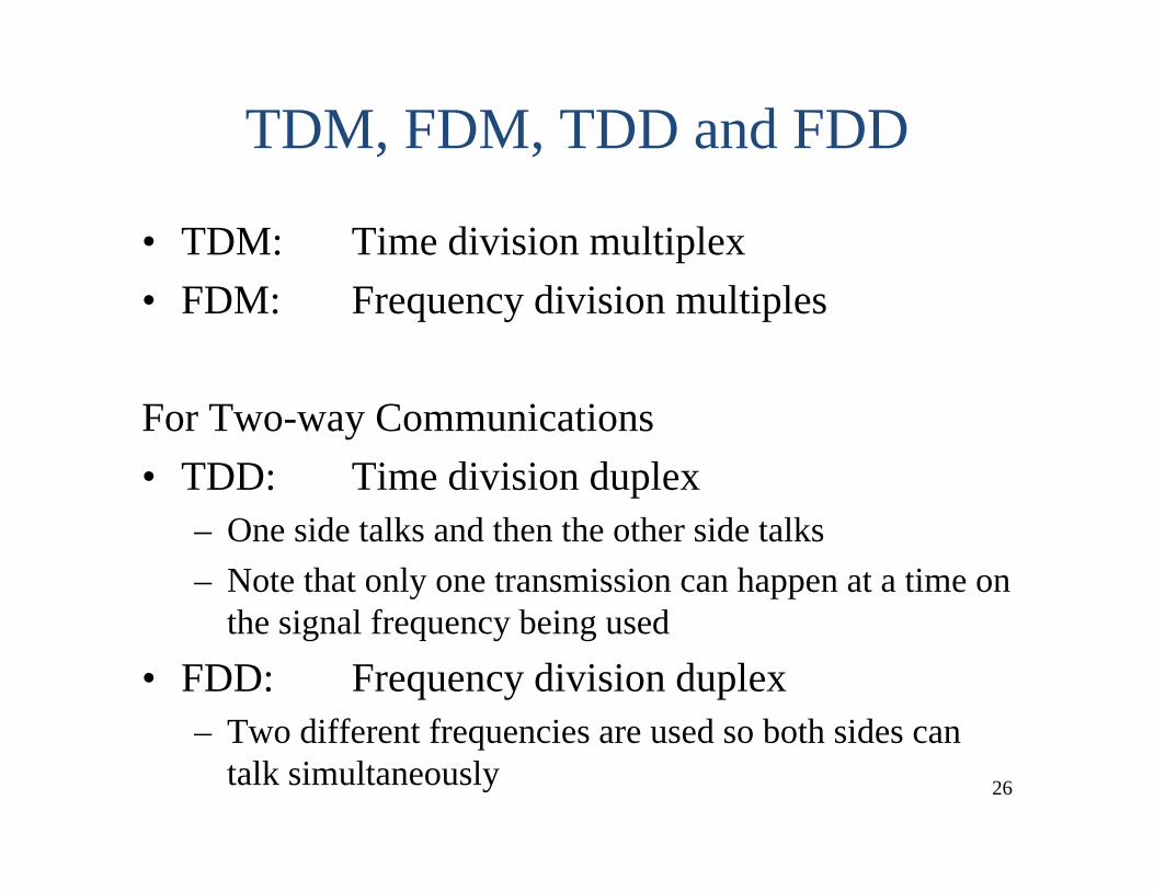
TDM, FDM, TDD and FDD
• TDM: Time division multiplex• FDM: Frequency division multiples
For Two-way Communications • TDD: Time division duplex
– One side talks and then the other side talks– Note that only one transmission can happen at a time on
the signal frequency being used
• FDD: Frequency division duplex– Two different frequencies are used so both sides can
talk simultaneously
27
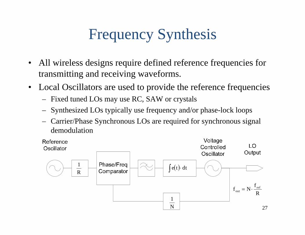
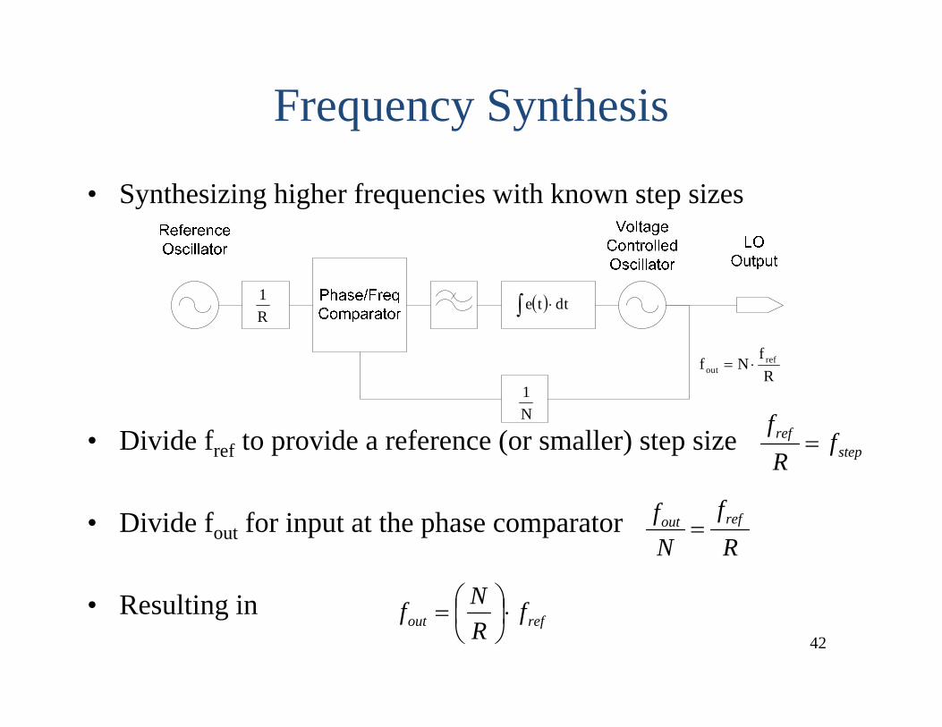
Frequency Synthesis
• All wireless designs require defined reference frequencies for transmitting and receiving waveforms.
• Local Oscillators are used to provide the reference frequencies– Fixed tuned LOs may use RC, SAW or crystals– Synthesized LOs typically use frequency and/or phase-lock loops– Carrier/Phase Synchronous LOs are required for synchronous signal
demodulation
R1 dtte
N1
Rf
Nf refout
28
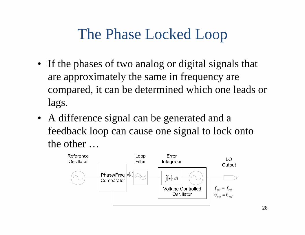
The Phase Locked Loop
• If the phases of two analog or digital signals that are approximately the same in frequency are compared, it can be determined which one leads or lags.
• A difference signal can be generated and a feedback loop can cause one signal to lock onto the other …
dtrefout ff
refout
te
29
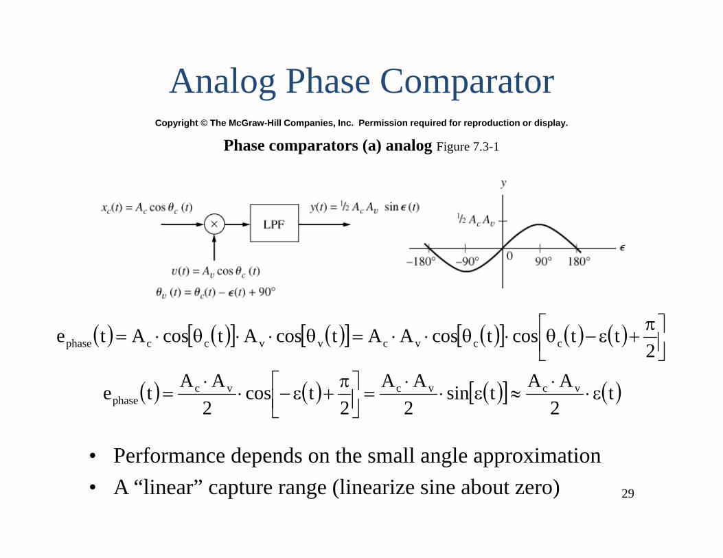
Copyright © The McGraw-Hill Companies, Inc. Permission required for reproduction or display.
Phase comparators (a) analog Figure 7.3-1
Analog Phase Comparator
• Performance depends on the small angle approximation • A “linear” capture range (linearize sine about zero)
2
ttcostcosAAtcosAtcosAte ccvcvvccphase
t2AAtsin
2AA
2tcos
2AAte vcvcvc
phase
30
Copyright © The McGraw-Hill Companies, Inc. Permission required for reproduction or display.
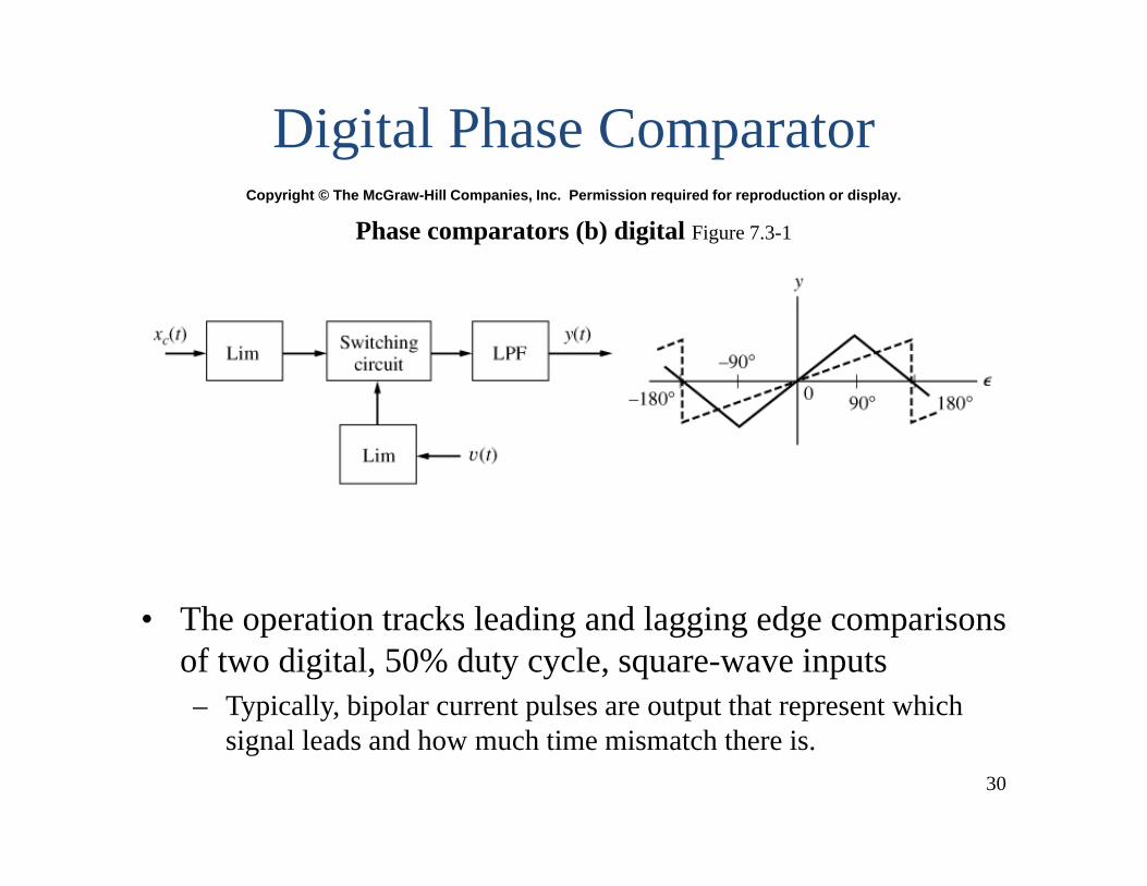
Phase comparators (b) digital Figure 7.3-1
Digital Phase Comparator
• The operation tracks leading and lagging edge comparisons of two digital, 50% duty cycle, square-wave inputs– Typically, bipolar current pulses are output that represent which
signal leads and how much time mismatch there is.
31
Copyright © The McGraw-Hill Companies, Inc. Permission required for reproduction or display.
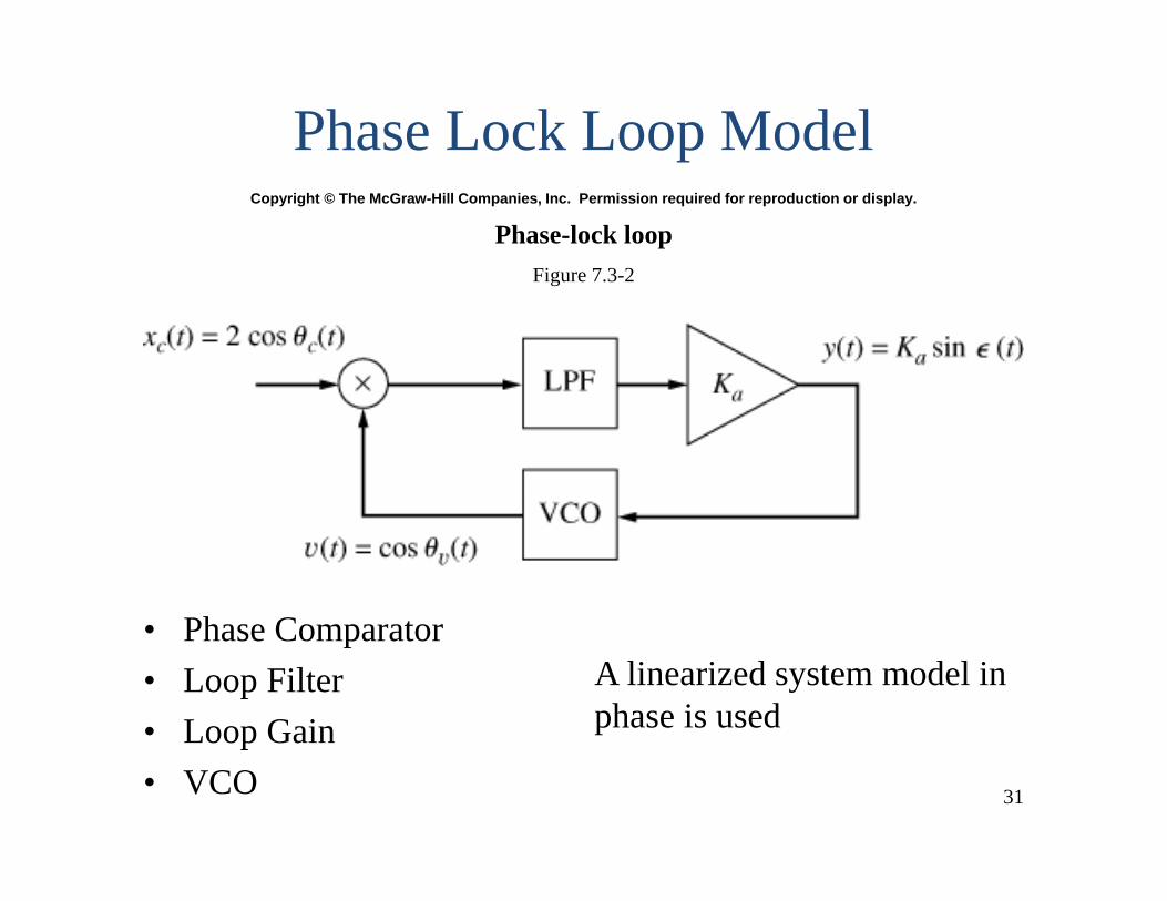
Phase-lock loopFigure 7.3-2
Phase Lock Loop Model
• Phase Comparator• Loop Filter• Loop Gain• VCO
A linearized system model in phase is used
32
Copyright © The McGraw-Hill Companies, Inc. Permission required for reproduction or display.
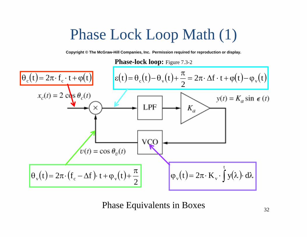
Phase-lock loop: Figure 7.3-2
Phase Lock Loop Math (1)
ttf2t cc
2
ttff2t vcv
t
vv dyK2t
tttf22
ttt vvc
Phase Equivalents in Boxes
33
Copyright © The McGraw-Hill Companies, Inc. Permission required for reproduction or display.
Phase-lock loop Figure 7.3-2
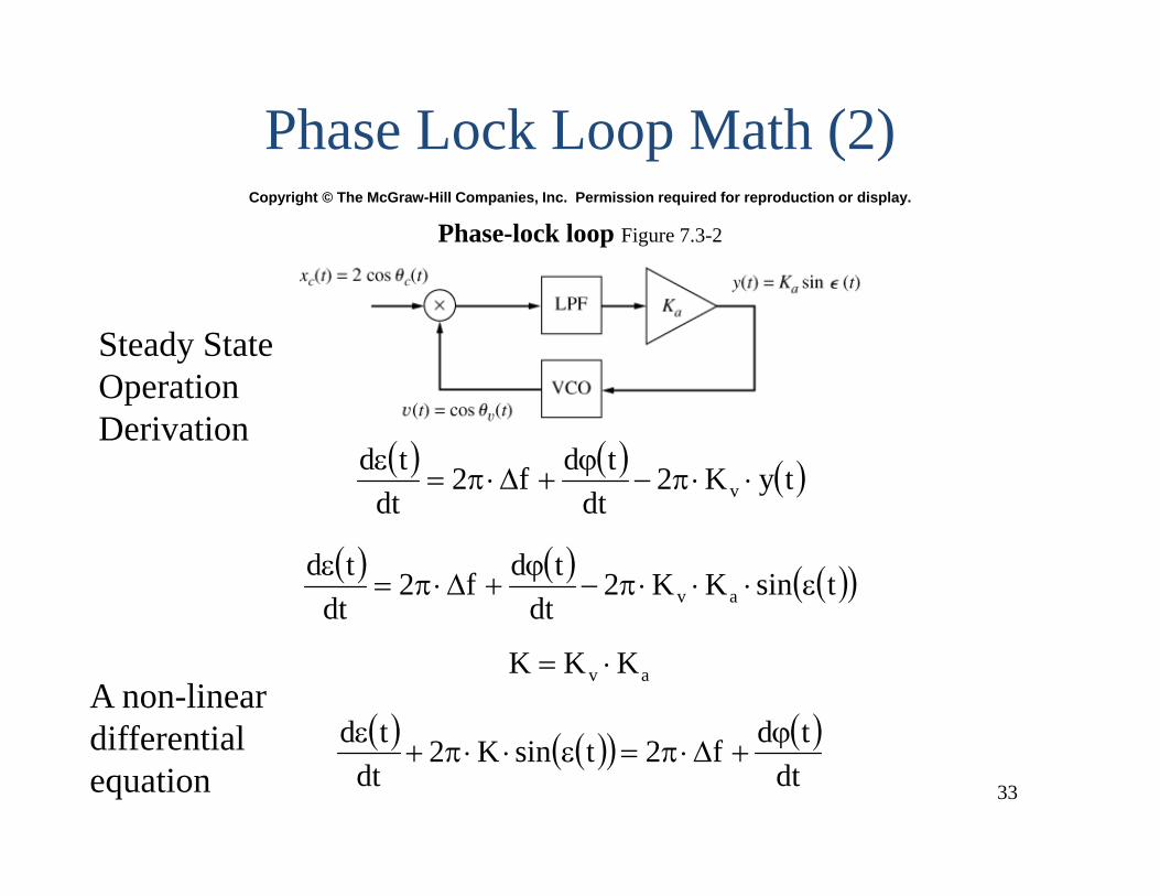
Phase Lock Loop Math (2)
tyK2dt
tdf2dt
tdv
dt
tdf2tsinK2dt
td
av KKK
tsinKK2dt
tdf2dt
tdav
Steady State Operation Derivation
A non-linear differential equation
34
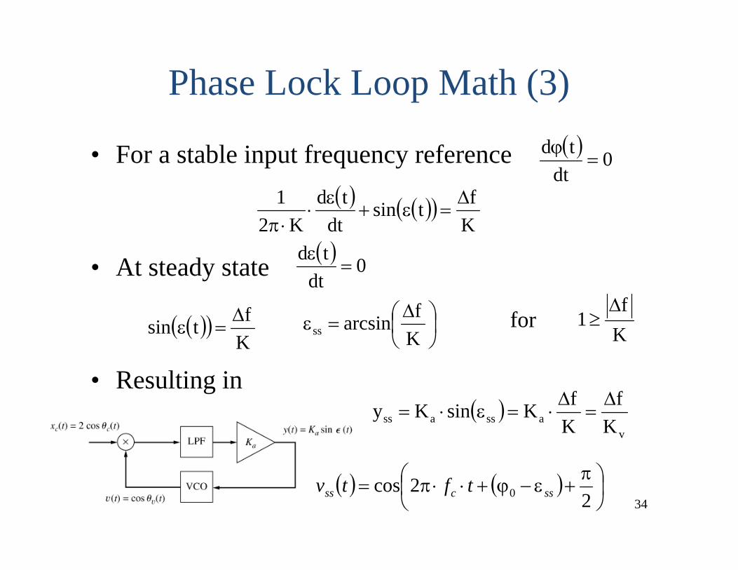
Phase Lock Loop Math (3)
• For a stable input frequency reference
• At steady state
• Resulting in
Kftsin
dttd
K21
Kftsin
Kfarcsinss K
f1
0dt
td
0dt
td
for
2
2cos 0 sscss tftv
v
assass Kf
KfKsinKy
35
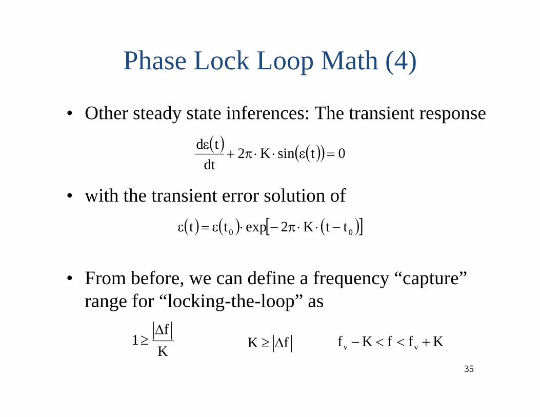
Phase Lock Loop Math (4)
• Other steady state inferences: The transient response
• with the transient error solution of
• From before, we can define a frequency “capture” range for “locking-the-loop” as
0tsinK2dt
td
00 ttK2exptt
Kf
1
fK KffKf vv
36
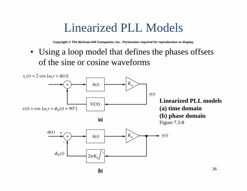
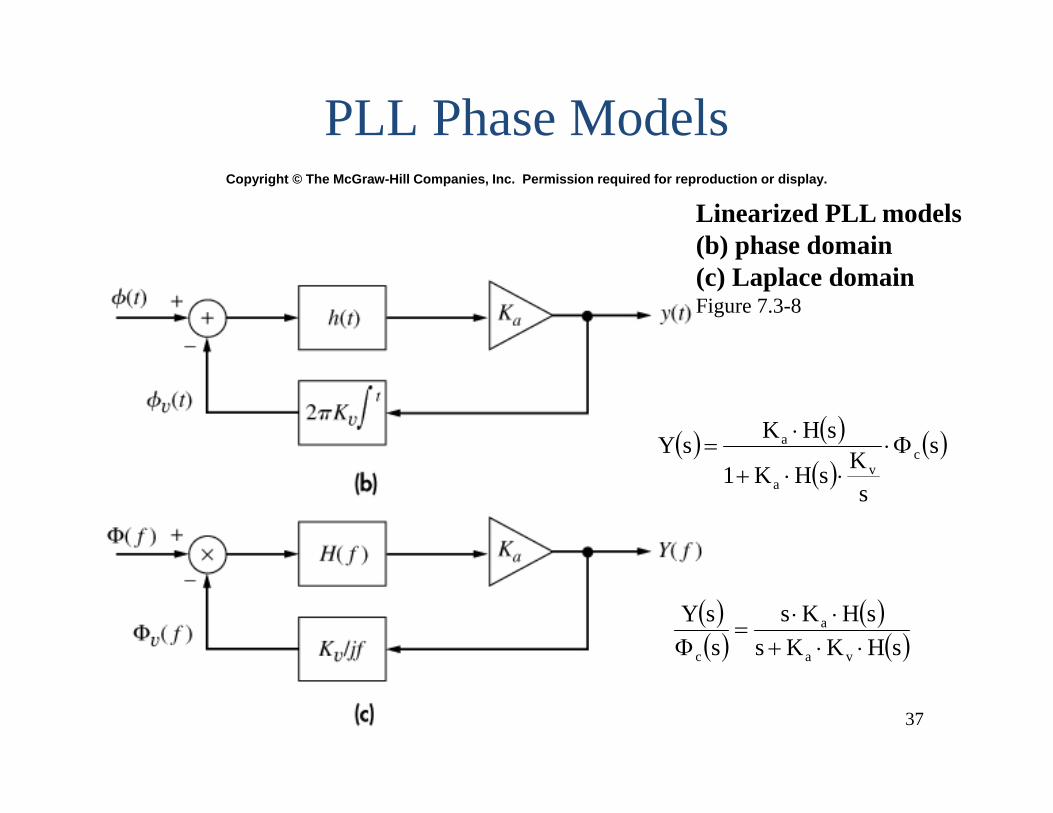
Linearized PLL Models
• Using a loop model that defines the phases offsets of the sine or cosine waveforms
Copyright © The McGraw-Hill Companies, Inc. Permission required for reproduction or display.
Linearized PLL models (a) time domain (b) phase domainFigure 7.3-8
37
Copyright © The McGraw-Hill Companies, Inc. Permission required for reproduction or display.
PLL Phase Models
s
sKsHK1
sHKsY cv
a
a
sHKKs
sHKsssY
va
a
c
Linearized PLL models (b) phase domain(c) Laplace domainFigure 7.3-8
38
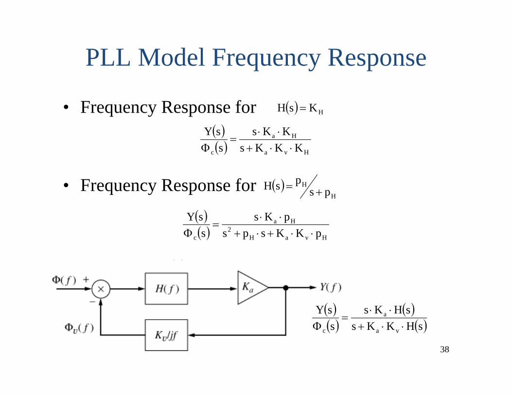
PLL Model Frequency Response
• Frequency Response for
• Frequency Response for
Hva
Ha
c KKKsKKs
ssY
HKsH
H
Hps
psH
HvaH
2Ha
c pKKspspKs
ssY
sHKKs
sHKsssY
va
a
c
39
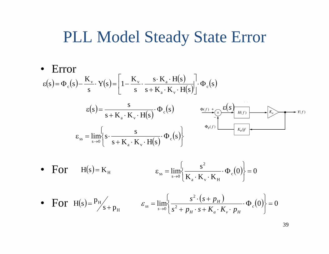
PLL Model Steady State Error
• Error
• For
• For 00lim 2
2
0
cHvaH
H
sss pKKspspss
ssHKKs
sHKss
K1sYs
Kss cva
avvc
ssHKKs
ss cva
HKsH 00KKK
slim cHva
2
0sss
ssHKKs
sslim cva
0sss
H
Hps
psH
s
40
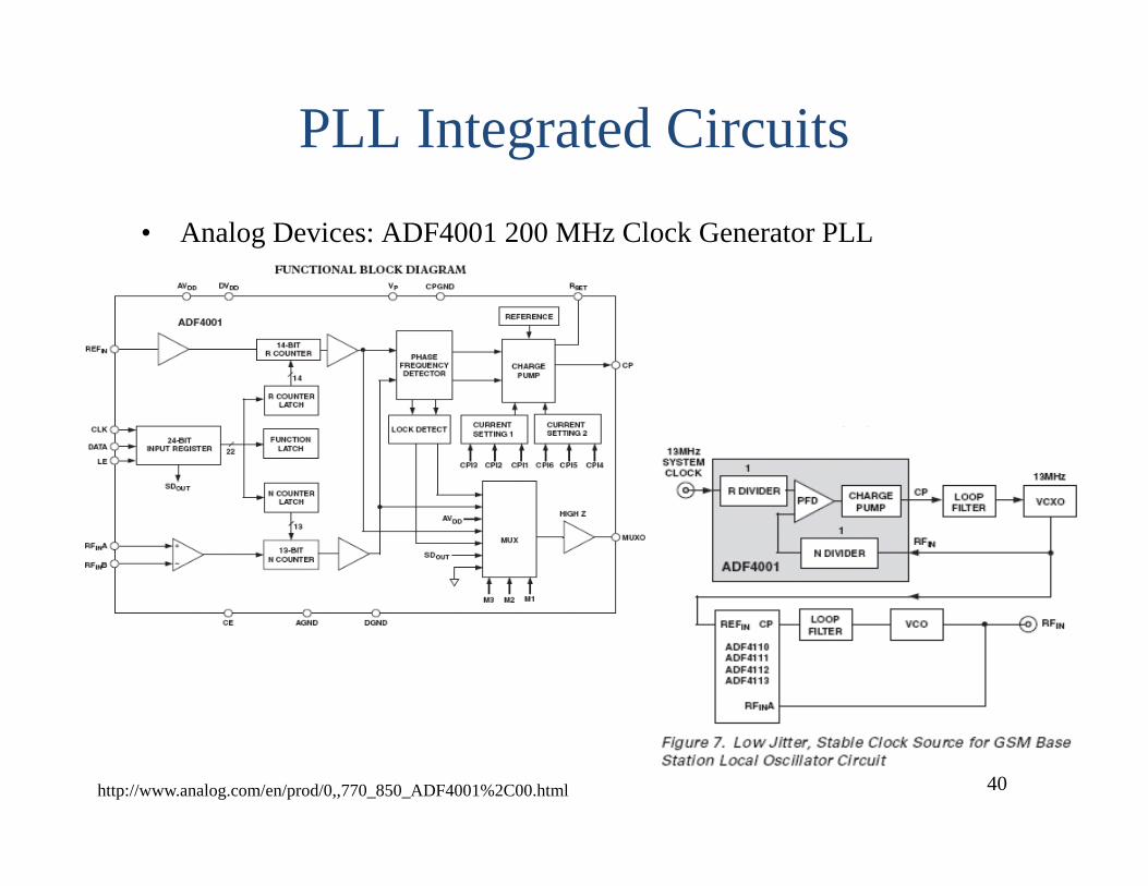
PLL Integrated Circuits• Analog Devices: ADF4001 200 MHz Clock Generator PLL
http://www.analog.com/en/prod/0,,770_850_ADF4001%2C00.html
41
Applications of PLL
• Frequency Synthesis– With tuning steps for radios
• Synchronous Signal Regeneration– FM Pilot, TV color burst, etc.– Coherent AM and DSB demodulator/detector
• Clock generation for digital electronics• FM demodulator/detector
… and much more
42
Frequency Synthesis
• Synthesizing higher frequencies with known step sizes
• Divide fref to provide a reference (or smaller) step size
• Divide fout for input at the phase comparator
• Resulting in
R1 dtte
N1
Rf
Nf refout
Rf
Nf refout
stepref fRf
refout fRNf
43
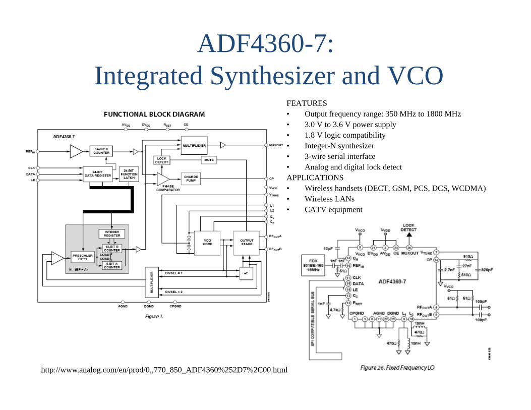
ADF4360-7:Integrated Synthesizer and VCO
FEATURES• Output frequency range: 350 MHz to 1800 MHz• 3.0 V to 3.6 V power supply• 1.8 V logic compatibility• Integer-N synthesizer• 3-wire serial interface• Analog and digital lock detectAPPLICATIONS• Wireless handsets (DECT, GSM, PCS, DCS, WCDMA)• Wireless LANs• CATV equipment
http://www.analog.com/en/prod/0,,770_850_ADF4360%252D7%2C00.html
44
PLL References
• Analog Devices Technical Articles• http://www.analog.com/library/analogDialogue/cd/vol33n1.pdf
– Phase Locked Loops for High-Frequency Receivers and Transmitters – Part 1
• http://www.analog.com/library/analogDialogue/cd/vol33n1.pdf#page=11
– Phase-Locked Loops for High-Frequency Receivers and Transmitters - Part 2
• http://www.analog.com/library/analogDialogue/cd/vol33n1.pdf#page=15
– Phase Locked Loops for High-Frequency Receivers and Transmitters – Part 3
• http://www.analog.com/library/analogDialogue/cd/vol33n1.pdf#page=20
Synchronous DetectionFrequency Synthesis
• The PLL provides a way to “adapt” to the incoming frequency and lock to the phase
• This is required for a “synchronous receiver” for any of the modulation forms previously described!
45
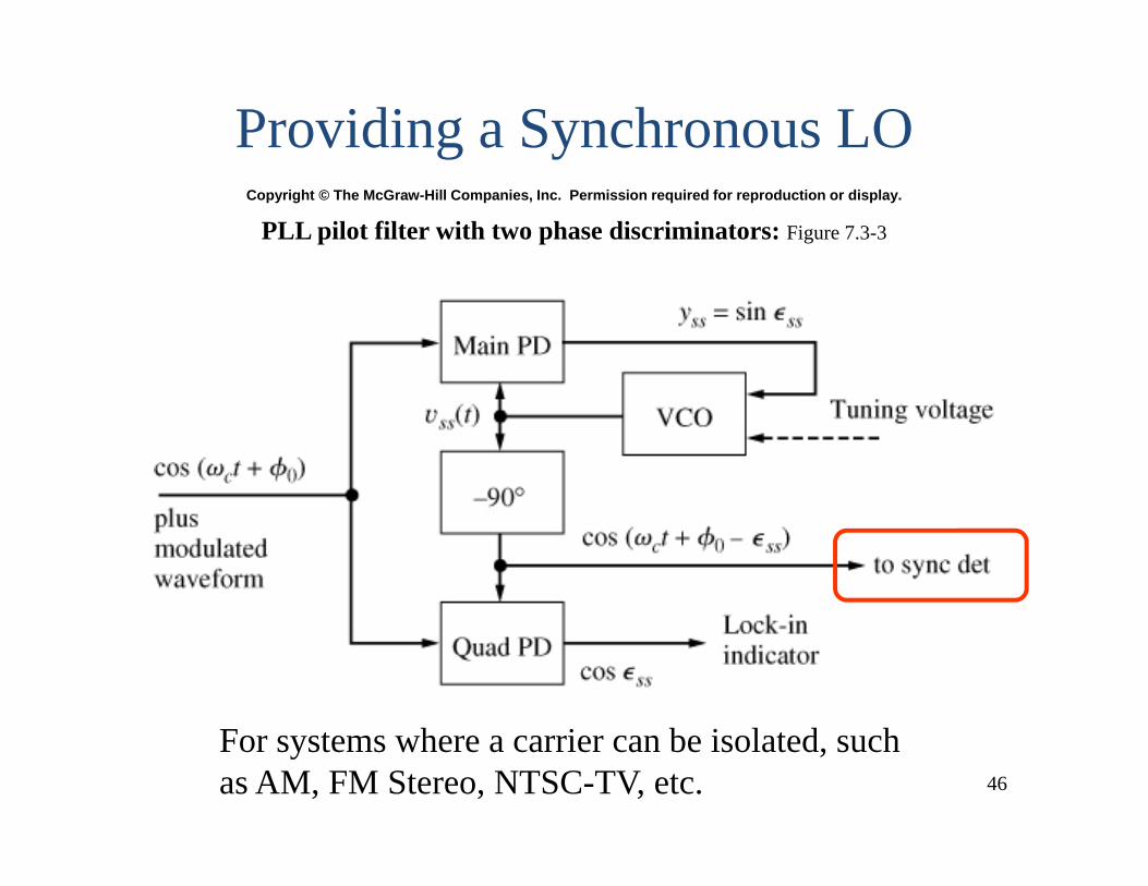
46
Copyright © The McGraw-Hill Companies, Inc. Permission required for reproduction or display.
PLL pilot filter with two phase discriminators: Figure 7.3-3
Providing a Synchronous LO
For systems where a carrier can be isolated, such as AM, FM Stereo, NTSC-TV, etc.
47
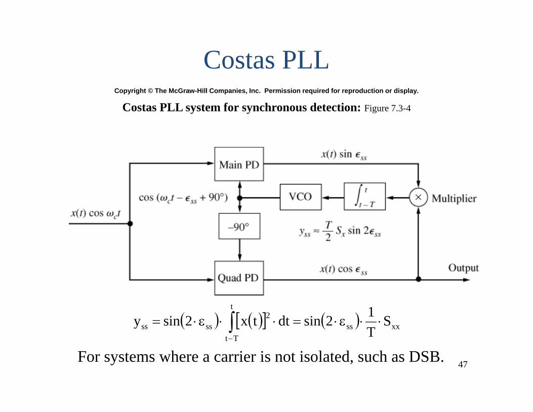
Copyright © The McGraw-Hill Companies, Inc. Permission required for reproduction or display.
Costas PLL system for synchronous detection: Figure 7.3-4
For systems where a carrier is not isolated, such as DSB.
Costas PLL
xxss
t
Tt
2ssss S
T12sindttx2siny
48
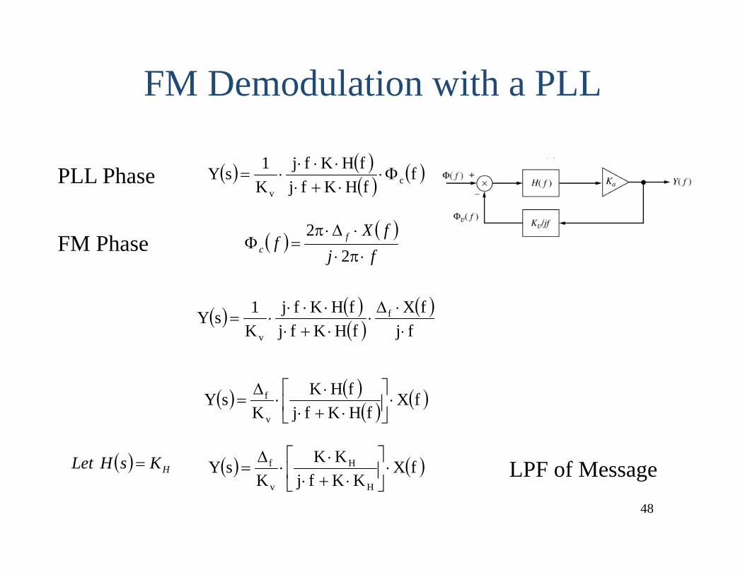
FM Demodulation with a PLL
ffHKfjfHKfj
K1sY c
v
fj
fXf f
c
22
fj
fXfHKfjfHKfj
K1sY f
v
fXfHKfj
fHKK
sYv
f
HKsHLet fXKKfj
KKK
sYH
H
v
f
FM Phase
LPF of Message
PLL Phase