Embed Size (px)
Citation preview
Comparison of Ultra-Thin InAs and InGaAs Quantum Wells and
Ultra-Thin-Body Surface-Channel MOSFETs
Cheng-Ying Huang1, Sanghoon Lee1, Evan Wilson3, Pengyu Long3, Michael Povolotskyi3, Varistha Chobpattana2, Susanne Stemmer2,
Arthur Gossard1,2, Gerhard Klimeck3, and Mark Rodwell1
1ECE, University of California, Santa Barbara 2Materials Department, University of California, Santa Barbara
3Network for Computational Nanotechnology, Purdue University, West Lafayette, IN
CSW/IPRM 2015
Santa Barbara, CA

Why III-V FETs? Why Ultra-thin channel?
• III-V channel: low electron effective mass high velocity, high mobility higher current at lower VDD reducing switching power
• Channel thickness (Tch) must be scaled in proportional to gate length (Lg) to maintain electrostatic integrity.
• For ultra-thin body (UTB) MOSFETs Tch~1/4 Lg, and for FinFETs Tch~1/2 Lg.
• At 7 or 5 nm nodes, channel thickness should be around 2-4 nm.
• Goal: Carefully examine InGaAs and InAs channels. The best design??
WFIN~8nm
Intel 14nm FinFET
Makr Bohr, IDF2014
tSi~5nm
STM-Leti-IBM
14nm UTBSOI IEDM2014
300K Si InAs InGaAs
me* 0.19 0.023 0.041
μe(cm2/V·s) 1450 33000 12000
μh(cm2/V·s) 370 450 <300
Eg(eV) 1.12 0.354 0.75
εr 11.7 15.2 13.9
a(Å) 5.43 6.0583 (InP)
Quantum confinement effects!! 2

Ultra-thin channel 2DEG: Hall results
0 1 2 3 4 5 6 7 80
2000
4000
6000
8000
10000
Mo
bil
ity
(c
m2/V
s)
Well Thickness (nm)
InAs channel
InGaAs channel
0 1 2 3 4 5 6 7 81.2
1.4
1.6
1.8
2.0
2.2
Ca
rrie
r c
on
ce
ntr
ati
on
(10
12c
m-2
)
Well Thickness (nm)
InAs channel
InGaAs channel
• Quantum well (QW) 2DEGs were grown by solid source MBE.
• For wide wells: μInAs > μInGaAs
• For narrow wells (~2 nm): μInAs ≈ μInGaAs
• Carrier concentration decreases due to increased E0.
3

What happens in thin wells?
0 5 10 15 200.02
0.03
0.04
0.05
0.06
0.07
0.08
0.09
0.10
InAs
In-p
lan
e e
ffe
cti
ve
ma
ss
, m
// (m
0)
Well Thickness (nm)
InGaAs/InP, Nag1993
InAs/InP, Nag1993
InGaAs/InP, Wetzel1992
InGaAs/InP, Hrivnak1992
InAs, Mugny2015
Schneider1995
Wiesner1994
Wetzel1996
InGaAs
• Mobility is limited by interface roughness scattering. Strained InAs growth (S-K mode) might induce higher interface roughness.
• Electron effective mass are similar for ~2-3 nm InAs and InGaAs wells because of non-parabolic band effects.
5 10 15 2010
2
103
104
105
106
107
Mo
bil
ity
(c
m2V
-1s
-1)
Well thickness(nm)
300K
total
interface roughness
remote impurity
InGaAs
well
polar optical phononalloy
acoustic phonon
C. Y. Huang et al., J. Appl. Phys. 115, 123711 (2013)
µ ~Tch-6
4
J. Appl. Phys. 77, 2828 (1995), Phys. Rev. B, 52, 1038 (1996),
Appl. Phys. Lett 64, 2520 (1994), Appl. Phys. Lett 62, 2416 (1993),
G. Mugny et al., EUROSOI-ULSI conference 2015.

Ultra-thin body III-V FETs: Lg~40 nm
5
-0.2 0.0 0.2 0.4 0.610
-9
10-8
10-7
10-6
10-5
10-4
10-3
10-2
10-1
100
101
I D (
mA
/m
)
VGS
(V)
VDS
= 0.1 to 0.7 V
0.2 V increment
-0.2 0.0 0.2 0.4 0.6
g
m (m
S/
m)
VGS
(V)
0.0
0.4
0.8
1.2
1.6
2.0
2.4V
DS = 0.1 to 0.7 V
0.2 V increment
0.0 0.2 0.4 0.60.0
0.5
1.0
1.5
I D (
mA
/m
)
VDS
(V)
Ron
= 292 Ohm-m
at VGS
= 1.0 V
VGS
= -0.2 V to 1.0 V
0.2 V increment
0.2 0.4 0.6
VDS
(V)
Ron
= 400 Ohm-m
at VGS
= 1.0 V
VGS
= -0.2 V to 1.0 V
0.2 V increment
• UTB FETs with 3 nm channels were fabricated to compare InAs and InGaAs channels.
• 1.6:1 Ion and transcoaductance for InAs channels.
• 10:1 lower Ioff for InGaAs channels.
InAs InGaAs
InGaAs InAs

On-state performance
0.1 10.0
0.4
0.8
1.2
1.6
2.0
2.4
VDS
= 0.5 V
Gate length (m)
3 nm InAs
3 nm InGaAs
Pe
ak
gm
(m
S/
m)
100 10000
100
200
300
400
5003 nm InAs
3 nm InGaAs
Io
n (A
/m
)
Gate length (nm)
VDS
= 0.5 V
Ioff
= 100 nA/m
0.0 0.1 0.20
250
500
750
1000
RS/D
~ 19020 Ohmm
VGS
= 1 V
Ro
n(O
hm
m
)
Gate length (m)
3 nm InAs
3 nm InGaAs
• Higher Ion and higher gm for UTB InAs FETs than InGaAs UTB FETs.
• InAs FETs achieve gm=2 mS/μm, and Ion=400 μA/μm at VDS=0.5V and Ioff=100 nA/μm.
• Similar source/drain resistance (RS/D ) ensures that the performance degradation of InGaAs is not from source/drain, but from channel itself (slope).
6

Subthreshold swing and off-state current
0.1 160
80
100
120
Gate Length (m)
Su
bth
res
ho
ld S
win
g (
mV
/de
c)
VDS
=0.1 V,3 nm InAs
VDS
=0.5 V,3 nm InAs
VDS
=0.1 V,3 nm InGaAs
VDS
=0.5 V,3 nm InGaAs
0.1 10
50
100
150
Vth at 1 A/m
DIB
L (
mV
/V)
Gate length (m)
3 nm InAs
3 nm InGaAs
100 100010
-3
10-2
10-1
100
101
102
3 nm InAs
3 nm InGaAs
IO
FF
, M
IN (
nA
/m
)
Gate length (nm)
VDS
= 0.5 V
• Superior SS~83 mV/dec. and DIBL~110 mV/V because of ultra-thin channels and improved electrostatics.
• Minimum Ioff is 10:1 lower for InGaAs channel at short Lg, where leakage current limited by band-to-band tunneling.
• InGaAs FETs are limited by gate leakage at long Lg.
7

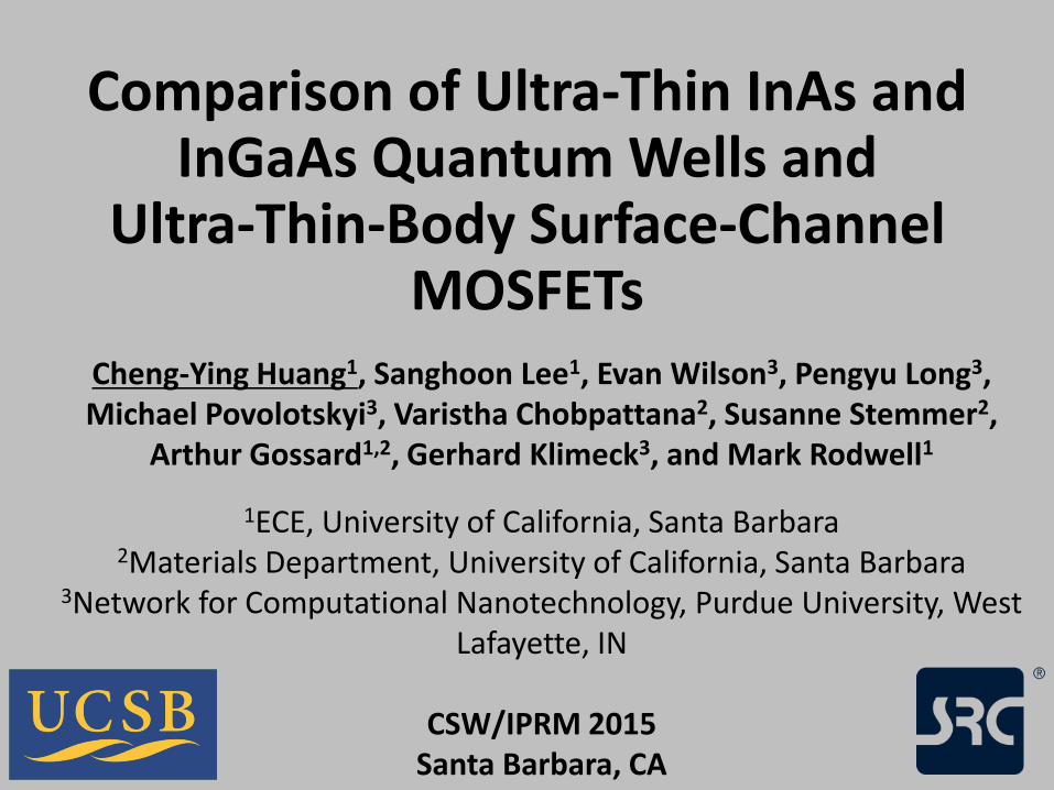
Why QW-2DEGs and UTB-FETs show different results?
• 1st possible cause: Electron population in L valley due to strong quantum confinement Unlikely.
2nm InAlAs barrier,
3nm InGaAs channel
with H passivation
on top
Courtesy of Evan Wilson, Pengyu Long, Michael Povolotskyi, and Gerhard Klimeck.
2nm InAlAs barrier,
3nm InAs channel
with H passivation
on top
In0.53Ga0.47As InAs
me* at Γ [m0] 0.080 0.063
Γ – L separation [eV] 0.596 0.905
Eg at Γ [eV] 1.06 0.639 8
Why QW-2DEGs and UTB-FETs show different results?
• 2nd possible cause: Electron interaction with oxide traps inside conduction band Likely.
• Electrons in high In% content channels have less scattering and less electron capture by the oxide traps.
9
J. Robertson et al., J. Appl. Phys. 117, 112806 (2015)
J. Robertson, Appl. Phys. Lett. 94, 152104 (2009)
N. Taoka et al., Trans. Electron Devices. 13, 456 (2011)
N. Taoka et al., IEEE IEDM 2011, 610.

UCSB Lg~12 nm III-V MOSFETs (DRC 2015)
N+InGaAs
InP spacer
InAlAs
Barrier
Lg~12nm
~ 8nm
10
tch~ 2.5 nm (1.5/1 nm InGaAs/InAs)
Ni N+InP
Ion/Ioff>8.3·105
-0.2 0.0 0.2 0.4 0.6 0.810
-8
10-7
10-6
10-5
10-4
10-3
10-2
10-1
100
101
gm (m
S/
m)I D
(m
A/
m)
VGS
(V)
0.0
0.4
0.8
1.2
1.6
2.0
2.4
SS~107 mV/dec.
SS~98 mV/dec.
VDS
= 0.1 to 0.7 V, 0.2 V increment
0.0 0.1 0.2 0.3 0.4 0.5 0.6 0.70.0
0.5
1.0
1.5
I D (
mA
/m
)V
DS (V)
Ron
= 302 Ohm-m
at VGS
= 1.0 V
VGS
= -0.2 V to 1.2 V
0.2 V increment

Summary
11
• Below 10 nm logic nodes, ultrathin channels are required.
• In QW 2DEGs, the electron Hall mobility are similar for InGaAs and InAs wells as the wells thinned to 2~3nm.
• In UTB MOSFETs, 3 nm InAs channels significantly improve on-state current and transconductance (~1.6:1), and reduce channel resistance as compared to 3 nm InGaAs channel.
• Purdue’s tight-binding calculations show large ~0.6 eV Γ–L splitting in 3 nm InGaAs channels, ruling out the possibility of electron population in L-valley.
• UCSB C-V measurements show large dispersion in 3 nm InGaAs channels, possibly indicating the significant electron interactions with oxide traps. (As-As anti-bonding may be the culprit)

Thanks for your attention!
Questions?
• This research was supported by the SRC Non-classical CMOS
Research Center (Task 1437.009) and GLOBALFOUNDRIES(Task
2540.001).
• A portion of this work was done in the UCSB nanofabrication
facility, part of NSF funded NNIN network.
• This work was partially supported by the MRSEC Program of the
National Science Foundation under Award No. DMR 1121053.
Acknowledgment
(backup slides follow)

Mobility in different channel design: 25 µm-Lg
0 1 2 3 4 5 6 70
200
400
600
800
1000
1200
Mo
bil
ity
(c
m2/V
s)
Carrier density (cm-2)
4.5 nm InGaAs
2.5 nm InAs
5.0 nm InAs
-0.2 0.0 0.2 0.4 0.6 0.80.0
0.5
1.0
1.5
2.0
2.5
3.0
Ca
rrier d
en
sity
(1
01
2 cm
-2)
Eff
ec
tiv
e C
G (F
/cm
2)
VGS
(V)
0
2
4
6
8
Freq.: 200 kHz
W/L=25m/21m
4.5 nm InGaAs
2.5 nm InAs
5.0 nm InAs
m*, Cg-ch, RS/D more important for ballistic FETs