Embed Size (px)
DESCRIPTION
COMPUTER ARCHITECTURE. Processor: Single-Cycle Datapath. (Based on text: David A. Patterson & John L. Hennessy, Computer Organization and Design: The Hardware/Software Interface , 3 rd Ed., Morgan Kaufmann, 2007 ). COURSE CONTENTS. Introduction Instructions Computer Arithmetic - PowerPoint PPT Presentation
Citation preview
1
(Based on text: David A. Patterson & John L. Hennessy, Computer Organization and Design: The Hardware/Software Interface, 3rd Ed., Morgan Kaufmann, 2007)
Processor:Processor:Single-Cycle DatapathSingle-Cycle Datapath
2
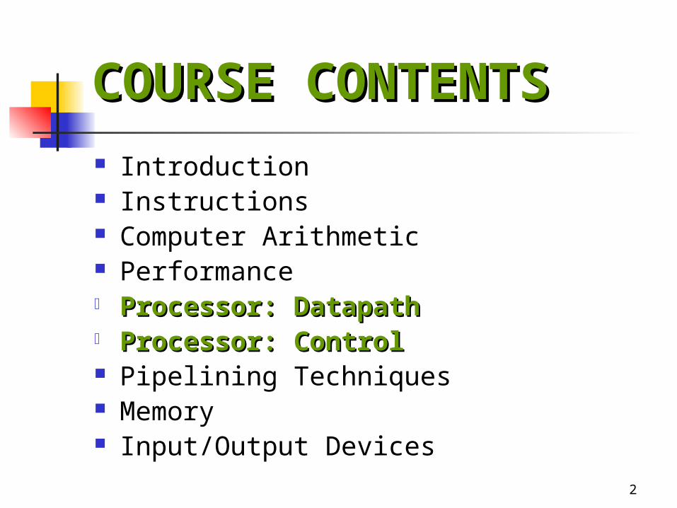
COURSE CONTENTSCOURSE CONTENTS Introduction Instructions Computer Arithmetic Performance Processor: DatapathProcessor: Datapath Processor: ControlProcessor: Control Pipelining Techniques Memory Input/Output Devices
3
PROCESSOR: PROCESSOR: DATAPATH & CONTROLDATAPATH & CONTROL
Elements of Datapath Single-Cycle Datapath
4
Subset of MIPS Subset of MIPS InstructionsInstructions
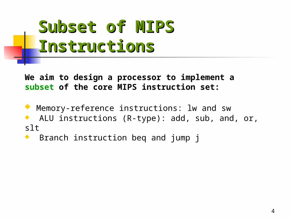
We aim to design a processor to implement a subset of the core MIPS instruction set:
Memory-reference instructions: lw and sw ALU instructions (R-type): add, sub, and, or, slt Branch instruction beq and jump j
5
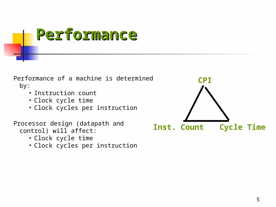
Performance of a machine is determined by:• Instruction count• Clock cycle time• Clock cycles per instruction
Processor design (datapath and control) will affect:
• Clock cycle time• Clock cycles per instruction
CPI
Inst. Count Cycle Time
PerformancePerformance
6
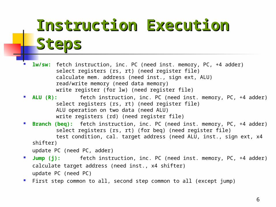
lw/sw: fetch instruction, inc. PC (need inst. memory, PC, +4 adder)select registers (rs, rt) (need register file)calculate mem. address (need inst., sign ext, ALU)read/write memory (need data memory)write register (for lw) (need register file)
ALU (R): fetch instruction, inc. PC (need inst. memory, PC, +4 adder) select registers (rs, rt) (need register file) ALU operation on two data (need ALU)write registers (rd) (need register file)
Branch (beq): fetch instruction, inc. PC (need inst. memory, PC, +4 adder) select registers (rs, rt) (for beq) (need register file)test condition, cal. target address (need ALU, inst., sign ext,
x4 shifter) update PC (need PC, adder) Jump (j): fetch instruction, inc. PC (need inst. memory, PC, +4 adder)
calculate target address (need inst., x4 shifter)update PC (need PC)
First step common to all, second step common to all (except jump)
Instruction Execution Instruction Execution StepsSteps
7
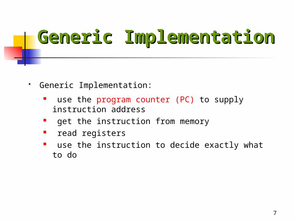
Generic Implementation:
use the program counter (PC) to supply instruction address
get the instruction from memory read registers use the instruction to decide exactly what to do
Generic Generic ImplementationImplementation
8
Resources NeededResources Needed
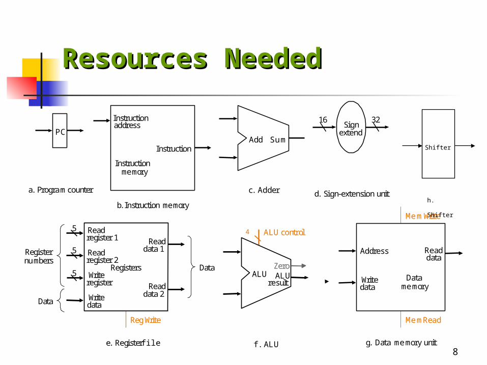
Instructionmemory
Instructionaddress
Instruction
b. Instruction memory
PC
a. Program counter
Add Sum
c. Adder
RegWrite
RegistersWriteregister
Readdata 1
Readdata 2
Readregister 1
Readregister 2
WritedataData
Data
Registernumbers
e. Register file
5
5
5 ALU control
ALUresult
ALU
f . ALU
Zero
4
16 32Sign
extend
d. Sign-extension unit
MemRead
MemWrite
Datamemory
Writedata
Readdata
g. Data memory unit
Address
Shifter
h. Shifter
9
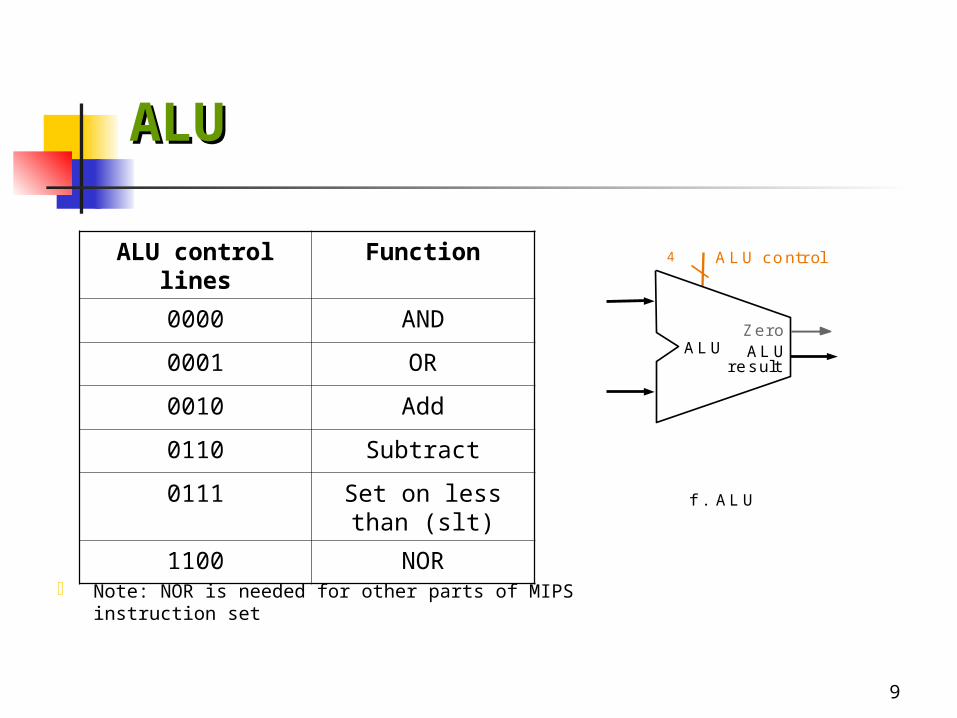
ALUALU
A L U co n tr o l
A L Ure s u lt
A L U
f . A L U
Z e ro
4ALU control lines
Function
0000 AND
0001 OR
0010 Add
0110 Subtract
0111 Set on less than (slt)
1100 NOR
Note: NOR is needed for other parts of MIPS instruction set
10
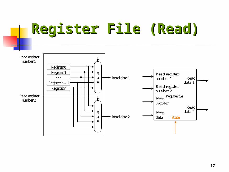
Register File (Read)Register File (Read)
Mux
Register 0Register 1
Register n – 1Register n
Mux
Read data 1
Read data 2
Read registernumber 1
Read registernumber 2
Read registernumber 1 Read
data 1
Readdata 2
Read registernumber 2
Register fileWriteregister
Writedata Write
11
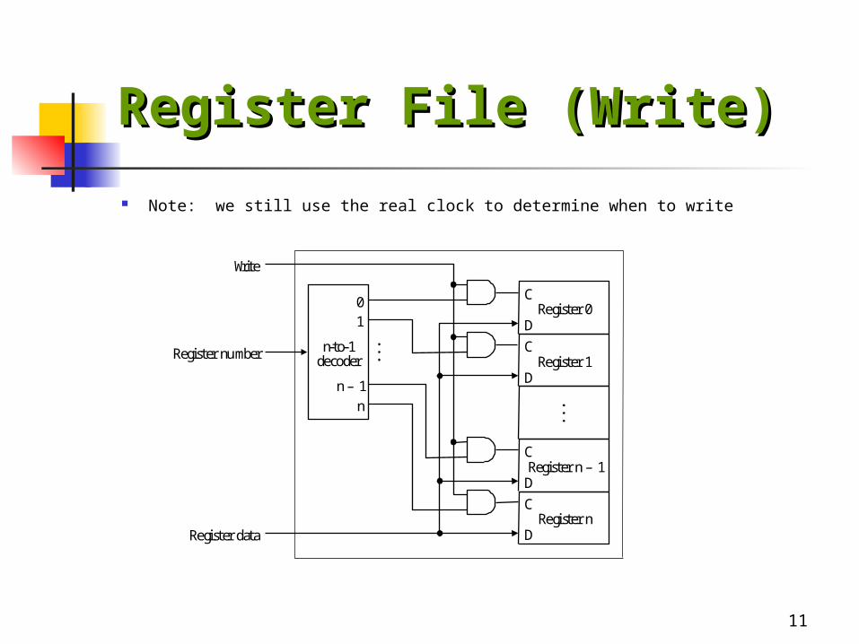
Register File (Write)Register File (Write)
Note: we still use the real clock to determine when to write
n-to-1decoder
Register 0
Register 1
Register n – 1C
C
D
DRegister n
C
C
D
D
Register number
Write
Register data
01
n – 1n
12
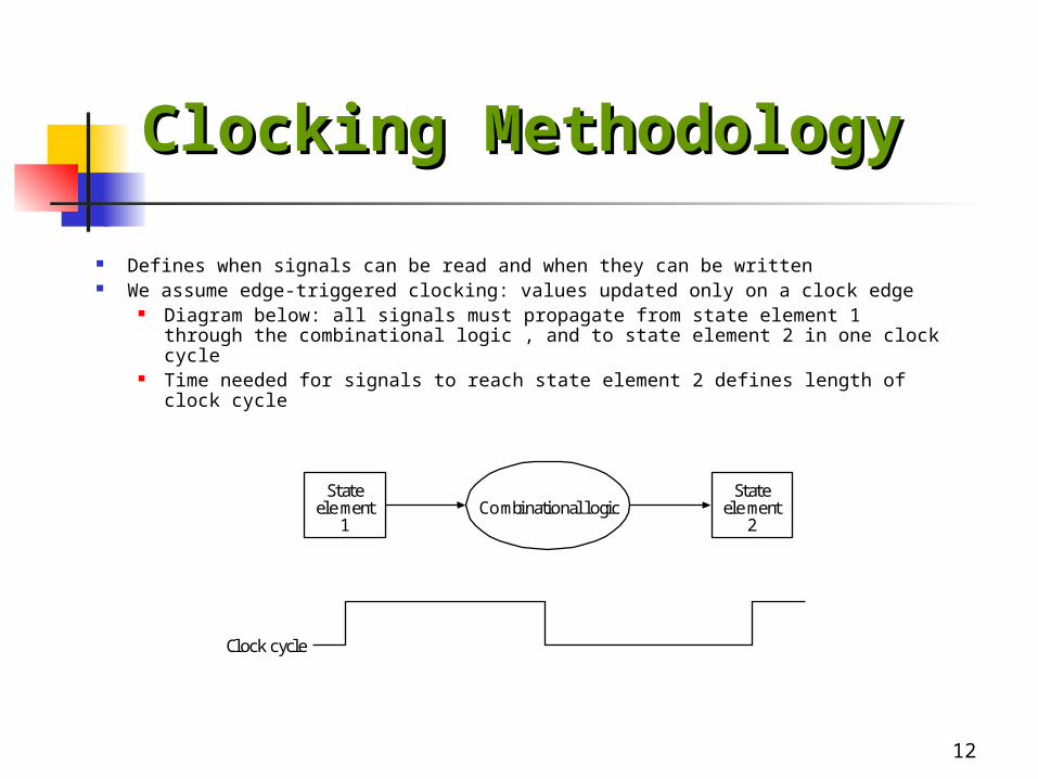
Defines when signals can be read and when they can be written We assume edge-triggered clocking: values updated only on a clock edge
Diagram below: all signals must propagate from state element 1 through the combinational logic , and to state element 2 in one clock cycle
Time needed for signals to reach state element 2 defines length of clock cycle
Clocking MethodologyClocking Methodology
Clock cycle
Stateelement
1Combinational logic
Stateelement
2
13
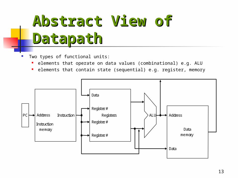
Two types of functional units: elements that operate on data values (combinational) e.g. ALU elements that contain state (sequential) e.g. register, memory
Abstract View of Abstract View of DatapathDatapath
Registers
Register #
Data
Register #
Datamemory
Address
Data
Register #
PC Instruction ALU
Instructionmemory
Address
14
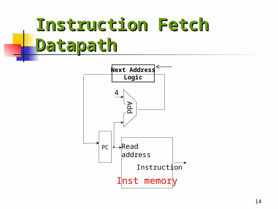
Instruction Fetch Instruction Fetch DatapathDatapath
Add
4
PC Readaddress
Instruction
Inst memory
Next AddressLogic
15
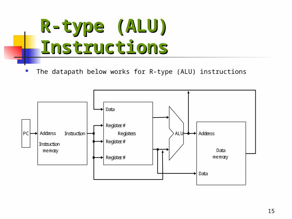
The datapath below works for R-type (ALU) instructions
R-type (ALU) R-type (ALU) InstructionsInstructions
Registers
Register #
Data
Register #
Datamemory
Address
Data
Register #
PC Instruction ALU
Instructionmemory
Address
16
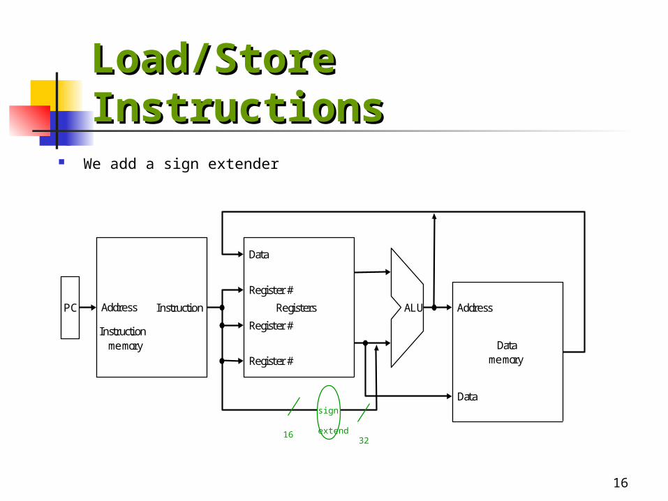
We add a sign extender
Load/Store InstructionsLoad/Store Instructions
Registers
Register #
Data
Register #
Datamemory
Address
Data
Register #
PC Instruction ALU
Instructionmemory
Address
sign
extend1632
17
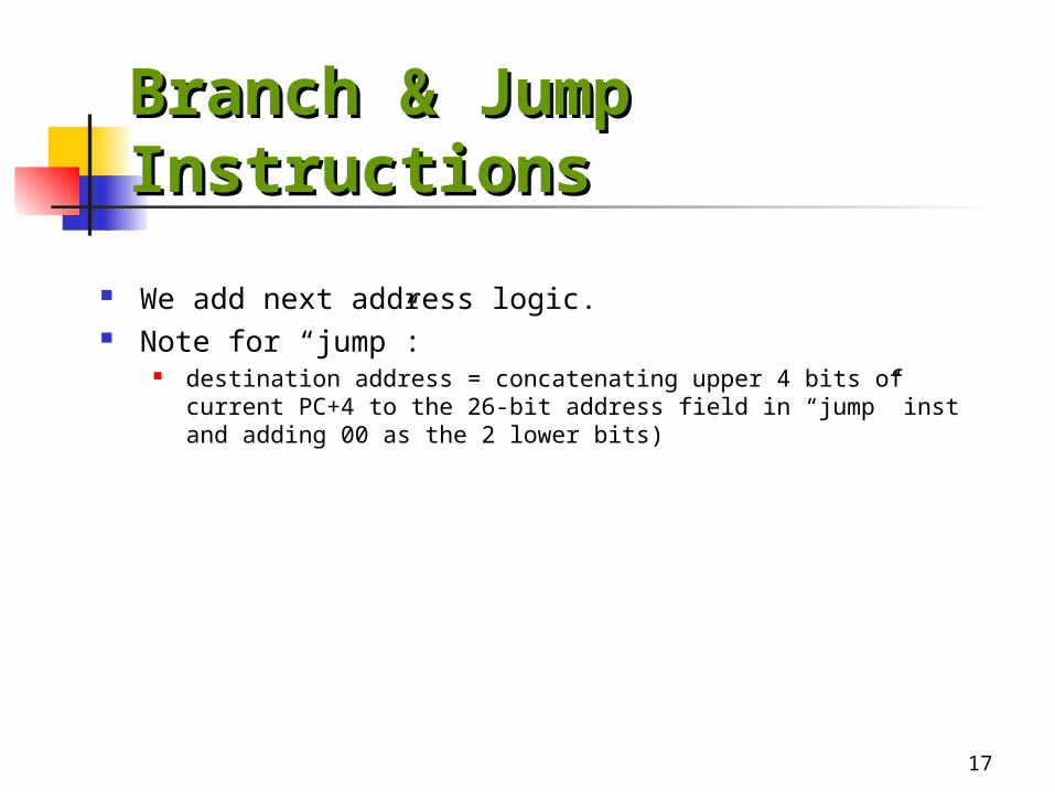
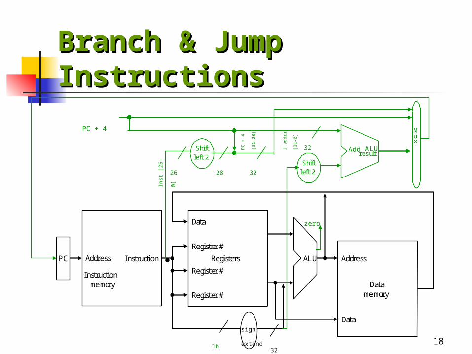
We add next address logic. Note for “jump”:
destination address = concatenating upper 4 bits of current PC+4 to the 26-bit address field in “jump” inst and adding 00 as the 2 lower bits)
Branch & Jump Branch & Jump InstructionsInstructions
18
Registers
Register #
Data
Register #
Datamemory
Address
Data
Register #
PC Instruction ALU
Instructionmemory
Address
sign
extend16 32
Add ALUresult
Mux
Shiftleft 2
PC + 4
zero
Inst
[2
5-0
]
Shiftleft 2
26 28
PC
+ 4
[31
-28
]
32
J ad
drr
[31
-0]
32
Branch & Jump Branch & Jump InstructionsInstructions
19
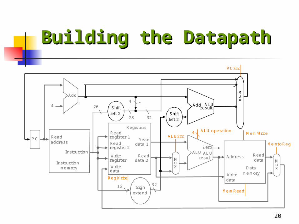
Building the DatapathBuilding the Datapath
Use multiplexers (MUX) to stitch them together Do not duplicate functional units common to
different instructions Add control signals (for MUX selection, ALU
operation, state element read/write) Independent operations can be in parallel
20
P C
Instructionmemory
Readaddress
Instruction
16 32
Registers
W riteregister
W ritedata
Readdata 1
Readdata 2
Readregister 1
Readregister 2
4
Mux
A LU o pe ration4
RegW rite
Mem Read
M em WriteALUSrc
M emtoReg
ALUresu lt
Z eroALU
Datamem ory
Add ress
Writeda ta
Readdata M
ux
Signextend
Add
Add A LUresult
Mux
PCSrc
Shiftlef t 2
Shift
left 2
264
28 32
Building the DatapathBuilding the Datapath
21
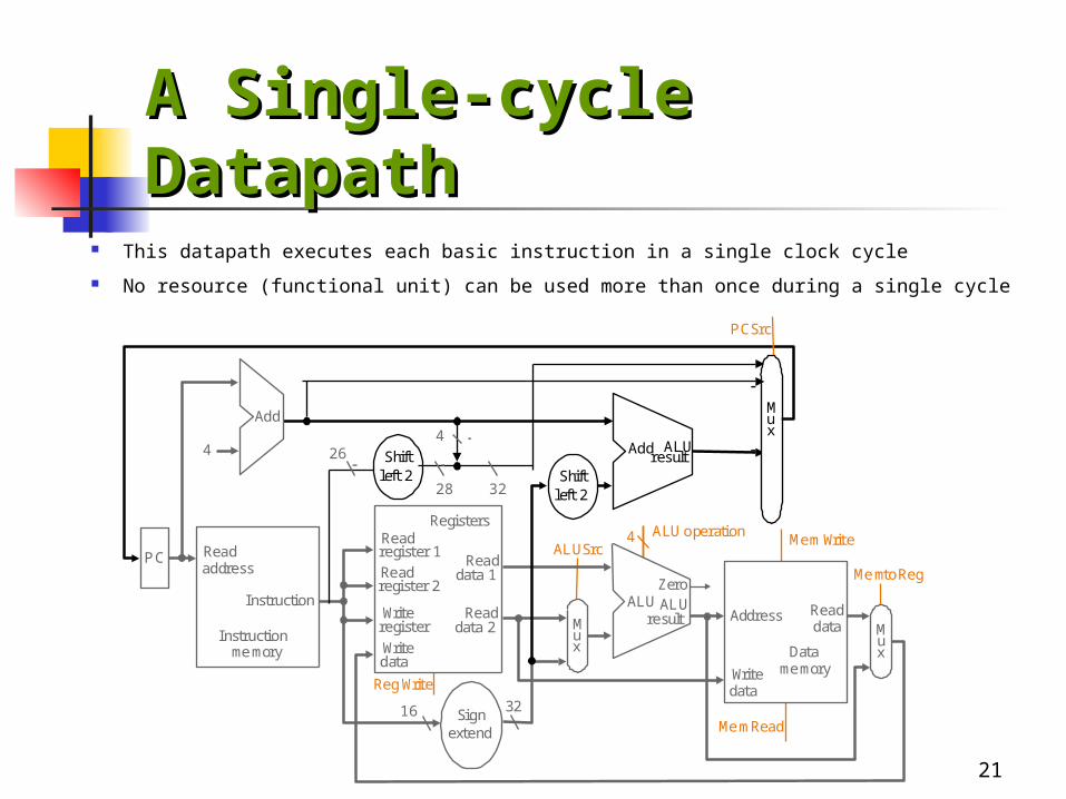
A Single-cycle DatapathA Single-cycle Datapath
This datapath executes each basic instruction in a single clock cycle
No resource (functional unit) can be used more than once during a single cycle
PC
Instructionmemory
Readaddress
Instruction
16 32
Registers
Writeregister
Writedata
Readdata 1
Readdata 2
Readregister 1
Readregister 2
4
Mux
ALU operation4
RegWrite
MemRead
MemWriteALUSrc
MemtoReg
ALUresult
ZeroALU
Datamemory
Address
Writedata
Readdata M
ux
Signextend
Add
Add ALUresult
Mux
PCSrc
Shiftleft 2
Shiftleft 2
264
28 32