Embed Size (px)
Citation preview
Bachelor of Science Thesis in Electrical Engineering
Department of Electrical Engineering, Linköping University, 2018
Design of Bidirectional DC/DC Battery Management System for Electrical Yacht
Daniel Celius Zacharek and Filip Sundqvist
Bachelor of Science Thesis in Electrical Engineering
Design of Bidirectional DC/DC Battery
Management System for Electrical Yacht
Daniel Celius Zacharek and Filip Sundqvist
LiTH-ISY-EX-ET--18/0475--SE
Supervisor:
Tomas Uno Jonsson
ISY, Linköping University
Examiner:
Mark Vesterbacka
ISY, Linköping University
Division of Integrated Circuits and Systems
Department of Electrical Engineering
Linköping University
SE˗581 83 Linköping, Sweden
Copyright 2018 Daniel Celius Zacharek and Filip Sundqvist

iii

iv
Abstract
Electrical vehicles are getting more popular as the technology around batteries and electrical
motors are catching up to the more common combustion engines. Electrical boats are no
exception but there are still a lot of boats using old combustion engines that have a big impact on
the environment. This study aims to deepen the understanding of the integration of electrical
motors into boats by proposing a design of a system using a bidirectional synchronous buck-
boost converter. This converter is designed to handle the power transfer in a dual battery
application, namely consisting of a 12 V battery and a 48 V battery. The converter includes
proposed components, a PCB design, as well as the software that is required for the control of
the power transfer. The results show that the converter design meets specification and, when
using a test-bench, the software is capable of controlling the converter to achieve constant
current and constant voltage in both directions.

v

vi
Acknowledgement
We would like to thank the following people for their support given during our thesis work. Our
supervisor, Tomas Uno Jonsson, for proposing this thesis subject and for his valuable feedback
during this project, as well as his unwavering enthusiasm during our cooperation. Mark
Vesterbacka, our examiner, for his response on our report and presentation. Our opponents
Hassan Moumin and Faris Al-Egli for reviewing the report and providing us with comments and
bringing a discussion during the presentation.

vii
viii
Table of Contents
1 Introduction ................................................................................................................... 12 1.1 Background ............................................................................................................ 12 1.2 Motivation and Purpose ......................................................................................... 13 1.3 Questions and Problems ........................................................................................ 14 1.4 Limitations ............................................................................................................. 14
2 Theory ............................................................................................................................ 15 2.1 DC/DC Converters and PWM ............................................................................... 15
2.1.1 Pulse Width Modulation............................................................................... 15 2.1.2 Generic switch mode converters .................................................................. 16
2.2 MOSFET ............................................................................................................... 23
2.2.1 Design Considerations ................................................................................. 23 2.2.2 Power Losses................................................................................................ 24
2.3 Inductor .................................................................................................................. 26
2.3.1 Design of Inductor ....................................................................................... 26 2.3.2 Power Losses................................................................................................ 27
2.4 Thermal Considerations ......................................................................................... 28 2.5 PV cells .................................................................................................................. 30
2.6 Batteries ................................................................................................................. 30 2.7 Battery Management System ................................................................................. 31
2.8 Driver circuit ......................................................................................................... 32 3 Method ........................................................................................................................... 33
3.1 Pre-study ................................................................................................................ 33 3.1.1 System Overview .......................................................................................... 34
3.1.2 Energy Calculations ..................................................................................... 34 3.1.3 Comparison of Bidirectional Buck-Boost .................................................... 36 3.1.4 Choice of Topology and Specification ......................................................... 37
3.2 Simulation .............................................................................................................. 38 3.2.1 Simulink Simulation ..................................................................................... 38
3.2.2 Multisim Simulation ..................................................................................... 39 3.3 Components and Design ........................................................................................ 39
3.3.1 MOSFET ...................................................................................................... 39 3.3.2 Driver Circuit ............................................................................................... 39 3.3.3 ˗5 V Converter .............................................................................................. 41
3.3.4 Bootstrap ...................................................................................................... 41 3.3.5 Inductor ........................................................................................................ 42 3.3.6 Power Losses................................................................................................ 44 3.3.7 Thermal Considerations ............................................................................... 46
3.3.8 PCB Design .................................................................................................. 48 3.4 Microcontroller and Software ................................................................................ 49
3.4.1 Inputs ............................................................................................................ 49 3.4.2 Outputs ......................................................................................................... 50
3.5 Software Test ......................................................................................................... 50
4 Result .............................................................................................................................. 52 4.1 Final System Design .............................................................................................. 52 4.2 MATLAB Simulink ............................................................................................... 53
4.3 MultiSIM ............................................................................................................... 55 4.4 Efficiency .............................................................................................................. 59 4.5 PCB ........................................................................................................................ 59

ix
4.6 Software Test ......................................................................................................... 59 5 Discussion ....................................................................................................................... 62
5.1 Result...................................................................................................................... 62 5.1.1 Simulations ................................................................................................... 62
5.1.2 Software ........................................................................................................ 62 5.1.3 Efficiency ...................................................................................................... 62 5.1.4 PCB ............................................................................................................... 62
5.2 Method ................................................................................................................... 63 5.2.1 Pre-study ....................................................................................................... 63
5.2.2 Simulation ..................................................................................................... 63 5.2.3 Components and Design ............................................................................... 63 5.2.4 Software test.................................................................................................. 64
5.2.5 Chosen references ......................................................................................... 64 5.3 Ethical Analysis ..................................................................................................... 64
6 Conclusions..................................................................................................................... 66 7 References ....................................................................................................................... 67
8 Appendix......................................................................................................................... 69 8.1 Batteries Used in Project ........................................................................................ 69
8.1.1 12 V lead-acid battery .................................................................................. 69 8.1.2 48 V LiFePo4 battery.................................................................................... 69
8.2 PV panels used in project ....................................................................................... 70

x
List of Figures Figure 1-1 Block diagram of the system .................................................................................................... 13
Figure 2-1 a) Switch-mode DC/DC conversion ......................................................................................... 15
Figure 2-2 PWM ......................................................................................................................................... 16
Figure 2-3 Switching power-pole as the building block ............................................................................. 17
Figure 2-4 Switching power-pole ............................................................................................................... 17
Figure 2-5 Buck circuit ............................................................................................................................... 18
Figure 2-6 Boost circuit .............................................................................................................................. 18
Figure 2-7 An inverting buck-boost circuit ................................................................................................ 19
Figure 2-8 A bidirectional buck-boost converter ....................................................................................... 19
Figure 2-9 First phase of boost mode where s2 is open and s1 is closed ................................................... 20
Figure 2-10 Second phase of boost mode where s2 is closed and s1 is open ............................................. 21
Figure 2-11 Phase one of buck mode where s1 is open and s2 is closed.................................................... 22
Figure 2-12 Phase two of buck mode where s1 is closed and s2 is open ................................................... 23
Figure 2-13 MOSFET turn on characteristics ............................................................................................ 24
Figure 2-14 MOSFET turn off characteristics ............................................................................................ 25
Figure 2-15 The skin depth of different materials at different frequencies by Zureks [CC0], from
Wikimedia Commons ................................................................................................................................. 27
Figure 2-16 Thermal circuit model ............................................................................................................. 29
Figure 2-17 Simplified model of the PV cell ............................................................................................. 30
Figure 2-18 State of charge in a battery, Copyright © 2018 EV Power, Reprinted by permission of EV
Power. ......................................................................................................................................................... 31
Figure 3-1 The steps of the engineering design process ............................................................................. 33
Figure 3-2 System overview ....................................................................................................................... 34
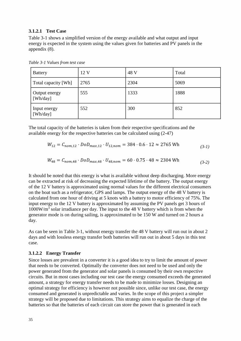
Figure 3-3 Proposed charge schedule where the SoC for the 48 V battery is on the Y-axis and the SoC for
the 12 V battery is on the X-axis ................................................................................................................ 36
Figure 3-4 Four-Switch Noninverting Buck-Boost Converter circuit ........................................................ 37
Figure 3-5 Two-switch bidirectional buck-boost converter ....................................................................... 37
Figure 3-6 Topology simulated in MATLAB Simulink ............................................................................. 38
Figure 3-7 MOSFET simulation test circuit without component values in MultiSIM ............................... 39
Figure 3-8 Heat flow diagram .................................................................................................................... 46
Figure 3-9 Equivalent heat flow circuit ...................................................................................................... 46
Figure 3-10 PCB design for DC/DC converter (in blue square) and BLDC inverter (in grey square) ...... 48
Figure 3-11 Closeup of PCB design for DC/DC converter (left of blue line) ............................................ 49
Figure 3-12 Software test in Simulink ........................................................................................................ 51
Figure 4-1 Converter circuit with capacitor and inductor values ............................................................... 52
Figure 4-2 Inside the driver circuit subsheet with the final decided component values ............................. 52
Figure 4-3 Inside of the ˗5 converter subsheet ........................................................................................... 53
Figure 4-4 Topology simulated with PID in MATLAB Simulink ............................................................. 53
Figure 4-5 Current through inductor with a current reference of 40 A ...................................................... 54
Figure 4-6 Voltage and current charging the 12V battery in MATLAB Simulink .................................... 54
Figure 4-7 Voltage and current charging the 48 V battery in MATLAB Simulink ................................... 55
Figure 4-8 Final circuit for MOSFET simulation with decided values in MultiSIM ................................. 55
Figure 4-9 Gate-source voltage for upper transistor, limit of 3 V and PWM for lower transistor ............. 56
Figure 4-10 VGS for the upper MOSFET during turn on, the PWM signal can also be seen.................... 56
Figure 4-11 VGS for the upper MOSFET during turn off, the PWM signal can also be seen ................... 57
Figure 4-12 The voltage spike due to large dV/dt in upper MOSFET ....................................................... 58
Figure 4-13 The voltage spike due to large dV/dt in lower MOSFET ....................................................... 58
Figure 4-14 3D preview of PCB design ..................................................................................................... 59
Figure 4-15 Step response of constant current regulation during boost mode (1 second per square) ........ 60
Figure 4-16 Step response of constant voltage regulation during boost mode (1 second per square) ........ 60
Figure 4-17 Step response of constant current regulation during buck mode (1 second per square) ......... 61
Figure 4-18 Step response of constant voltage regulation during buck mode (1 second per square) ......... 61
xi
List of Tables
Table 1-1 Table of Abbreviations .................................................................................................. xi Table 3-1 Values from test case .................................................................................................... 35
Table 3-2 Specification for the system ......................................................................................... 38 Table 3-3 Electrical specifications for UCC5390SC .................................................................... 40 Table 3-4 Chosen values for UCC5390SC components ............................................................... 40 Table 3-5 Chosen values for LT1054 circuit components ............................................................ 41 Table 3-6 Dimensions and calculations for selected inductor ferrite core .................................... 43
Table 3-7 Components used during software test ......................................................................... 50
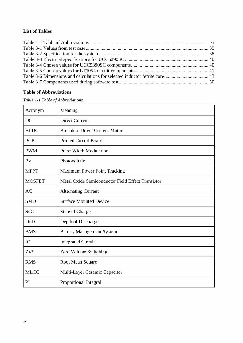
Table of Abbreviations
Table 1-1 Table of Abbreviations
Acronym Meaning
DC Direct Current
BLDC Brushless Direct Current Motor
PCB Printed Circuit Board
PWM Pulse Width Modulation
PV Photovoltaic
MPPT Maximum Power Point Tracking
MOSFET Metal Oxide Semiconductor Field Effect Transistor
AC Alternating Current
SMD Surface Mounted Device
SoC State of Charge
DoD Depth of Discharge
BMS Battery Management System
IC Integrated Circuit
ZVS Zero Voltage Switching
RMS Root Mean Square
MLCC Multi-Layer Ceramic Capacitor
PI Proportional Integral

12
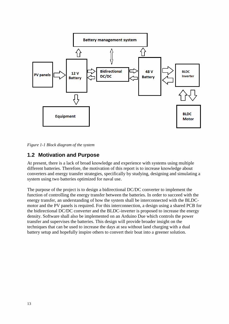
1 Introduction Today the transportation industry is expanding with electric vehicles, but the evolution of
electrical boats and yachts is going much slower. In order to change this trend a project about
updating a yacht from having a fossil fueled petrol engine to a brushless dc-motor (BLDC)
powered by PV panels and regenerative braking is proposed at Linköping University. By
designing a bidirectional buck-boost converter for a dual battery system the goal is to allow
power flow between batteries to minimize the need for battery charging.
1.1 Background
A campaign has been proposed by the current Swedish government that will subsidize
replacing combustion engines with electrical motors hoping to spur many into purchasing an
electrical motor. This campaign is motivated by environmental reasons such as that older
combustion engines release large amounts of hydrocarbons [1].
The electrical system of a yacht, which in most cases run on 12 V batteries, can be difficult to
integrate with an electrical motor system that might use a different voltage or higher current.
At the time of writing there are a few commercially dedicated solutions to replace an old
engine with an electrical motor to update the system. Design of a system for this purpose can
be valuable experience when it comes to future implementations.
The proposed system layout is that the yacht, a 30 feet Comfort will be equipped with two
different PV panels, one horizontal in the front and one with flexible movement in the rear.
The energy storage on the yacht consists of a 12 V lead-acid battery and a 48 V LiFePo
battery. The 12 V battery is charged by the PV panels, which supplies power to the equipment
on the yacht while the 48 V battery is connected to the motor that can both consume and
generate energy while sailing. The two batteries are connected by the bidirectional DC/DC
converter to allow transfer of energy in both directions, a block diagram of the system is
shown in Figure 1-1. The system uses an Arduino Due to provide a battery management
system (BMS) that controls the power flow and makes sure that the batteries are not over-
charged or too deeply discharged. The idea of the BMS is to allow more control of the power
generated by the PV panels and the motor with the goal to provide energy for the yacht to run
at 5 knots for about an hour every day which corresponds to about 1.33 kWh consumption.
13
Figure 1-1 Block diagram of the system
1.2 Motivation and Purpose
At present, there is a lack of broad knowledge and experience with systems using multiple
different batteries. Therefore, the motivation of this report is to increase knowledge about
converters and energy transfer strategies, specifically by studying, designing and simulating a
system using two batteries optimized for naval use.
The purpose of the project is to design a bidirectional DC/DC converter to implement the
function of controlling the energy transfer between the batteries. In order to succeed with the
energy transfer, an understanding of how the system shall be interconnected with the BLDC-
motor and the PV panels is required. For this interconnection, a design using a shared PCB for
the bidirectional DC/DC converter and the BLDC-inverter is proposed to increase the energy
density. Software shall also be implemented on an Arduino Due which controls the power
transfer and supervises the batteries. This design will provide broader insight on the
techniques that can be used to increase the days at sea without land charging with a dual
battery setup and hopefully inspire others to convert their boat into a greener solution.

14
1.3 Questions and Problems
The report aims towards answering the following questions:
How can a bidirectional converter for a dual battery system be designed?
How can the bidirectional converter design be implemented on a PCB?
How can software be implemented to control the power transfer of the system?
How should the software decide when to transfer energy?
With these questions in mind, a suitable method is chosen. The design of the implementation
is decided after simulations of the system. Suggestions for components and thermal
management is provided. Finally, the software will be evaluated using a test-bench.
1.4 Limitations
There are multiple limitations in this project that might affect the result which must be taken
into consideration. First of all, the project time is limited to ten weeks. This means in turn that
some design considerations may be shifted towards simplicity rather than efficiency. Since the
project is funded by a single individual, money and component suppliers are also limitations.
The electronics suppliers are Elfa Distrelec and Mouser. This will limit the choice of
components and increase the importance of thorough simulations placing orders to not waste
money. A third limitation is that the other parts of the system (presented in chapter 3.1.1) need
to work in tandem with our design. Hence these components impact on the whole system must
be considered. Special care is needed since the system is implemented on the same PCB as the
circuit controlling the BLDC motor. The last limitation is the complexity of the software. It
must be able to run on an Arduino Due which is limited in computing power.
15
2 Theory The theory will address the underlying knowledge required with regards to DC/DC converters
and batteries. It aims towards providing a base for the design choices in the method using
previous experience in the field. Since power electronics has a long history of development,
only some of the basics will be covered regarding DC/DC converters, thermal considerations
and pulse width modulation (PWM). An important part of the converter is the use of
transistors and inductors. To understand the operation of photovoltaic (PV) panels and driver
circuits, the basics of their operation is explained.
2.1 DC/DC Converters and PWM
Power converters are an integral part of many electrical systems that require energy transfer
between one voltage level to another, as the voltage required may be different to the voltage
supplied. To achieve energy-efficient conversions, switch-mode conversion is used [2]. The
three generic switch-mode DC/DC converters that will be explained are Buck, Boost and
Buck-Boost DC/DC converters as well as the PWM required to control them. The theory and
equations for PWM and generic switch mode converters are provided by [2] while the theory
for the bidirectional buck-boost converter is provided by [3].
2.1.1 Pulse Width Modulation
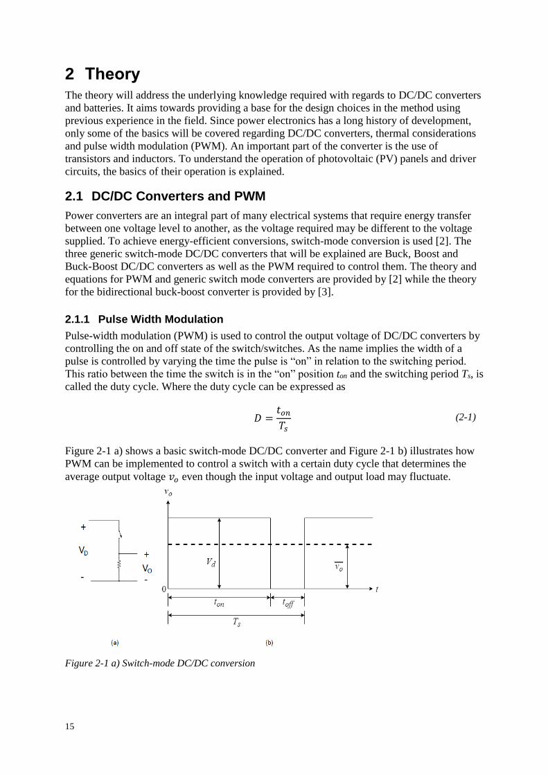
Pulse-width modulation (PWM) is used to control the output voltage of DC/DC converters by
controlling the on and off state of the switch/switches. As the name implies the width of a
pulse is controlled by varying the time the pulse is “on” in relation to the switching period.
This ratio between the time the switch is in the “on” position ton and the switching period Ts, is
called the duty cycle. Where the duty cycle can be expressed as
𝐷 =
𝑡𝑜𝑛
𝑇𝑠
(2-1)
Figure 2-1 a) shows a basic switch-mode DC/DC converter and Figure 2-1 b) illustrates how
PWM can be implemented to control a switch with a certain duty cycle that determines the
average output voltage 𝑣𝑜 even though the input voltage and output load may fluctuate.
Figure 2-1 a) Switch-mode DC/DC conversion
16
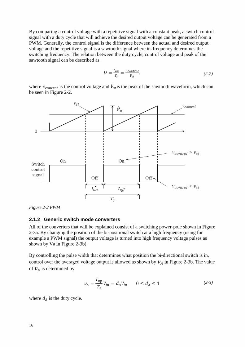
By comparing a control voltage with a repetitive signal with a constant peak, a switch control
signal with a duty cycle that will achieve the desired output voltage can be generated from a
PWM. Generally, the control signal is the difference between the actual and desired output
voltage and the repetitive signal is a sawtooth signal where its frequency determines the
switching frequency. The relation between the duty cycle, control voltage and peak of the
sawtooth signal can be described as
𝐷 =𝑡𝑜𝑛
𝑇𝑠=
𝑣𝑐𝑜𝑛𝑡𝑟𝑜𝑙
𝑉𝑠𝑡.
(2-2)
where 𝑣𝑐𝑜𝑛𝑡𝑟𝑜𝑙 is the control voltage and 𝑠𝑡is the peak of the sawtooth waveform, which can
be seen in Figure 2-2.
Figure 2-2 PWM
2.1.2 Generic switch mode converters
All of the converters that will be explained consist of a switching power-pole shown in Figure
2-3a. By changing the position of the bi-positional switch at a high frequency (using for
example a PWM signal) the output voltage is turned into high frequency voltage pulses as
shown by Va in Figure 2-3b).
By controlling the pulse width that determines what position the bi-directional switch is in,
control over the averaged voltage output is allowed as shown by 𝑣𝐴 in Figure 2-3b. The value
of 𝑣𝐴 is determined by
𝑣𝐴 =
𝑇𝑢𝑝
𝑇𝑠𝑉𝑖𝑛 = 𝑑𝐴𝑉𝑖𝑛 0 ≤ 𝑑𝐴 ≤ 1 (2-3)
where 𝑑𝐴 is the duty cycle.
17
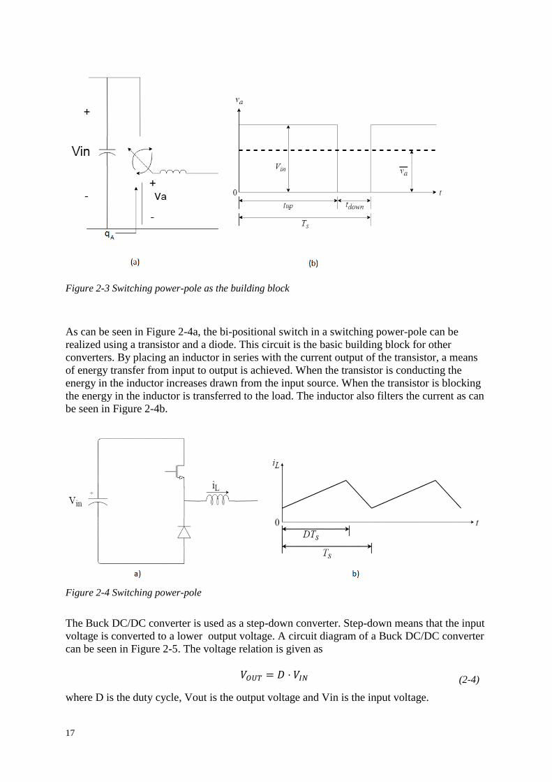
Figure 2-3 Switching power-pole as the building block
As can be seen in Figure 2-4a, the bi-positional switch in a switching power-pole can be
realized using a transistor and a diode. This circuit is the basic building block for other
converters. By placing an inductor in series with the current output of the transistor, a means
of energy transfer from input to output is achieved. When the transistor is conducting the
energy in the inductor increases drawn from the input source. When the transistor is blocking
the energy in the inductor is transferred to the load. The inductor also filters the current as can
be seen in Figure 2-4b.
Figure 2-4 Switching power-pole
The Buck DC/DC converter is used as a step-down converter. Step-down means that the input
voltage is converted to a lower output voltage. A circuit diagram of a Buck DC/DC converter
can be seen in Figure 2-5. The voltage relation is given as
𝑉𝑂𝑈𝑇 = 𝐷 ⋅ 𝑉𝐼𝑁 (2-4)
where D is the duty cycle, Vout is the output voltage and Vin is the input voltage.
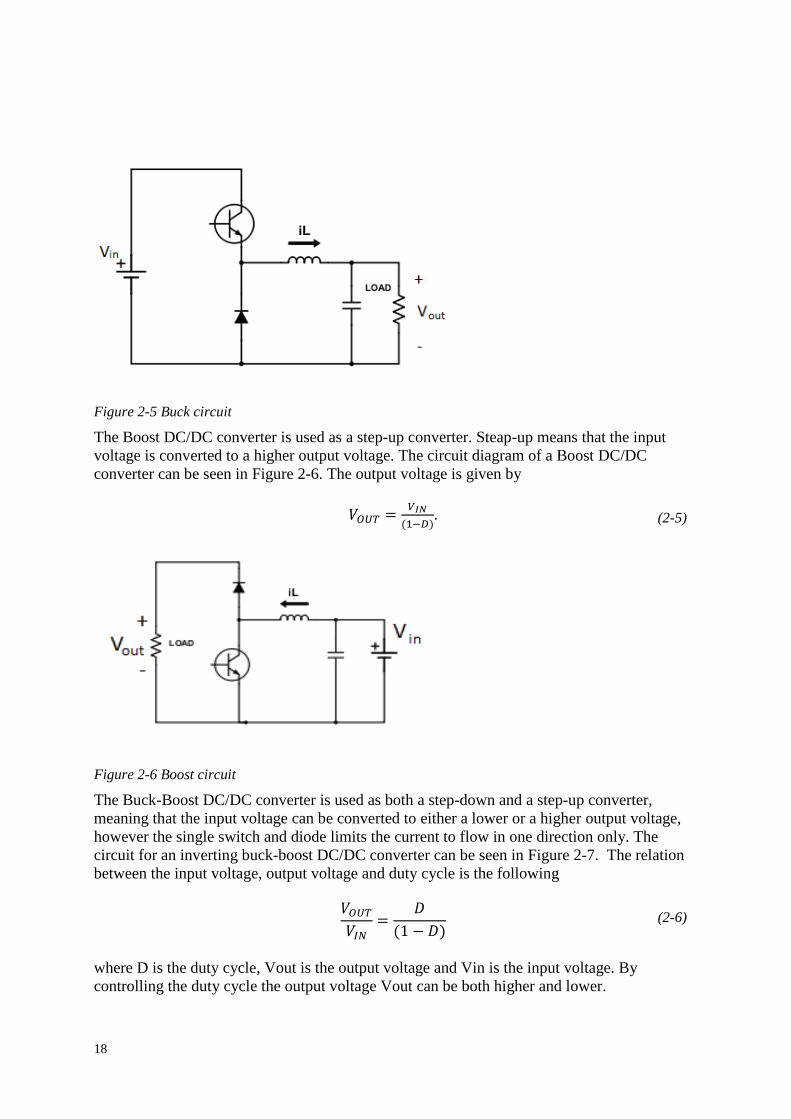
18
Figure 2-5 Buck circuit
The Boost DC/DC converter is used as a step-up converter. Steap-up means that the input
voltage is converted to a higher output voltage. The circuit diagram of a Boost DC/DC
converter can be seen in Figure 2-6. The output voltage is given by
𝑉𝑂𝑈𝑇 =𝑉𝐼𝑁
(1−𝐷). (2-5)
Figure 2-6 Boost circuit
The Buck-Boost DC/DC converter is used as both a step-down and a step-up converter,
meaning that the input voltage can be converted to either a lower or a higher output voltage,
however the single switch and diode limits the current to flow in one direction only. The
circuit for an inverting buck-boost DC/DC converter can be seen in Figure 2-7. The relation
between the input voltage, output voltage and duty cycle is the following
𝑉𝑂𝑈𝑇
𝑉𝐼𝑁=
𝐷
(1 − 𝐷)
(2-6)
where D is the duty cycle, Vout is the output voltage and Vin is the input voltage. By
controlling the duty cycle the output voltage Vout can be both higher and lower.
19
Figure 2-7 An inverting buck-boost circuit
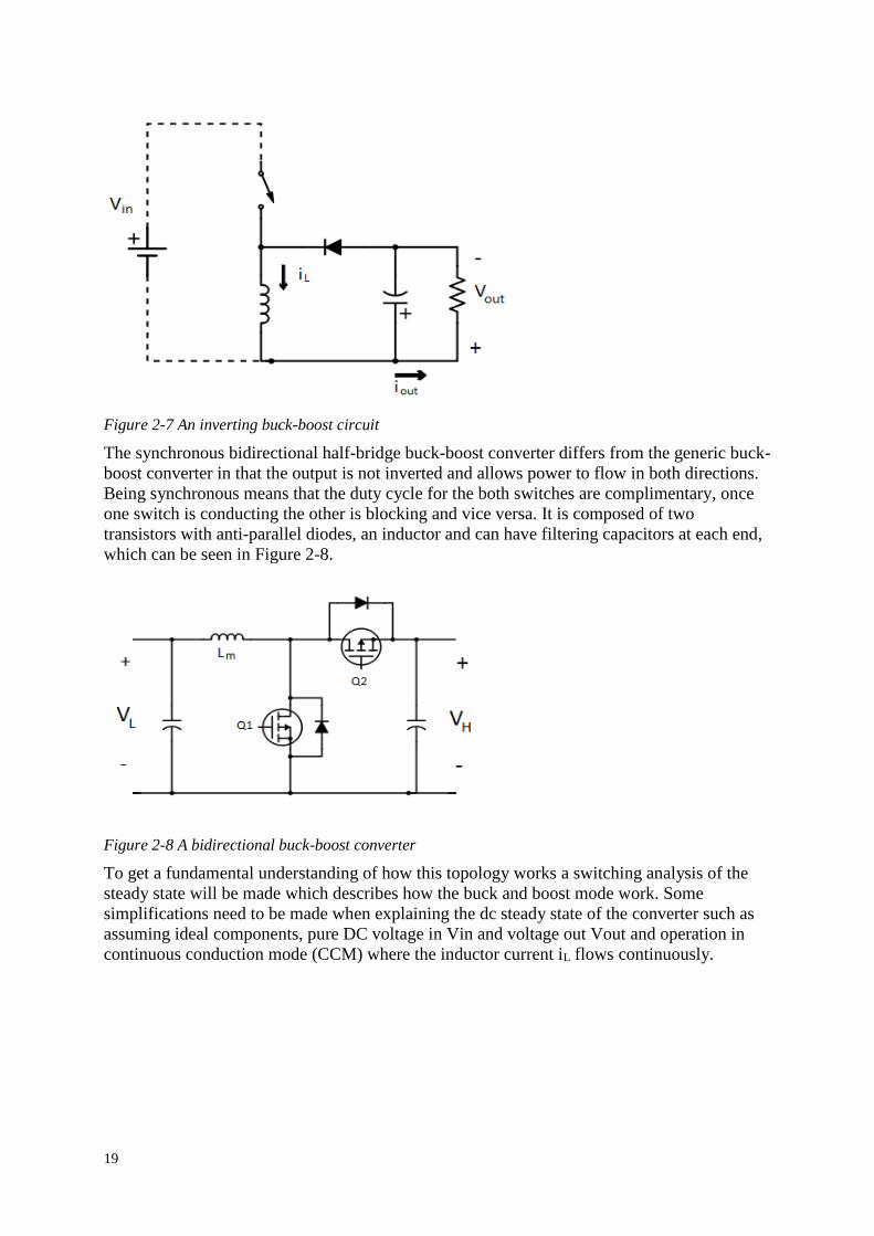
The synchronous bidirectional half-bridge buck-boost converter differs from the generic buck-
boost converter in that the output is not inverted and allows power to flow in both directions.
Being synchronous means that the duty cycle for the both switches are complimentary, once
one switch is conducting the other is blocking and vice versa. It is composed of two
transistors with anti-parallel diodes, an inductor and can have filtering capacitors at each end,
which can be seen in Figure 2-8.
Figure 2-8 A bidirectional buck-boost converter
To get a fundamental understanding of how this topology works a switching analysis of the
steady state will be made which describes how the buck and boost mode work. Some
simplifications need to be made when explaining the dc steady state of the converter such as
assuming ideal components, pure DC voltage in Vin and voltage out Vout and operation in
continuous conduction mode (CCM) where the inductor current iL flows continuously.
20
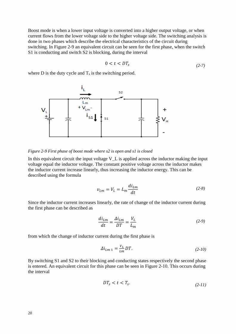
Boost mode is when a lower input voltage is converted into a higher output voltage, or when
current flows from the lower voltage side to the higher voltage side. The switching analysis is
done in two phases which describe the electrical characteristics of the circuit during
switching. In Figure 2-9 an equivalent circuit can be seen for the first phase, when the switch
S1 is conducting and switch S2 is blocking, during the interval
0 < 𝑡 < 𝐷𝑇𝑠 (2-7)
where D is the duty cycle and Ts is the switching period.
Figure 2-9 First phase of boost mode where s2 is open and s1 is closed
In this equivalent circuit the input voltage V_L is applied across the inductor making the input
voltage equal the inductor voltage. The constant positive voltage across the inductor makes
the inductor current increase linearly, thus increasing the inductor energy. This can be
described using the formula
𝑣𝐿𝑚 = 𝑉𝐿 = 𝐿𝑚
𝑑𝑖𝐿𝑚
𝑑𝑡 (2-8)
Since the inductor current increases linearly, the rate of change of the inductor current during
the first phase can be described as
𝑑𝑖𝐿𝑚
𝑑𝑡=
𝛥𝑖𝐿𝑚
𝐷𝑇=
𝑉𝐿
𝐿𝑚 (2-9)
from which the change of inductor current during the first phase is
𝛥𝑖𝐿𝑚 1 =𝑉𝐿
𝐿𝑚𝐷𝑇.
(2-10)
By switching S1 and S2 to their blocking and conducting states respectively the second phase
is entered. An equivalent circuit for this phase can be seen in Figure 2-10. This occurs during
the interval
𝐷𝑇𝑠 < 𝑡 < 𝑇𝑠. (2-11)
21
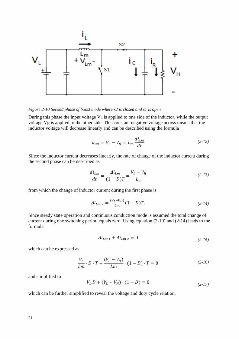
Figure 2-10 Second phase of boost mode where s2 is closed and s1 is open
During this phase the input voltage VL is applied to one side of the inductor, while the output
voltage VH is applied to the other side. This constant negative voltage across means that the
inductor voltage will decrease linearly and can be described using the formula
𝑣𝐿𝑚 = 𝑉𝐿 − 𝑉𝐻 = 𝐿𝑚
𝑑𝑖𝐿𝑚
𝑑𝑡
(2-12)
Since the inductor current decreases linearly, the rate of change of the inductor current during
the second phase can be described as
𝑑𝑖𝐿𝑚
𝑑𝑡=
𝛥𝑖𝐿𝑚
(1 − 𝐷)𝑇=
𝑉𝐿 − 𝑉𝐻
𝐿𝑚
(2-13)
from which the change of inductor current during the first phase is
𝛥𝑖𝐿𝑚 2 =(𝑉𝐿−𝑉𝐻)
𝐿𝑚(1 − 𝐷)𝑇.
(2-14)
Since steady state operation and continuous conduction mode is assumed the total change of
current during one switching period equals zero. Using equation (2-10) and (2-14) leads to the
formula
𝛥𝑖𝐿𝑚 1 + 𝛥𝑖𝐿𝑚 2 = 0
(2-15)
which can be expressed as
𝑉𝐿
𝐿𝑚⋅ 𝐷 ⋅ 𝑇 +
(𝑉𝐿 − 𝑉𝐻)
𝐿𝑚⋅ (1 − 𝐷) ⋅ 𝑇 = 0
(2-16)
and simplified to
𝑉𝐿⋅𝐷 + (𝑉𝐿 − 𝑉𝐻) ⋅ (1 − 𝐷) = 0
(2-17)
which can be further simplified to reveal the voltage and duty cycle relation,
22
𝑉𝐻 =1
1−𝐷⋅ 𝑉𝐿.
(2-18)
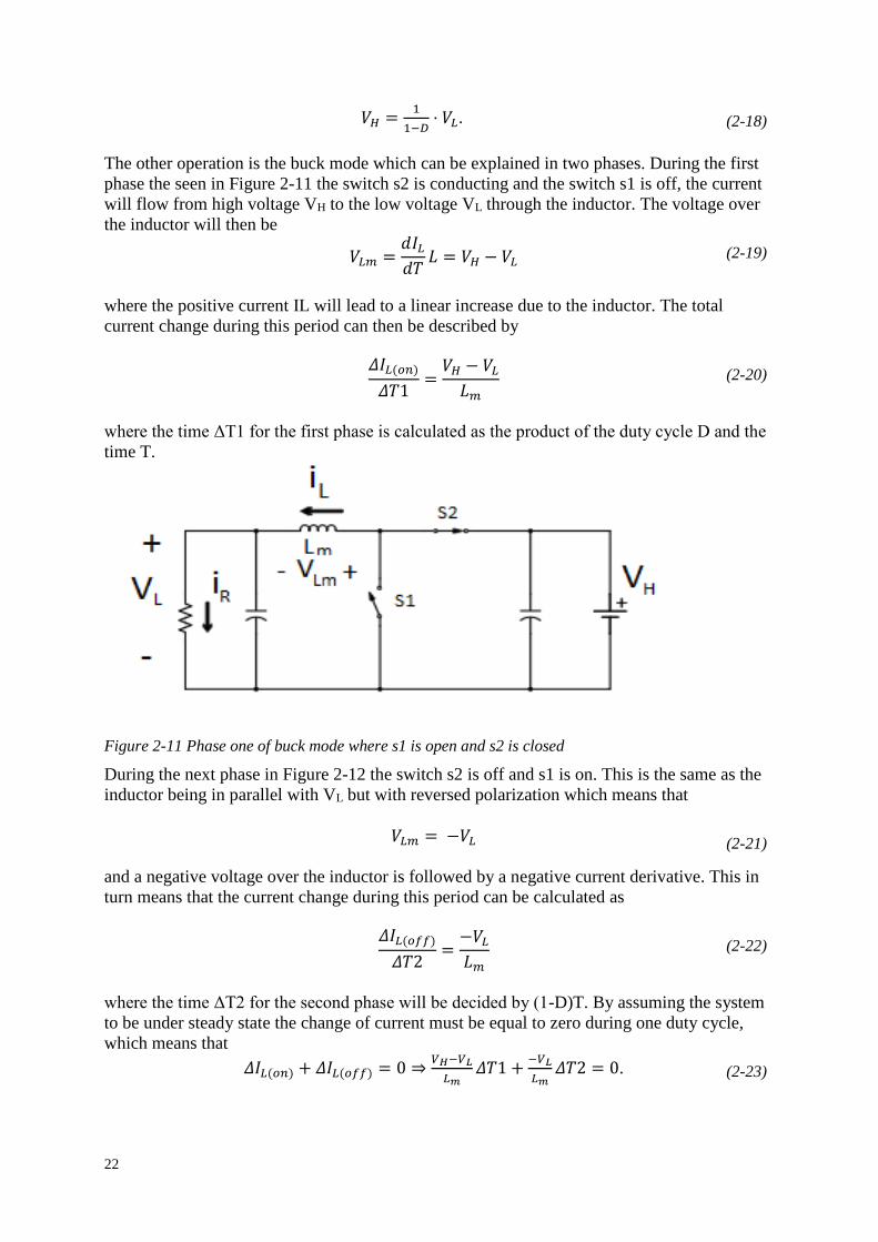
The other operation is the buck mode which can be explained in two phases. During the first
phase the seen in Figure 2-11 the switch s2 is conducting and the switch s1 is off, the current
will flow from high voltage VH to the low voltage VL through the inductor. The voltage over
the inductor will then be
𝑉𝐿𝑚 =
𝑑𝐼𝐿
𝑑𝑇𝐿 = 𝑉𝐻 − 𝑉𝐿
(2-19)
where the positive current IL will lead to a linear increase due to the inductor. The total
current change during this period can then be described by
𝛥𝐼𝐿(𝑜𝑛)
𝛥𝑇1=
𝑉𝐻 − 𝑉𝐿
𝐿𝑚
(2-20)
where the time ΔT1 for the first phase is calculated as the product of the duty cycle D and the
time T.
Figure 2-11 Phase one of buck mode where s1 is open and s2 is closed
During the next phase in Figure 2-12 the switch s2 is off and s1 is on. This is the same as the
inductor being in parallel with VL but with reversed polarization which means that
𝑉𝐿𝑚 = −𝑉𝐿
(2-21)
and a negative voltage over the inductor is followed by a negative current derivative. This in
turn means that the current change during this period can be calculated as
𝛥𝐼𝐿(𝑜𝑓𝑓)
𝛥𝑇2=
−𝑉𝐿
𝐿𝑚
(2-22)
where the time ΔT2 for the second phase will be decided by (1-D)T. By assuming the system
to be under steady state the change of current must be equal to zero during one duty cycle,
which means that
𝛥𝐼𝐿(𝑜𝑛) + 𝛥𝐼𝐿(𝑜𝑓𝑓) = 0 ⇒𝑉𝐻−𝑉𝐿
𝐿𝑚𝛥𝑇1 +
−𝑉𝐿
𝐿𝑚𝛥𝑇2 = 0. (2-23)
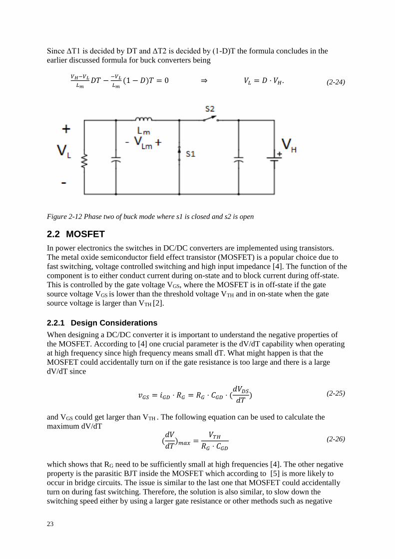
23
Since ΔT1 is decided by DT and ΔT2 is decided by (1-D)T the formula concludes in the
earlier discussed formula for buck converters being
𝑉𝐻−𝑉𝐿
𝐿𝑚𝐷𝑇 −
−𝑉𝐿
𝐿𝑚(1 − 𝐷)𝑇 = 0 ⇒ 𝑉𝐿 = 𝐷 ⋅ 𝑉𝐻. (2-24)
Figure 2-12 Phase two of buck mode where s1 is closed and s2 is open
2.2 MOSFET
In power electronics the switches in DC/DC converters are implemented using transistors.
The metal oxide semiconductor field effect transistor (MOSFET) is a popular choice due to
fast switching, voltage controlled switching and high input impedance [4]. The function of the
component is to either conduct current during on-state and to block current during off-state.
This is controlled by the gate voltage VGS, where the MOSFET is in off-state if the gate
source voltage VGS is lower than the threshold voltage VTH and in on-state when the gate
source voltage is larger than VTH [2].
2.2.1 Design Considerations
When designing a DC/DC converter it is important to understand the negative properties of
the MOSFET. According to [4] one crucial parameter is the dV/dT capability when operating
at high frequency since high frequency means small dT. What might happen is that the
MOSFET could accidentally turn on if the gate resistance is too large and there is a large
dV/dT since
𝑣𝐺𝑆 = 𝑖𝐺𝐷 ⋅ 𝑅𝐺 = 𝑅𝐺 ⋅ 𝐶𝐺𝐷 ⋅ (
𝑑𝑉𝐷𝑆
𝑑𝑇) (2-25)
and VGS could get larger than VTH . The following equation can be used to calculate the
maximum dV/dT
(𝑑𝑉
𝑑𝑇)𝑚𝑎𝑥 =
𝑉𝑇𝐻
𝑅𝐺 ⋅ 𝐶𝐺𝐷
(2-26)
which shows that RG need to be sufficiently small at high frequencies [4]. The other negative
property is the parasitic BJT inside the MOSFET which according to [5] is more likely to
occur in bridge circuits. The issue is similar to the last one that MOSFET could accidentally
turn on during fast switching. Therefore, the solution is also similar, to slow down the
switching speed either by using a larger gate resistance or other methods such as negative
24
bias. This is why the value for the external gate resistance needs to be selected carefully since
it should neither be too big or too small.
When designing a circuit containing MOSFETs on a PCB for high frequency applications it is
important to think about the stray inductances. Parasitic inductance will appear both from the
MOSFET packaging but also in the capacitors and from the PCB traces. What can appear is
that the MOSFET is overstressed due to high VDS if the stray inductances are too large since
𝑉𝐷𝑆(𝑡𝑢𝑟𝑛−𝑜𝑓𝑓) = 𝑉𝐷 + 𝐿
𝑑𝐼
𝑑𝑇 (2-27)
where a VDS overvoltage can damage the MOSFET.
2.2.2 Power Losses
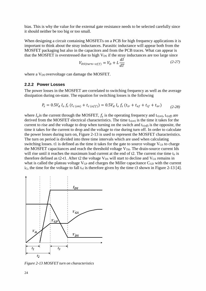
The power losses in the MOSFET are correlated to switching frequency as well as the average
dissipation during on-state. The equation for switching losses is the following
𝑃𝑠 = 0.5𝑉𝑑 𝐼𝑜 𝑓𝑠 (𝑡𝑐 (𝑜𝑛) + 𝑡𝑐 (𝑜𝑓𝑓)) = 0.5𝑉𝑑 𝐼𝑜 𝑓𝑠 (𝑡𝑖𝑟 + 𝑡𝑣𝑓 + 𝑡𝑖𝑓 + 𝑡𝑣𝑟)
(2-28)
where 𝐼𝑜is the current through the MOSFET, 𝑓𝑠 is the operating frequency and tc(on), tc(off) are
derived from the MOSFET electrical characteristics. The time tc(on) is the time it takes for the
current to rise and the voltage to drop when turning on the switch and tc(off) is the opposite, the
time it takes for the current to drop and the voltage to rise during turn off. In order to calculate
the power losses during turn on, Figure 2-13 is used to represent the MOSFET characteristics.
The turn on period is divided into three time intervals which are used when calculating
switching losses. t1 is defined as the time it takes for the gate to source voltage VGS to charge
the MOSFET capacitances and reach the threshold voltage VTH. The drain-source current Ids
will rise until it reaches the maximum load current at the end of t2. The current rise time tir is
therefore defined as t2-t1. After t2 the voltage VDS will start to decline and VGS remains in
what is called the plateau voltage VGP and charges the Miller capacitance CGD with the current
iG, the time for the voltage to fall tvf is therefore given by the time t3 shown in Figure 2-13 [4].
Figure 2-13 MOSFET turn on characteristics
25
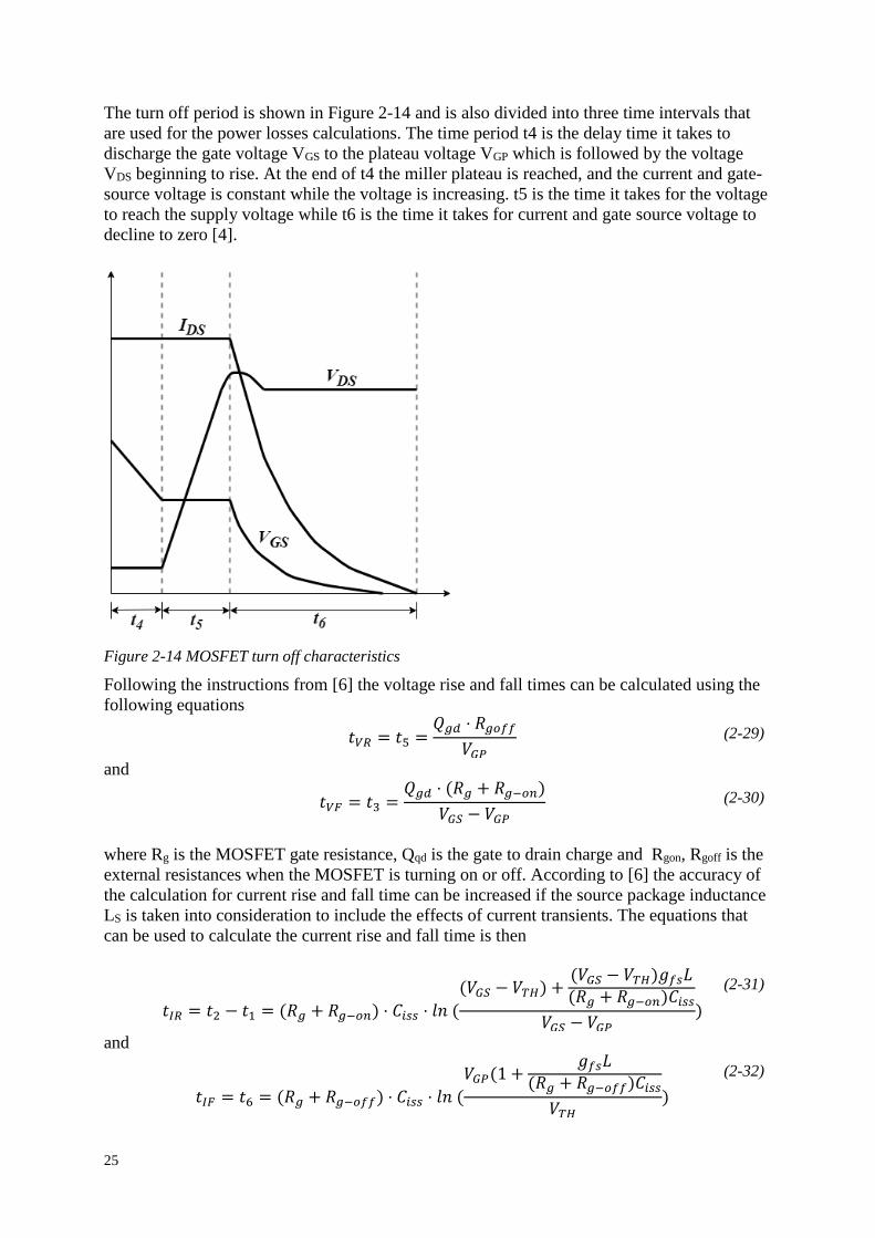
The turn off period is shown in Figure 2-14 and is also divided into three time intervals that
are used for the power losses calculations. The time period t4 is the delay time it takes to
discharge the gate voltage VGS to the plateau voltage VGP which is followed by the voltage
VDS beginning to rise. At the end of t4 the miller plateau is reached, and the current and gate-
source voltage is constant while the voltage is increasing. t5 is the time it takes for the voltage
to reach the supply voltage while t6 is the time it takes for current and gate source voltage to
decline to zero [4].
Figure 2-14 MOSFET turn off characteristics
Following the instructions from [6] the voltage rise and fall times can be calculated using the
following equations
𝑡𝑉𝑅 = 𝑡5 =
𝑄𝑔𝑑 ⋅ 𝑅𝑔𝑜𝑓𝑓
𝑉𝐺𝑃 (2-29)
and
𝑡𝑉𝐹 = 𝑡3 =
𝑄𝑔𝑑 ⋅ (𝑅𝑔 + 𝑅𝑔−𝑜𝑛)
𝑉𝐺𝑆 − 𝑉𝐺𝑃 (2-30)
where Rg is the MOSFET gate resistance, Qqd is the gate to drain charge and Rgon, Rgoff is the
external resistances when the MOSFET is turning on or off. According to [6] the accuracy of
the calculation for current rise and fall time can be increased if the source package inductance
LS is taken into consideration to include the effects of current transients. The equations that
can be used to calculate the current rise and fall time is then
𝑡𝐼𝑅 = 𝑡2 − 𝑡1 = (𝑅𝑔 + 𝑅𝑔−𝑜𝑛) ⋅ 𝐶𝑖𝑠𝑠 ⋅ 𝑙𝑛 (
(𝑉𝐺𝑆 − 𝑉𝑇𝐻) +(𝑉𝐺𝑆 − 𝑉𝑇𝐻)𝑔𝑓𝑠𝐿(𝑅𝑔 + 𝑅𝑔−𝑜𝑛)𝐶𝑖𝑠𝑠
𝑉𝐺𝑆 − 𝑉𝐺𝑃)
(2-31)
and
𝑡𝐼𝐹 = 𝑡6 = (𝑅𝑔 + 𝑅𝑔−𝑜𝑓𝑓) ⋅ 𝐶𝑖𝑠𝑠 ⋅ 𝑙𝑛 (
𝑉𝐺𝑃(1 +𝑔𝑓𝑠𝐿
(𝑅𝑔 + 𝑅𝑔−𝑜𝑓𝑓)𝐶𝑖𝑠𝑠
𝑉𝑇𝐻)
(2-32)

26
where Ciss is the input capacitance consisting of CGS and CGD, gfs is the transconductance and
VTH is the threshold voltage. This concludes the times needed for calculation the switching
losses for the MOSFET. The power losses from the average dissipation during on-state for a
DC/DC converter is calculated with the equation
𝑃𝑜𝑛 = 𝑉𝑜𝑛 𝐼𝑜
𝑡𝑜𝑛
𝑇𝑠= 𝑟𝑜𝑛𝐼𝑜𝑛
2𝑡𝑜𝑛
𝑇𝑠 (2-33)
where the time 𝑡𝑜𝑛
𝑇𝑠is the same as the duty cycle 𝐷 and 𝑟𝑜𝑛,𝐼𝑜𝑛 is the drain-source resistance
and current,𝑅𝐷𝑆and 𝐼𝐷𝑆 during on-state [5].
2.3 Inductor
When designing a DC/DC converter it is important to consider the design of an inductor as
well since inductors are not widely commercially available. This is because they are most
often designed for specific applications.
2.3.1 Design of Inductor
In suggested design calculations from Texas Instruments [7] the following equations can be
used to select appropriate inductor with an inductance L,
𝐿 >
𝑉𝑜𝑢𝑡 ⋅ (𝑉𝑖𝑛𝑚𝑎𝑥 − 𝑉𝑜𝑢𝑡)
𝐾𝑖𝑛𝑑 ⋅ 𝐹𝑠𝑤 ⋅ 𝑉𝑖𝑛𝑚𝑎𝑥 ⋅ 𝐼𝑜𝑢𝑡 (2-34)
for a buck mode converter and
𝐿 >
𝑉𝑖𝑛𝑚𝑖𝑛2 ⋅ (𝑉𝑜𝑢𝑡 − 𝑉𝑖𝑛𝑚𝑖𝑛)
𝐾𝑖𝑛𝑑 ⋅ 𝐹𝑠𝑤 ⋅ 𝐼𝑜𝑢𝑡 ⋅ 𝑉𝑜𝑢𝑡2
(2-35)
for boost mode, where Vinmax is the maximum input voltage, Vout is the output voltage, Iout is
the rated output current, Fsw is the switching frequency and Kind is the maximum current
ripple. The largest value of these inductances is selected.
When selecting a core there are two major classes, ferrites and alloys. Due to small eddy
current losses ferrite cores are a good choice at frequencies higher than 10 kHz but has lower
saturation flux density while alloy cores have higher saturation flux density but suffers from
higher eddy current losses at higher frequencies. The relationship between flux density B, flux
𝛷, core cross-section area Ae can be seen as
𝐵 =
𝛷
𝐴𝑒=
𝑁 ⋅ 𝐼
𝐴𝑒 ⋅ (𝑅𝑔𝑎𝑝 + 𝑅𝑐𝑜𝑟𝑒) (2-36)
where the reluctance Rgap will get bigger with a larger air gap. This results in a limitation to
the magnetic flux being
𝛷 =
𝐵
𝐴𝑒 (2-37)
which limits the amount of turns N by a maximum
27
𝑁 =
𝛷 ⋅ 𝑅𝑡𝑜𝑡
𝐼 (2-38)
and with the decided amount of turns, the inductor value of L can be calculated by
𝐿 =
𝑁2
𝑅𝑡𝑜𝑡 [5]. (2-39)
2.3.2 Power Losses
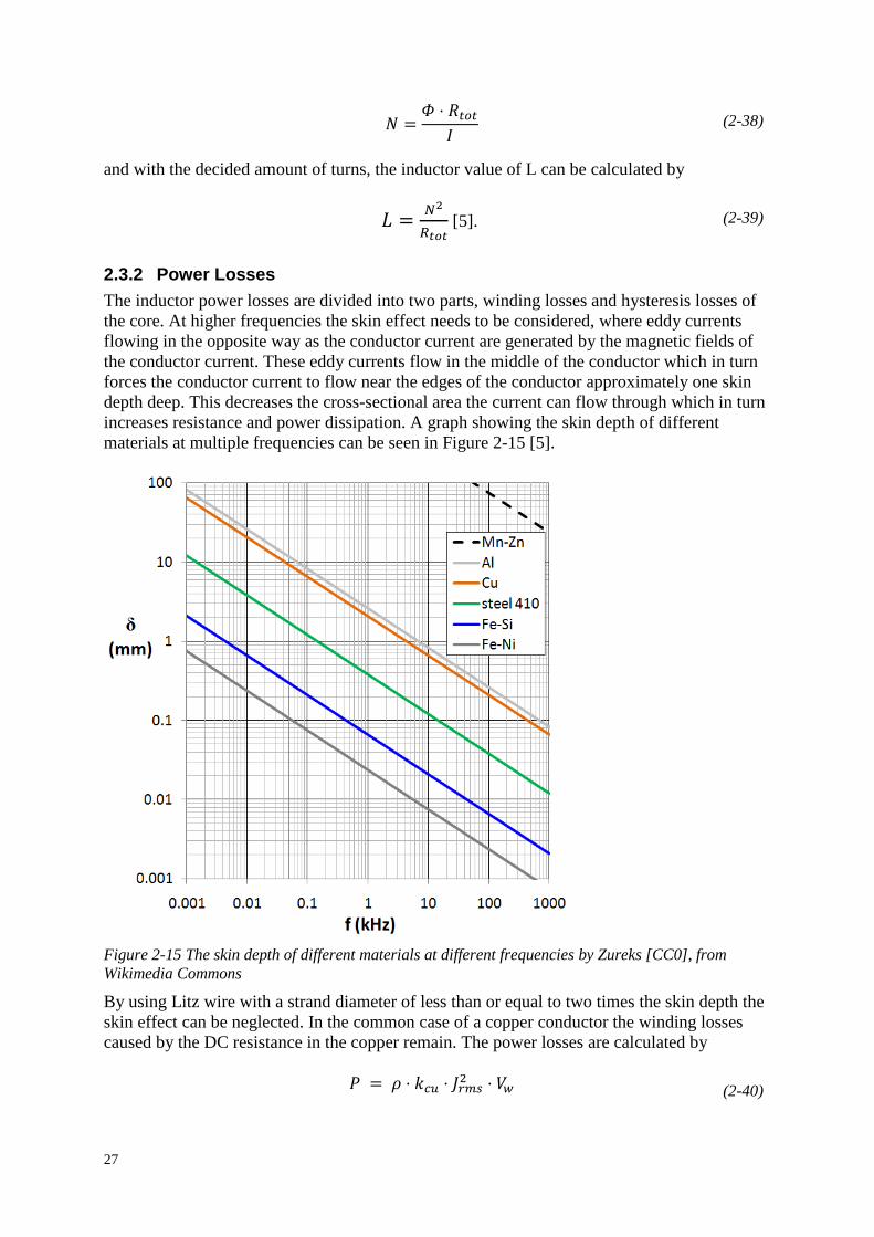
The inductor power losses are divided into two parts, winding losses and hysteresis losses of
the core. At higher frequencies the skin effect needs to be considered, where eddy currents
flowing in the opposite way as the conductor current are generated by the magnetic fields of
the conductor current. These eddy currents flow in the middle of the conductor which in turn
forces the conductor current to flow near the edges of the conductor approximately one skin
depth deep. This decreases the cross-sectional area the current can flow through which in turn
increases resistance and power dissipation. A graph showing the skin depth of different
materials at multiple frequencies can be seen in Figure 2-15 [5].
Figure 2-15 The skin depth of different materials at different frequencies by Zureks [CC0], from
Wikimedia Commons
By using Litz wire with a strand diameter of less than or equal to two times the skin depth the
skin effect can be neglected. In the common case of a copper conductor the winding losses
caused by the DC resistance in the copper remain. The power losses are calculated by
𝑃 = 𝜌 ⋅ 𝑘𝑐𝑢 ⋅ 𝐽𝑟𝑚𝑠2 ⋅ 𝑉𝑤 (2-40)
28
where ρ is the resistivity of copper, kcu is called the fill factor given by, Jrms is the current
density and Vw is the total winding volume given by core dimensions [5]. To minimize these
power losses the design of the conductor must be taken into consideration. If a Litz wire with
multiple strands is used it is possible control the total cross section area of the copper wire Acu
since
𝐴𝑐𝑢 = 𝐴𝑧 ⋅ 𝑧 (2-41)
where Az is the strand cross section area and z is the amounts of Litz strands. By changing the
area Acu it is possible to decrease the current density Jrms is given as
𝐽𝑟𝑚𝑠 =
𝐼𝑅𝑀𝑆
𝐴𝐶𝑈 (2-42)
but at the same time increasing the fill factor kcu since
𝑘𝑐𝑢 =
𝑁 ⋅ 𝐴𝑐𝑢
𝐴𝑤
(2-43)
which gives the designer the possibility to decrease the power losses. It is also important to
have a sufficiently large Acu for high current applications [5].
The hysteresis losses are based on the magnetic characteristics of the core material which
theory will not be provided. The value Pv can usually be found in the datasheet for the core
material where Pv is based on the frequency f of the system and the AC field flux density .
The hysteresis power losses are then calculated by
𝑃𝑐𝑜𝑟𝑒 = 𝑉𝑒 ⋅ 𝑃𝑣 (2-44)
where Ve is the total magnetic core volume given in mm3.
2.4 Thermal Considerations
One of the most important parameters for a power electronics system is the efficiency. The
system should optimally be designed to have as little power losses as possible. The efficiency
is in general given by
𝜂 =
𝑃𝑂𝑈𝑇
𝑃𝐼𝑁
(2-45)
where ɳ is usually given in percent. The converter is very dependent on power losses in the
system since it will affect the layout and the need for cooling. The two big contributors of
power losses are usually the transistors and the inductors due to conduction and switching
losses.
Thermal considerations are necessary since power electronic components suffer detrimental
characteristics if internal temperatures rise. For example, increasing the junction temperature
of a MOSFET increases the on-state resistance significantly, which in turn leads to higher
power dissipation in these power semiconductors [5].
When considering the thermal properties of a system, the worst-case junction temperature
needs to be specified. In order to have a design intended for high reliability, having a worst-
29
case junction temperature of 20 to 40 below 125 is recommended. It should be not be
noted that some components can operate above 200 , however the performance and lifetime
may be poor. The thermal layout is something to be considered at an early stage of system
design since size, weight and temperature of surrounding components of the system are
affected by the chosen cooling solution [5]. In an energy dense system, using surface-mount
devices (SMD) close together to minimize stray inductance, the heatsink can be mounted on
the opposite side of the components on the PCB. The heatsink is connected to the power
components by vias through the pcb that will conduct the power dissipated while providing
some insulation to the other components on the PCB.
The location where the system is placed is also of importance, since heatsinks can be very
large compared to PCBs. The fins of the heatsinks needs to be positioned vertically in the case
where no fan is present, for natural convection of the air to function optimally. The ambient
temperature is also a design input that depends on the location of the system [5].
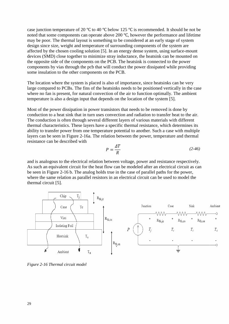
Most of the power dissipation in power transistors that needs to be removed is done by
conduction to a heat sink that in turn uses convection and radiation to transfer heat to the air.
The conduction is often through several different layers of various materials with different
thermal characteristics. These layers have a specific thermal resistance, which determines its
ability to transfer power from one temperature potential to another. Such a case with multiple
layers can be seen in Figure 2-16a. The relation between the power, temperature and thermal
resistance can be described with
𝑃 =
𝛥𝑇
𝑅 (2-46)
and is analogous to the electrical relation between voltage, power and resistance respectively.
As such an equivalent circuit for the heat flow can be modeled after an electrical circuit as can
be seen in Figure 2-16 b. The analog holds true in the case of parallel paths for the power,
where the same relation as parallel resistors in an electrical circuit can be used to model the
thermal circuit [5].
Figure 2-16 Thermal circuit model
30
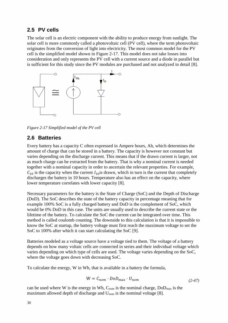
2.5 PV cells
The solar cell is an electric component with the ability to produce energy from sunlight. The
solar cell is more commonly called a photovoltaic cell (PV cell), where the term photovoltaic
originates from the conversion of light into electricity. The most common model for the PV
cell is the simplified model shown in Figure 2-17. This model does not take losses into
consideration and only represents the PV cell with a current source and a diode in parallel but
is sufficient for this study since the PV modules are purchased and not analyzed in detail [8].
Figure 2-17 Simplified model of the PV cell
2.6 Batteries
Every battery has a capacity C often expressed in Ampere hours, Ah, which determines the
amount of charge that can be stored in a battery. The capacity is however not constant but
varies depending on the discharge current. This means that if the drawn current is larger, not
as much charge can be extracted from the battery. That is why a nominal current is needed
together with a nominal capacity in order to ascertain the relevant properties. For example,
𝐶10 is the capacity when the current 𝐼10is drawn, which in turn is the current that completely
discharges the battery in 10 hours. Temperature also has an effect on the capacity, where
lower temperature correlates with lower capacity [8].
Necessary parameters for the battery is the State of Charge (SoC) and the Depth of Discharge
(DoD). The SoC describes the state of the battery capacity in percentage meaning that for
example 100% SoC is a fully charged battery and DoD is the complement of SoC, which
would be 0% DoD in this case. The units are usually used to describe the current state or the
lifetime of the battery. To calculate the SoC the current can be integrated over time. This
method is called coulomb counting. The downside to this calculation is that it is impossible to
know the SoC at startup, the battery voltage must first reach the maximum voltage to set the
SoC to 100% after which it can start calculating the SoC [9].
Batteries modeled as a voltage source have a voltage tied to them. The voltage of a battery
depends on how many voltaic cells are connected in series and their individual voltage which
varies depending on which type of cells are used. The voltage varies depending on the SoC,
where the voltage goes down with decreasing SoC.
To calculate the energy, W in Wh, that is available in a battery the formula,
W = 𝐶𝑛𝑜𝑚 ⋅ 𝐷𝑜𝐷𝑚𝑎𝑥 ⋅ 𝑈𝑛𝑜𝑚 (2-47)
can be used where W is the energy in Wh, Cnom is the nominal charge, DoDmax is the
maximum allowed depth of discharge and Unom is the nominal voltage [8].
31
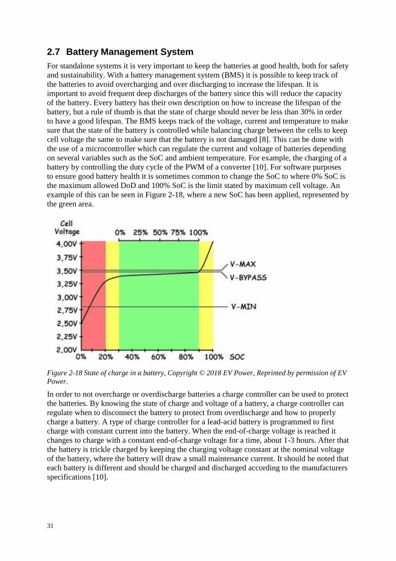
2.7 Battery Management System
For standalone systems it is very important to keep the batteries at good health, both for safety
and sustainability. With a battery management system (BMS) it is possible to keep track of
the batteries to avoid overcharging and over discharging to increase the lifespan. It is
important to avoid frequent deep discharges of the battery since this will reduce the capacity
of the battery. Every battery has their own description on how to increase the lifespan of the
battery, but a rule of thumb is that the state of charge should never be less than 30% in order
to have a good lifespan. The BMS keeps track of the voltage, current and temperature to make
sure that the state of the battery is controlled while balancing charge between the cells to keep
cell voltage the same to make sure that the battery is not damaged [8]. This can be done with
the use of a microcontroller which can regulate the current and voltage of batteries depending
on several variables such as the SoC and ambient temperature. For example, the charging of a
battery by controlling the duty cycle of the PWM of a converter [10]. For software purposes
to ensure good battery health it is sometimes common to change the SoC to where 0% SoC is
the maximum allowed DoD and 100% SoC is the limit stated by maximum cell voltage. An
example of this can be seen in Figure 2-18, where a new SoC has been applied, represented by
the green area.
Figure 2-18 State of charge in a battery, Copyright © 2018 EV Power, Reprinted by permission of EV
Power.
In order to not overcharge or overdischarge batteries a charge controller can be used to protect
the batteries. By knowing the state of charge and voltage of a battery, a charge controller can
regulate when to disconnect the battery to protect from overdischarge and how to properly
charge a battery. A type of charge controller for a lead-acid battery is programmed to first
charge with constant current into the battery. When the end-of-charge voltage is reached it
changes to charge with a constant end-of-charge voltage for a time, about 1-3 hours. After that
the battery is trickle charged by keeping the charging voltage constant at the nominal voltage
of the battery, where the battery will draw a small maintenance current. It should be noted that
each battery is different and should be charged and discharged according to the manufacturers
specifications [10].

32
2.8 Driver circuit
In order to switch a power transistor with a microcontroller, a driver circuit is needed. The
purpose of the driver is to provide a large gate voltage and current to improve the power
transistor characteristics while also providing electrical isolation between the digital logic
circuit and the power transistor. It is usually an integrated circuit (IC) with different features
to improve the switching properties and can be implemented with different solutions [5].
For half bridge converter topologies, where the upper transistor will have a so called floating
ground, a bootstrap circuit is needed in addition to the driver circuit. Floating ground means
that the gate source voltage VGS is referenced to ground but the source for the upper transistor
will swing between ground and a high voltage when the lower power transistor is switching.
The bootstrap circuit contains of a diode, a resistor and a capacitor. The diode will charge the
bootstrap capacitor when the lower power transistor is on and it will discharge when the upper
transistor turns on [11].
33
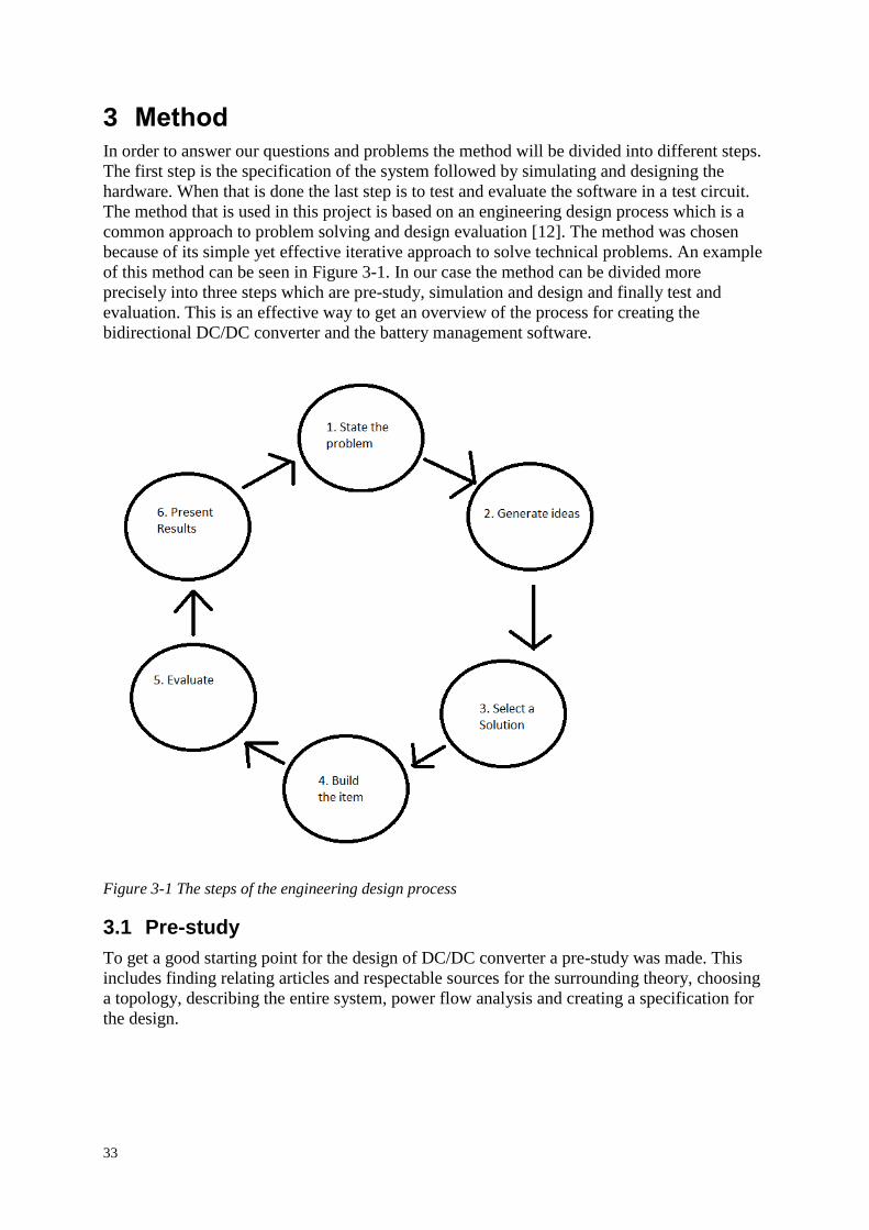
3 Method In order to answer our questions and problems the method will be divided into different steps.
The first step is the specification of the system followed by simulating and designing the
hardware. When that is done the last step is to test and evaluate the software in a test circuit.
The method that is used in this project is based on an engineering design process which is a
common approach to problem solving and design evaluation [12]. The method was chosen
because of its simple yet effective iterative approach to solve technical problems. An example
of this method can be seen in Figure 3-1. In our case the method can be divided more
precisely into three steps which are pre-study, simulation and design and finally test and
evaluation. This is an effective way to get an overview of the process for creating the
bidirectional DC/DC converter and the battery management software.
Figure 3-1 The steps of the engineering design process
3.1 Pre-study
To get a good starting point for the design of DC/DC converter a pre-study was made. This
includes finding relating articles and respectable sources for the surrounding theory, choosing
a topology, describing the entire system, power flow analysis and creating a specification for
the design.
34
3.1.1 System Overview
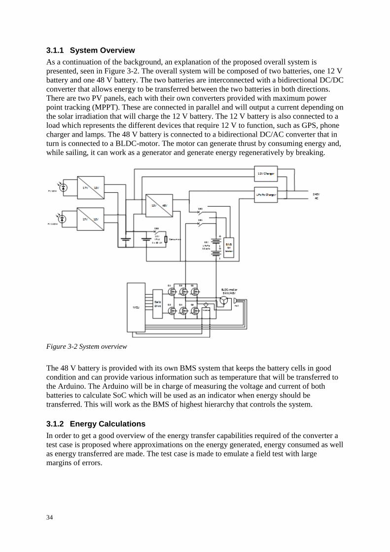
As a continuation of the background, an explanation of the proposed overall system is
presented, seen in Figure 3-2. The overall system will be composed of two batteries, one 12 V
battery and one 48 V battery. The two batteries are interconnected with a bidirectional DC/DC
converter that allows energy to be transferred between the two batteries in both directions.
There are two PV panels, each with their own converters provided with maximum power
point tracking (MPPT). These are connected in parallel and will output a current depending on
the solar irradiation that will charge the 12 V battery. The 12 V battery is also connected to a
load which represents the different devices that require 12 V to function, such as GPS, phone
charger and lamps. The 48 V battery is connected to a bidirectional DC/AC converter that in
turn is connected to a BLDC-motor. The motor can generate thrust by consuming energy and,
while sailing, it can work as a generator and generate energy regeneratively by breaking.
Figure 3-2 System overview
The 48 V battery is provided with its own BMS system that keeps the battery cells in good
condition and can provide various information such as temperature that will be transferred to
the Arduino. The Arduino will be in charge of measuring the voltage and current of both
batteries to calculate SoC which will be used as an indicator when energy should be
transferred. This will work as the BMS of highest hierarchy that controls the system.
3.1.2 Energy Calculations
In order to get a good overview of the energy transfer capabilities required of the converter a
test case is proposed where approximations on the energy generated, energy consumed as well
as energy transferred are made. The test case is made to emulate a field test with large
margins of errors.
35
3.1.2.1 Test Case
Table 3-1 shows a simplified version of the energy available and what output and input
energy is expected in the system using the values given for batteries and PV panels in the
appendix (8).
Table 3-1 Values from test case
Battery 12 V 48 V Total
Total capacity [Wh] 2765 2304 5069
Output energy
[Wh/day]
555 1333 1888
Input energy
[Wh/day]
552 300 852
The total capacity of the batteries is taken from their respective specifications and the
available energy for the respective batteries can be calculated using (2-47)
𝑊12 = 𝐶𝑛𝑜𝑚,12 ⋅ 𝐷𝑜𝐷𝑚𝑎𝑥,12 ⋅ 𝑈12,𝑛𝑜𝑚 = 384 ⋅ 0.6 ⋅ 12 ≈ 2765 Wh (3-1)
𝑊48 = 𝐶𝑛𝑜𝑚,48 ⋅ 𝐷𝑜𝐷𝑚𝑎𝑥,48 ⋅ 𝑈48,𝑛𝑜𝑚 = 60 ⋅ 0.75 ⋅ 48 ≈ 2304 Wh (3-2)
It should be noted that this energy is what is available without deep discharging. More energy
can be extracted at risk of decreasing the expected lifetime of the battery. The output energy
of the 12 V battery is approximated using normal values for the different electrical consumers
on the boat such as a refrigerator, GPS and lamps. The output energy of the 48 V battery is
calculated from one hour of driving at 5 knots with a battery to motor efficiency of 75%. The
input energy to the 12 V battery is approximated by assuming the PV panels get 3 hours of
1000W/m3 solar irradiance per day. The input to the 48 V battery which is from when the
generator mode is on during sailing, is approximated to be 150 W and turned on 2 hours a
day.
As can be seen in Table 3-1, without energy transfer the 48 V battery will run out in about 2
days and with lossless energy transfer both batteries will run out in about 5 days in this test
case.
3.1.2.2 Energy Transfer
Since losses are prevalent in a converter it is a good idea to try to limit the amount of power
that needs to be converted. Optimally the converter does not need to be used and only the
power generated from the generator and solar panels is consumed by their own respective
circuits. But in most cases including our test case the energy consumed exceeds the generated
amount, a strategy for energy transfer needs to be made to minimize losses. Designing an
optimal strategy for efficiency is however not possible since, unlike our test case, the energy
consumed and generated is unpredictable and varies. In the scope of this project a simpler
strategy will be proposed due to limitations. This strategy aims to equalize the charge of the
batteries so that the batteries of each circuit can store the power that is generated in each
36
respective circuit. It will accomplish this by transferring energy quickly if the difference in
each batteries state of charge is large and slowly if the difference is small. It will stop
transferring when the difference in SoC of the batteries are similar. An initial strategy for
these transferring limits can be seen in Figure 3-3.
Figure 3-3 Proposed charge schedule where the SoC for the 48 V battery is on the Y-axis and the SoC
for the 12 V battery is on the X-axis
3.1.3 Comparison of Bidirectional Buck-Boost
The two batteries in the system will work together using a bidirectional buck-boost converter.
This opens the possibility to charge and discharge both batteries which is needed to optimize
the power flow. To decide the design of the dc/dc converter a comparison between different
topologies and solutions are needed.
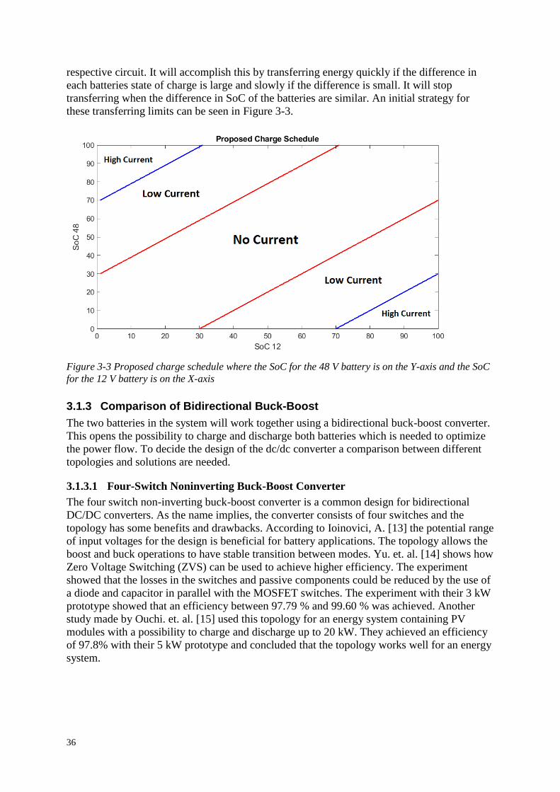
3.1.3.1 Four-Switch Noninverting Buck-Boost Converter
The four switch non-inverting buck-boost converter is a common design for bidirectional
DC/DC converters. As the name implies, the converter consists of four switches and the
topology has some benefits and drawbacks. According to Ioinovici, A. [13] the potential range
of input voltages for the design is beneficial for battery applications. The topology allows the
boost and buck operations to have stable transition between modes. Yu. et. al. [14] shows how
Zero Voltage Switching (ZVS) can be used to achieve higher efficiency. The experiment
showed that the losses in the switches and passive components could be reduced by the use of
a diode and capacitor in parallel with the MOSFET switches. The experiment with their 3 kW
prototype showed that an efficiency between 97.79 % and 99.60 % was achieved. Another
study made by Ouchi. et. al. [15] used this topology for an energy system containing PV
modules with a possibility to charge and discharge up to 20 kW. They achieved an efficiency
of 97.8% with their 5 kW prototype and concluded that the topology works well for an energy
system.
37
Figure 3-4 Four-Switch Noninverting Buck-Boost Converter circuit
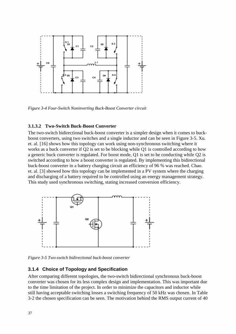
3.1.3.2 Two-Switch Buck-Boost Converter
The two-switch bidirectional buck-boost converter is a simpler design when it comes to buck-
boost converters, using two switches and a single inductor and can be seen in Figure 3-5. Xu.
et. al. [16] shows how this topology can work using non-synchronous switching where it
works as a buck converter if Q2 is set to be blocking while Q1 is controlled according to how
a generic buck converter is regulated. For boost mode, Q1 is set to be conducting while Q2 is
switched according to how a boost converter is regulated. By implementing this bidirectional
buck-boost converter in a battery charging circuit an efficiency of 96 % was reached. Chao.
et. al. [3] showed how this topology can be implemented in a PV system where the charging
and discharging of a battery required to be controlled using an energy management strategy.
This study used synchronous switching, stating increased conversion efficiency.
Figure 3-5 Two-switch bidirectional buck-boost converter
3.1.4 Choice of Topology and Specification
After comparing different topologies, the two-switch bidirectional synchronous buck-boost
converter was chosen for its less complex design and implementation. This was important due
to the time limitation of the project. In order to minimize the capacitors and inductor while
still having acceptable switching losses a switching frequency of 50 kHz was chosen. In Table
3-2 the chosen specification can be seen. The motivation behind the RMS output current of 40
38
A was due to the possibility of charging the 12 V battery with at least 10% of the capacity
being 38.4 A. The current ripple for charging the battery be specified to maximum 15% since
a larger current ripple may affect the battery lifespan.
Table 3-2 Specification for the system
Specification
Input voltage 48 V Output voltage 12 V
RMS input current 10 A RMS output current 40 A
Rated power 480 W Output current ripple 15%
Switching frequency PWM 50 kHz ILmax 46 A
Max MOSFET voltage peak
VDS 120 V
3.2 Simulation
The simulations of the system were divided into two parts, overall simulation of the topology
in MATLAB Simulink. More detailed simulation of components and driver stage in
MultiSIM. The reason for this is that Simulink have more detailed models of batteries while
MultiSIM has better possibilities of simulating non-ideal components. Simulink also has
support for Arduino which is very useful when developing the software for later.
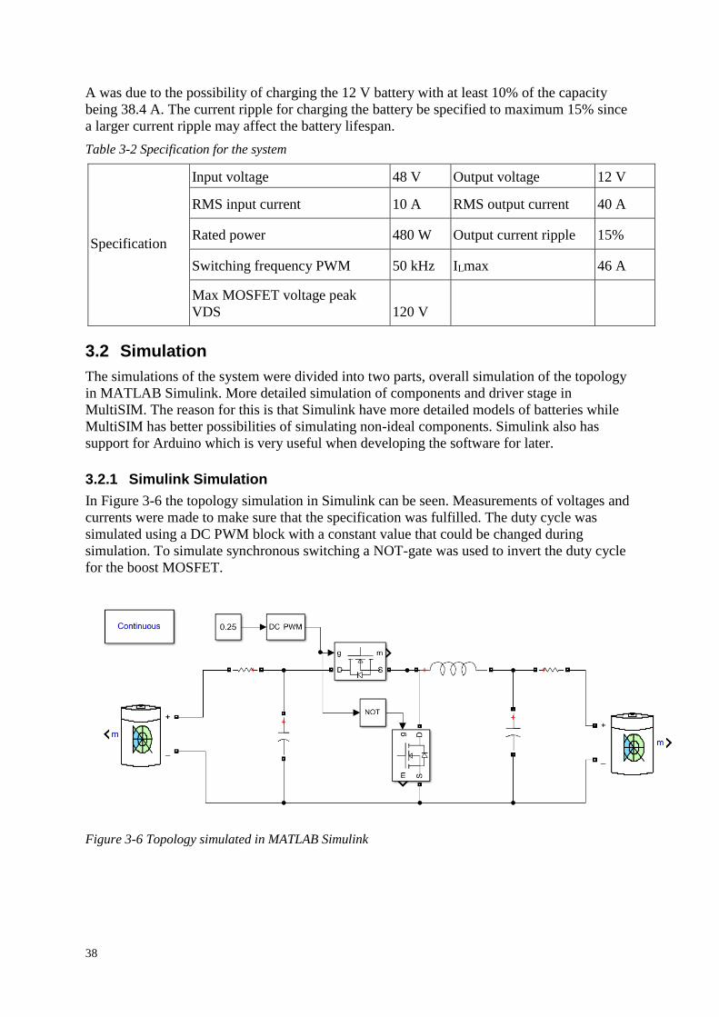
3.2.1 Simulink Simulation
In Figure 3-6 the topology simulation in Simulink can be seen. Measurements of voltages and
currents were made to make sure that the specification was fulfilled. The duty cycle was
simulated using a DC PWM block with a constant value that could be changed during
simulation. To simulate synchronous switching a NOT-gate was used to invert the duty cycle
for the boost MOSFET.
Figure 3-6 Topology simulated in MATLAB Simulink

39
3.2.2 Multisim Simulation
To ensure the specification for the chosen MOSFET IPB044N15N5 simulations of the
switching characteristics were made in MultiSIM. To simulate the potential overvoltage from
parasitic inductances discussed in 2.2.1 that occurs when the upper MOSFET switches, the
circuit in Figure 3-7 was used. Different values for components were used to make sure the
specification was met. The constant current source represents the current in the inductor. To
represent the DC bus connected to the 48 V battery, the capacitors of 75 µF and 400 µF with
their parasitic inductances of 1 nH and 6 nH are used. This method was used to decide the
values of the external resistances Rgon and Rgoff.
To provide more exact simulations the models for the driver circuit and the MOSFET that
were used are provided by the manufacturers. As these models are made by the manufacturers
they contain more trustworthy parameters and characteristics to emulate the component.
Figure 3-7 MOSFET simulation test circuit without component values in MultiSIM
3.3 Components and Design
All components need to be chosen so that the specifications are met. A certain safety margin
is added to ensure that components do not break even when exceeding specification if for
example an error in the system occur.
3.3.1 MOSFET
When selecting a power MOSFET for the DC/DC the most crucial parameters are the high
voltage and current. Due to availability for early testing and being sufficient for the
application the MOSFET IPB044N15N5 from Infineon was selected [17]. With the
parameters of 150 V VDS and 174 A ID it is probably overkill for this application and was
selected because of familiarity and coincidences.
3.3.2 Driver Circuit
To be able to turn the MOSFETs at a switch frequency of 50 kHz a driver circuit is needed.
The chosen driver circuit is the integrated circuit UCC5390SC. The IC is a suitable candidate
due to the high output voltage to minimize losses in the MOSFET but also the high sink and
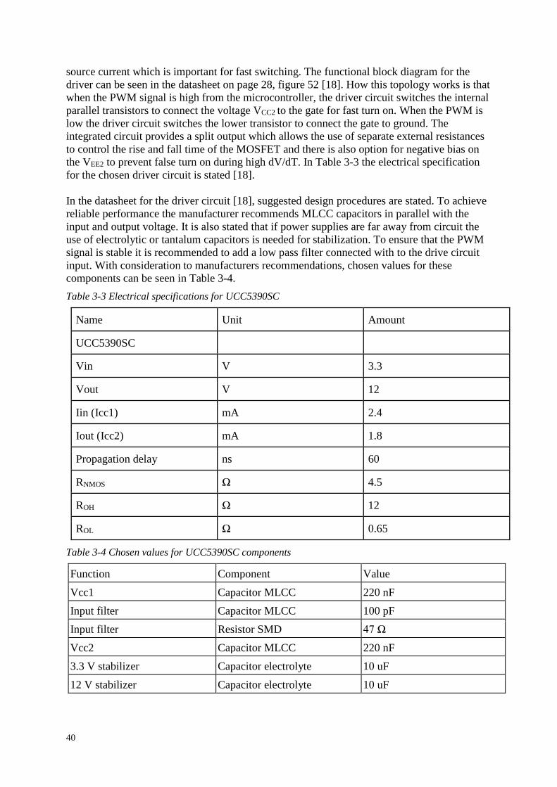
40
source current which is important for fast switching. The functional block diagram for the
driver can be seen in the datasheet on page 28, figure 52 [18]. How this topology works is that
when the PWM signal is high from the microcontroller, the driver circuit switches the internal
parallel transistors to connect the voltage VCC2 to the gate for fast turn on. When the PWM is
low the driver circuit switches the lower transistor to connect the gate to ground. The
integrated circuit provides a split output which allows the use of separate external resistances
to control the rise and fall time of the MOSFET and there is also option for negative bias on
the VEE2 to prevent false turn on during high dV/dT. In Table 3-3 the electrical specification
for the chosen driver circuit is stated [18].
In the datasheet for the driver circuit [18], suggested design procedures are stated. To achieve
reliable performance the manufacturer recommends MLCC capacitors in parallel with the
input and output voltage. It is also stated that if power supplies are far away from circuit the
use of electrolytic or tantalum capacitors is needed for stabilization. To ensure that the PWM
signal is stable it is recommended to add a low pass filter connected with to the drive circuit
input. With consideration to manufacturers recommendations, chosen values for these
components can be seen in Table 3-4.
Table 3-3 Electrical specifications for UCC5390SC
Name Unit Amount
UCC5390SC
Vin V 3.3
Vout V 12
Iin (Icc1) mA 2.4
Iout (Icc2) mA 1.8
Propagation delay ns 60
RNMOS Ω 4.5
ROH Ω 12
ROL Ω 0.65
Table 3-4 Chosen values for UCC5390SC components
Function Component Value
Vcc1 Capacitor MLCC 220 nF
Input filter Capacitor MLCC 100 pF
Input filter Resistor SMD 47 Ω
Vcc2 Capacitor MLCC 220 nF
3.3 V stabilizer Capacitor electrolyte 10 uF
12 V stabilizer Capacitor electrolyte 10 uF

41
3.3.3 ˗5 V Converter
In the datasheet for the gate driver UCC5390SC it is stated that there is a function for
undervoltage lockout to prevent the voltage from being too low [18]. Since the 12 V battery
has a VMIN of 10.4 V a ˗5 V converter is needed to prevent this behavior. The chosen
converter is the integrated circuit LT1054 from Texas Instruments and it was chosen due to
availability from another project and being sufficient for the application [19].
The output of the ˗5 V converter will be connected to the VEE2 pin of the gate driver and this
will affect the switching properties. By having negative bias, the voltage will rise from ˗5 V to
12 V when switching instead of 0 V to 12 V which leads to somewhat longer turn-on delay,
but rise times are same. However, it also provides a safety margin for accidental turn on. To
make sure the IC works correctly the manufacturer provides recommendations in the
datasheet for design considerations. Following the design suggestions, the component values
in Table 3-5 were chosen [19].
Table 3-5 Chosen values for LT1054 circuit components
Name Component Value
Cin Capacitor tantalum 10 uF
C1 Capacitor MLCC 2.2 nF
R1 Resistor SMD 22 kΩ
R2 Resistor SMD 120 kΩ
Cout1 Capacitor MLCC 1 uF
Cout2 Capacitor tantalum 10 uF
3.3.4 Bootstrap
Since the upper transistor is not connected to ground it needs a bootstrap circuit to have a
floating ground. The bootstrap circuit contains of a resistor, capacitor and a diode. The design
of the bootstrap capacitor was based on the suggestions by Allegro in their datasheet for a
MOSFET controller [20]. They stated that the bootstrap capacitor should neither be too big or
too small to prevent wasting time. By using a reasonable factor of 20 times higher charge the
formula for the bootstrap capacitor is
𝐶𝐵𝑂𝑂𝑇 =
𝑄𝐺𝐴𝑇𝐸 ⋅ 20
𝑉𝐵𝑂𝑂𝑇=
100 ⋅ 10−9 ⋅ 20
12= 167 nF
(3-3)
Where the QGATE is the gate charge of the MOSFET and the VBOOT is the 12 V connected from
the battery. A capacitor of 220 nF was chosen to have some margin.
When designing the bootstrap resistor, it is important for it to have a small resistance to
shorten the time of charging the capacitor. The resistor therefore also needs to withstand large
energy pulses during short periods of time. The thick film resistor RCL12181R00FKEK by
Vishay of 1 Ω was chosen since it can withstand continuous pulses of over 100 W for 1 µs
[21].

42
The proposed bootstrap diode is the CDBC5150-HF from Comchip Technology which was
decided due to high efficiency, fast switching and a reverse voltage of 150 V [22]. This is
important to withstand potential voltage spikes. It also has low forward voltage and can
withstand the pulse of high current when charging the bootstrap capacitor.
3.3.5 Inductor
The design choices for the inductor in the DC/DC converter are limited by frequency and high
current. The inductor should be able to operate at 40 A with a switching frequency of 50 kHz.
According to [5] ferrite is a good choice at frequencies higher than 10 kHz due to small eddy
current losses. The specification stated that the output ripple current should not exceed 15% of
Iout which means that the inductor should not produce a larger ripple than 6 A. Following the
suggested design calculations from Texas Instruments [7] using equation (2-34)
𝐿 >
𝑉𝑜𝑢𝑡 ⋅ (𝑉𝑖𝑛𝑚𝑎𝑥 − 𝑉𝑜𝑢𝑡)
𝐾𝑖𝑛𝑑 ⋅ 𝐹𝑠𝑤 ⋅ 𝑉𝑖𝑛𝑚𝑎𝑥 ⋅ 𝐼𝑜𝑢𝑡=
12 ⋅ (60.8 − 12)
0.15 ⋅ 50000 ⋅ 60.8 ⋅ 40= 32μH (3-4)
where Vinmax is 60.8 V, Vout is 12 V, Iout is 40 A ,Fsw is 50 kHz and Kind is 0.15 as in the 15%
current ripple. For boost mode equation (2-35) is used
𝐿 >
𝑉𝑖𝑛𝑚𝑖𝑛2 ⋅ (𝑉𝑜𝑢𝑡 − 𝑉𝑖𝑛𝑚𝑖𝑛)
𝐾𝑖𝑛𝑑 ⋅ 𝐹𝑠𝑤 ⋅ 𝐼𝑜𝑢𝑡 ⋅ 𝑉𝑜𝑢𝑡2=
122 ⋅ (48 − 12)
0.15 ⋅ 50000 ⋅ 10 ⋅ 482= 30 μH
(3-5)
where Vinmin for boost is 12 V, Vout is 48 V and Iout is 10 A. This results in the inductor
needing to have a value of at least 32 µH for this application.
An inductor that suited this specification was unfortunately not available at the suppliers and
therefore it was decided to buy a magnetic core and wind the copper wire by hand. A ferrite
core of the material N27 was proposed due to its optimal frequency at minimum 25 kHz and
maximum 150 kHz while also being available at the suppliers [23]. In Table 3-6 the
dimensions from the selected inductor datasheet is shown [23]. By using equations from
chapter 2.3.1 the calculated values in Table 3-6 are stated. The limitation was that the
magnetic flux density should not exceed 320 mT to keep the permeability µr larger than 1500
H/m. The chosen core has an air gap of 2.6 mm which will also limit the magnetic flux
density given equation (2-36) which results in a limitation to the magnetic flux, using
equation (2-37)
𝛷 =
𝐵
𝐴𝑒=
320
570 ⋅ 109= 182 μWb (3-6)
which limits the amount of turns by a maximum using equation (2-38)
𝑁 =
𝛷 ⋅ 𝑅𝑡𝑜𝑡
𝐼=
182 ⋅ 10−6 ⋅ 3390729
50= 12.34 turns (3-7)
where the current is set to 50 A as a safety measure. With the decided amount of turns to be
12 the inductor value of L is calculated by equation (2-39)
𝐿 =
𝑁2
𝑅𝑡𝑜𝑡=
122
3390729 ≈ 42 μH (3-8)
which fulfilled the condition of being larger than 32 µH.

43
The design of the conductor was with consideration to high current which in to have a large
amount of Litz threads to increase decrease the power losses. The total cross section area of
the copper wire 𝐴𝑐𝑢 was decided to be larger than 5.3 mm2 to limit the power losses and to
handle the specified current of 40 A. The used Litz strand had a diameter of 0.25 mm leading
to the strand area being
𝐴𝑧 =𝜋
4⋅ 0.252 ≈ 0.05 mm2
(3-9)
where the use of 120 Litz strands is used to satisfy an area larger than 5.3 mm2 with some
safety margin. With 120 Litz strands the total cross section area of the copper wire is
𝐴𝑐𝑢 = 𝐴𝑧 ⋅ 𝑧 = 0.05 ⋅ 120 = 5.89 mm2 (3-10)
by using equation (2-41). Which concludes in the current density
𝐽𝑟𝑚𝑠 =
𝐼𝑅𝑀𝑆
𝐴𝐶𝑈=
40
5.89= 6.79 A/mm2
(3-11)
by using the current RMS of 40 A from the specification. The selected inductor and proposed
conductor the resulting fill factor is calculated as
𝑘𝑐𝑢 =
𝑁 ⋅ 𝐴𝑐𝑢
𝐴𝑤=
12 ⋅ 5.89
385.77= 0.18
(3-12)
where the cross-sectional area for the conductor is given by
𝐴𝑤 = 𝑊𝑤 ⋅ (𝐷𝑡 − 𝐷𝑒) = 16.7 ⋅ (48.8 − 25.7) = 385.77 mm2 (3-13)
where the dimensions Ww, Dt and De are given in the datasheet, seen in Table 3-6
Table 3-6 Dimensions and calculations for selected inductor ferrite core
Dimensions
Ie 109 mm
Calculated
N 12 turns
Ae 570 mm2 Ag 629 mm2
Ve 62000 mm3 Rcore 101450 H-1
De 25.7 mm Rgap 3289279 H-1
Dt 48.8 mm Rtot 3390729 H-1
Wc 62 mm 𝛷 1.8E-04 Wb
g 2.6 mm B 310.4 mT
Ww 16.7 mm L 42.47 mH
Wt 24.5 mm

44
3.3.6 Power Losses
The DC/DC converter will have the majority of the power losses in the inductor as well as the
MOSFETs. The power losses are divided into two sections for the components, core and
winding losses for the inductor, switching and conduction for the MOSFET. Some additional
power losses will appear in the ˗5 V converter and in the driver stage. To prepare the needed
heatsink the power losses are calculations after worst case.
With the chosen MOSFET we get the following conduction power losses
𝑃𝑜𝑛−𝑏𝑜𝑜𝑠𝑡 = 𝑟𝑜𝑛𝐼𝑜𝑛
2𝑡𝑜𝑛
𝑇𝑠= 4.4 ⋅ 10−3 ⋅ 402 ⋅ 0.75 = 5.28 W
(3-14)
for the boost MOSFET with a duty cycle of 75% and the following for the buck MOSFET
𝑃𝑜𝑛−𝑏𝑢𝑐𝑘 = 𝑟𝑜𝑛𝐼𝑜𝑛
2𝑡𝑜𝑛
𝑇𝑠= 4.4 ⋅ 10−3 ⋅ 402 ⋅ 0.25 = 1.76 W (3-15)
with a duty cycle of 25%. These calculations are for worst case situation when conducting 40
A. The switching with a switching frequency of 50 kHz the power losses are calculated using
equation (2-28)
𝑃𝑠 = 0.5 ⋅ 48 ⋅ 10 ⋅ 50000 ⋅ (210 ns + 141ns + 17ns + 112ns) = 5.77 W
(3-16)
where the values for Vd and Io are considered to be from the 48 V battery. The switching times
are calculated with the maximum values from MOSFET datasheet [17] and with consideration
to the chosen driver circuit resistances and the external gate resistances. With the chosen
external resistances of Rextoff of 5.6 Ω and Rexton of 33 Ω the total gate resistance is
𝑅𝑔𝑜𝑛 = 𝑅𝑒𝑥𝑡𝑜𝑛 + 𝑅𝑁𝑀𝑂𝑆||𝑅𝑂𝐻 = 33 +
12 ⋅ 4.5
12 + 4.5= 36.2727 Ω (3-17)
𝑅𝑔𝑜𝑓𝑓 = 𝑅𝑒𝑥𝑡𝑜𝑓𝑓 + 𝑅𝑂𝐿 = 5.6 + 0.65 = 6.25 Ω. (3-18)
The total power losses from the MOSFETs concludes in
𝑃𝑀𝑂𝑆𝐹𝐸𝑇 = 𝑃𝑜𝑛−𝑏𝑜𝑜𝑠𝑡 + 𝑃𝑜𝑛−𝑏𝑢𝑐𝑘 + 2 ⋅ 𝑃𝑠𝑤 = 5.28 + 1.76 + 2 ⋅ 5.77 = 18.58 W
(3-19)
where the switching losses are assumed to be the same for both MOSFETs.
The other big contributor of power losses is the inductor, the winding losses produced by the
chosen inductor is calculated to be
𝑃𝑤 = 𝜌 ⋅ 𝑘𝑐𝑢 ⋅ 𝐽𝑟𝑚𝑠2 ⋅ 𝑉𝑤 = 22 ⋅ 10−9 ⋅ 0.18 ⋅ 6.792 ⋅ 45144 ⋅ 1000 = 8.4 W
(3-20)
where the used IRMS is set to be 40 A and 𝜌is the resistivity of copper at 100. Since the core
losses in the inductor are dependent on the material, the datasheet for N27 by TDK was used
[23] in the third graph on page 5 the relative core losses versus frequency relationship is
shown. By calculating the magnetic flux density
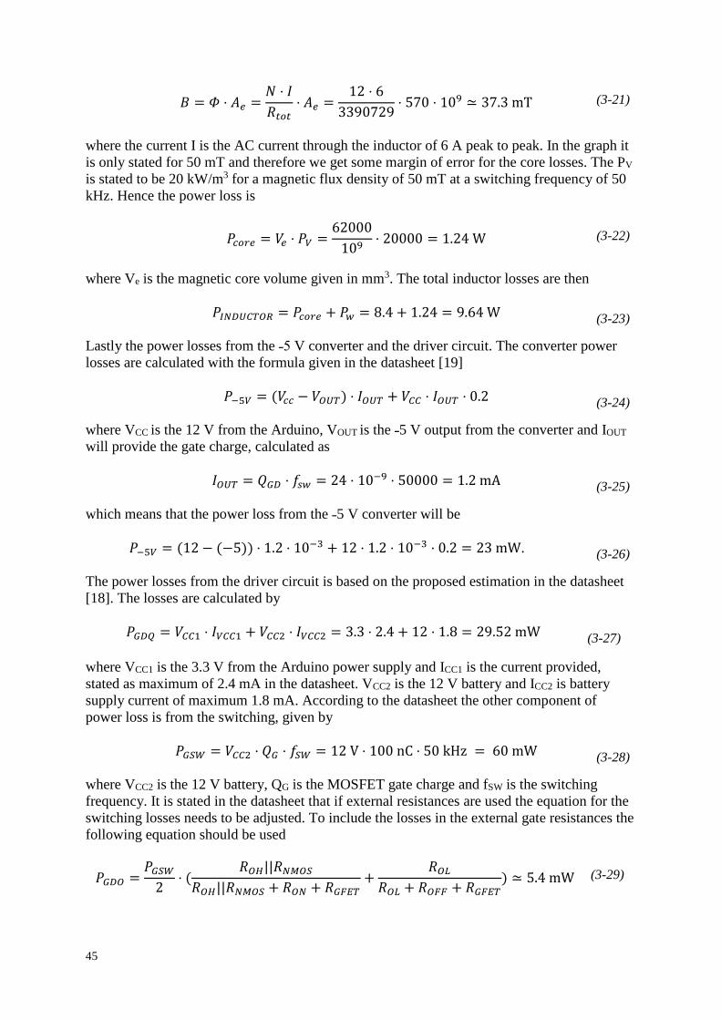
45
𝐵 = 𝛷 ⋅ 𝐴𝑒 =
𝑁 ⋅ 𝐼
𝑅𝑡𝑜𝑡⋅ 𝐴𝑒 =
12 ⋅ 6
3390729⋅ 570 ⋅ 109 ≃ 37.3 mT
(3-21)
where the current I is the AC current through the inductor of 6 A peak to peak. In the graph it
is only stated for 50 mT and therefore we get some margin of error for the core losses. The PV
is stated to be 20 kW/m3 for a magnetic flux density of 50 mT at a switching frequency of 50
kHz. Hence the power loss is
𝑃𝑐𝑜𝑟𝑒 = 𝑉𝑒 ⋅ 𝑃𝑉 =
62000
109⋅ 20000 = 1.24 W
(3-22)
where Ve is the magnetic core volume given in mm3. The total inductor losses are then
𝑃𝐼𝑁𝐷𝑈𝐶𝑇𝑂𝑅 = 𝑃𝑐𝑜𝑟𝑒 + 𝑃𝑤 = 8.4 + 1.24 = 9.64 W
(3-23)
Lastly the power losses from the ˗5 V converter and the driver circuit. The converter power
losses are calculated with the formula given in the datasheet [19]
𝑃−5𝑉 = (𝑉𝑐𝑐 − 𝑉𝑂𝑈𝑇) ⋅ 𝐼𝑂𝑈𝑇 + 𝑉𝐶𝐶 ⋅ 𝐼𝑂𝑈𝑇 ⋅ 0.2
(3-24)
where VCC is the 12 V from the Arduino, VOUT is the ˗5 V output from the converter and IOUT
will provide the gate charge, calculated as
𝐼𝑂𝑈𝑇 = 𝑄𝐺𝐷 ⋅ 𝑓𝑠𝑤 = 24 ⋅ 10−9 ⋅ 50000 = 1.2 mA
(3-25)
which means that the power loss from the ˗5 V converter will be
𝑃−5𝑉 = (12 − (−5)) ⋅ 1.2 ⋅ 10−3 + 12 ⋅ 1.2 ⋅ 10−3 ⋅ 0.2 = 23 mW.
(3-26)
The power losses from the driver circuit is based on the proposed estimation in the datasheet
[18]. The losses are calculated by
𝑃𝐺𝐷𝑄 = 𝑉𝐶𝐶1 ⋅ 𝐼𝑉𝐶𝐶1 + 𝑉𝐶𝐶2 ⋅ 𝐼𝑉𝐶𝐶2 = 3.3 ⋅ 2.4 + 12 ⋅ 1.8 = 29.52 mW
(3-27)
where VCC1 is the 3.3 V from the Arduino power supply and ICC1 is the current provided,
stated as maximum of 2.4 mA in the datasheet. VCC2 is the 12 V battery and ICC2 is battery
supply current of maximum 1.8 mA. According to the datasheet the other component of
power loss is from the switching, given by
𝑃𝐺𝑆𝑊 = 𝑉𝐶𝐶2 ⋅ 𝑄𝐺 ⋅ 𝑓𝑆𝑊 = 12 V ⋅ 100 nC ⋅ 50 kHz = 60 mW
(3-28)
where VCC2 is the 12 V battery, QG is the MOSFET gate charge and fSW is the switching
frequency. It is stated in the datasheet that if external resistances are used the equation for the
switching losses needs to be adjusted. To include the losses in the external gate resistances the
following equation should be used
𝑃𝐺𝐷𝑂 =𝑃𝐺𝑆𝑊
2⋅ (
𝑅𝑂𝐻||𝑅𝑁𝑀𝑂𝑆
𝑅𝑂𝐻||𝑅𝑁𝑀𝑂𝑆 + 𝑅𝑂𝑁 + 𝑅𝐺𝐹𝐸𝑇+
𝑅𝑂𝐿
𝑅𝑂𝐿 + 𝑅𝑂𝐹𝐹 + 𝑅𝐺𝐹𝐸𝑇) ≃ 5.4 mW
(3-29)
46
where the values for ROH, ROL, and RNMOS are stated in Table 3-4 for the driver circuit and
RON, ROFF are the external gate resistance of 33 Ω and 5.6 Ω. The value for RGFET is the
typical gate resistance of 0.8 Ω from MOSFET datasheet. The total power loss for the driver
is then
𝑃𝐷𝑅𝐼𝑉𝐸𝑅 = 𝑃𝐺𝐷𝑄 + 𝑃𝐺𝐷𝑂 = 29.52 mW + 5.4 mW ≃ 35 mW
(3-30)
giving us the total power losses in the system to be
𝑃𝑙𝑜𝑠𝑠−𝑡𝑜𝑡𝑎𝑙 = 𝑃𝑀𝑂𝑆𝐹𝐸𝑇 + 𝑃𝐼𝑁𝐷𝑈𝐶𝑇𝑂𝑅 + 𝑃−5𝑉 + 𝑃𝐷𝑅𝐼𝑉𝐸𝑅
= 18.58 + 9.64 + 0.023 + 2 ⋅ 0.035 = 28.313 W
(3-31)
which indicates that the circuit will generate a lot of heat. This calculation will be used as a
basis when designing the heat sink for the system.
3.3.7 Thermal Considerations
In order to understand the heat flow in the power electronic circuit a heat flow diagram can be
seen in Figure 3-8. An equivalent circuit representing the heat flow from the switches to the
ambient air can be seen in Figure 3-9. During the project it was decided that the inductor is
placed outside the PCB and therefore is not included in the calculations.
Figure 3-8 Heat flow diagram
Figure 3-9 Equivalent heat flow circuit

47
To calculate a suitable heatsink for this system a desired value of the maximum junction
temperature Tj,max is chosen to 80 and ambient temperature Ta 30 , which gives a case
temperature of 72.5 , which is acceptable. The power dissipated is approximated from the
calculated values with an added safety margin where the total power dissipated from the
MOSFETs, Ptot, is chosen to 20 W. In order to calculate the worst case maximum junction
temperature, the maximum power dissipated from a single MOSFET PQmax is assumed to be
15 W. The junction to case thermal resistivity Rth jc can be found in the MOSFETs datasheet
and is 0.5 W/°K. The case to heatsink thermal resistivity is
𝑅𝑡ℎ 𝑐𝑠 = 𝑅𝑡ℎ 𝑓𝑜𝑖𝑙 + 𝑅𝑡ℎ 𝑝𝑎𝑑 = 0.12 + 0.47 = 0.59 W/°K
(3-32)
where Rth foil is the thermal resistivity of the isolating thermal foil which lies pressed between
the heatsink and the vias on the opposite side of the MOSFETs on the PCB. Rth pad is the
thermal resistivity of the vias that the MOSFETs are placed on and is calculated using the
online PCB via calculator [24].
Using the formula (2-46) the maximum thermal resistivity of the heatsink, Rth sa, can be
calculated as
𝑅𝑡ℎ 𝑠𝑎 =
〖(𝑇〗𝑠 − 𝑇𝑎)
𝑃𝑡𝑜𝑡=
𝑇𝑐,𝑚𝑎𝑥 − (𝑅𝑡ℎ 𝑐𝑠 ∗ 𝑃𝑄 𝑚𝑎𝑥) − 𝑇𝑎
𝑃𝑡𝑜𝑡
=(𝑇𝑗,𝑚𝑎𝑥 − (𝑅𝑡ℎ 𝑗𝑐 ∗ 𝑃𝑄 𝑚𝑎𝑥)) − (𝑅𝑡ℎ 𝑐𝑠 ∗ 𝑃𝑄 𝑚𝑎𝑥) − 𝑇𝑎
𝑃𝑡𝑜𝑡
(3-33)
𝑅𝑡ℎ 𝑠𝑎 = ((80 − (0.5 ∗ 15)) − (0.59 ∗ 15) − 80)/20 = 1.6825 W/°K.
Choosing a heatsink with a thermal resistivity Rth sa of 1.5 W/°K the maximum junction
temperature Tj,max can be calculated as
𝑇𝑗,𝑚𝑎𝑥 = 𝑇𝑐,𝑚𝑎𝑥 + (𝑅𝑡ℎ 𝑗𝑐 ∗ 𝑃𝑄 𝑚𝑎𝑥) = 𝑇𝑠 + (𝑅𝑡ℎ 𝑐𝑠 ∗ 𝑃𝑄 𝑚𝑎𝑥) + (𝑅𝑡ℎ 𝑗𝑐 ∗ 𝑃𝑄 𝑚𝑎𝑥)
𝑇𝑗,𝑚𝑎𝑥 = 𝑇𝑎 + (𝑅𝑡ℎ 𝑠𝑎 + 𝑃𝑡𝑜𝑡) + (𝑅𝑡ℎ 𝑐𝑠 ∗ 𝑃𝑄 𝑚𝑎𝑥) + (𝑅𝑡ℎ 𝑗𝑐 ∗ 𝑃𝑄 𝑚𝑎𝑥)
𝑇𝑗,𝑚𝑎𝑥 = 30 + (1.5 + 20) + (0.59 ∗ 15) + (0.5 ∗ 15) = 76.35 .
(3-34)

48
3.3.8 PCB Design
A design of the PCB was made using Ultiboard. Figure 3-10 shows an image of the complete
control system, where the leftmost part (in blue square) is contains the footprints and traces
for the components needed for the bidirectional DC/DC converter that is the focus in this
report. The rightmost part (in grey square) contains footprints and traces for the components
for the inverter needed to drive the BLDC motor from the 48 V battery.
Figure 3-10 PCB design for DC/DC converter (in blue square) and BLDC inverter (in grey square)
When placing the components footprints on the board it is important to consider the thermal
design. Since a surface mounted power transistor is to be used, the through-hole components
must be placed on the edges of the PCB to provide adequate room for the heatsink to be
mounted below the power transistors as the heatsink is pressed against a thermal pad that lies
on a matrix of vias that will conduct the heat from the transistor to the heatsink. This also
requires that all other components that should be placed close to the transistors are surface
mounted devices as well to isolate them from the heatsink.
It is also important to consider how stray inductances from the traces needed to connect
components will affect components. Picking components that are surface mounted and
placing them close together can help minimize these inductances. Traces that will have a large
current flowing through them need to be made wider to reduce resistance and thus losses.
Figure 3-11 shows a closeup of the PCB design for the DC/DC converter where the width of
the traces are calculated using the trace width calculator [25] that recommended 45 mm width
for 40 A traces and 10 mm for 10 A traces.

49
Figure 3-11 Closeup of PCB design for DC/DC converter (left of blue line)
3.4 Microcontroller and Software
The microcontroller in the system that will control the PWM, partial integrator (PI) regulator,
the battery management system and the BLDC motor is an Arduino Due. It contains of an
Atmel SAM3X8E ARM Cortex-M3 32-bit CPU and 54 digital inputs/output pins of which 12
can be used as PWM outputs. It also contains 12 analog inputs and 4 UARTs (Universal
Asynchronous Receiver-Transmitter). The maximum clock speed is 84 MHz and there is 512
Kb flash and 100 Kb SRAM [26].
The system requires multiple signals in order to work properly. The duty cycle for the
MOSFETs on the converter needs to be controlled to transfer the desired power. The
temperature needs to be observed to not break components. The voltage and current of each
battery needs to be measured to verify that they are at proper levels, if not, regulate them with
the PI regulator. By measuring the voltage and current the SoC will be calculated using
coulomb counting to decide the mode of operation [9].
3.4.1 Inputs
For the software to operate it will need different input signals from the circuit in order to
produce control signals. The signals from the circuit are: inductor current to the 12 V battery,
total current to the 12 V battery, including the current provided by the PV panels, voltage
measurement of the 12 V battery, ambient temperature measurement, a UART signal from the
48 V battery BMS, voltage and current to the 48 V battery be received.

50
3.4.2 Outputs
From the input signals the output, or control signals will be calculated. The output signals are
the PWM signals whose duty cycle will determine when the MOSFETs shall switch to their
conducting or blocking modes. Using the Arduinos built in PWM function a 50 kHz 10-bit
PWM is realized. The duty cycle will be regulated by a PI controller that requires a reference
value and a desired value. Depending on the batteries SoC the different charge or discharge
modes will be decided. The choosing of the operation modes are the same as the discussed in
the theory for the battery management system.
3.5 Software Test
To test the software before connecting it to the real system a test-bench was made. In Table
3-7 a list can be seen consisting of the components used for testing the software. The circuit
was configured as the chosen circuit topology to test both buck and boost operation with
voltage and current controlled PI. This was important to make sure that regulator was fast
enough before connecting two batteries together. By using both current and voltage regulated
PI the functions constant current and constant voltage charge discussed in 2.7 could be tested.
The software seen in Figure 3-12 was made in Simulink where interactive simulation was
used in combination with the Arduino Due to test the system. The software contains of two
Arduino inputs that provides the current and voltage measurements, the subsheets called PI
voltage and PI current contains discrete PI regulators with chosen constants for amplifying the
error. The subsheet called PWM contains a S-Function that configures the Arduino for 50 kHz
PWM and chosen duty cycle.
Table 3-7 Components used during software test
Microcontroller Arduino Due
Lead battery 12 V
Effect resistor 15 Ω
MOSFET IRFP4468PbF
˗5 V converter LT1054
Driver circuit UCC5390SC
Created inductor 42 µH
Current sensor LTS 25-NP
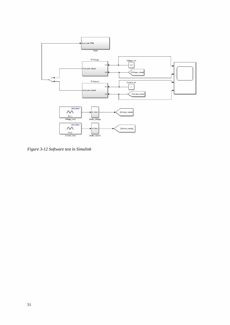
51
Figure 3-12 Software test in Simulink
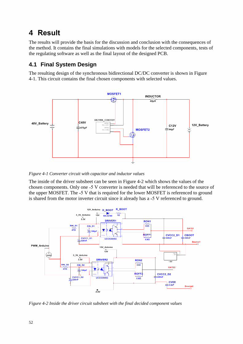
52
4 Result The results will provide the basis for the discussion and conclusion with the consequences of
the method. It contains the final simulations with models for the selected components, tests of
the regulating software as well as the final layout of the designed PCB.
4.1 Final System Design
The resulting design of the synchronous bidirectional DC/DC converter is shown in Figure
4-1. This circuit contains the final chosen components with selected values.
Figure 4-1 Converter circuit with capacitor and inductor values
The inside of the driver subsheet can be seen in Figure 4-2 which shows the values of the
chosen components. Only one ˗5 V converter is needed that will be referenced to the source of
the upper MOSFET. The ˗5 V that is required for the lower MOSFET is referenced to ground
is shared from the motor inverter circuit since it already has a ˗5 V referenced to ground.
Figure 4-2 Inside the driver circuit subsheet with the final decided component values
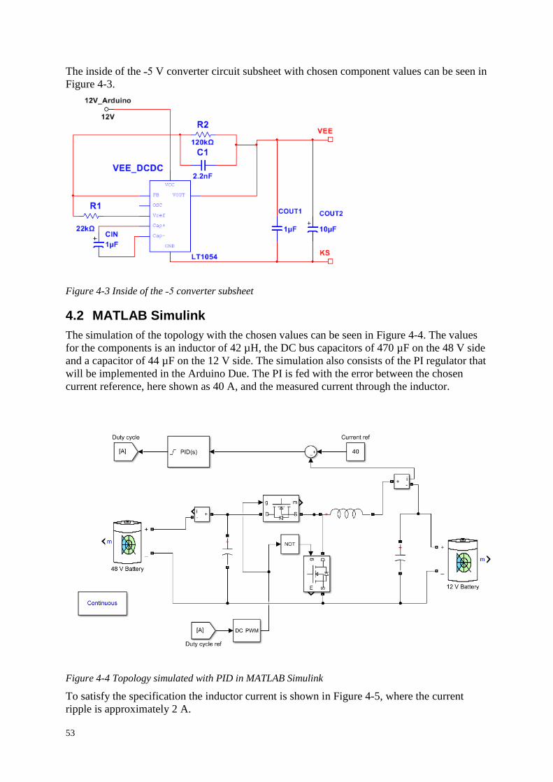
53
The inside of the ˗5 V converter circuit subsheet with chosen component values can be seen in
Figure 4-3.
Figure 4-3 Inside of the ˗5 converter subsheet
4.2 MATLAB Simulink
The simulation of the topology with the chosen values can be seen in Figure 4-4. The values
for the components is an inductor of 42 µH, the DC bus capacitors of 470 µF on the 48 V side
and a capacitor of 44 µF on the 12 V side. The simulation also consists of the PI regulator that
will be implemented in the Arduino Due. The PI is fed with the error between the chosen
current reference, here shown as 40 A, and the measured current through the inductor.
Figure 4-4 Topology simulated with PID in MATLAB Simulink
To satisfy the specification the inductor current is shown in Figure 4-5, where the current
ripple is approximately 2 A.
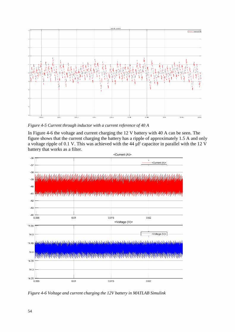
54
Figure 4-5 Current through inductor with a current reference of 40 A
In Figure 4-6 the voltage and current charging the 12 V battery with 40 A can be seen. The
figure shows that the current charging the battery has a ripple of approximately 1.5 A and only
a voltage ripple of 0.1 V. This was achieved with the 44 µF capacitor in parallel with the 12 V
battery that works as a filter.
Figure 4-6 Voltage and current charging the 12V battery in MATLAB Simulink
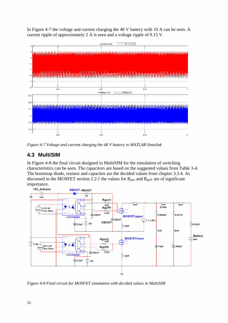
55
In Figure 4-7 the voltage and current charging the 48 V battery with 10 A can be seen. A
current ripple of approximately 2 A is seen and a voltage ripple of 0.15 V.
Figure 4-7 Voltage and current charging the 48 V battery in MATLAB Simulink
4.3 MultiSIM
In Figure 4-8 the final circuit designed in MultiSIM for the simulation of switching
characteristics can be seen. The capacitors are based on the suggested values from Table 3-4.
The bootstrap diode, resistor and capacitor are the decided values from chapter 3.3.4. As
discussed in the MOSFET section 2.2.1 the values for Rgon and Rgoff are of significant
importance.
Figure 4-8 Final circuit for MOSFET simulation with decided values in MultiSIM
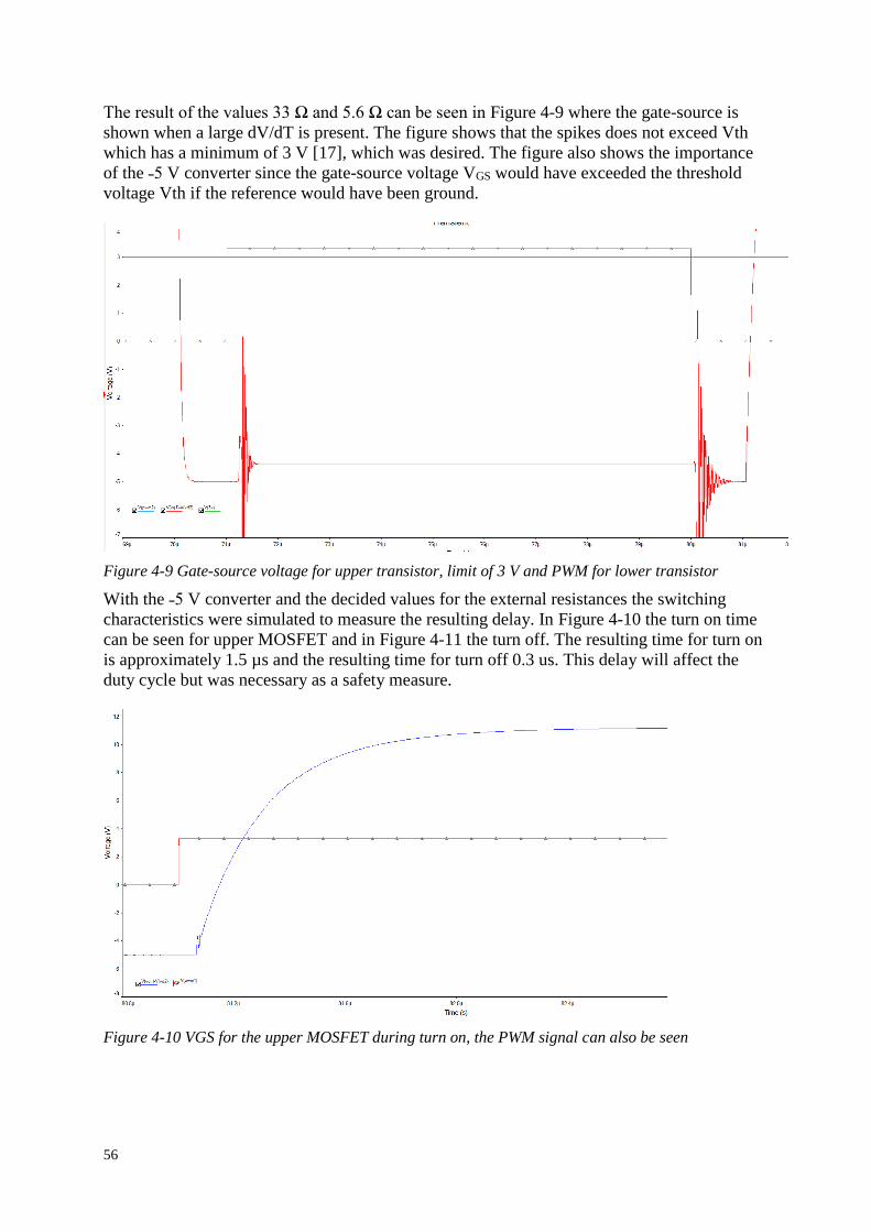
56
The result of the values 33 Ω and 5.6 Ω can be seen in Figure 4-9 where the gate-source is
shown when a large dV/dT is present. The figure shows that the spikes does not exceed Vth
which has a minimum of 3 V [17], which was desired. The figure also shows the importance
of the ˗5 V converter since the gate-source voltage VGS would have exceeded the threshold
voltage Vth if the reference would have been ground.
Figure 4-9 Gate-source voltage for upper transistor, limit of 3 V and PWM for lower transistor
With the ˗5 V converter and the decided values for the external resistances the switching
characteristics were simulated to measure the resulting delay. In Figure 4-10 the turn on time
can be seen for upper MOSFET and in Figure 4-11 the turn off. The resulting time for turn on
is approximately 1.5 µs and the resulting time for turn off 0.3 us. This delay will affect the
duty cycle but was necessary as a safety measure.
Figure 4-10 VGS for the upper MOSFET during turn on, the PWM signal can also be seen
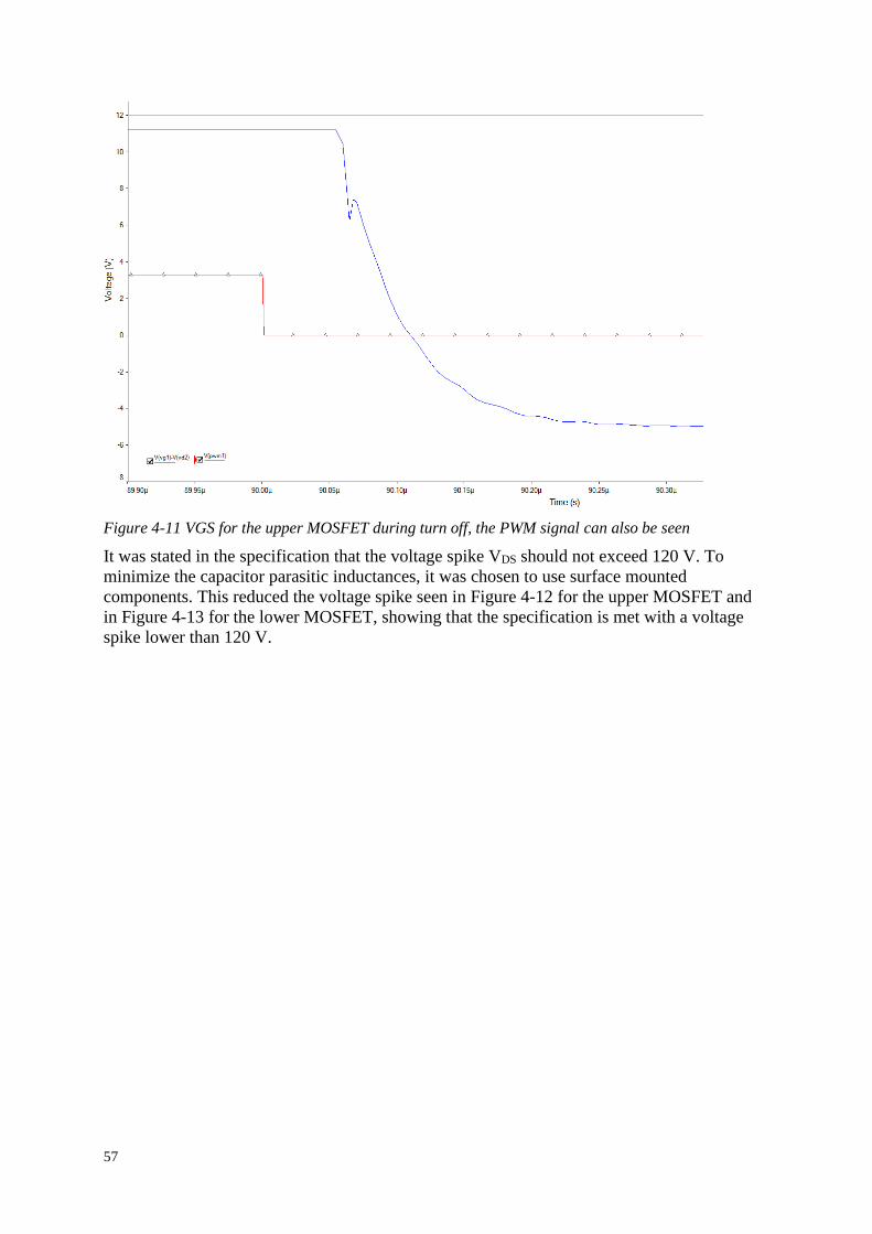
57
Figure 4-11 VGS for the upper MOSFET during turn off, the PWM signal can also be seen
It was stated in the specification that the voltage spike VDS should not exceed 120 V. To
minimize the capacitor parasitic inductances, it was chosen to use surface mounted
components. This reduced the voltage spike seen in Figure 4-12 for the upper MOSFET and
in Figure 4-13 for the lower MOSFET, showing that the specification is met with a voltage
spike lower than 120 V.
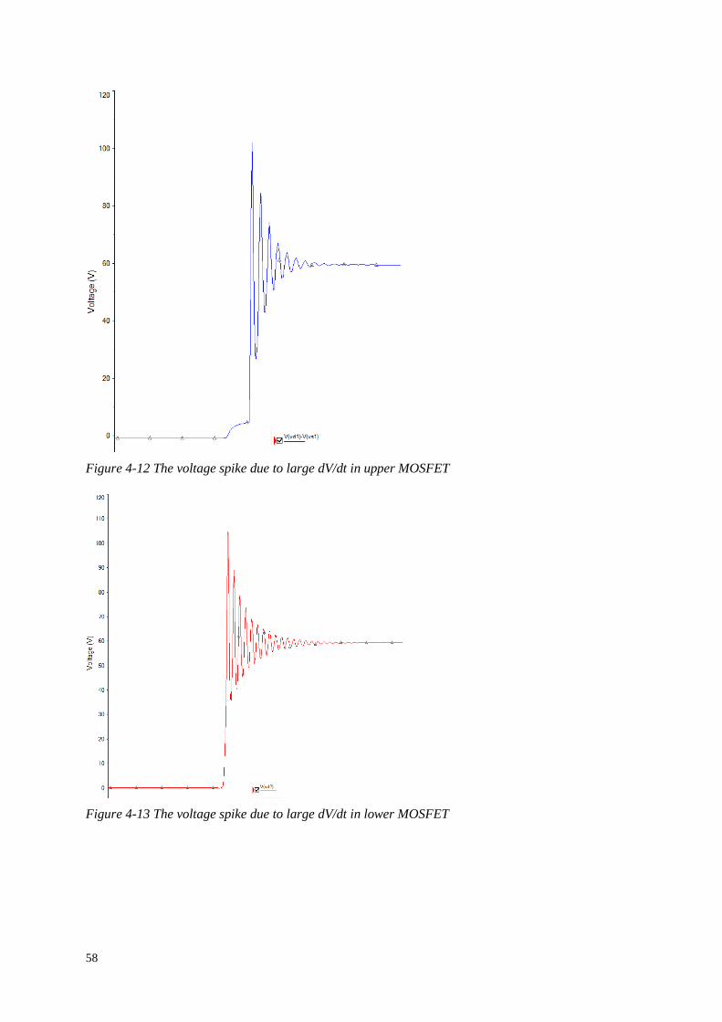
58
Figure 4-12 The voltage spike due to large dV/dt in upper MOSFET
Figure 4-13 The voltage spike due to large dV/dt in lower MOSFET

59
4.4 Efficiency
With the power losses calculated in section 3.X the proposed efficiency can be calculated as
𝜂 =
𝑃𝑂𝑈𝑇
𝑃𝐼𝑁=
𝑃𝐼𝑁 − 𝑃𝑙𝑜𝑠𝑠−𝑡𝑜𝑡𝑎𝑙
𝑃𝐼𝑁=
(12 ⋅ 40) − 28.313
12 ⋅ 40= 94.1 %
(4-1)
where Pin is calculated based on the same operation as the power losses. This operation being
the operation with a voltage of 12 V and a current of 40 A.
4.5 PCB
A three-dimensional image of the final PCB design can be seen in Figure 4-14. Not all
footprints used in the project consists of the correct dimensions in 3D.
Figure 4-14 3D preview of PCB design
4.6 Software Test
To test with the Simulink software, the simulation ran in continuous mode which means that
the Arduino Due and Simulink are connected during the test. Therefore, it is possible to
change constants and to measure the analog signals from the Arduino with a computer.
Constant current and constant voltage charge was both simulated with buck and with boost
mode with the step responses documented. In all the figures the time scale is one second per
square. In Figure 4-15 constant current regulation is used during boost mode when the
reference current is changed from 2 A to 5 A.
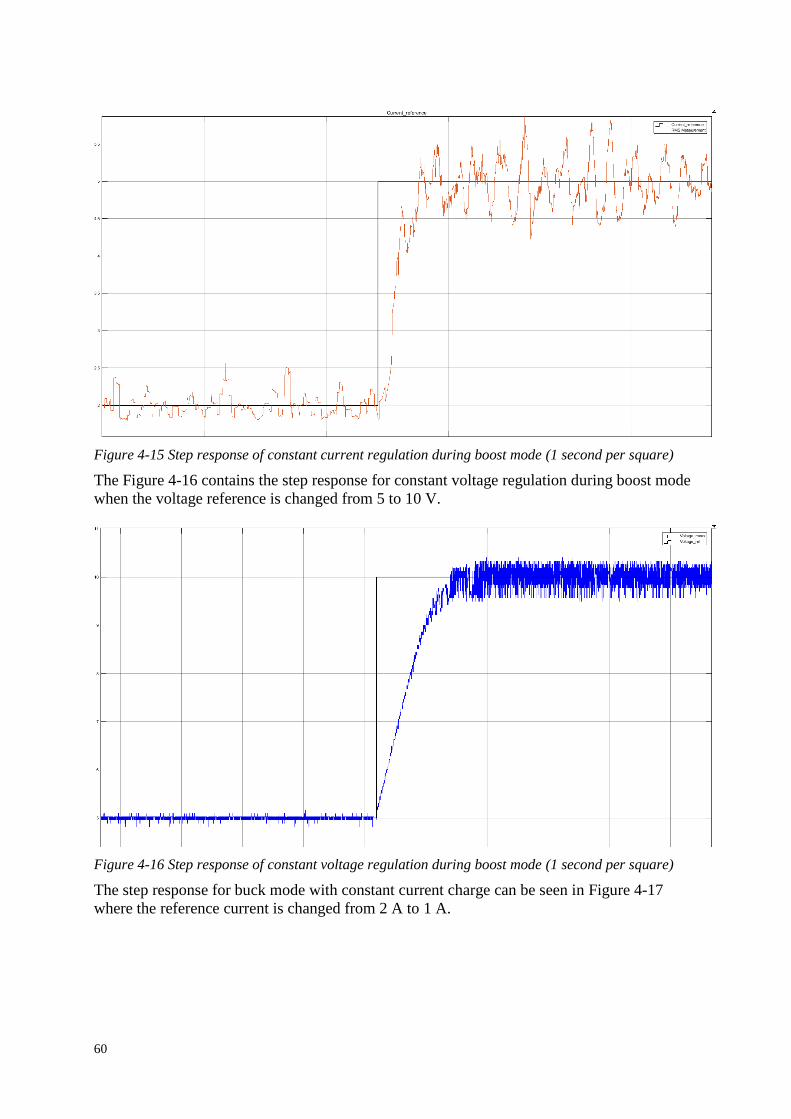
60
Figure 4-15 Step response of constant current regulation during boost mode (1 second per square)
The Figure 4-16 contains the step response for constant voltage regulation during boost mode
when the voltage reference is changed from 5 to 10 V.
Figure 4-16 Step response of constant voltage regulation during boost mode (1 second per square)
The step response for buck mode with constant current charge can be seen in Figure 4-17
where the reference current is changed from 2 A to 1 A.
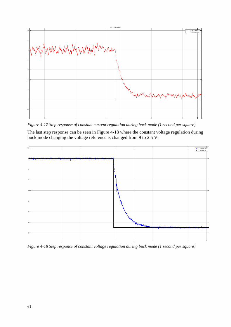
61
Figure 4-17 Step response of constant current regulation during buck mode (1 second per square)
The last step response can be seen in Figure 4-18 where the constant voltage regulation during
buck mode changing the voltage reference is changed from 9 to 2.5 V.
Figure 4-18 Step response of constant voltage regulation during buck mode (1 second per square)

62
5 Discussion The purpose of the discussion chapter is to evaluate the chosen method, the chosen sources of
information, the results and the overall project. During the ten weeks of the project many
changes occurred because of different reasons, these will be discussed. A discussion of the
project from an ethical point of view is also provided.
5.1 Result
In chapter result contains the consequences from the method in an objective manner. These
results will be discussed and analyzed.
5.1.1 Simulations
The results from simulations contains figures with the calculated values from the method. The
simulation in Simulink shows that the topology is suited for our application. The calculated
value of 42 µH for the inductor concludes in small ripple of only 2 A. The capacitor decreases
both the current and voltage ripple even further this is very promising for improving the
battery lifespan. A smaller ripple also means that the computing of current RMS will be
simpler.
The results from the simulations in MultiSIM were focused on the properties and
characteristics of the MOSFET. The simulations show that considerations have been made to
prevent false turn-on and overvoltage. The rise and fall time for the MOSFET provided in the
result is sufficient for our application with a switching frequency of 50 kHz and a voltage gain
of four.
5.1.2 Software
The software results indicate that the PI regulator can achieve constant current and constant
voltage for both buck and boost mode, however further improvement is possible. With more
time and effort better values for the PI coefficients can be found and a more accurate current
sensor can be used to increase stability. Due to time limitations this was not in the scope of
this project, however improvements can be implemented in the future. It should be noted that
the Arduino will use computing power during continuous simulation mode with Simulink for
communication which is detrimental to the test bench results. The software can definitely be
further optimized.
5.1.3 Efficiency
The part about efficiency can be criticized since it is not guaranteed that the efficiency is the
same for all power levels. It is also hard to say if the proposed design for the PCB could reach
the same efficiency since the calculations for power losses are simplified.
5.1.4 PCB
The final results of the PCB design in Ultiboard shows that the PCB is shared between the
DC/DC converter and the BLDC-inverter. The decision to do this was that this opened the
possibility of sharing a single 475 µF capacitor on the 48 V DC bus of both the motor inverter
and the DC/DC converter. This would minimize the risk oscillations that could occur with two
systems connected to the 48 V battery with long cables. The shared PCB also makes the
system more compact and easier to implement on the yacht.

63
The results were heavily affected by time limitations since only a proposed design of the PCB
is provided and not an actual analysis of the created PCB. This means that the results only rely
on the simulations results and results from the test bench. In turn, this can be criticized since
the chosen components cannot be analyzed and a conclusion about the performance cannot be
drawn.
5.2 Method
The used method in this project will both be discussed and criticized to defend and explain
why different decisions were made.
5.2.1 Pre-study
The test case in the energy calculations uses values that are approximated so it should be
noted that it is possible if for example more power is generated than consumed the power
conversion might be turned off in the actual system. It also suggests a simple energy transfer
strategy, but no evaluation of an implementation has been made on this because of time
limitations.
The pre-study only compares two topologies that were analyzed amongst the many more that
might do the job, however due to time limitations the more common full-bridge and half-
bridge topologies were chosen for comparison.
5.2.2 Simulation
It should be kept in mind that the simulation in the method is not guaranteed to perfectly
represent the real situation. Especially the simulation in Simulink that consider the
components to be ideal, however it works well as a proof of concept since these simulations
focus on control dynamics where the fast switching can be considered as ideal. The
simulations in MultiSIM was improved in this manner due to the produced models by the
manufacturers.
5.2.3 Components and Design
Many of the chosen components were chosen due to circumstances and limitation. A project
stretched over 10 weeks implies a limitation to the number of components that can be
analyzed and chosen between.
The method of choosing to build the inductor and wind it by hand can be criticized since the
component might not work exactly as intended. The margin of error can be considered to be
larger when the component is not thoroughly tested before use. This was however a
consequence of the limitations due to the available suppliers not stocking a suitable inductor
and having a custom-made being too expensive.
The decision of having the inductor outside of the PCB was due to the possibility of lowering
the temperature on the PCB by using a separate heatsink for the inductor. To place the
inductor outside of the PCB was also to minimize the noise and interference from the large
magnetic field of the inductor.
The heat sink was designed for an ambient temperature of 30 which will not always be the
case, since the system is implemented on a boat in a box that might have a different
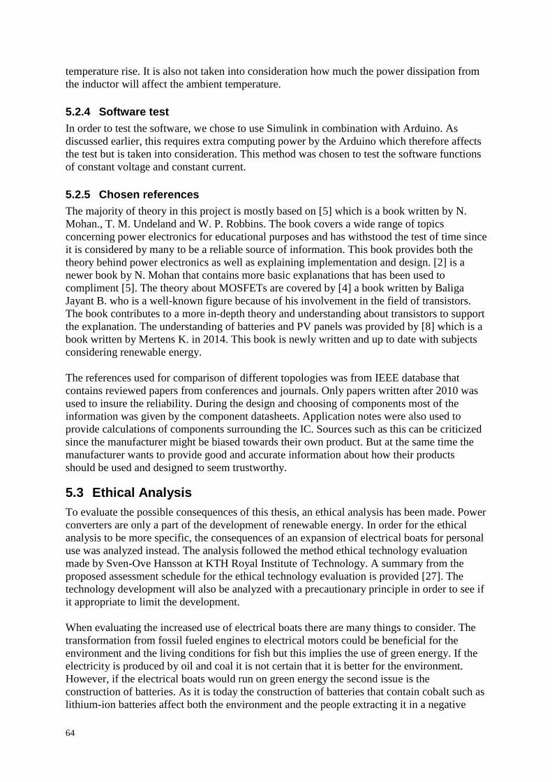
64
temperature rise. It is also not taken into consideration how much the power dissipation from
the inductor will affect the ambient temperature.
5.2.4 Software test
In order to test the software, we chose to use Simulink in combination with Arduino. As
discussed earlier, this requires extra computing power by the Arduino which therefore affects
the test but is taken into consideration. This method was chosen to test the software functions
of constant voltage and constant current.
5.2.5 Chosen references
The majority of theory in this project is mostly based on [5] which is a book written by N.
Mohan., T. M. Undeland and W. P. Robbins. The book covers a wide range of topics
concerning power electronics for educational purposes and has withstood the test of time since
it is considered by many to be a reliable source of information. This book provides both the
theory behind power electronics as well as explaining implementation and design. [2] is a
newer book by N. Mohan that contains more basic explanations that has been used to
compliment [5]. The theory about MOSFETs are covered by [4] a book written by Baliga
Jayant B. who is a well-known figure because of his involvement in the field of transistors.
The book contributes to a more in-depth theory and understanding about transistors to support
the explanation. The understanding of batteries and PV panels was provided by [8] which is a
book written by Mertens K. in 2014. This book is newly written and up to date with subjects
considering renewable energy.
The references used for comparison of different topologies was from IEEE database that
contains reviewed papers from conferences and journals. Only papers written after 2010 was
used to insure the reliability. During the design and choosing of components most of the
information was given by the component datasheets. Application notes were also used to
provide calculations of components surrounding the IC. Sources such as this can be criticized
since the manufacturer might be biased towards their own product. But at the same time the
manufacturer wants to provide good and accurate information about how their products
should be used and designed to seem trustworthy.
5.3 Ethical Analysis
To evaluate the possible consequences of this thesis, an ethical analysis has been made. Power
converters are only a part of the development of renewable energy. In order for the ethical
analysis to be more specific, the consequences of an expansion of electrical boats for personal
use was analyzed instead. The analysis followed the method ethical technology evaluation
made by Sven-Ove Hansson at KTH Royal Institute of Technology. A summary from the
proposed assessment schedule for the ethical technology evaluation is provided [27]. The
technology development will also be analyzed with a precautionary principle in order to see if
it appropriate to limit the development.
When evaluating the increased use of electrical boats there are many things to consider. The
transformation from fossil fueled engines to electrical motors could be beneficial for the
environment and the living conditions for fish but this implies the use of green energy. If the
electricity is produced by oil and coal it is not certain that it is better for the environment.
However, if the electrical boats would run on green energy the second issue is the
construction of batteries. As it is today the construction of batteries that contain cobalt such as
lithium-ion batteries affect both the environment and the people extracting it in a negative

65
manner. However, the development and knowledge about batteries is increasing and hopefully
is a solution to that problem will be found.
To enforce this change, campaigns such as the one mentioned in the background might be
needed to speed up the process. To compare with the electrical car the big change came when
the company Tesla made big investments to speed up this process and to produce their own
electrical cars. A change like that and further development of PV panels might be the
condition for a rapid change to help our environment and lower the carbon emissions.

66
6 Conclusions In this study, a design was suggested for a synchronous bidirectional half-bridge buck-boost
converter used in a dual battery application. A software required to control it has been
proposed as well as a design for a PCB implementation. Suggested components and thermal
considerations were also made for the design of 40 A charge capability. A strategy for energy
transfer seen in Figure 3-3 has been proposed but not evaluated due to time limitations. In the
results, the simulations show that the converter design can work as means of bidirectional
energy transfer. This was tested by using a test-bench which shows that the software is
capable of controlling the converter to achieve constant current and constant voltage during
both buck and boost mode.
For future work this system could be tested using a manufactured PCB that can be
implemented in a yacht to evaluate the performance and design choices. This would provide a
possibility to carry out a field test that could better show what the actual power flow is to
compare with the test case in the energy calculations. In addition, the software can be
developed to improve the regulation during constant voltage and constant current. With more
in-depth research of the chosen batteries, better charging and discharging techniques may be
found. The hardware can be improved to allow a more accurate and complex calculation of
the SoC to be implemented.
67
7 References
[1] Regeringskansliet, “Ny klimatsatsning - regeringen föreslår premie för
elutombordare”, Regeringskansliet, April 2018. [Online]. Available:
https://www.regeringen.se/pressmeddelanden/2018/04/ny-klimatsatsning---regeringen-
foreslar-premie-for-elutombordare/. [Accessed: June 2018].
[2] Mohan N., “Power Electronics: a first course”, 1st edition, New Jersey:John Wiley &
Sons; 2011.
[3] Chao K., Tseng M., Huang C., Liu Y. and Huang L., “Design and Implementation of a
Bidirectional DC/DC Converter for Stand-Alone Photovoltaic Systems”, International
Journal of Computer, Consumer and Control, Vol. 2, No.3, 2013.
[4] Baliga Jayant B. “Fundamentals of Power Semiconductor Devices”, 1st edition, New
York: Springer US; 2008.
[5] Mohan N., Undeland T.M. and Robbins W.P., “Power Electronics, Converters,
Applications, and design”, 3rd edition. New Jersey: John Wiley & Sons Ltd; 2003.
[6] Vishay, Device Appl. Note AN608A, pp. 1-6.
[7] Texas Instruments, Appl. Note SLVA535A, pp. 3˗5.
[8] Mertens K. “Photovoltaics Fundamentals, Technology and Practice”, 1st edition, New
Jersey: John Wiley & Sons Ltd; 2014.
[9] Baccouche I., Mlayah A., Jemmali S., Manai B. and Essoukri Ben Amara N.,
"Implementation of a Coulomb counting algorithm for SOC estimation of Li-Ion
battery for multimedia applications," 2015 IEEE 12th International Multi-Conference
on Systems, Signals & Devices (SSD15), Mahdia, 2015
[10] Qazi S., “Standalone Photovoltaic (PV) Systems for Disaster Relief and Remote
Areas”, 1st edition, Amsterdam: Elsevier; 2016
[11] ON Semiconductor, Appl. Note AN-6076, pp.1-4.
[12] NASA (2017), “Engineering Design“, NASA, November 7, 2017. [Online].
Available: https://mynasadata.larc.nasa.gov/engineering-design/.[Accessed: June
2018]
[13] Ioinovici A., “Power electronics and energy conversion systems”, 1st edition,
Chichester:John Wiley & Sons Ltd; 2013
[14] Yu Z., Kapels H. and Hoffmann K. F., “A Novel Control Concept for High-
Efficiency Power Conversion with the Bidirectional Non-inverting Buck-Boost
Converter”, 2016 18th European Conference on Power Electronics and Applications
(EPE'16 ECCE Europe), Karlsruhe, 2016.
68
[15] Ouchi T., Kanouda A., Takahashi N. and Moteki M. , "Seamless controlled parallel
bi-directional DC/DC converter for energy storage system" 2014 16th European
Conference on Power Electronics and Applications, Lappeenranta, 2014
[16] Xu X., Zheng C., Hu C., Lu Y. and Wang Q., "Design of Bi-directional DC/DC
converter," 2016 IEEE 11th Conference on Industrial Electronics and Applications
(ICIEA), Hefei, 2016
[17] Infineon, “OptiMOS™ 5 Power-Transistor 150V”, IPB044N15N5 datasheet, April
2016 [Revised April 2016].
[18] Texas Instruments, “Single-Channel Isolated Gate Drivers” UCC5390SC datasheet,
June 2017 [Revised May 2018].
[19] Texas Instruments, “Switched-Capacitor Voltage Converters With Regulators”
LT1054 datasheet, Feb. 1990 [Revised July. 2015].
[20] Allegro, Appl. Note A3946, pp.7-9.
[21] Vishay, “Long Side Termination Thick Film Chip Resistors” RCL e3 datasheet, Feb.
2017 [Revised July. 2017].
[22] Comchip, “SMD Schottky Barrier Rectifiers” CDBC5150-HF datasheet [Rev.B].
[23] TDK, “Ferrites and accessories” SIFERRIT material N27 datasheet, May. 2017
[Revised May 2017].
[24] CircuitCalculator.com, “PCB Via Calculator”, CircuitCalculator.com, Mars, 2006.
[Online]. Available: http://circuitcalculator.com/wordpress/2006/03/12/pcb-via-
calculator/ [Accessed: June 2018].
[25] CircuitCalculator.com, “PCB Trace Width Calculator”, CircuitCalculator.com,
January, 2006. [Online]. Available
http://circuitcalculator.com/wordpress/2006/01/31/pcb-trace-width-calculator/
[Accessed: June 2018].
[26] Atmel, “SMART ARM-based MCU” SAM3X8E ARM Cortex-M3 datasheet, Feb.
2017 [Revised Mars 2015].
[27] Hansson S. O., “Teknik och etik”, KTH University Philosophy department, 2009.

69
8 Appendix
8.1 Batteries Used in Project
8.1.1 12 V lead-acid battery
Existing in the boat is a set of four parallel 12 V VRLA batteries. The batteries are of the type
PartSmart Maringel MG3120. The table below is summarizing the battery data:
Unit Bank
Nominal voltage V 12 12
Max voltage V 14.4 14.4
Rated capacity Ah 96 384
Maximum DoD % 60
Stored energy Wh 2765
Max charging current A 38
Recommended charge current A 9.6
Recommended charge voltage V 14.4-14.6
8.1.2 48 V LiFePo4 battery
The 48 V battery system is based on LiFePo4 high power cells from EV (GWL) Power. The
battery bank is built by 16 series connected 3.2 V, 60 Ah cell modules. A battery management
system from EV-Power will be used which includes balancing between cells as well as
isolating contactors, protecting from over charging and deep discharge. The depth of
discharge is limited to 75%.
No of cells 16
Q Ah 60
Imax A 180
Unom V 51.2
Umax V 60.8
Umin V 40
Ri Ω 0.032
Wbat Wh 2304
Weight kg 27
Volume l 15

70
8.2 PV panels used in project
There are two PV panels that will be used to generate power to the 12 V battery. The
specifications for standard test conditions are written below.
PV1
Name: Solara SM 160 M
Pmax: 40 W
Umax: 16.7 V
Imax: 2.2 A
PV2
PPAM Onyxium 145W
Pmax: 144 W
Umax 16.62 V
Imax: 8.64 A