Embed Size (px)
Citation preview
Designing and Assembling a Universal USB Power Supply Aaron Lee
Dr. James Dann Applied Science Research, Menlo School
May 17, 2017
I. Abstract A 120V AC to 5V DC power supply was designed and constructed in the Whitaker Lab
of Menlo School to interface with any mobile USB device. USB was used as it is the most universal interface for power delivery to modern electronic devices, allowing the power supply to work with the widest range of mobile devices. The power supply is capable of charging four devices with a total power output of up to 20W at an average efficiency of 38.8%.
Lee 1
II. Table of Contents
I. Abstract Title Page II. Table of Contents 1
III. Introduction 2 A. Electrical Power Transmission 2 B. Power Supplies 3
IV. Theory 5 A. Alternating Current 5 B. Power Transformers 6 C. Diodes and Rectifiers 7 D. Capacitors 10 E. Voltage Regulators 11 F. Electrical Fuses 13
V. Design 14 A. Circuity Functionality 14 B. Physical Unit Assembly and Design 15
VI. Next Steps 18 VII. Results 19
VIII. Conclusion 19 IX. Acknowledgements 20 X. Works Cited 21
XI. Appendices 22 A. Parts List and Costs 22 B. LM338 Internal Functional Block Diagram 23 C. TPS2513EVM-527 Internal Functional Diagram 23 D. Dimensioned Drawings of Power Supply Unit Design 24
Lee 2
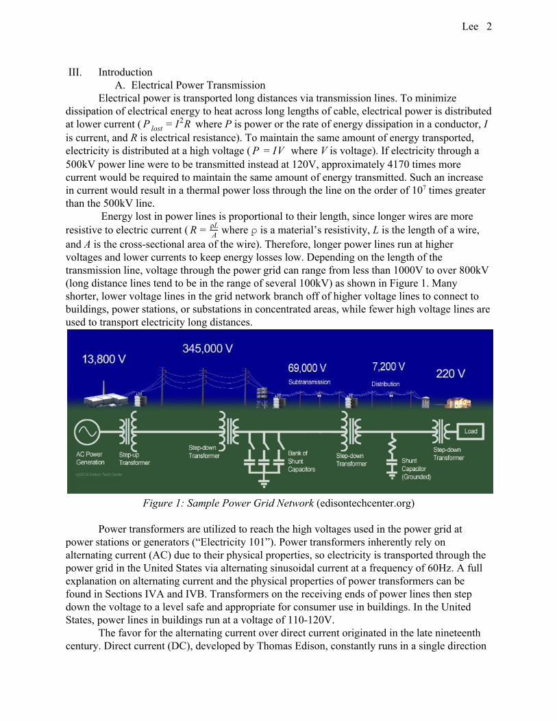
III. Introduction A. Electrical Power Transmission
Electrical power is transported long distances via transmission lines. To minimize dissipation of electrical energy to heat across long lengths of cable, electrical power is distributed at lower current ( where P is power or the rate of energy dissipation in a conductor, IRP lost = I2 is current, and R is electrical resistance). To maintain the same amount of energy transported, electricity is distributed at a high voltage ( where V is voltage). If electricity through aVP = I 500kV power line were to be transmitted instead at 120V, approximately 4170 times more current would be required to maintain the same amount of energy transmitted. Such an increase in current would result in a thermal power loss through the line on the order of 107 times greater than the 500kV line.
Energy lost in power lines is proportional to their length, since longer wires are more resistive to electric current ( where is a material’s resistivity, L is the length of a wire,R = A
ρL and A is the cross-sectional area of the wire). Therefore, longer power lines run at higher voltages and lower currents to keep energy losses low. Depending on the length of the transmission line, voltage through the power grid can range from less than 1000V to over 800kV (long distance lines tend to be in the range of several 100kV) as shown in Figure 1. Many shorter, lower voltage lines in the grid network branch off of higher voltage lines to connect to buildings, power stations, or substations in concentrated areas, while fewer high voltage lines are used to transport electricity long distances.
Figure 1: Sample Power Grid Network (edisontechcenter.org)
Power transformers are utilized to reach the high voltages used in the power grid at
power stations or generators (“Electricity 101”). Power transformers inherently rely on alternating current (AC) due to their physical properties, so electricity is transported through the power grid in the United States via alternating sinusoidal current at a frequency of 60Hz. A full explanation on alternating current and the physical properties of power transformers can be found in Sections IVA and IVB. Transformers on the receiving ends of power lines then step down the voltage to a level safe and appropriate for consumer use in buildings. In the United States, power lines in buildings run at a voltage of 110-120V.
The favor for the alternating current over direct current originated in the late nineteenth century. Direct current (DC), developed by Thomas Edison, constantly runs in a single direction
Lee 3
at an often stable voltage. Alternating current, favored by Nikola Tesla, varies with a sinusoidal voltage which reverses current flow for half a period. While DC electricity is much more stable and easy to use for small electrical and electronic devices, it is less flexible for widespread distribution than AC electricity, which can be easily converted to higher or lower voltages with transformers. At the time, AC electricity also was the natural signal output by Tesla’s polyphase induction motors. When these were used to harness power from hydroelectric dams, it was most efficient to transmit the electricity in its natural AC form. These advantages allowed AC electricity to be distributed more cheaply than DC, resulting in greater development and investment into AC transmission as the use of electricity and the need for a grid to transport it grew (Lantero).
The flexibility and investment into AC electricity coincided with a growing electrical distribution system or “grid” in the United States near the turn of the century. At the time, such systems were quite small and localized, connecting consumers only to nearby power plants. With additional research and resources over the decades of the twentieth century, the electrical system began to grow, interlocking many small grids together for greater reliability and distribution of power where needed, reducing outages and wasted energy. The electrical distribution system reached its peak of interconnectedness, close to as it exists today, in the 1960s (“Electricity 101”).
High voltage DC (HVDC) power lines are also used to transport electricity very long distances, such as between countries and across large bodies of water. These are the result of modern technology that allows for efficient electrical rectification (conversion of AC to DC) and inversion (conversion of DC to AC). DC transmission is more efficient across long distances because lines do not need to be designed to sustain the peak amplitude voltages of AC. The same amount of energy can be transported at the RMS rated voltage of an AC signal with a constant DC voltage, or more energy can be transported with a constant DC voltage equal to the peak amplitude voltage through the same cable. For example, a power line designed to transmit 500kV AC must be able to sustain peak amplitude voltages of about 707kV. The same line could be used to transport DC electricity at a constant 707kV, a significant increase in the energy transported with the same material. Similarly, the same amount of energy in a 500kV AC line could be transported with a 500kV DC voltage, but the cable would only need to be designed to sustain 500kV and not the peak 707kV of the AC signal, making it cheaper. However, since power transformers cannot be used to reach high DC voltages, high AC voltages must be converted to DC for high voltage DC transmission. At the other end of HVDC lines, DC electricity must also be converted back into AC to connect to the already developed AC grid. Equipment to handle the rectification and inversion process at such high voltages is very expensive, still developing, and relatively inefficient, making the advantages of HVDC only practical for very long linear power lines, not for interconnecting a grid. Multiple HVDC lines exist across North America, and many are used in Europe and Asia for connecting countries like the United Kingdom and Japan across bodies of water (Harnden).
B. Power Supplies A power supply is a device that connects to the 110-120V electrical lines in buildings and
converts the high voltage AC electricity into lower voltage DC electricity that can be easily and efficiently utilized by electrical devices. Power supplies are constructed from several smaller electrical and/or electronic components. The primary components to a power supply are

Lee 4
transformer, rectifier, filter, and regulator systems. The transformer steps down the 110-120V AC voltage to the appropriate voltage to be used by everyday electronic devices. The rectifier, typically consisting of diodes, reverses back current in AC electricity so that all current flows in one direction. A filter, typically consisting of capacitors, smooths out the sinusoidal wave of the AC current into a steadier flow of current closer to a constant voltage. Lastly, a voltage regulator further smooths out the output to a constant voltage and prevents surges or spikes in current from damaging anything connected to the DC output of the supply. Greater explanation of each of these components and how they accomplish their respective goals can be found in Section IV.
Commercial power supplies for consumers developed in the early 1920s as simple products to eliminate the need for disposable batteries used in small, relatively low power electronic devices such as radios. An ad for one such “‘B’ Battery Eliminator” is shown in Figure 2. However, in the 1930s such devices began to include unique or built-in power supplies to connect directly to the power lines in homes instead of relying on batteries. Power supplies have been designed and manufactured uniquely for separate electronic products ever since, eliminating the need for external or modular power supplies (Toich).
Figure 2: 1920s “‘B’ Battery Eliminator” Advertisement (antiqueradios.com)
With the rise of mobile electronics, devices such as smartphones and laptops have kept
power supplies in external “bricks” to reduce their carrying weight and volume. Since mobile devices, particularly smartphones and tablets, mostly nearly all interface with USB for power delivery, individual power bricks can be combined into a single power supply.
All modern USB devices charge at 5V; however, each requires a unique data signal to instruct it to draw current from its power supply determined by the manufacturer. Therefore, each must have its own power supply or adapter to power it. All of these unique chargers, as well
Lee 5
as portable battery banks or other charging devices, add effective weight and volume to mobile devices, which are designed to be lightweight, portable, and easy to use on the go. Each added power supply also adds redundant components to the mass of the device. Most of the process can be combined into a single, much more modular and flexible power supply. IV. Theory
A. Alternating Current Alternating current runs at a varying sinusoidal voltage with a frequency of 60Hz in the
United States. The voltage of AC electricity is expressed as the root mean square voltage of the sinusoidal wave, because at this voltage DC electricity is capable of doing the same amount of work as the AC electricity.
Since the voltage of AC electricity varies sinusoidally, the root mean square voltage can
be expressed as , where T is the period of the signal, Vmax is the V RMS = √ cos (ωt) dt1T ∫
T
0V 2
max2
amplitude of the signal, and is the angular frequency of the signal. Substituting for andT2π
evaluating the given integral yields the result (Scherz 20-21). Therefore, the peakV RMS = √2V max
voltage of a 120V AC signal would be about 170V.
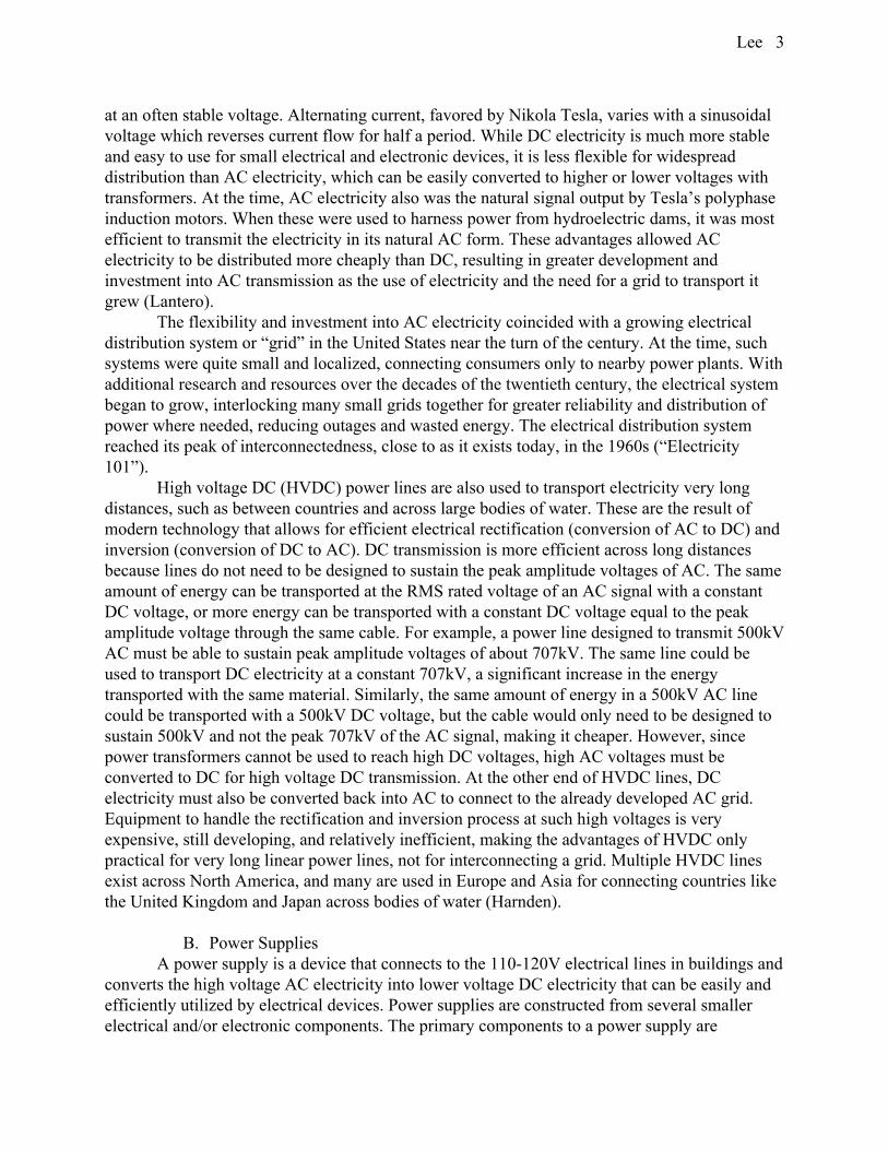
B. Power Transformers
Figure 3: Power Transformer Components (amaderelectronics.com)
A transformer is a device used to convert AC voltages to higher or lower values. A
transformer typically consists of an iron core and two coils of wire, each with a terminal connected to each end. Each coil is wound a certain number of times around the two ends of the core, as shown in Figure 3. The two coils are referred to as the primary and secondary coils. The input voltage is connected across the primary coil. Current flow through the coil creates a strong magnetic field through the center of the coil. The iron core strongly focuses the magnetic field
Lee 6
from the primary coil through the secondary coil, due to the high permeability and inductance of iron (“Magnetic Properties of Solids”). Therefore, nearly all of the magnetic flux created by the primary coil is channeled through the secondary coil.
According to Faraday’s law of electromagnetic induction, the induced electromotive force or voltage in the secondary coil , where N is the number of loops in the coil andNε = − dt
dφ
is the time rate of change of magnetic flux through the coil. Since the induced voltage isdtdφ
proportional to the time rate of change of magnetic flux, transformers only work with AC voltages. DC connected to the primary coil would simply generate a constant magnetic flux through the secondary coil, inducing no voltage in the secondary coil except a little when it is connected and disconnected. The differential properties of sinusoids result in the same frequency voltage signal across the secondary coil of the transformer, with only a different amplitude.
Solving for from the above equation yields , where V2 is the voltage acrossdtdφ −dt
dφ = N2
V 2 the secondary coil and N2 is the number of loops in the secondary coil. Since nearly all of the magnetic flux from the primary coil passes through the secondary coil, can be equated in thedt
dφ primary and secondary loops, resulting in the relationship and the expression for theN1
V 1 = N2
V 2 effective voltage of the secondary coil , where N1 is the number of loops in theVV 2 = N1
N21
primary coil and V1 is the voltage across the primary coil. This proportionality allows AC voltages to be easily converted to specific higher or lower voltages based on the number of loops in each coil of a transformer (Scherz 112-113). The coils of a transformer can also be connected at different locations to effectively change the number of active coil loops. For example, a center-tapped secondary coil transformer allows it to output two voltages, one half the other, rather than just one with an electrical terminal connected to the center of the secondary coil.
Inefficiencies in transformers are due to hysteresis loss in the iron core, the induction of eddy currents within the iron core or surrounding materials, and heat loss due to the Ohmic resistance of the wires in the coils. Modern transformers are typically 95+% efficient at high and low voltages.
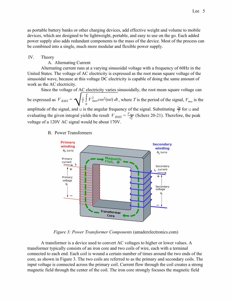
The ability to efficiently step down the 110-120V from the power grid with a transformer is essential for a power supply so that it can power devices that run at much lower, safer, and more efficient voltages. Figure 4 shows the 12V AC output of a Coast Electronic Supply 67-1245 transformer used in the power supply, which converts a primary AC voltage of 117V to either 12V or 24V with a center-tapped secondary coil. All voltage signals depicted were measured with an Agilent Technologies DSO1004A oscilloscope across a AVT50-10-ND 10Ω power resistor to simulate a load similar to that of the electronic devices that interface with the power supply. The input to the transformer was controlled with a TDGC2-2KVA variable transformer, which receives 110V AC and outputs 0-130V AC.
Lee 7
Figure 4: 67-1245 12V AC Output
C. Diodes and Rectifiers
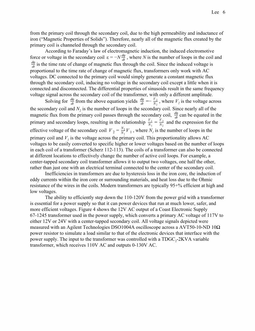
Figure 5: pn-Junction Diode Components (physics-and-radio-electronics.com)
Diodes are small semiconductive electrical devices that allow current to only flow one
direction through them. Diodes accomplish this effect by junctioning n-type and p-type semiconductive silicon plates together. Silicon has four valence electrons; however, n-type silicon is doped with phosphorus, which has five valence electrons. The addition of phosphorus into the silicon crystal creates an excess of free electrons in the crystal. Similarly, p-type silicon is doped with boron, which has three valence electrons, creating an excess of holes, or a lack of electrons, in the silicon crystal. In a standard silicon rectifier diode, p-type and n-type silicon plates are wedged together. The end of the diode connected to the p-type plate is the anode end, and the end connected to the n-type plate is the cathode end, as shown in Figure 5.
Due to the properties of the p-type and n-type silicon, current can only flow from the anode end to the cathode end of the diode. If a positive voltage is applied across the diode from the anode end to the cathode end, free electrons in the n-type silicon move towards the junction with the p-type, since electrons move against positive voltage and current flow. Similarly, the holes in the p-type silicon effectively “move” towards the junction with the n-type, as free
Lee 8
electrons in the p-type crystal will move away from the junction, leaving holes behind them. Electrons meeting holes at the junction decrease the depletion zone (a section of electrical insulation) between the two silicon crystals, allowing current to flow.
A voltage applied in the opposite direction creates no current flow through the diode. Free electrons in the n-type silicon and holes in the p-type silicon both move away from the junction, increasing the depletion zone between the plates and effectively diminishing electric conductivity between the two crystals (123-131).
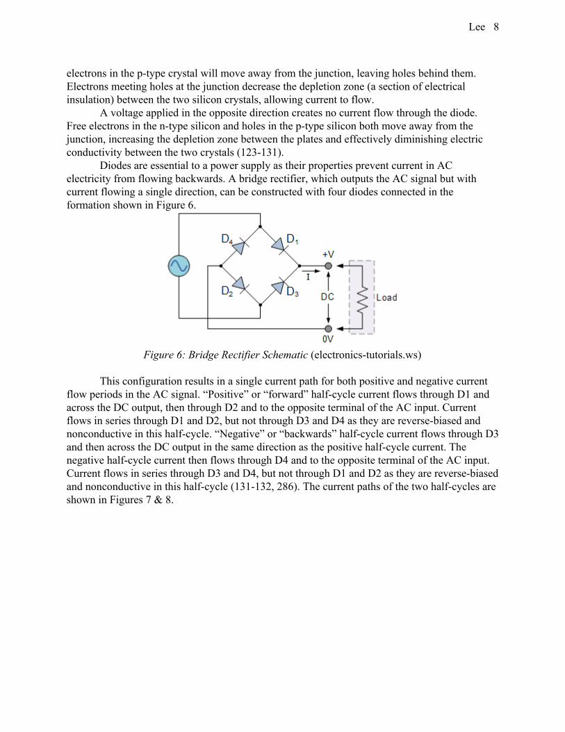
Diodes are essential to a power supply as their properties prevent current in AC electricity from flowing backwards. A bridge rectifier, which outputs the AC signal but with current flowing a single direction, can be constructed with four diodes connected in the formation shown in Figure 6.
Figure 6: Bridge Rectifier Schematic (electronics-tutorials.ws)
This configuration results in a single current path for both positive and negative current
flow periods in the AC signal. “Positive” or “forward” half-cycle current flows through D1 and across the DC output, then through D2 and to the opposite terminal of the AC input. Current flows in series through D1 and D2, but not through D3 and D4 as they are reverse-biased and nonconductive in this half-cycle. “Negative” or “backwards” half-cycle current flows through D3 and then across the DC output in the same direction as the positive half-cycle current. The negative half-cycle current then flows through D4 and to the opposite terminal of the AC input. Current flows in series through D3 and D4, but not through D1 and D2 as they are reverse-biased and nonconductive in this half-cycle (131-132, 286). The current paths of the two half-cycles are shown in Figures 7 & 8.

Lee 9
Figures 7 & 8: Respective Positive and Negative Half-Cycle Current Paths Through Bridge
Rectifier (electronics-tutorials.ws)
The output of a bridge rectifier is a sinusoid with all negative half-cycles reversed to be positive. Connecting the 12V output of the 67-1245 transformer to a bridge rectifier of four 6A 100V diodes to sustain the necessary voltages and current drawals of the power supply yields the output shown in Figure 9.
Figure 9: Bridge Rectifier Output

Lee 10
D. Capacitors
Figure 10: Basic Capacitor Use Case (ggspdt.com)
Capacitors are electrical devices designed to separate and store charge. They consist of
two parallel conducting plates placed close to each other, each connected to an electrical terminal. If a voltage is applied across a capacitor, electrons are drawn from one plate to the other. The capacitor sustains a charge and voltage as long as the applied voltage remains, as shown in Figure 10. Once this voltage is removed, the capacitor discharges as electrons move back from excess on one plate to balance between the two again, creating a current opposite the current that was created to charge it and a voltage initially beginning at the voltage that the capacitor was charged at (21).
The potential across a capacitor is exponentially related to time and the RC (resistance times capacitance, where capacitance , Q is the charge stored on the capacitor, and V isC = Q
V the voltage across the capacitor) time constant of the circuit it is connected to. If a discharged capacitor is connected to a constant electric potential, the voltage across it over time is modeled by where is the EMF of the potential the capacitor is connected to. If a(1 )V = ε − e−t/RC ε capacitor is charged and its terminals are connected, the voltage across it over time is modeled by where is the EMF that capacitor is charged to. However, since the voltage fromeV = ε −t/RC ε the rectifier is not constant and varies sinusoidally, these exponential relationships do not apply to a filter capacitor in a power supply.
Capacitors are essential for the filtering process in a power supply as they smooth out the wave output by the rectifier shown in Figure 9. A capacitor connected in parallel with the output of the rectifier charges at high voltages and discharges at lower voltages, altering the output to a much smoother, more consistent voltage slightly under the root mean square voltage of the original AC voltage due to voltage drops across the diodes in the rectifier.
A 50V 10000µF aluminum electrolytic capacitor is connected to the output of the bridge rectifier connected to the 12V output of the 67-1245 transformer, yielding the output shown in Figures 11 & 12.

Lee 11
Figures 11 & 12: Filter Capacitor Output, Respectively DC and AC Scale
While the output with a filter capacitor is much more steady, a significant ripple voltage
in the signal at the 120Hz frequency of the rectified AC signal is still present. As shown in Figure 12, the peak-to-peak ripple voltage of the output across the 10Ω load is about 1.08V. Ripple voltage output is affected by the frequency of the signal, load current drawn, and capacitance of the capacitor. The root mean square of the ripple voltage can be expressed as
. Therefore, higher capacitance filter capacitors minimize ripple voltage sinceV ripple(RMS) = fCI load
they store more charge at the same voltage (289-290). The 10000µF capacitor used brings the ripple voltage low enough for the next component of the power supply, the voltage regulator, as detailed in Section IVE.
E. Voltage Regulators
Figure 13: Basic Example Voltage Regulator Block Diagram (Scherz 284)
Voltage regulators are electrical devices that maintain a steady output voltage by
automatically altering output current. Linear voltage regulators accomplish this by monitoring
Lee 12
output voltage with a sample voltage given by a sampling circuit (two resistors in series). The voltage across the second resistor is connected to the base of the error amplifier, a transistor. A zener diode, which reverses its polarity at a specified voltage limit, is in place to keep a constant reference voltage for the error amplifier to compare against the sample voltage. The error amplifier then generates an error voltage between the sample voltage and the reference voltage. The error voltage is sent to the current control transistor, which then adjusts load current effectively. Each of these components is shown in Figure 13 (284).
In adjustable voltage regulators, sampling circuit components are removed and are instead connected externally, and the ground terminal is replaced by an adjustment terminal. By varying the resistances of the two resistors in the sampling circuit, the output voltage can be fine tuned to any voltage within a specified range determined by the thermal and input limits of the regulator and the external components.
Voltage regulators are essential to a power supply for keeping the output DC voltage constant and controlled. Voltage regulators minimize the ripple voltage output by the filter capacitors, prevent the output voltage from spiking under surges, and fine tune the output voltage to a constant desired value.
LM338 linear voltage regulators are used in the power supply because of their high 5A current limit. A complete functional diagram of the internal circuitry of the LM338 can be found in Section XI Appendix B.
The LM338 has a specified 60dB 120Hz ripple rejection ratio, meaning that it reduces the magnitude of a ripple voltage from a 120Hz signal by a factor of 10-3. This relationship is determined from the decibel scale for a ratio of output power to input power, -60dB
. Since power is proportional to voltage squared ( where V is voltage and0log ( )= 1 10 P in
P out P = RV 2
R is resistance), this statement can be modified for a ratio of output voltage to input voltage to -60dB . Solving for Vout in terms of Vin yields the result .0log ( )= 2 10 V in
V out VV out = 10−3in
Therefore, the given 1.08V peak-to-peak ripple voltage shown to be output by the filter capacitor in Section IVD results in a peak-to-peak ripple voltage output by the LM338 of 1.08mV, a very insignificant and acceptable amount. Therefore, the 10000µF capacitance of the filter capacitor is large enough to keep the ripple voltage low enough for the LM338 to handle. Additionally, connecting a 10µF bypass capacitor from the adjustment terminal to DC ground, as described in Section VA, improves the 120Hz ripple reduction ratio to 75dB (“LM338 5A Adjustable Output Linear Regulator”).
The output of the filter capacitors is connected to the input of an LM338. The output shown in Figures 14 & 15 is with the sampling circuit configured for the LM338 to output 5V DC. More explanation on the external components used with the LM338 how the LM338 was connected to the power supply circuit can be found in Section VA.
Lee 13
Figures 14 & 15: LM338 5V Output, Respective DC and AC Scale
As shown in Figures 14 & 15, the final output from the LM338 regulator is very steady at
the desired 5V. Peak-to-peak noise in the output signal is very small at a magnitude of less than 10mV or less than 0.2% of the output voltage. This tiny amount of noise is very insignificant and can likely be attributed as much to the precision of the oscilloscope used to measure the signal as to the output of the LM338. This regulated output and small margin of noise is very safe to connect to electronic devices.
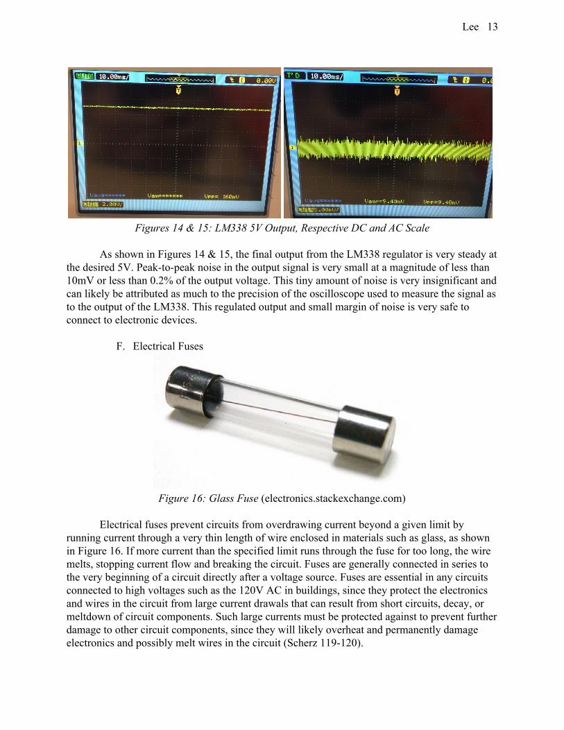
F. Electrical Fuses
Figure 16: Glass Fuse (electronics.stackexchange.com)
Electrical fuses prevent circuits from overdrawing current beyond a given limit by
running current through a very thin length of wire enclosed in materials such as glass, as shown in Figure 16. If more current than the specified limit runs through the fuse for too long, the wire melts, stopping current flow and breaking the circuit. Fuses are generally connected in series to the very beginning of a circuit directly after a voltage source. Fuses are essential in any circuits connected to high voltages such as the 120V AC in buildings, since they protect the electronics and wires in the circuit from large current drawals that can result from short circuits, decay, or meltdown of circuit components. Such large currents must be protected against to prevent further damage to other circuit components, since they will likely overheat and permanently damage electronics and possibly melt wires in the circuit (Scherz 119-120).
Lee 14
V. Design A. Circuit Functionality
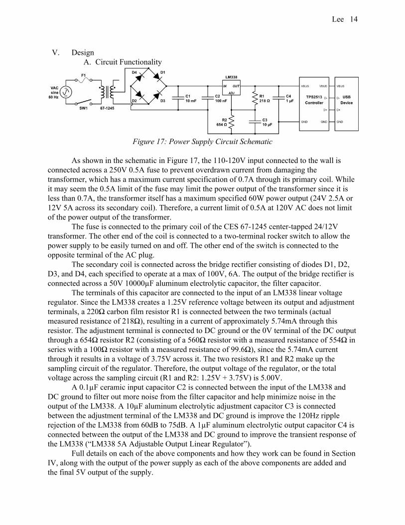
Figure 17: Power Supply Circuit Schematic
As shown in the schematic in Figure 17, the 110-120V input connected to the wall is
connected across a 250V 0.5A fuse to prevent overdrawn current from damaging the transformer, which has a maximum current specification of 0.7A through its primary coil. While it may seem the 0.5A limit of the fuse may limit the power output of the transformer since it is less than 0.7A, the transformer itself has a maximum specified 60W power output (24V 2.5A or 12V 5A across its secondary coil). Therefore, a current limit of 0.5A at 120V AC does not limit of the power output of the transformer.
The fuse is connected to the primary coil of the CES 67-1245 center-tapped 24/12V transformer. The other end of the coil is connected to a two-terminal rocker switch to allow the power supply to be easily turned on and off. The other end of the switch is connected to the opposite terminal of the AC plug.
The secondary coil is connected across the bridge rectifier consisting of diodes D1, D2, D3, and D4, each specified to operate at a max of 100V, 6A. The output of the bridge rectifier is connected across a 50V 10000µF aluminum electrolytic capacitor, the filter capacitor.
The terminals of this capacitor are connected to the input of an LM338 linear voltage regulator. Since the LM338 creates a 1.25V reference voltage between its output and adjustment terminals, a 220Ω carbon film resistor R1 is connected between the two terminals (actual measured resistance of 218Ω), resulting in a current of approximately 5.74mA through this resistor. The adjustment terminal is connected to DC ground or the 0V terminal of the DC output through a 654Ω resistor R2 (consisting of a 560Ω resistor with a measured resistance of 554Ω in series with a 100Ω resistor with a measured resistance of 99.6Ω), since the 5.74mA current through it results in a voltage of 3.75V across it. The two resistors R1 and R2 make up the sampling circuit of the regulator. Therefore, the output voltage of the regulator, or the total voltage across the sampling circuit (R1 and R2: 1.25V + 3.75V) is 5.00V.
A 0.1µF ceramic input capacitor C2 is connected between the input of the LM338 and DC ground to filter out more noise from the filter capacitor and help minimize noise in the output of the LM338. A 10µF aluminum electrolytic adjustment capacitor C3 is connected between the adjustment terminal of the LM338 and DC ground is improve the 120Hz ripple rejection of the LM338 from 60dB to 75dB. A 1µF aluminum electrolytic output capacitor C4 is connected between the output of the LM338 and DC ground to improve the transient response of the LM338 (“LM338 5A Adjustable Output Linear Regulator”).
Full details on each of the above components and how they work can be found in Section IV, along with the output of the power supply as each of the above components are added and the final 5V output of the supply.
Lee 15
The 5V DC output of the LM338 is connected to two TPS2513EVM-527 USB charging controller chip evaluation boards, each of which have two USB outputs. These chips detect what device is connected to the USB output and send it the appropriate data signal it requires to begin charging while also supply the 5V output to the device itself to charge it. These controllers are what allow the unit to charge any mobile USB device. A complete functional diagram of the internal circuitry of the TPS2513EVM-527 can be found in Section XI Appendix C (“TPS2513EVM-527 Texas Instruments”).
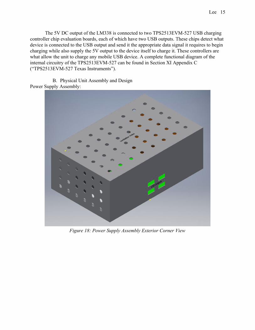
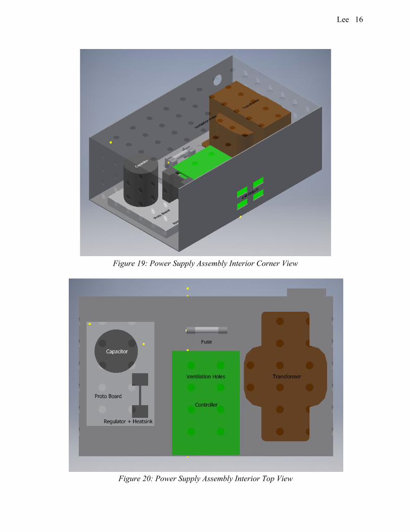
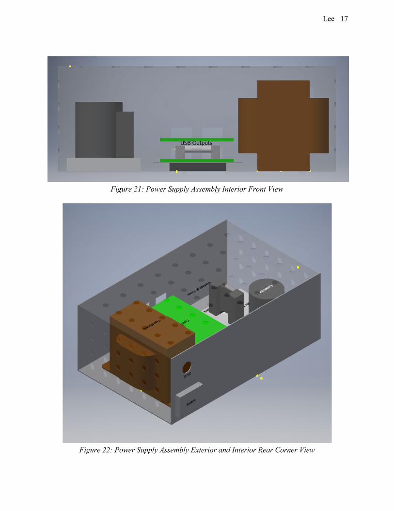
B. Physical Unit Assembly and Design Power Supply Assembly:
Figure 18: Power Supply Assembly Exterior Corner View
Lee 16
Figure 19: Power Supply Assembly Interior Corner View
Figure 20: Power Supply Assembly Interior Top View
Lee 17
Figure 21: Power Supply Assembly Interior Front View
Figure 22: Power Supply Assembly Exterior and Interior Rear Corner View
Lee 18
All of the circuit components are enclosed in a 8 x 5 x 3 in (internal dimensions) box of 18 gauge 6061-T4 aluminum sheet metal. The box is made of two U-shaped shells held together by screws for relatively easy internal assembly and maintenance. The front, bottom, and rear faces are connected as one shell and the top and side faces are connected as the other. All free electrical connections along the 120V AC line are made with 12 gauge insulated wire to sustain high power drawals. Wire is soldered directly to component terminals and all solder points are insulated with heat shrink tubing or electrical tape to minimize the risk of electrical shorts.
The AC input is at the rear of the box, near the top where it is close to the terminals of the primary coil of the transformer. The switch, fuse, and transformer are all near the rear of the power supply since they connect directly to the AC input. The physical ground from the AC input is connected directly to the metal box with solder and a bolt so that if any of the circuit components short or make contact with the box they will discharge directly through the box to an electrical ground, preventing other components from being damaged or outputs from damaging the user or any connected devices.
The end of the transformer with the secondary coil terminals faces the rectifier, proto board, and controller. Circuit boards are mounted with velcro to keep electrical connections insulated from the metal box. Since the large diodes of the rectifier do not fit in the proto board, the rectifier is mounted underneath the top surface of the box with electrical tape, and is connected with pressure crimp terminals, solder, and bolts. Small circuit elements such as diodes, resistors, and small capacitors are not shown in the assembly. A large TO-220 heatsink is attached to voltage regulator to keep it within its thermal limits even under excessive loads. Four output holes for USB outputs are on the front of the box with two TPS2513EVM-527 boards mounted with directly in front of them, each with their two USB output ports sticking through the holes.
Ventilation holes are cut in the sides and top faces of the box for passive air ventilation to keep the transformer and regulator from overheating the box. All components are spaced to provide significant airspace for passive air ventilation and to minimize the risk of short circuits by components making unintentional electrical contact, while minimizing the volume and footprint of the box. Fully dimensioned drawings of both the interior and exterior of the box can be found in Section XI Appendix D. VI. Next Steps
The next steps are to make the unit both more compact and efficient. The unit itself can become much more portable if custom printed circuit boards are incorporated into the design. With PCBs, all of the electronic components past the transformer can be connected to one small board. The rectifier would not need to be mounted separately and the TPS2513 controller chip could be mounted directly onto the PCB with surface mount solder, eliminating the need for separate evaluation unit boards. A smaller, perhaps toroidal, transformer would also make the unit much smaller as the transformer currently takes up most of volume.
To make the unit more efficient, the best remedy would be a switching regulator in place of the linear LM338 voltage regulator as most of the energy lost in the unit is due to the heat dissipated by the LM338. Both a lower output voltage transformer to reduce the voltage drop across the regulator and a switching regulator, with added digital controllers and chips to controller output current, would make the unit much more efficient.

Lee 19
VII. Results Since the current drawn by a mobile device is dependent on how charged its battery is (a
more depleted battery draws more current), the output power varied depending on the current supplied by the 5V output. The power output of the supply was measured with a multimeter to measure the output current drawn with a varying number of devices. The output power was calculated from this measurement using where I is output current and V is the 5V outputVP = I voltage. The input power drawn from the wall was measured with a P4 International P4400 Kill A Watt Electricity Meter and ranged from 5W to 11W for 1-2 devices (up to 44W for four devices). The output current was measured with either one or two loads of varying battery charges. Shown below is the output power vs. input power of the unit (the respective power drawals would multiply with more loads, though they may not be equal as different devices will draw different currents depending on their battery’s charge). As illustrated by the linear regression of Figure 23, the power supply operated with an average efficiency of 38.8%.
Figure 23: Power Output by Supply at Varying Input Power
The unit was also stress tested with four loads connected. The temperature of the LM338
voltage regulator was measured over time with an Etekcity Lasergrip 630 Digital Infrared Thermometer. In multiple hour-long stress tests, the temperature of the LM338 never exceeded 110 and stabilized at about 82, well below the LM338’s specified maximum operating temperature of 120 (“LM338 5A Adjustable Output Linear Regulator”).
VIII. Conclusion A stable 5V universal mobile USB power supply was successfully designed, constructed,
and stress tested. The supply charged up to four mobile devices simultaneously. Such modularity and universality allows for consumer electronics to become more open-source and less proprietary to specific manufacturers. Brand specific electronics and interfaces are not optimal for overall technological innovation as they undermine economic competition between manufacturers and strengthen monopolies. Steps to reduce competition reduce the investment

Lee 20
and competition that drive technology industries forward. If electronic devices can become more universal across wider platforms, ultimately technology will help more people, spread to more customers, and evolve more quickly. Electronic product design with universality over brand specificity in mind, as done with this power supply, would allow technology to become more widespread, modular, and and compatible with other devices. Ultimately, greater compatibility of electronic devices between different brands only allows for such technologies to accomplish more.
The power supply is limited by its large volume and weight and low efficiency. This could be further improved on as discussed in Section VI. The power supply’s low efficiency is primarily due to energy lost as heat in the LM338 regulator. The significant heat dissipation is due to the large (approximately 10V to 5V) voltage drop across the LM338 due to the input-output differential. This voltage drop was not eliminated to keep the LM338 operating well above its minimum 3V input-output differential. Energy losses also occur due to voltage drops and heat dissipation within the rectifier diodes and transformer coils, which have a small Ohmic resistance.
The measurements of the power supply’s input and output power were methodically limited. The input measurement was limited by the precision of the P4400 Kill A Watt Electricity Meter, which only measured power drawn to the nearest Watt. The output measurement was limited by the varying output current over time due to the changing battery charge of the connected charging device. The maximum value for both input power and output current were simultaneously recorded. IX. Acknowledgements
Thank you to Dr. James Dann for answering many questions about various electronics, providing insight and troubleshooting techniques into the many mind boggling problems that arose, and miraculously finding the perfect electronics online for the power supply.
Thank you to Mr. Brian Ward for assisting with the many physical design issues and teaching me how to use all of the appropriate tools to construct the unit.
Thank you to Paul Scherz for his informative book Practical Electronics of Inventors which provided a significant amount of the background information on various circuit components (much of which was used in this paper).
Thank you to Nikhil Singhal for holding loose wires and other electronics down without fear of getting burned so that they could be soldered when the helping hand failed to hold them close enough.
Thank you to Lauren Yang for watching Bob Ross’s “The Joy of Painting” on my phone to drain its battery for the output power tests.
Thank you to everyone who let me borrow their phone and charge it with the unit. Thank you to my trusty oscilloscope and multimeter which let me troubleshoot literally
everything in the circuit.
Lee 21
X. Works Cited
“Electricity 101.” Department of Energy, U.S. Department of Energy,
energy.gov/oe/information-center/educational-resources/electricity-101.
Harnden, John D., Jr. “Power Transmission.” Edison Tech Center, 2014,
www.edisontechcenter.org/Transmission.html.
Lantero, Allison. “The War of the Currents: AC vs. DC Power.” Department of Energy, U.S.
Department of Energy, energy.gov/articles/war-currents-ac-vs-dc-power.
“LM338 5A Adjustable Output Linear Regulator.” Texas Instruments, 2016,
www.ti.com/product/LM338.
“Magnetic Properties of Solids.” HyperPhysics, C.R. Nave,
hyperphysics.phy-astr.gsu.edu/hbase/Tables/magprop.html.
Scherz, Paul. Practical Electronics for Inventors. McGraw-Hill Companies, 2000.
Toich, Frank. “A Short History of the Evolved Power Supply.” Kepco, 2017,
www.kepcopower.com/newsevo.htm.
“TPS2513EVM-527 Texas Instruments.” DigiKey Electronics,
www.digikey.com/products/en/development-boards-kits-programmers/evaluation-and-de
monstration-boards-and-kits/787?k=TPS2513.
Lee 22
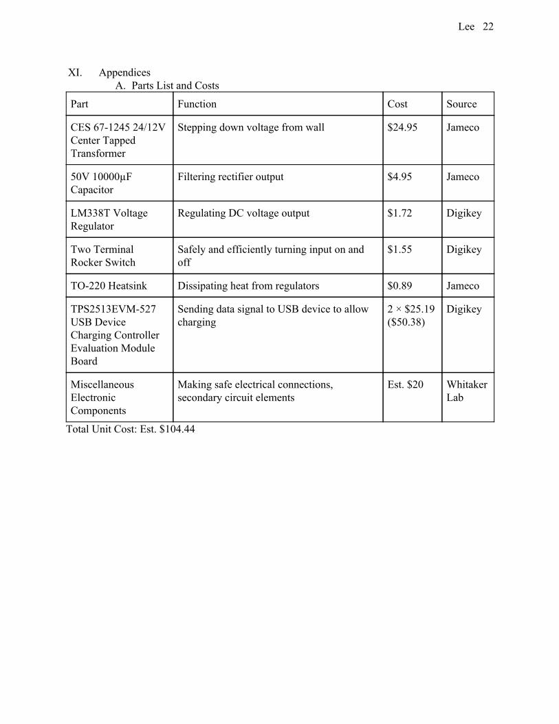
XI. Appendices A. Parts List and Costs
Part Function Cost Source
CES 67-1245 24/12V Center Tapped Transformer
Stepping down voltage from wall $24.95 Jameco
50V 10000µF Capacitor
Filtering rectifier output $4.95 Jameco
LM338T Voltage Regulator
Regulating DC voltage output $1.72 Digikey
Two Terminal Rocker Switch
Safely and efficiently turning input on and off
$1.55 Digikey
TO-220 Heatsink Dissipating heat from regulators $0.89 Jameco
TPS2513EVM-527 USB Device Charging Controller Evaluation Module Board
Sending data signal to USB device to allow charging
2 × $25.19 ($50.38)
Digikey
Miscellaneous Electronic Components
Making safe electrical connections, secondary circuit elements
Est. $20 Whitaker Lab
Total Unit Cost: Est. $104.44

Lee 23
B. LM338 Internal Functional Diagram
C. TPS2513EVM-27 Internal Functional Diagram
Lee 24
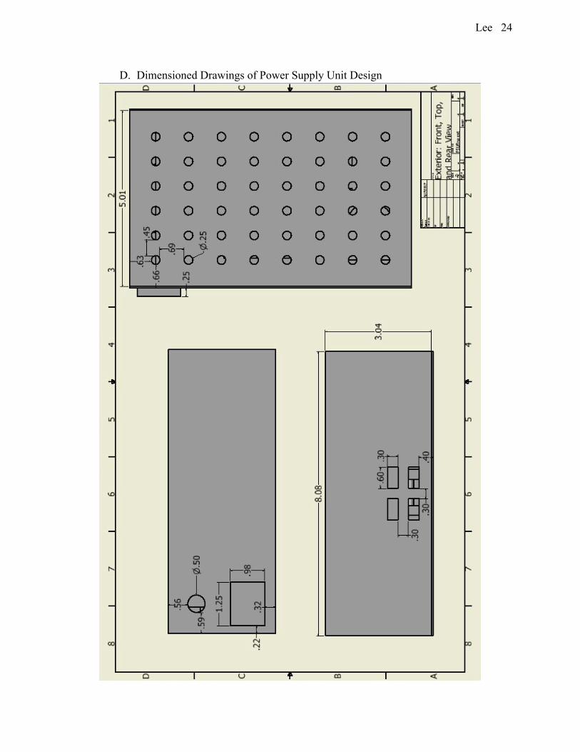
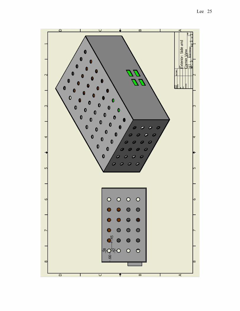
D. Dimensioned Drawings of Power Supply Unit Design
Lee 25
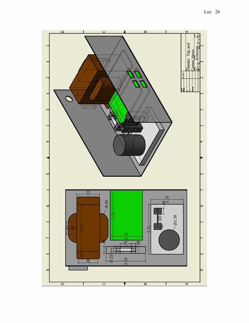
Lee 26
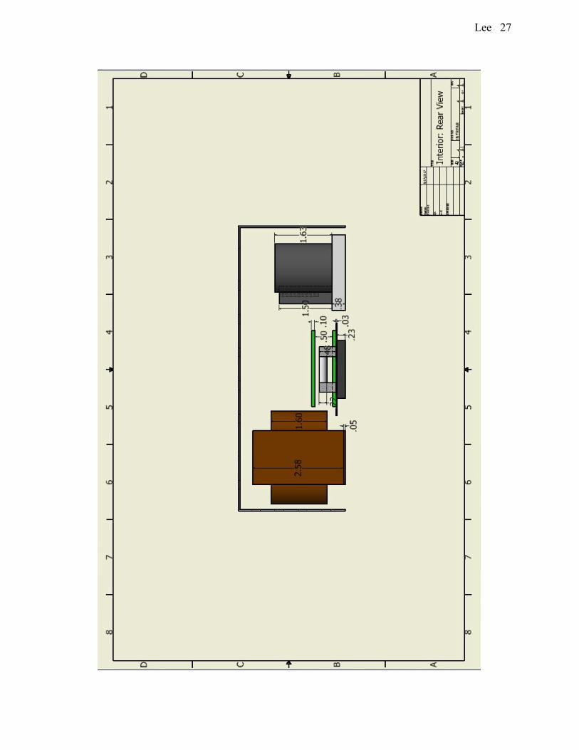
Lee 27