Embed Size (px)
Citation preview
DESIGNING OF COMBINATIONAL
LOGIC GATES IN CMOS
www.ppttopics.com
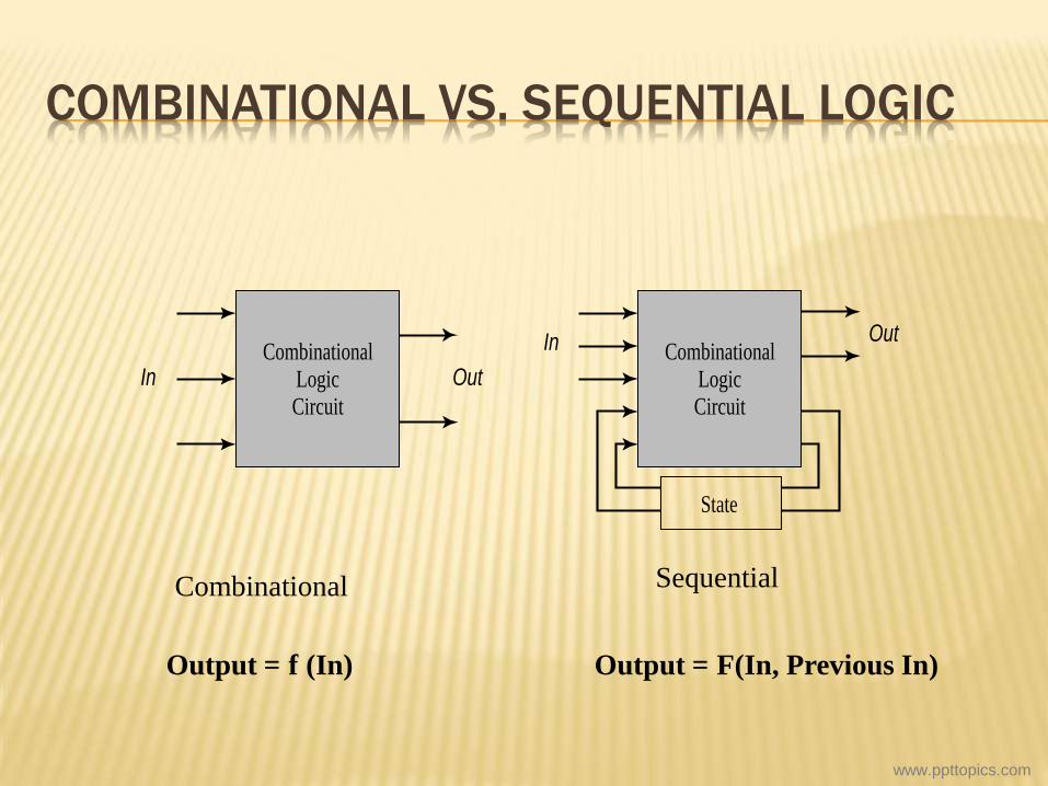
COMBINATIONAL VS. SEQUENTIAL LOGIC
CombinationalLogicCircuit
OutInCombinational
LogicCircuit
OutIn
State
Combinational Sequential
Output = f (In) Output = F(In, Previous In)
www.ppttopics.com
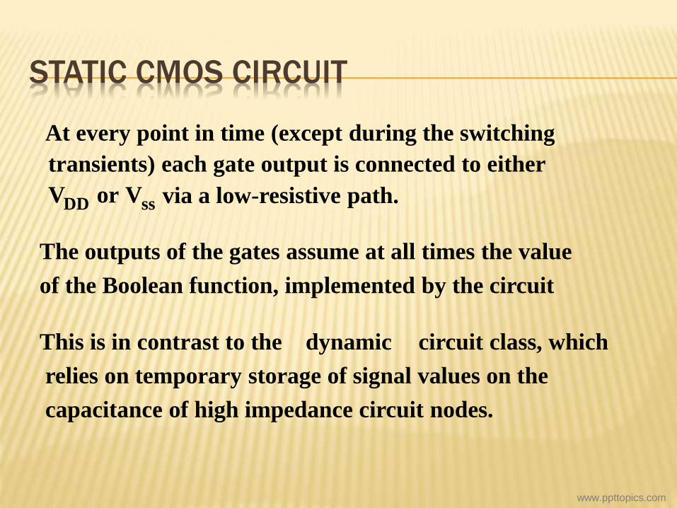
STATIC CMOS CIRCUIT
At every point in time (except during the switching
transients) each gate output is connected to either
V DD or V ss via a low-resistive path.
The outputs of the gates assume at all times the value
of the Boolean function, implemented by the circuit
This is in contrast to the dynamic circuit class, which
relies on temporary storage of signal values on the
capacitance of high impedance circuit nodes.
www.ppttopics.com
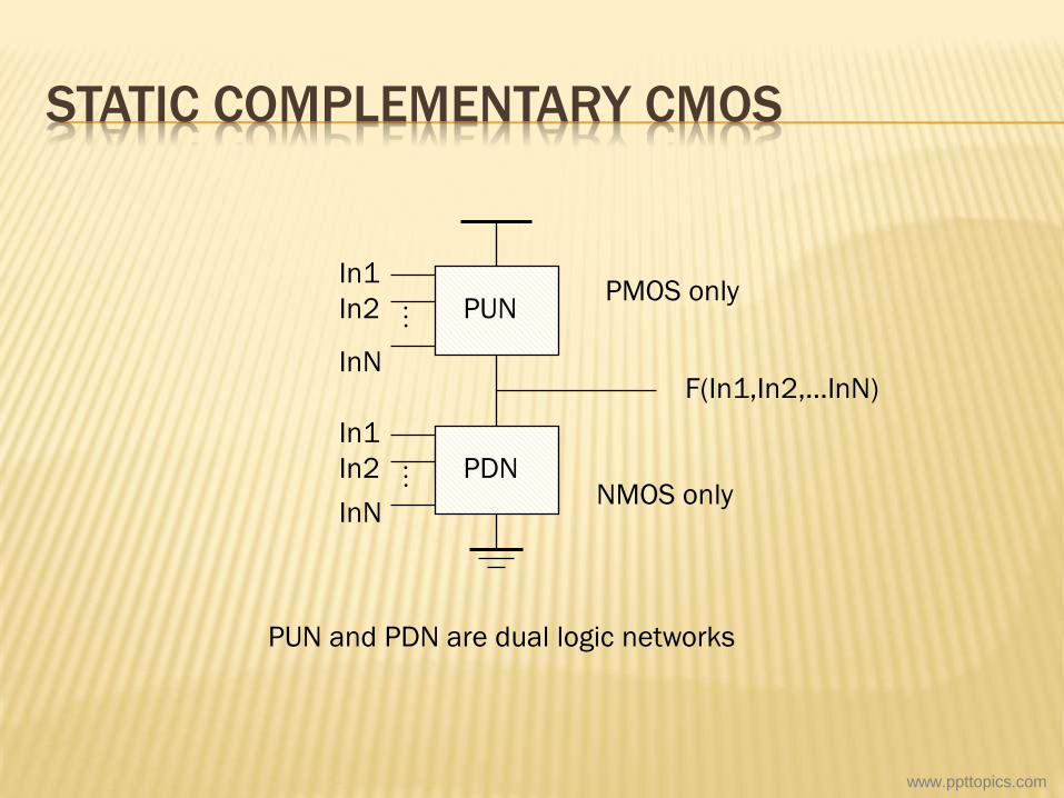
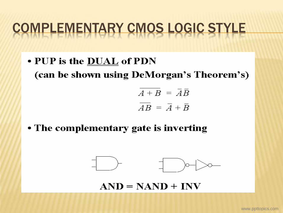
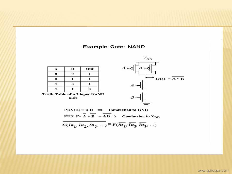
STATIC COMPLEMENTARY CMOS
F(In1,In2,…InN)
In1
In2
InN
In1
In2
InN
PUN
PDN
PMOS only
NMOS only
PUN and PDN are dual logic networks
www.ppttopics.com
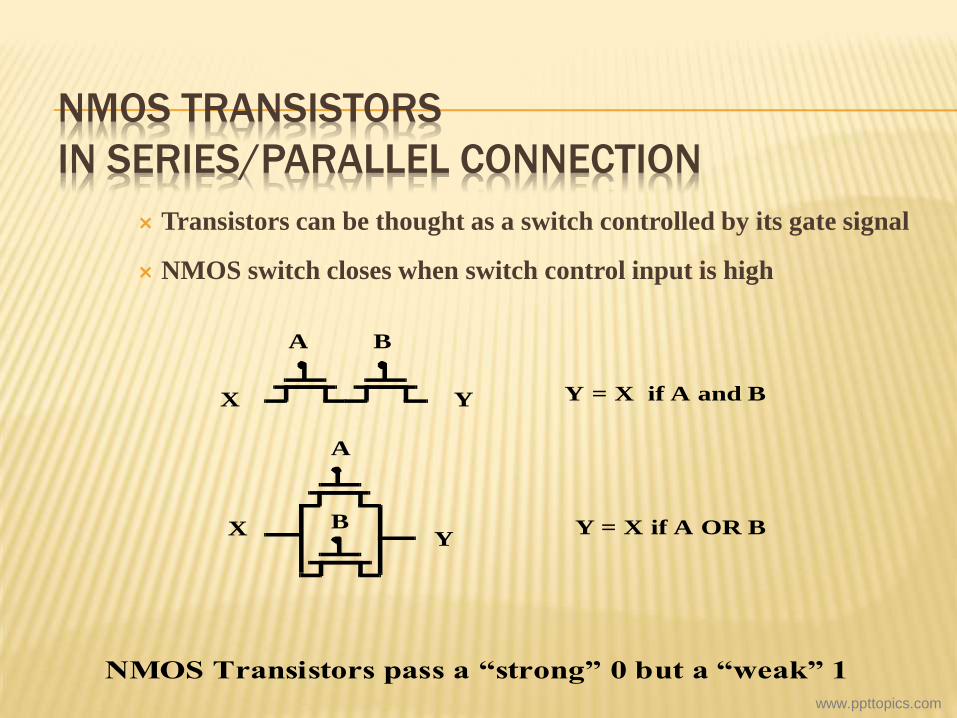
NMOS TRANSISTORS
IN SERIES/PARALLEL CONNECTION
Transistors can be thought as a switch controlled by its gate signal
NMOS switch closes when switch control input is high
X Y
A B
Y = X if A and B
XY
A
B Y = X if A OR B
NMOS Transistors pass a “strong” 0 but a “weak” 1
www.ppttopics.com
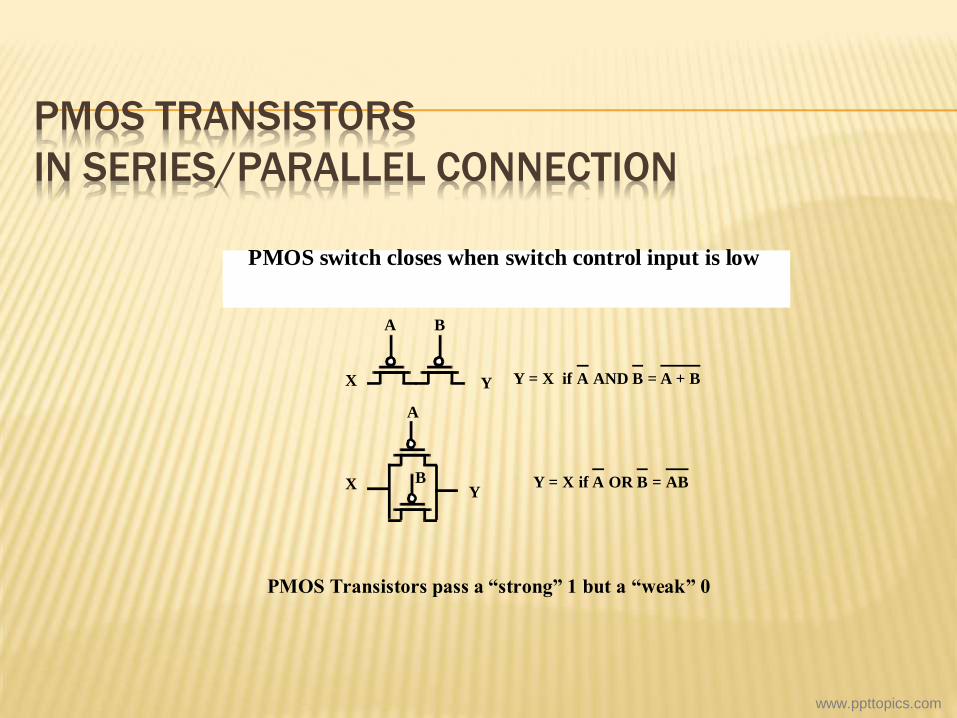
PMOS TRANSISTORS
IN SERIES/PARALLEL CONNECTION
X Y
A B
Y = X if A AND B = A + B
XY
A
B Y = X if A OR B = AB
PMOS Transistors pass a “strong” 1 but a “weak” 0
PMOS switch closes when switch control input is low
www.ppttopics.com
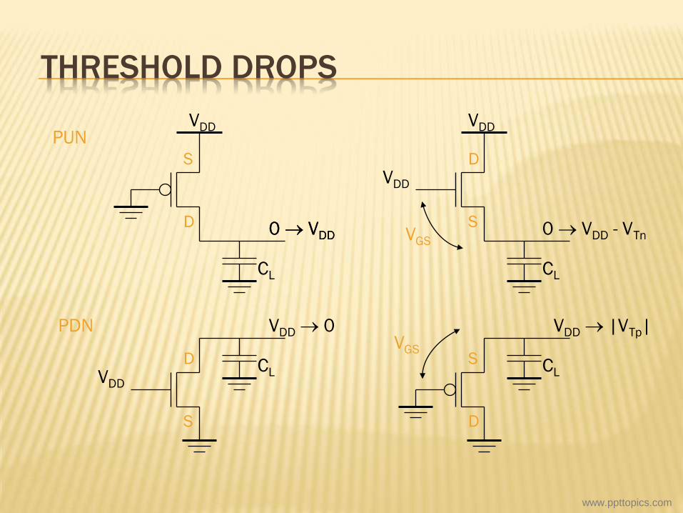
THRESHOLD DROPS
VDD 0 PDN
CL VDD CL
S
S D
D
VGS
0 VDD
PUN
0 VDD - VTn
VDD |VTp|
VDD
0 VDD
CL
S
D
CL
VDD
VDD
S
D
VGS
www.ppttopics.com
COMPLEMENTARY CMOS LOGIC STYLE
www.ppttopics.com
www.ppttopics.com
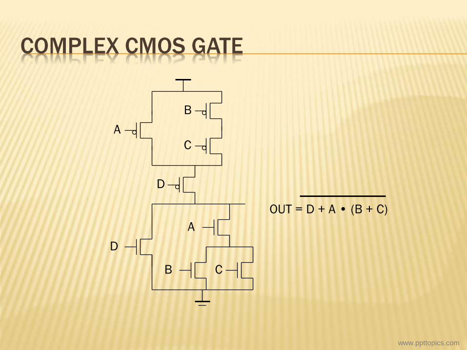
COMPLEX CMOS GATE
D
A
B C
D
A
B
C
OUT = D + A • (B + C)
www.ppttopics.com
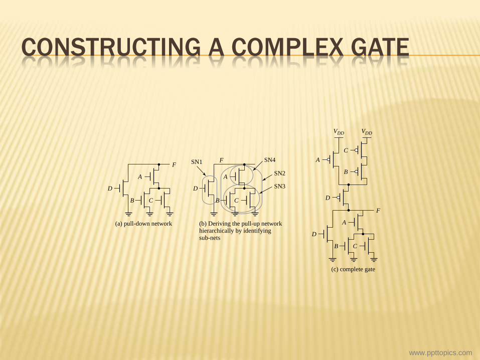
CONSTRUCTING A COMPLEX GATE
C
(a) pull-down network
SN1 SN4
SN2
SN3D
FF
A
DB
C
D
F
A
B
C
(b) Deriving the pull-up networkhierarchically by identifyingsub-nets
D
A
A
B
C
VDD VDD
B
(c) complete gate
www.ppttopics.com
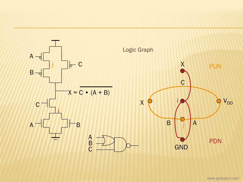
C
A B
X = C • (A + B)
B
A
C
i
j
A B C
Logic Graph
j
VDD X
X
i
GND
A B
C
PUN
PDN
www.ppttopics.com
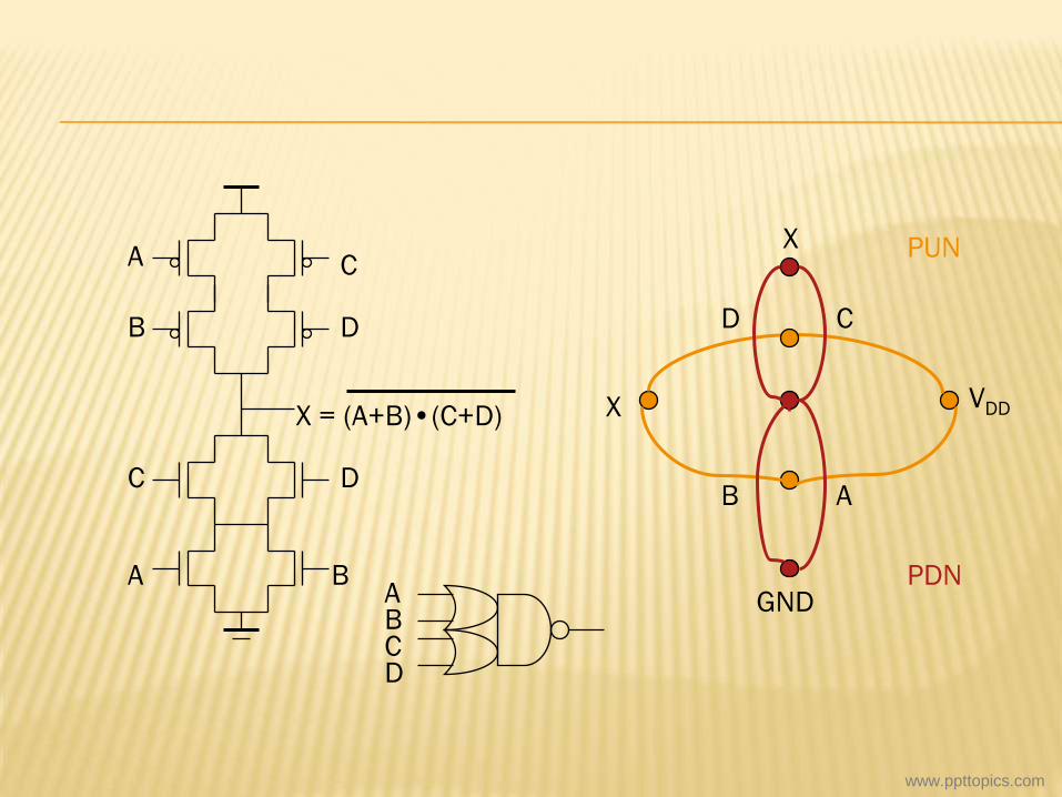
C
A B
X = (A+B)•(C+D)
B
A
D
VDD X
X
GND
A B
C
PUN
PDN
C
D
D
A B C D
www.ppttopics.com
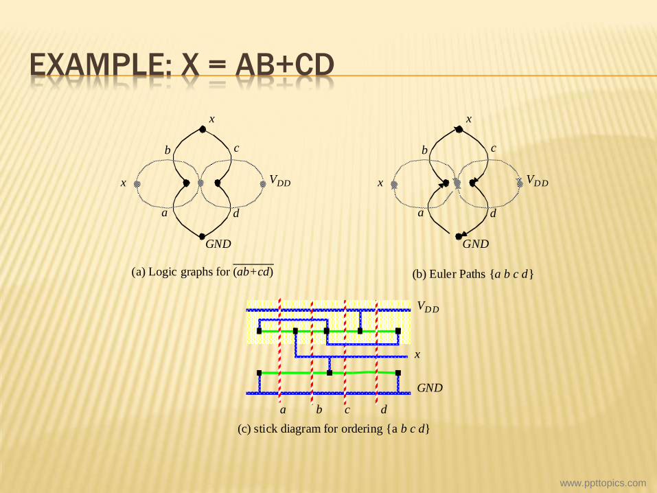
EXAMPLE: X = AB+CD
GND
x
a
b c
d
VDDx
GND
x
a
b c
d
VDDx
(a) Logic graphs for (ab+cd) (b) Euler Paths {a b c d}
a c d
x
VDD
GND
(c) stick diagram for ordering {a b c d}
b
www.ppttopics.com
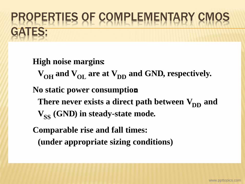
PROPERTIES OF COMPLEMENTARY CMOS
GATES:
High noise margins :
V OH and V OL are at V DD and GND , respectively.
No static power consumption :
There never exists a direct path between V DD and
V SS ( GND ) in steady-state mode .
Comparable rise and fall times:
(under appropriate sizing conditions)
www.ppttopics.com
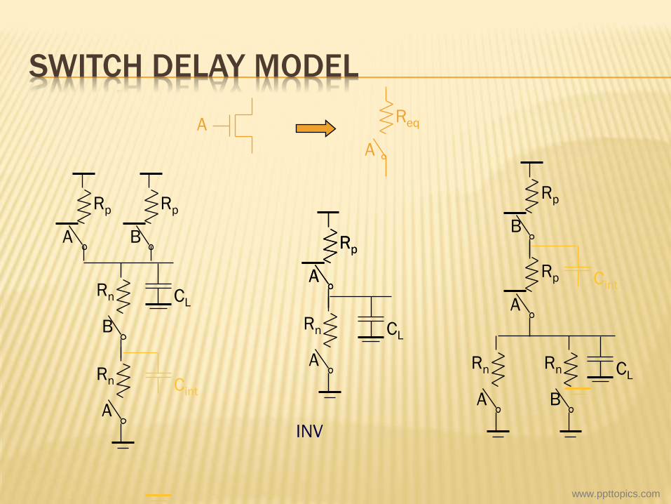
SWITCH DELAY MODEL
A
Req
A
Rp
A
Rp
A
Rn CL
A
CL
B
Rn
A
Rp
B
Rp
A
Rn Cint
B
Rp
A
Rp
A
Rn
B
Rn CL
Cint
INV
www.ppttopics.com
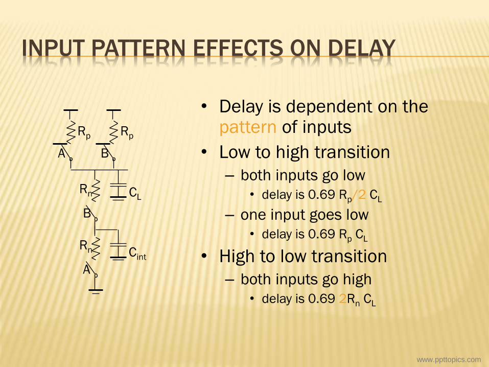
INPUT PATTERN EFFECTS ON DELAY
• Delay is dependent on the pattern of inputs
• Low to high transition
– both inputs go low
• delay is 0.69 Rp/2 CL
– one input goes low
• delay is 0.69 Rp CL
• High to low transition
– both inputs go high
• delay is 0.69 2Rn CL
CL
B
Rn
A
Rp
B
Rp
A
Rn Cint
www.ppttopics.com
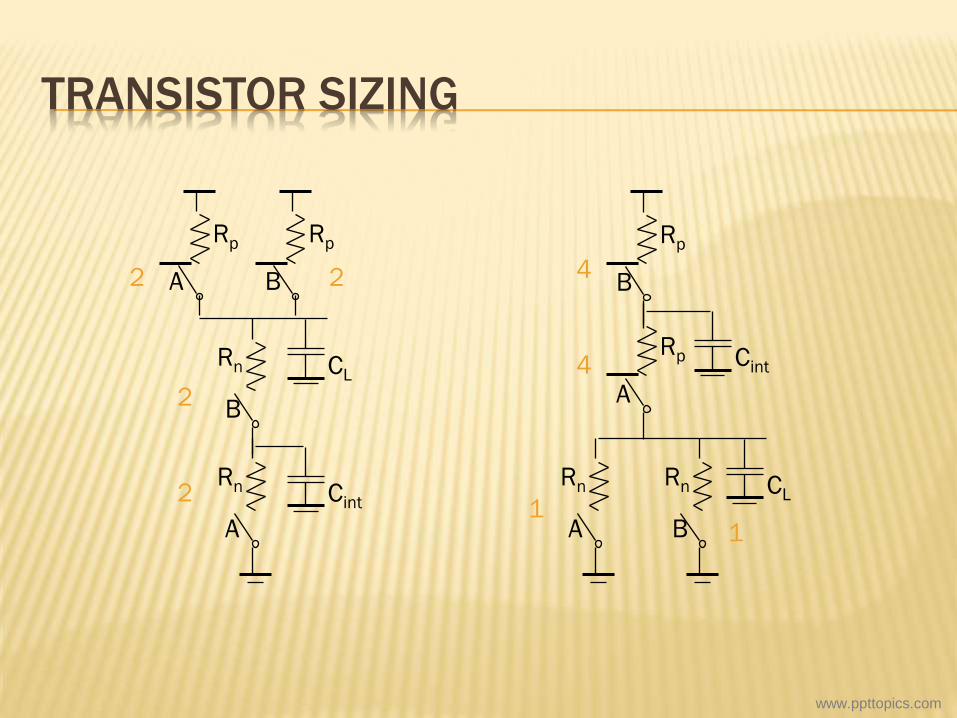
TRANSISTOR SIZING
CL
B
Rn
A
Rp
B
Rp
A
Rn Cint
B
Rp
A
Rp
A
Rn
B
Rn CL
Cint
2
2
2 2
1 1
4
4
www.ppttopics.com
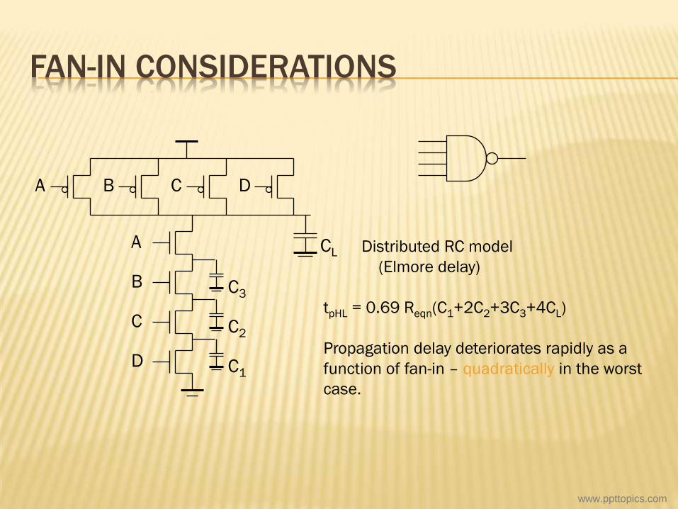
FAN-IN CONSIDERATIONS
D C B A
D
C
B
A CL
C3
C2
C1
Distributed RC model
(Elmore delay)
tpHL = 0.69 Reqn(C1+2C2+3C3+4CL)
Propagation delay deteriorates rapidly as a
function of fan-in – quadratically in the worst
case.
www.ppttopics.com
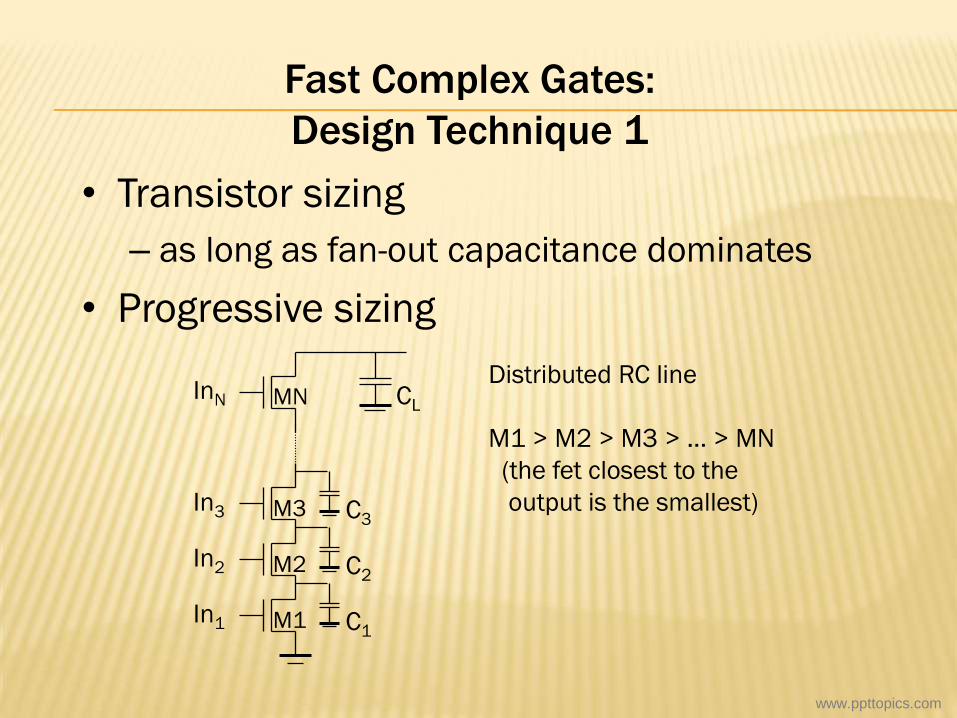
Fast Complex Gates:
Design Technique 1
• Transistor sizing
– as long as fan-out capacitance dominates
• Progressive sizing
InN CL
C3
C2
C1 In1
In2
In3
M1
M2
M3
MN
Distributed RC line
M1 > M2 > M3 > … > MN
(the fet closest to the
output is the smallest)
www.ppttopics.com
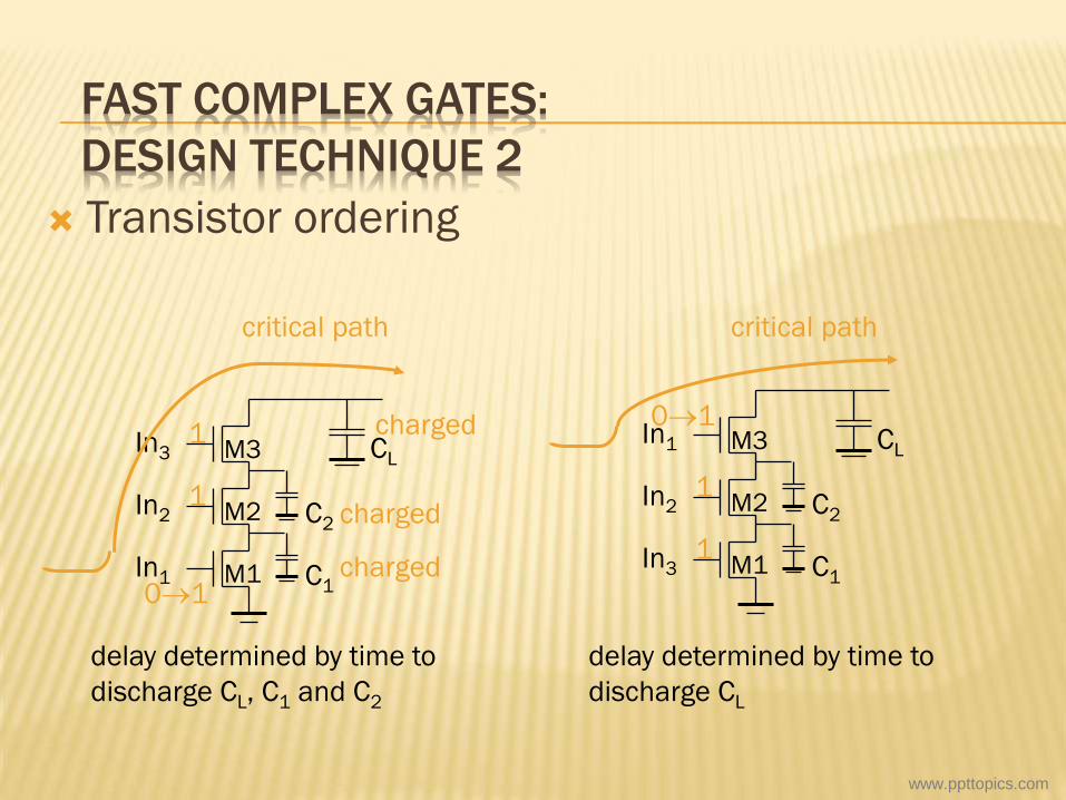
FAST COMPLEX GATES:
DESIGN TECHNIQUE 2
Transistor ordering
C2
C1 In1
In2
In3
M1
M2
M3 CL
C2
C1 In3
In2
In1
M1
M2
M3 CL
critical path critical path
charged 1
01 charged
charged 1
delay determined by time to
discharge CL, C1 and C2
delay determined by time to
discharge CL
1
1
01
www.ppttopics.com
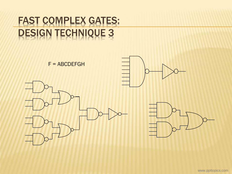
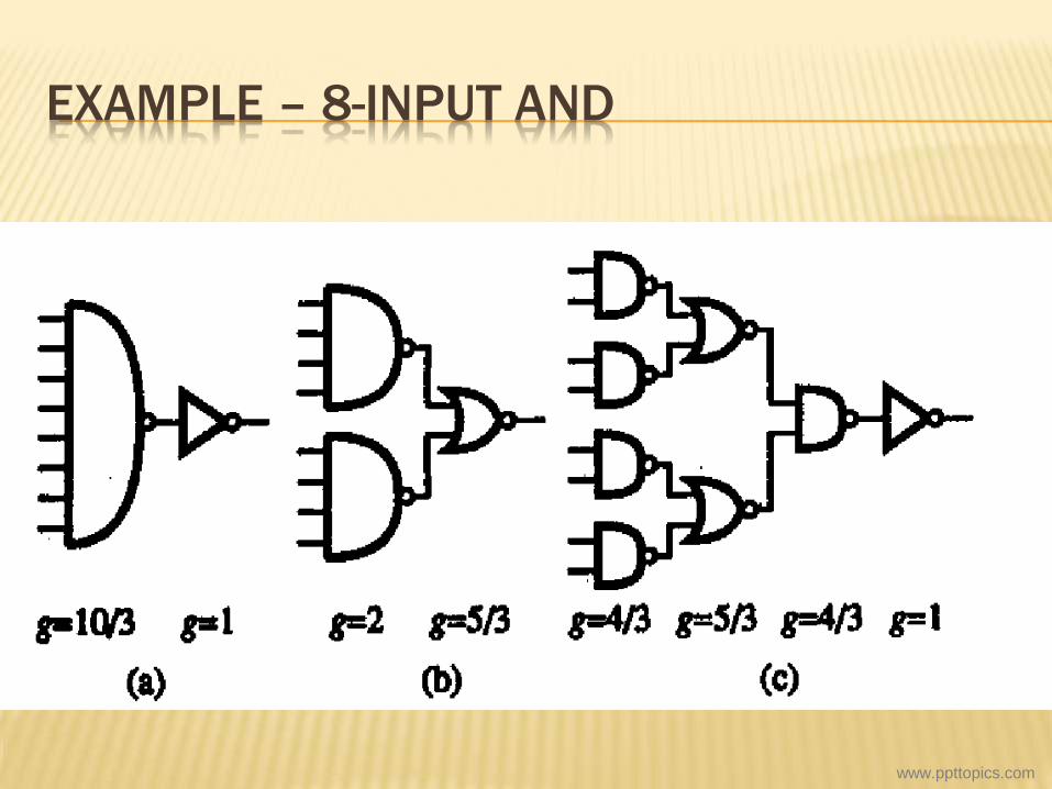
FAST COMPLEX GATES:
DESIGN TECHNIQUE 3
F = ABCDEFGH
www.ppttopics.com
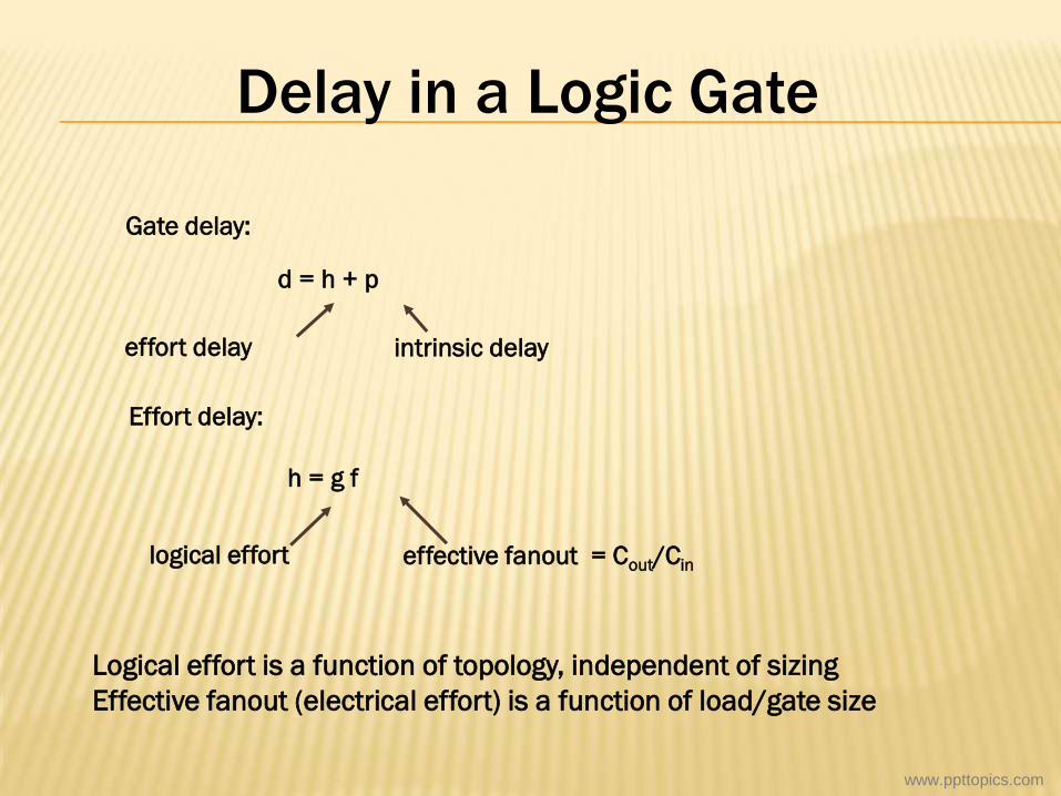
Delay in a Logic Gate
Gate delay:
d = h + p
effort delay intrinsic delay
Effort delay:
h = g f
logical effort effective fanout = Cout/Cin
Logical effort is a function of topology, independent of sizing
Effective fanout (electrical effort) is a function of load/gate size
www.ppttopics.com
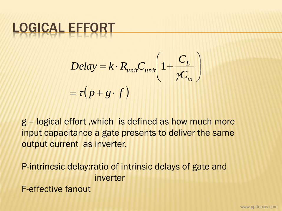
LOGICAL EFFORT
fgp
C
CCRkDelay
in
Lunitunit
1
g – logical effort ,which is defined as how much more
input capacitance a gate presents to deliver the same
output current as inverter.
P-intrincsic delay:ratio of intrinsic delays of gate and
inverter
F-effective fanout
www.ppttopics.com
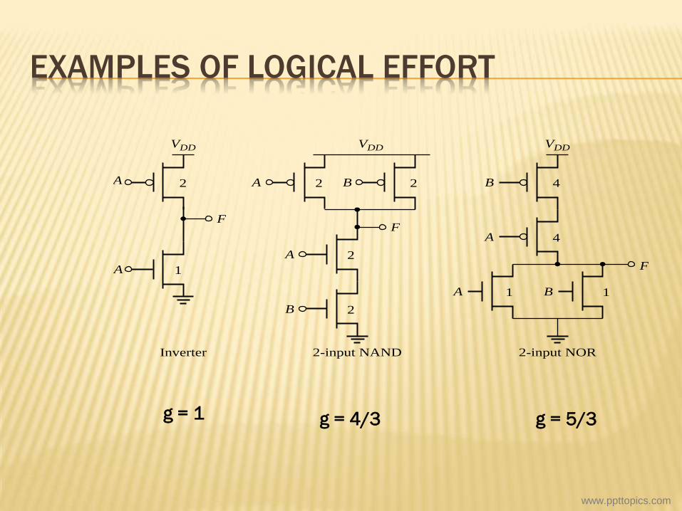
EXAMPLES OF LOGICAL EFFORT
B
A
A B
F
VDDVDD
A B
A
B
F
VDD
A
A
F
1
2 2 2
2
2
1 1
4
4
Inverter 2-input NAND 2-input NOR
g = 1 g = 4/3 g = 5/3
www.ppttopics.com
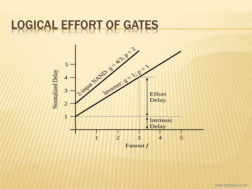
LOGICAL EFFORT OF GATES
Intrinsic�Delay
EffortDelay
1 2 3 4 5
Fanout f
1
2
3
4
5
Inverte
r:g =
1; p = 1
2-input N
AND: g = 4
/3; p =
2N
orm
aliz
ed D
elay
www.ppttopics.com
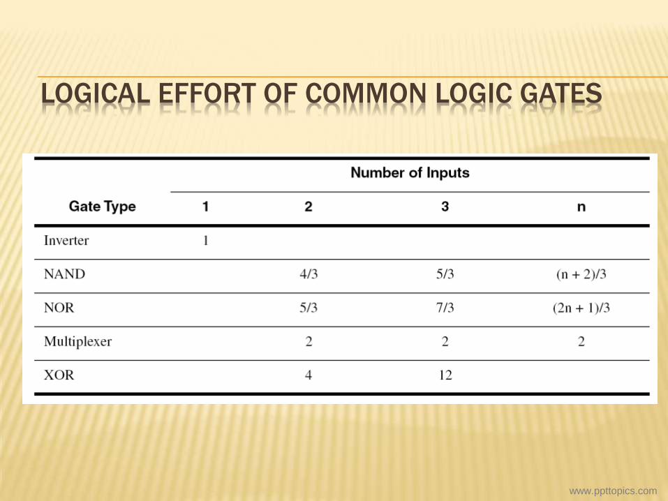
LOGICAL EFFORT OF COMMON LOGIC GATES
www.ppttopics.com
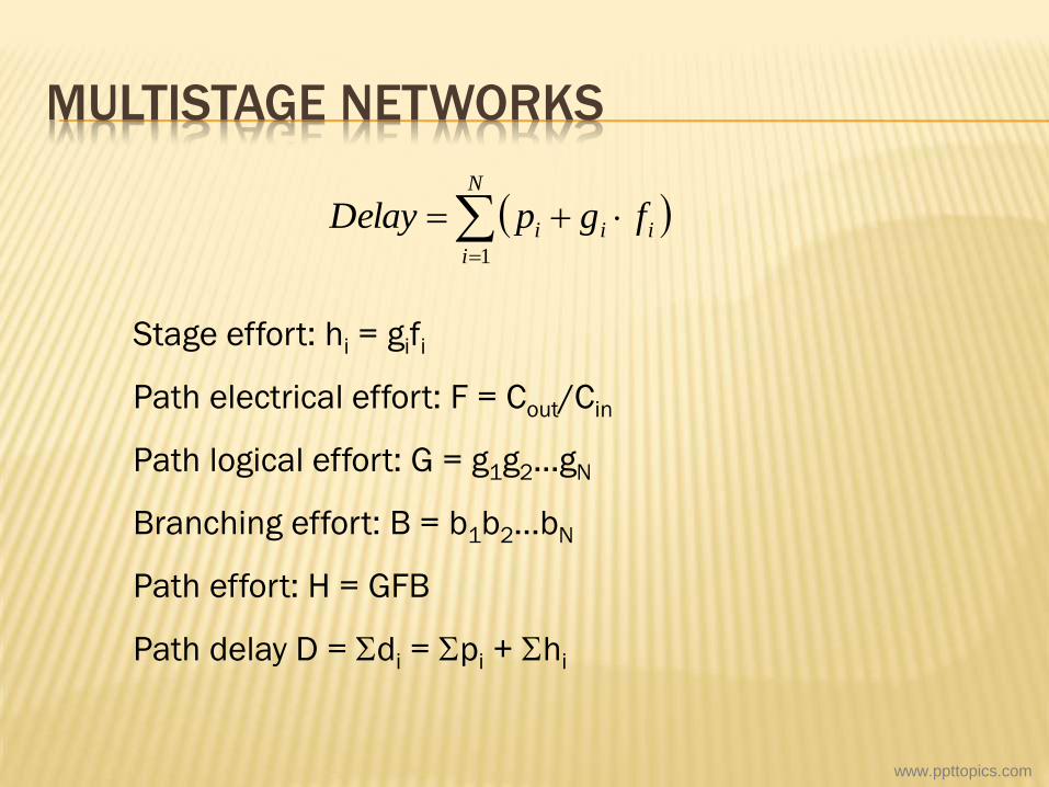
MULTISTAGE NETWORKS
N
i
iii fgpDelay1
Stage effort: hi = gifi
Path electrical effort: F = Cout/Cin
Path logical effort: G = g1g2…gN
Branching effort: B = b1b2…bN
Path effort: H = GFB
Path delay D = Sdi = Spi + Shi
www.ppttopics.com
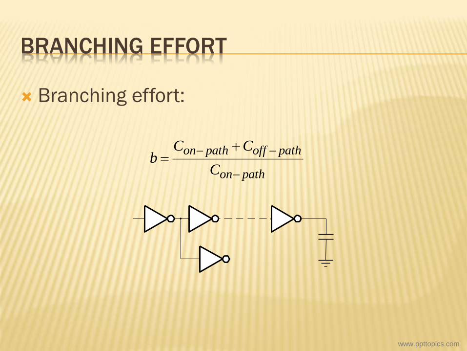
BRANCHING EFFORT
Branching effort:
pathon
pathoffpathon
C
CCb
www.ppttopics.com
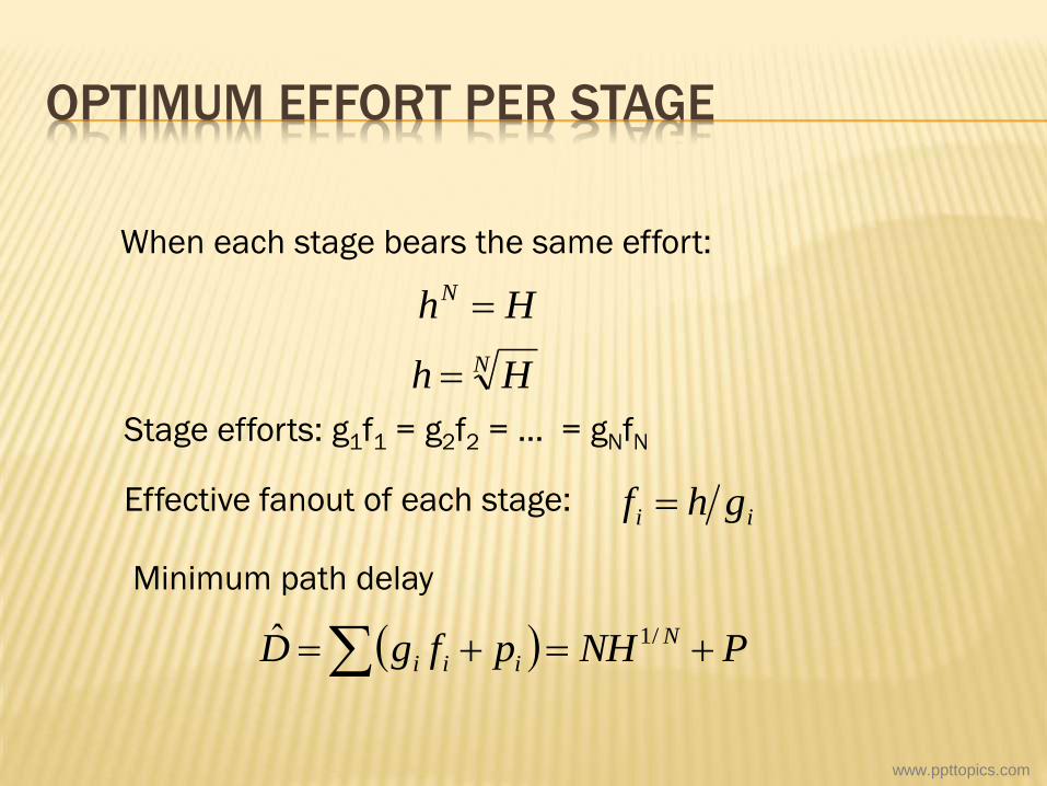
OPTIMUM EFFORT PER STAGE
HhN
When each stage bears the same effort:
N Hh
PNHpfgD N
iii /1ˆ
Minimum path delay
Effective fanout of each stage: ii ghf
Stage efforts: g1f1 = g2f2 = … = gNfN
www.ppttopics.com
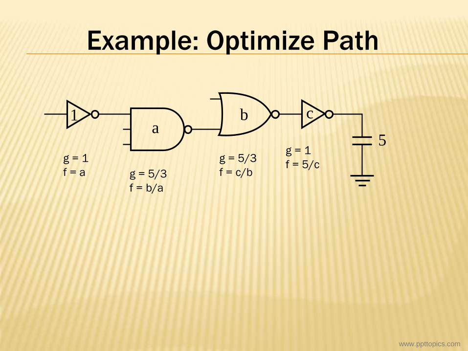
Example: Optimize Path
g = 1
f = a g = 5/3
f = b/a
g = 5/3
f = c/b
g = 1
f = 5/c
1a
b c
5
www.ppttopics.com
EXAMPLE – 8-INPUT AND
www.ppttopics.com
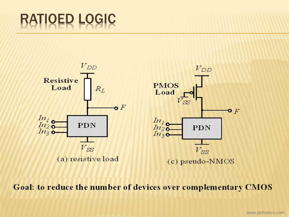
RATIOED LOGIC
www.ppttopics.com
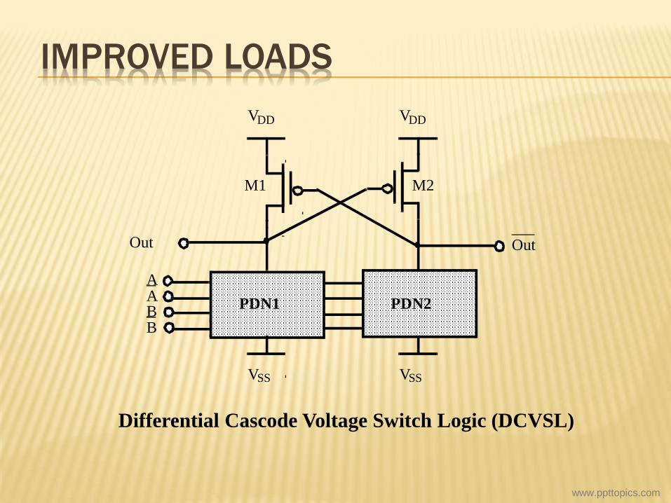
IMPROVED LOADS
V DD
V SS
PDN1
Out
V DD
V SS
PDN2
Out
A A B B
M1 M2
Differential Cascode Voltage Switch Logic (DCVSL)
www.ppttopics.com
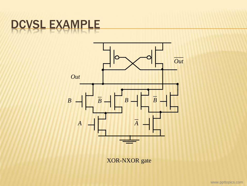
DCVSL EXAMPLE
B
A A
B B B
Out
Out
XOR-NXOR gate
www.ppttopics.com
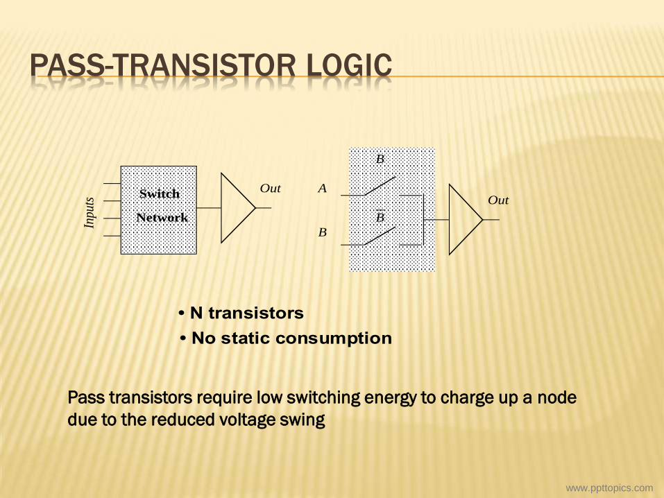
PASS-TRANSISTOR LOGIC In
puts
Switch
Network
OutOut
A
B
B
B
• N transistors
• No static consumption
Pass transistors require low switching energy to charge up a node
due to the reduced voltage swing
www.ppttopics.com
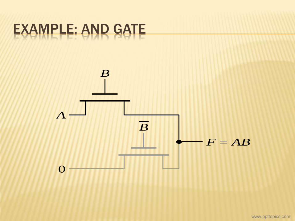
EXAMPLE: AND GATE
B
B
A
F = AB
0
www.ppttopics.com
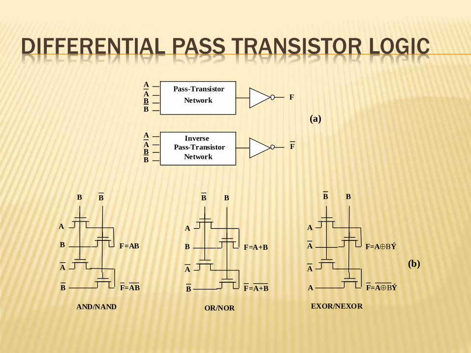
DIFFERENTIAL PASS TRANSISTOR LOGIC
A
B
A
B
B B B B
A
B
A
B
F=AB
F=AB
F=A+B
F=A+B
B B
A
A
A
A
F=AÝ
F=AÝ
OR/NOR EXOR/NEXORAND/NAND
F
F
Pass-Transistor
Network
Pass-Transistor
Network
A
ABB
A
ABB
Inverse
(a)
(b)
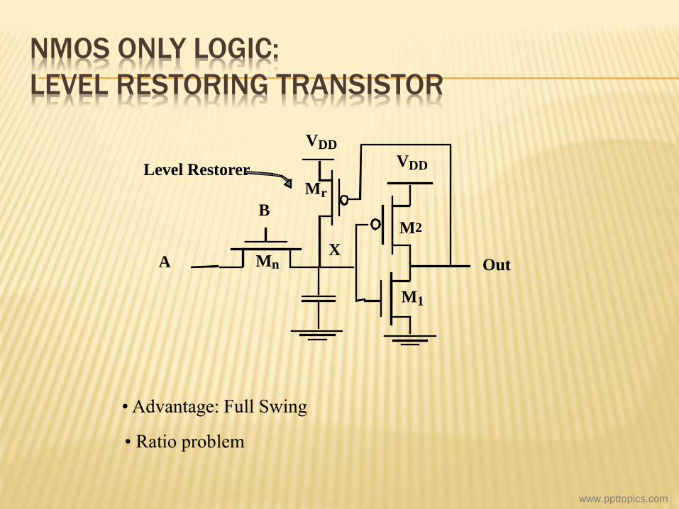
NMOS ONLY LOGIC:
LEVEL RESTORING TRANSISTOR
M 2
M 1
M n
M r
Out A
B
V DD
V DD Level Restorer
X
• Advantage: Full Swing
• Ratio problem
www.ppttopics.com
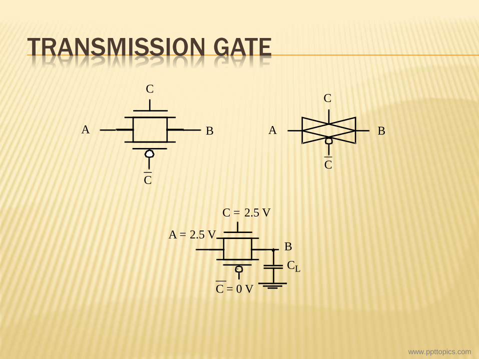
TRANSMISSION GATE
A B
C
C
A B
C
C
B
C L
C = 0 V
A = 2.5 V
C = 2.5 V
www.ppttopics.com
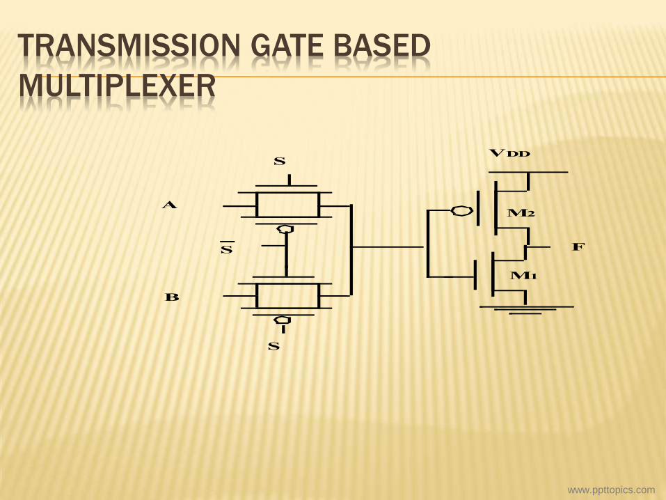
TRANSMISSION GATE BASED
MULTIPLEXER
AM2
M1
B
S
S
S F
VDD
www.ppttopics.com
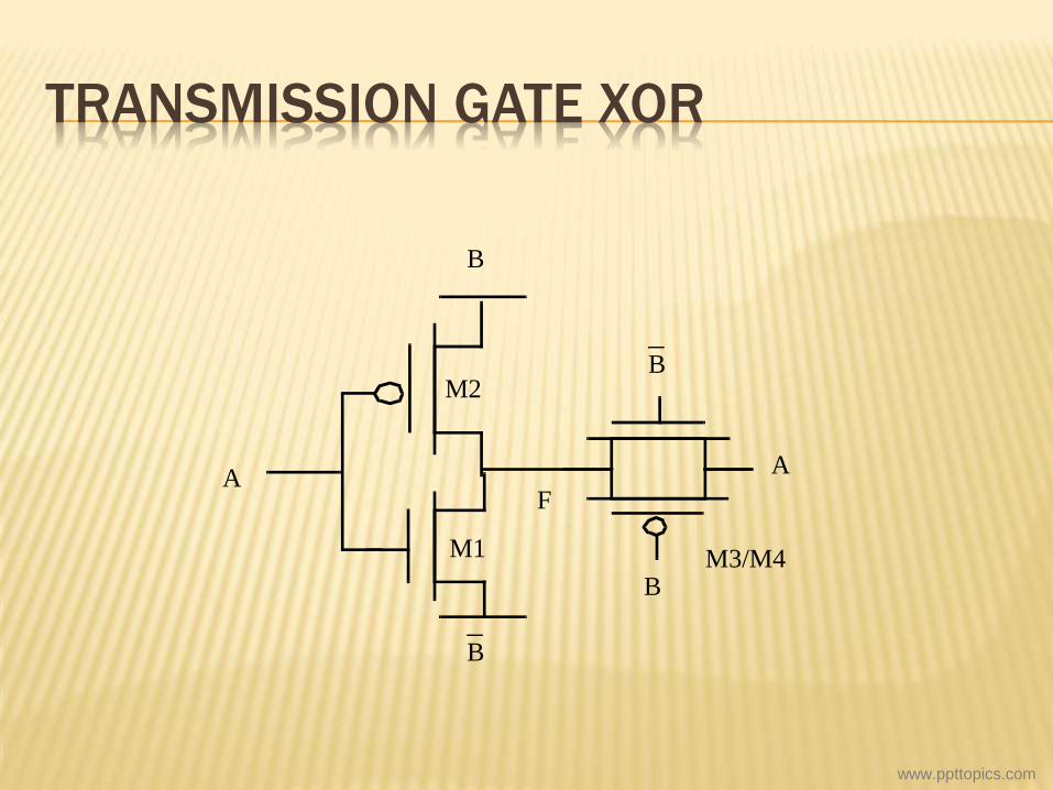
TRANSMISSION GATE XOR
A
B
F
B
A
B
B
M1
M2
M3/M4
www.ppttopics.com
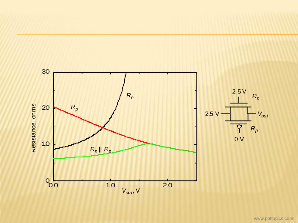
Vout
0 V
2.5 V
2.5 VRn
Rp
0.0 1.0 2.00
10
20
30
Vout, V
Resis
tance
, oh
ms
Rn
Rp
Rn || Rp
www.ppttopics.com
DELAY IN TRANSMISSION GATE NETWORKS
V 1 V i-1
C
2.5 2.5
0 0
V i V i+1
C C
2.5
0
V n-1 V n
C C
2.5
0
In
V 1 V i V i+1
C
V n-1 V n
C C
In
R eq R eq R eq R eq
C C
(a)
(b)
C
R eq R eq
C C
R eq
C C
R eq R eq
C C
R eq
C
In
m
(c)
www.ppttopics.com
www.ppttopics.com
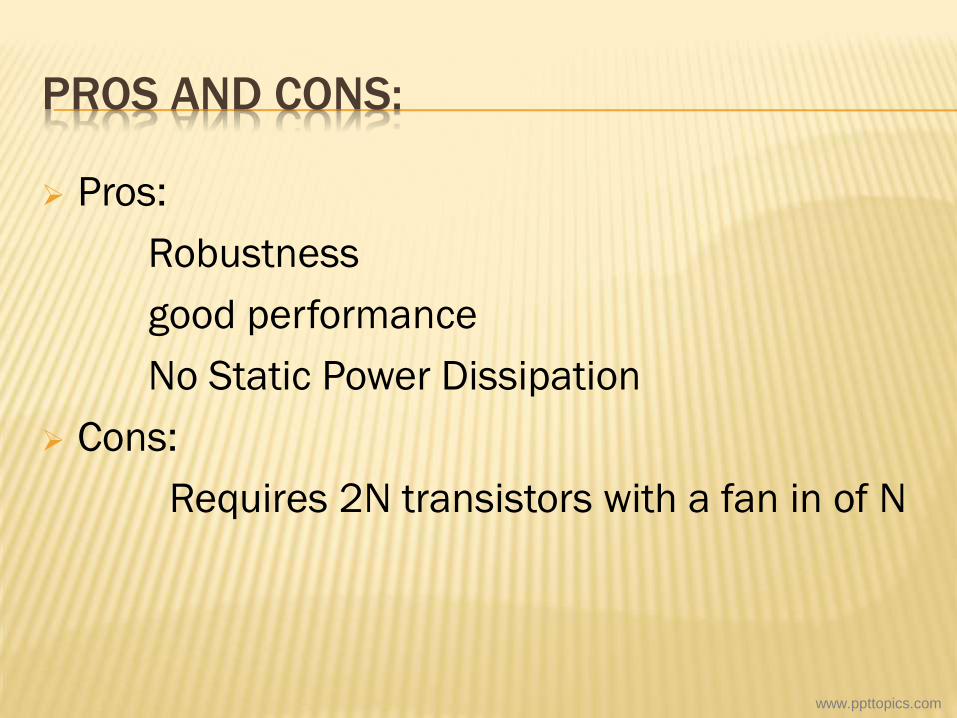
PROS AND CONS:
Pros:
Robustness
good performance
No Static Power Dissipation
Cons:
Requires 2N transistors with a fan in of N
www.ppttopics.com
CONCLUSION:
Static CMOS circuits can be used for devices
that have no extreme area,complexity or speed
constraints
www.ppttopics.com
REFERENCES:
1.DIGITAL INTEGRATED CIRCUTS BY
JAN RABAEY,
ANANTHA CHANDRAKASAN,
BORIVOJE NIKOLIC
2.http://bwrc.eecs.berkeley.edu/ICbook
www.ppttopics.com

THANK U
www.ppttopics.com