Embed Size (px)
Citation preview
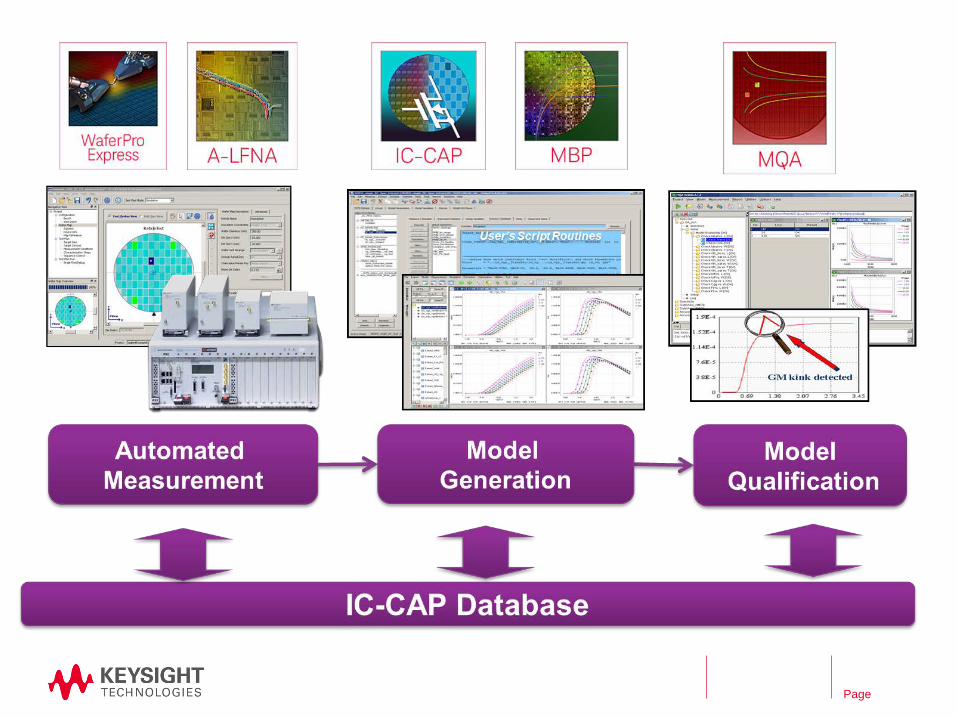
Device Modeling Turn-key Solutions from Measurement to Modeling and Quality Assurance
CHEN, JasonApplication EngineerKeysight Technologies
Oct. 18, 2016
Page
Page
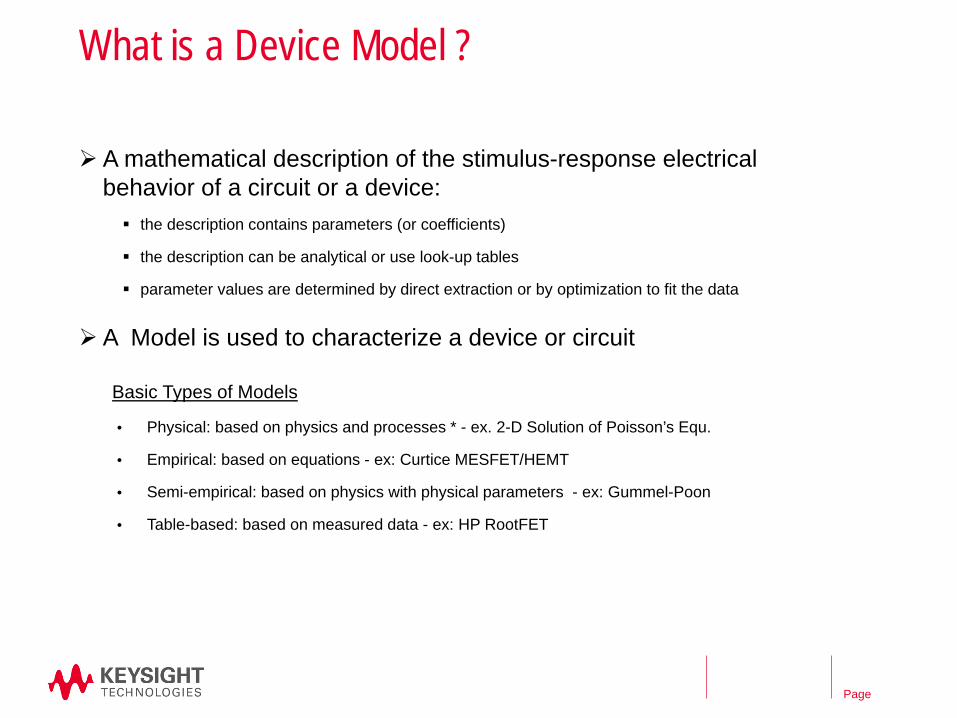
What is a Device Model ?
A mathematical description of the stimulus-response electrical behavior of a circuit or a device: the description contains parameters (or coefficients)
the description can be analytical or use look-up tables
parameter values are determined by direct extraction or by optimization to fit the data
A Model is used to characterize a device or circuit
Basic Types of Models
• Physical: based on physics and processes * - ex. 2-D Solution of Poisson’s Equ.
• Empirical: based on equations - ex: Curtice MESFET/HEMT
• Semi-empirical: based on physics with physical parameters - ex: Gummel-Poon
• Table-based: based on measured data - ex: HP RootFET
Page
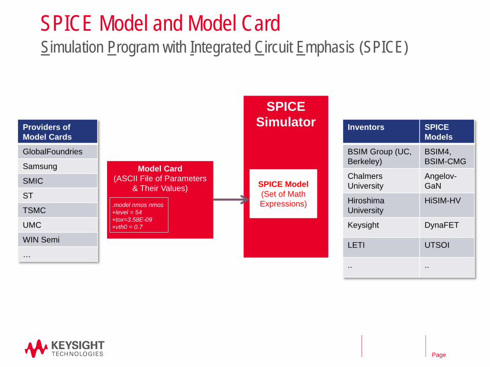
SPICE Model and Model CardSimulation Program with Integrated Circuit Emphasis (SPICE)
SPICE Simulator
SPICE Model(Set of Math Expressions)
Model Card(ASCII File of Parameters
& Their Values)
.model nmos nmos+level = 54 +tox=3.58E-09 +vth0 = 0.7
Providers of Model Cards
GlobalFoundries
Samsung
SMIC
ST
TSMC
UMC
WIN Semi
…
Inventors SPICE Models
BSIM Group (UC, Berkeley)
BSIM4, BSIM-CMG
Chalmers University
Angelov-GaN
Hiroshima University
HiSIM-HV
Keysight DynaFET
LETI UTSOI
.. ..
Page
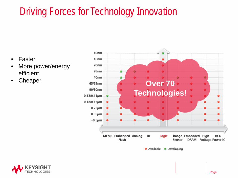
Driving Forces for Technology Innovation
Over 70 Technologies!
• Faster• More power/energy
efficient• Cheaper
Page
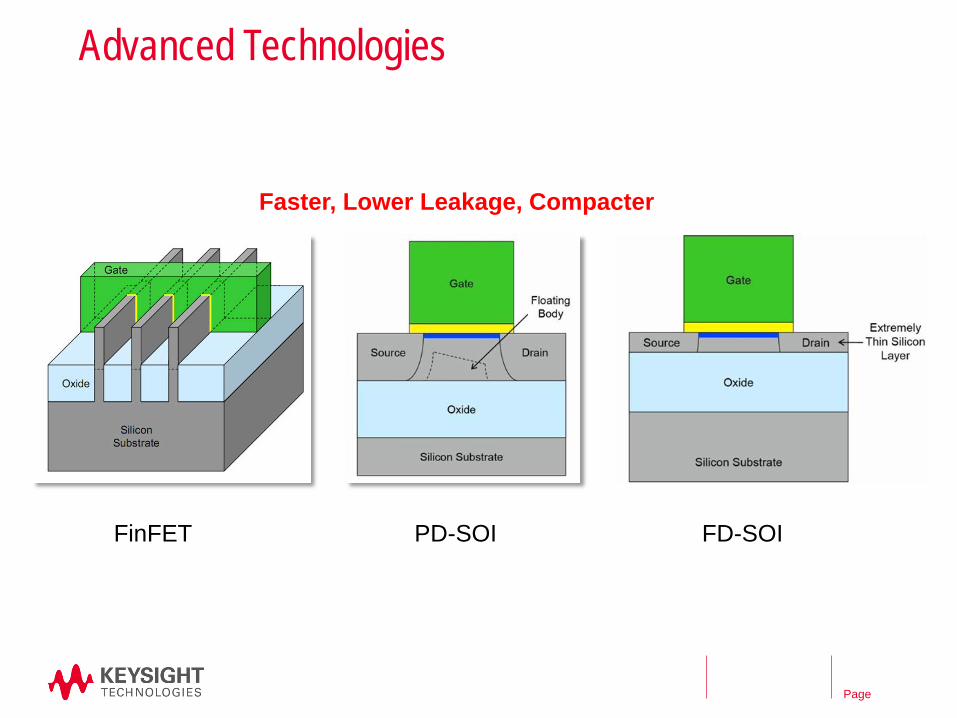
Advanced Technologies
FinFET PD-SOI FD-SOI
Faster, Lower Leakage, Compacter
Page
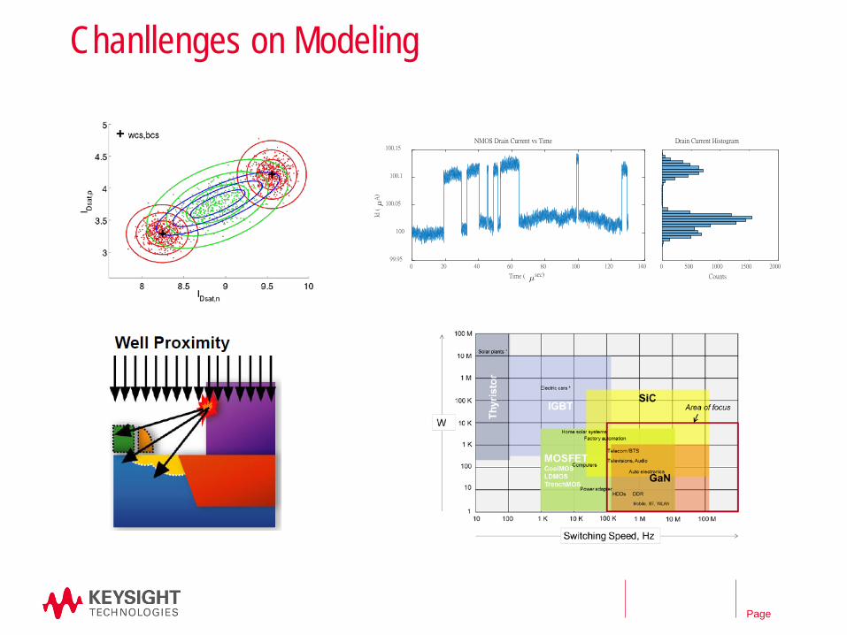
Chanllenges on Modeling
Time ( sec)
0 20 40 60 80 100 120 140
Id (
A)
99.95
100
100.05
100.1
100.15NMOS Drain Current vs Time
Counts
0 500 1000 1500 2000
Drain Current Histogram
Page
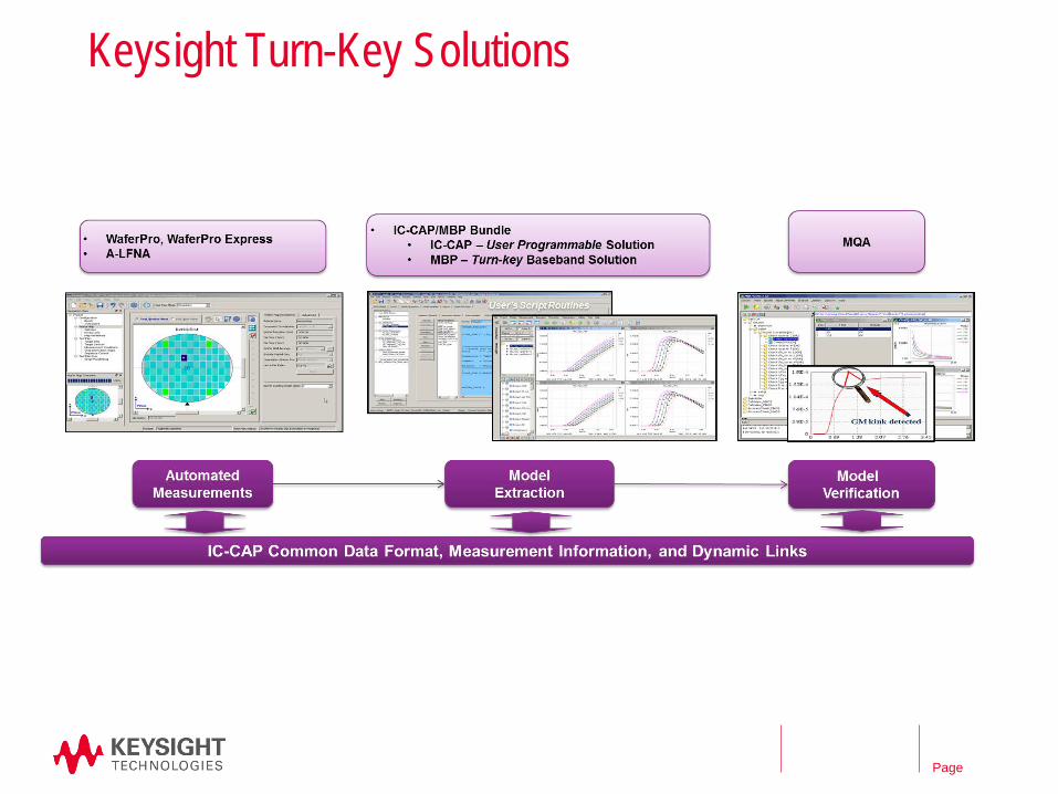
Keysight Turn-Key Solutions
Page
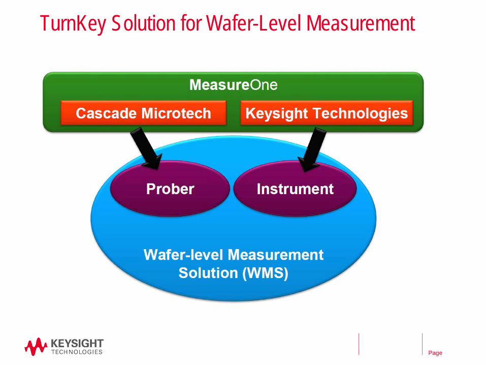
TurnKey Solution for Wafer-Level Measurement
Page
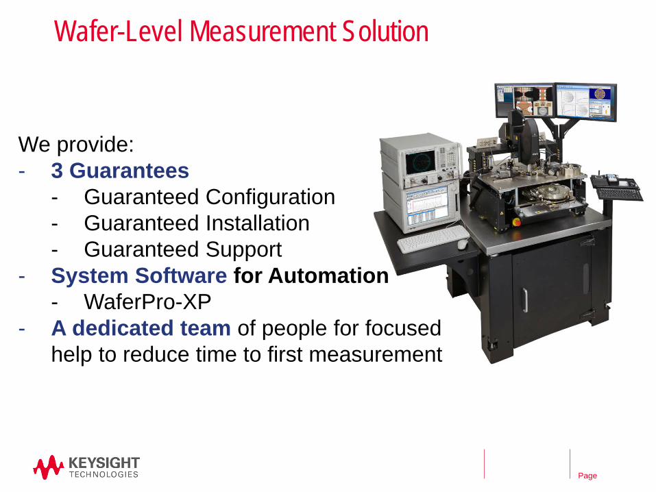
Wafer-Level Measurement Solution
We provide:- 3 Guarantees
- Guaranteed Configuration- Guaranteed Installation- Guaranteed Support
- System Software for Automation- WaferPro-XP
- A dedicated team of people for focused help to reduce time to first measurement
Page
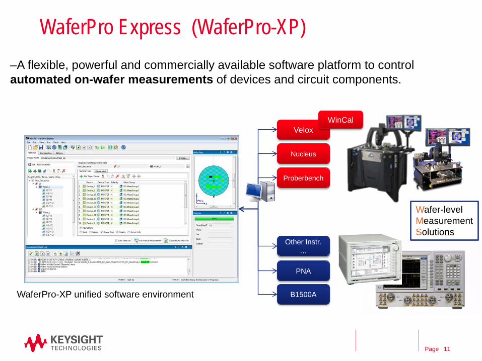
WaferPro Express (WaferPro-XP)–A flexible, powerful and commercially available software platform to control automated on-wafer measurements of devices and circuit components.
Nucleus
Other Instr. …
PNA
Velox
Proberbench
B1500A
Wafer-levelMeasurementSolutions
WinCal
WaferPro-XP unified software environment
11
Page
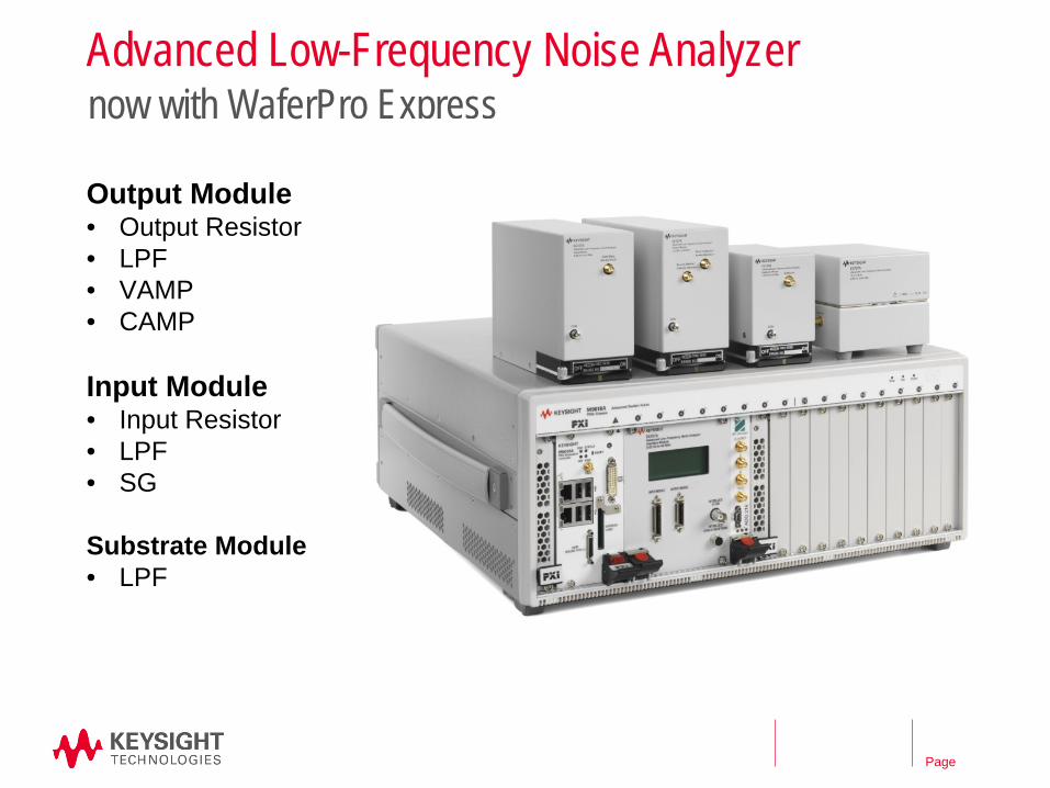
Advanced Low-Frequency Noise Analyzernow with WaferPro Express
Output Module• Output Resistor• LPF• VAMP• CAMP
Input Module• Input Resistor• LPF• SG
Substrate Module• LPF
Page
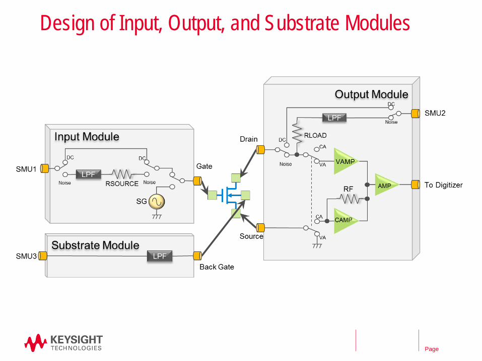
Design of Input, Output, and Substrate Modules
Page
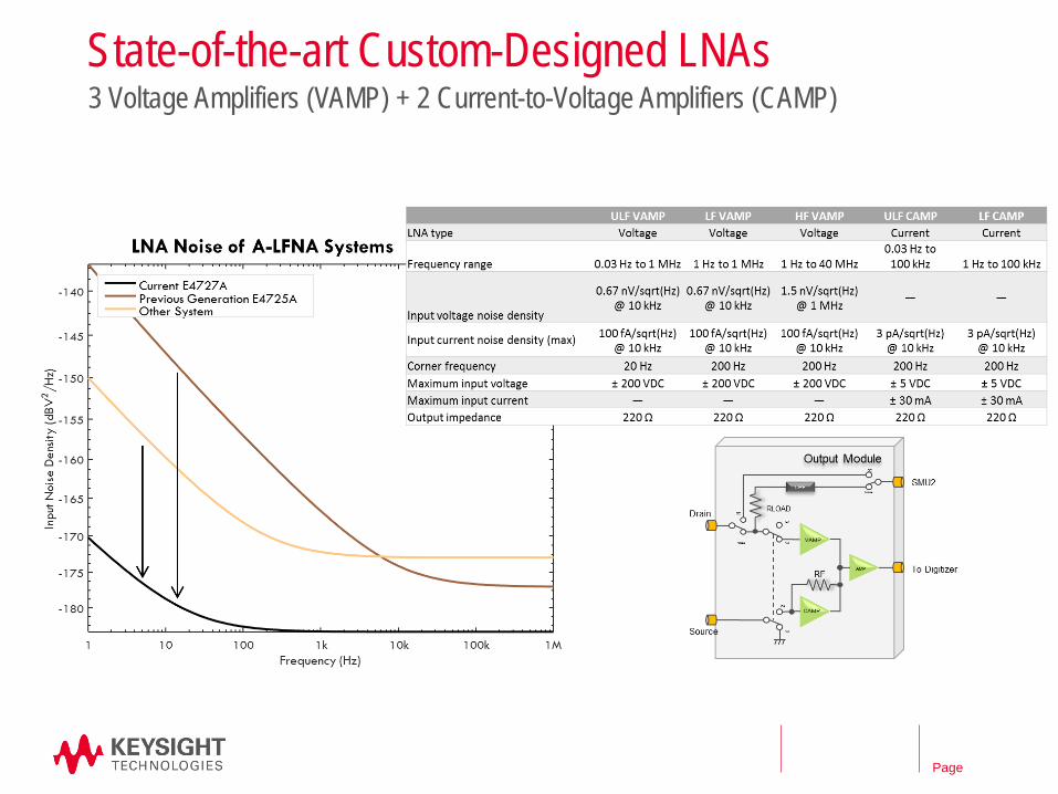
State-of-the-art Custom-Designed LNAs3 Voltage Amplifiers (VAMP) + 2 Current-to-Voltage Amplifiers (CAMP)
Page
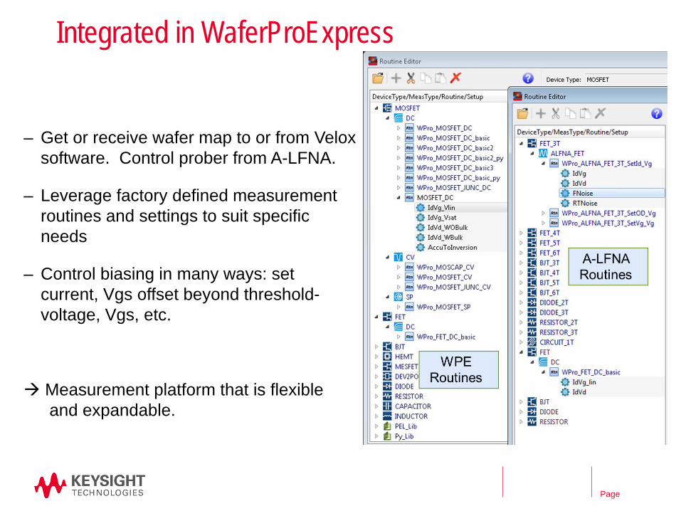
Integrated in WaferProExpress
– Get or receive wafer map to or from Velox software. Control prober from A-LFNA.
– Leverage factory defined measurement routines and settings to suit specific needs
– Control biasing in many ways: set current, Vgs offset beyond threshold-voltage, Vgs, etc.
Measurement platform that is flexible and expandable.
Page
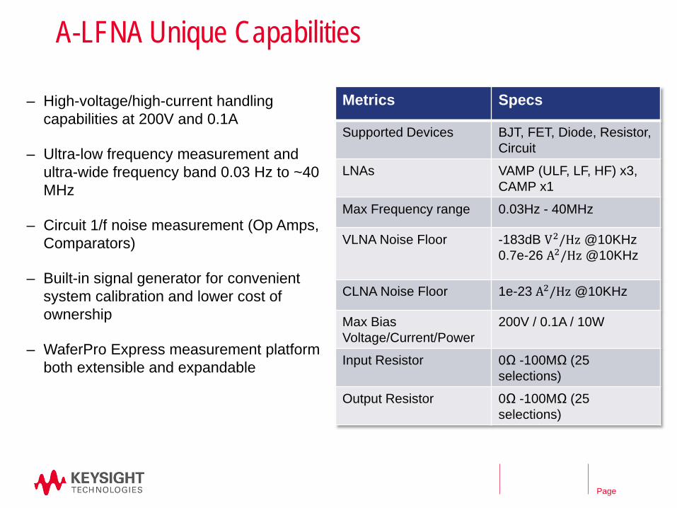
A-LFNA Unique Capabilities
– High-voltage/high-current handling capabilities at 200V and 0.1A
– Ultra-low frequency measurement and ultra-wide frequency band 0.03 Hz to ~40 MHz
– Circuit 1/f noise measurement (Op Amps, Comparators)
– Built-in signal generator for convenient system calibration and lower cost of ownership
– WaferPro Express measurement platform both extensible and expandable
Metrics Specs
Supported Devices BJT, FET, Diode, Resistor, Circuit
LNAs VAMP (ULF, LF, HF) x3, CAMP x1
Max Frequency range 0.03Hz - 40MHz
VLNA Noise Floor -183dB V2/Hz @10KHz0.7e-26 A2/Hz @10KHz
CLNA Noise Floor 1e-23 A2/Hz @10KHz
Max Bias Voltage/Current/Power
200V / 0.1A / 10W
Input Resistor 0Ω -100MΩ (25 selections)
Output Resistor 0Ω -100MΩ (25 selections)
Page
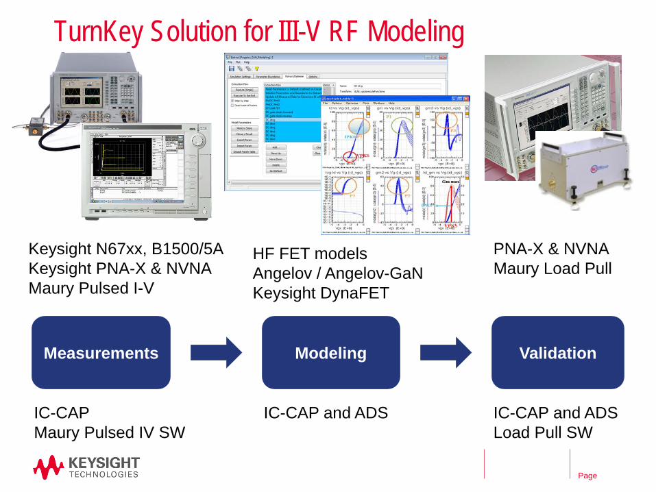
TurnKey Solution for III-V RF Modeling
Measurements Modeling Validation
Keysight N67xx, B1500/5AKeysight PNA-X & NVNAMaury Pulsed I-V
IC-CAPMaury Pulsed IV SW
HF FET modelsAngelov / Angelov-GaNKeysight DynaFET
IC-CAP and ADS IC-CAP and ADSLoad Pull SW
PNA-X & NVNAMaury Load Pull
Page
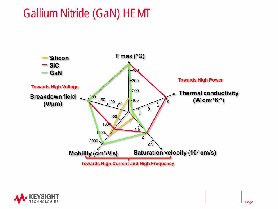
Gallium Nitride (GaN) HEMT
Page
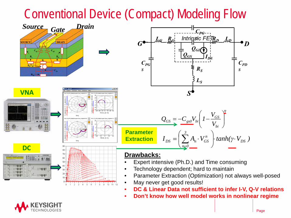
Conventional Device (Compact) Modeling Flow
η
−−=
bi
GSbigs0GS V
V1VCQ
)Vtanh(γVAI DS
3
0n
nGSnDS ⋅⋅
⋅= ∑
=
VNA
DC
Parameter Extraction
Gate DrainSource
Drawbacks:• Expert intensive (Ph.D.) and Time consuming• Technology dependent; hard to maintain• Parameter Extraction (Optimization) not always well-posed• May never get good results!• DC & Linear Data not sufficient to infer I-V, Q-V relations• Don’t know how well model works in nonlinear regime
Page
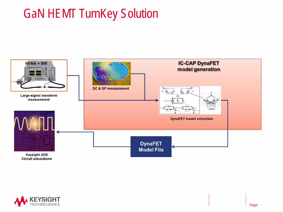
GaN HEMT TurnKey Solution
Page
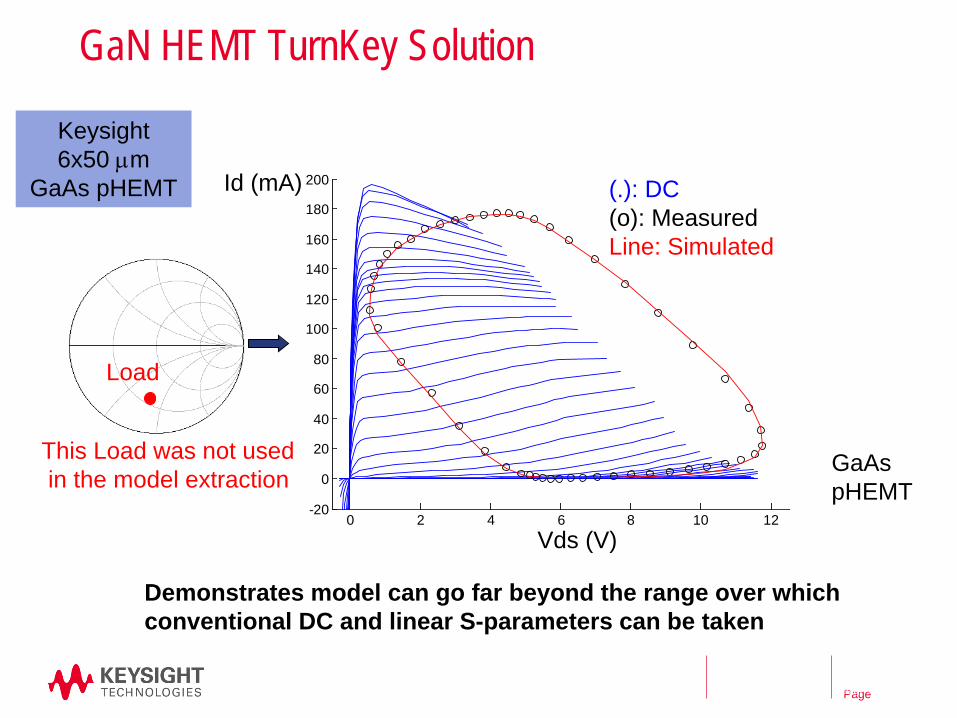
0 2 4 6 8 10 12-20
0
20
40
60
80
100
120
140
160
180
200
Vds (V)
Id (mA) (.): DC(o): MeasuredLine: Simulated
Load
This Load was not usedin the model extraction
Demonstrates model can go far beyond the range over which conventional DC and linear S-parameters can be taken
GaAspHEMT
7/23/2014Amplifier Design Flow Seminar
Keysight6x50 µm
GaAs pHEMT
GaN HEMT TurnKey Solution
Page
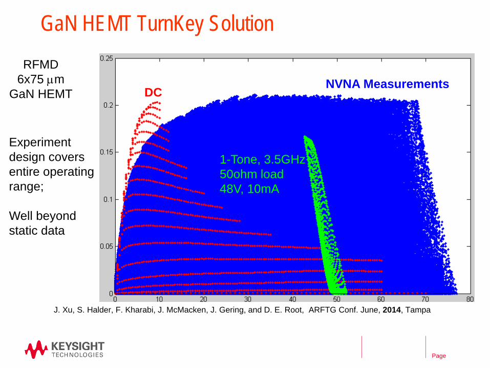
1-Tone, 3.5GHz50ohm load48V, 10mA
J. Xu, S. Halder, F. Kharabi, J. McMacken, J. Gering, and D. E. Root, ARFTG Conf. June, 2014, Tampa
RFMD 6x75 µm
GaN HEMT
Experiment design covers entire operating range;
Well beyond static data
NVNA MeasurementsDC
GaN HEMT TurnKey Solution
Page
10 20 30 40 50 600 70
0.05
0.10
0.15
0.00
0.20
Vdrain
Idra
in_m
eas
I_dr
ain.
i
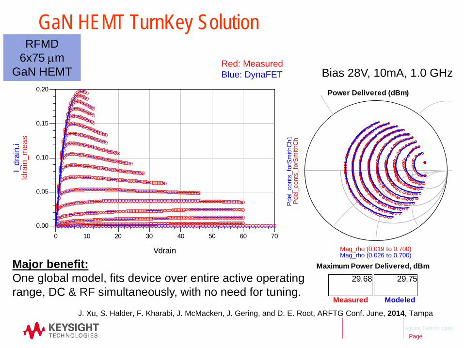
29.68Maximum Power Delivered, dBm
Power Delivered (dBm)
Mag_rho (0.019 to 0.700)
Pde
l_co
nts_
forS
mith
Ch
Mag_rho (0.026 to 0.700)
Pde
l_co
nts_
forS
mith
Ch1
29.75
Measured Modeled
Bias 28V, 10mA, 1.0 GHz
J. Xu, S. Halder, F. Kharabi, J. McMacken, J. Gering, and D. E. Root, ARFTG Conf. June, 2014, Tampa
.
RFMD 6x75 µm
GaN HEMT
Major benefit:One global model, fits device over entire active operating range, DC & RF simultaneously, with no need for tuning.
Agilent Technologies
Red: MeasuredBlue: DynaFET
GaN HEMT TurnKey Solution
Page
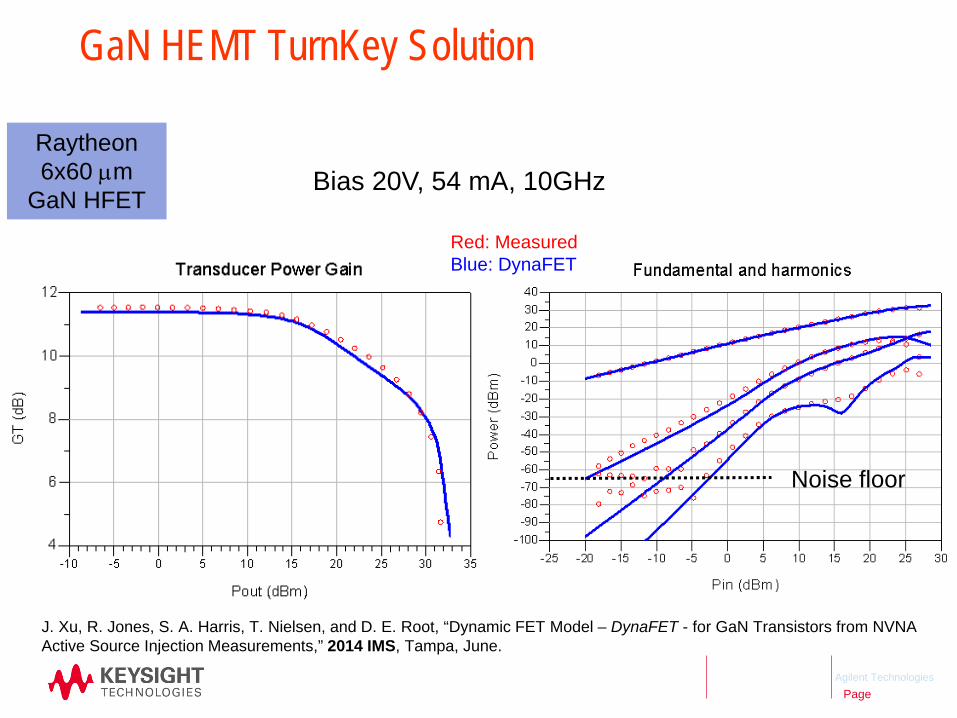
Bias 20V, 54 mA, 10GHz
J. Xu, R. Jones, S. A. Harris, T. Nielsen, and D. E. Root, “Dynamic FET Model – DynaFET - for GaN Transistors from NVNA Active Source Injection Measurements,” 2014 IMS, Tampa, June.
Agilent Technologies
Noise floor
Raytheon 6x60 µm
GaN HFET
Red: MeasuredBlue: DynaFET
GaN HEMT TurnKey Solution
Page
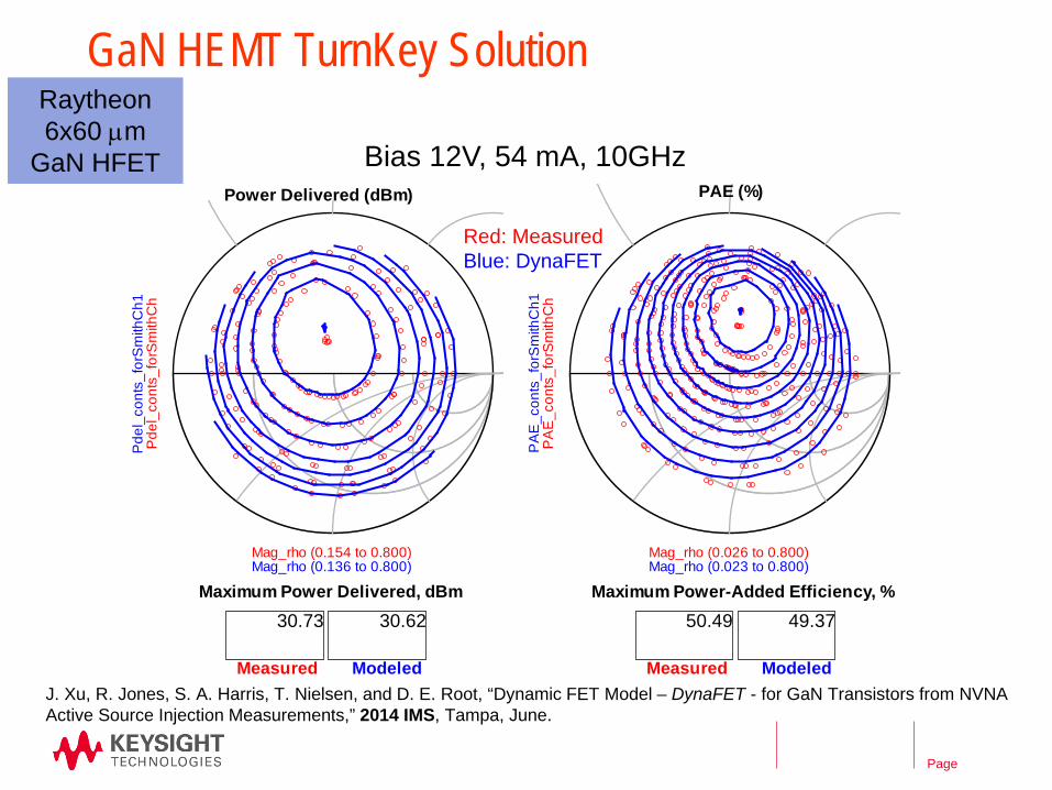
30.73Maximum Power Delivered, dBm
50.49 Maximum Power-Added Efficiency, %
Power Delivered (dBm)
Mag_rho (0.154 to 0.800)
Pde
l_co
nts_
forS
mith
Ch
Mag_rho (0.136 to 0.800)
Pde
l_co
nts_
forS
mith
Ch1
Mag_rho (0.026 to 0.800)P
AE
_con
ts_f
orS
mith
Ch
Mag_rho (0.023 to 0.800)
PA
E_c
onts
_for
Sm
ithC
h1
PAE (%)
30.62 49.37
Measured Modeled Measured Modeled
Bias 12V, 54 mA, 10GHz
J. Xu, R. Jones, S. A. Harris, T. Nielsen, and D. E. Root, “Dynamic FET Model – DynaFET - for GaN Transistors from NVNA Active Source Injection Measurements,” 2014 IMS, Tampa, June.
Raytheon 6x60 µm
GaN HFET
Red: MeasuredBlue: DynaFET
GaN HEMT TurnKey Solution
Page
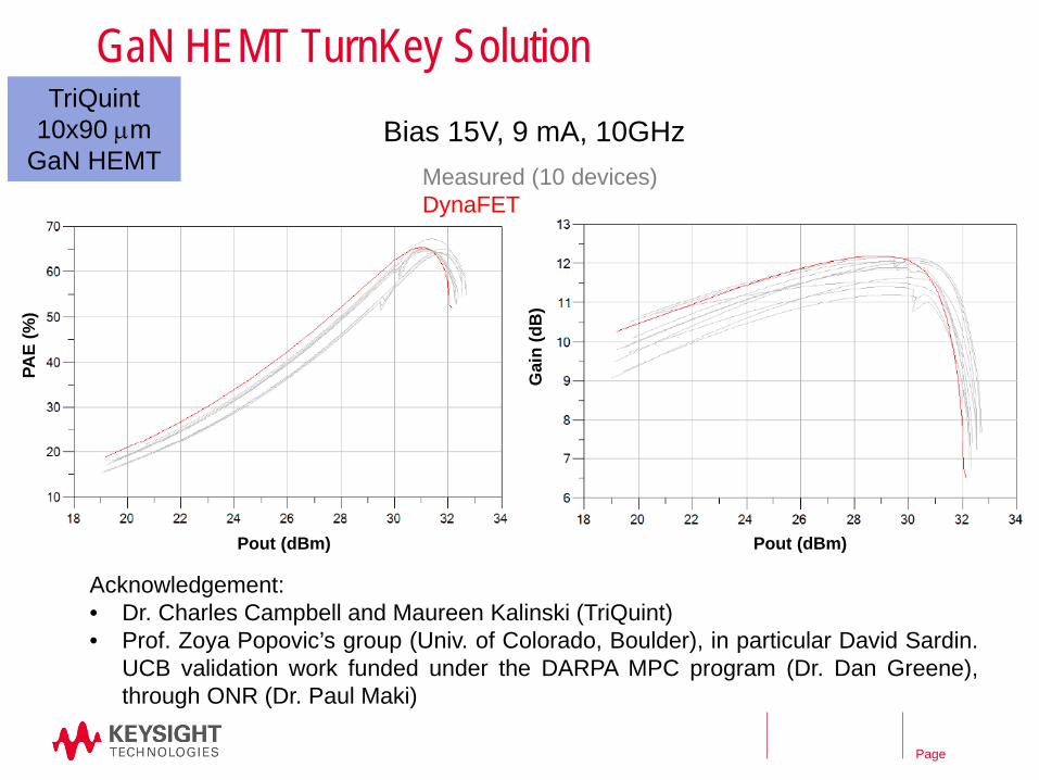
TriQuint10x90 µm
GaN HEMT
Pout (dBm)
PAE
(%)
Pout (dBm)G
ain
(dB
)
Acknowledgement:• Dr. Charles Campbell and Maureen Kalinski (TriQuint)• Prof. Zoya Popovic’s group (Univ. of Colorado, Boulder), in particular David Sardin.
UCB validation work funded under the DARPA MPC program (Dr. Dan Greene),through ONR (Dr. Paul Maki)
Bias 15V, 9 mA, 10GHzMeasured (10 devices)DynaFET
GaN HEMT TurnKey Solution

Page
Silicon Baseband Modeling Turnkey Solution
Page
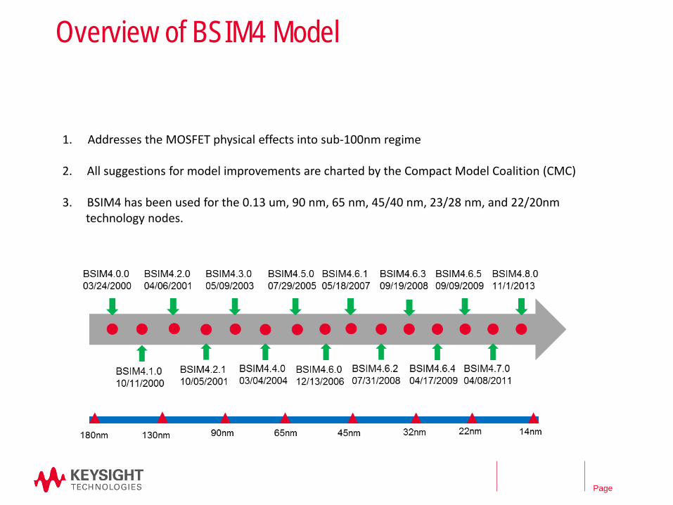
Overview of BSIM4 Model
1. Addresses the MOSFET physical effects into sub-100nm regime
2. All suggestions for model improvements are charted by the Compact Model Coalition (CMC)
3. BSIM4 has been used for the 0.13 um, 90 nm, 65 nm, 45/40 nm, 23/28 nm, and 22/20nm technology nodes.
Page
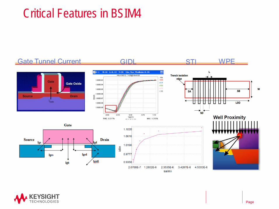
Critical Features in BSIM4
Page
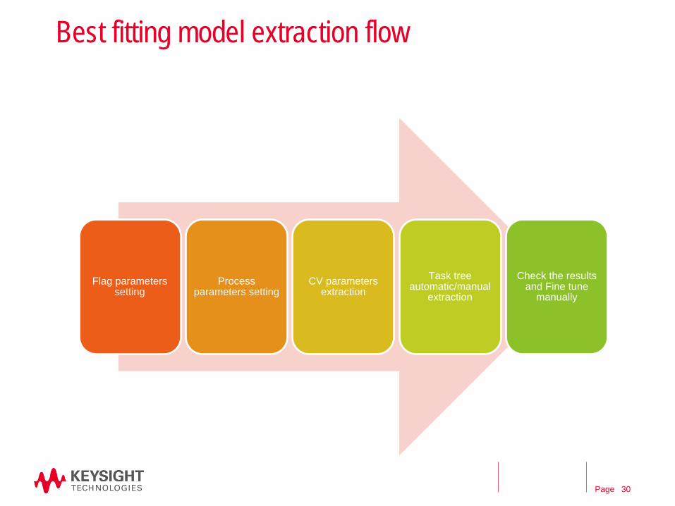
Best fitting model extraction flow
30
Flag parameters setting
Process parameters setting
CV parameters extraction
Task tree automatic/manual
extraction
Check the results and Fine tune
manually
Page
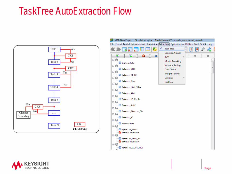
TaskTree AutoExtraction Flow
Page
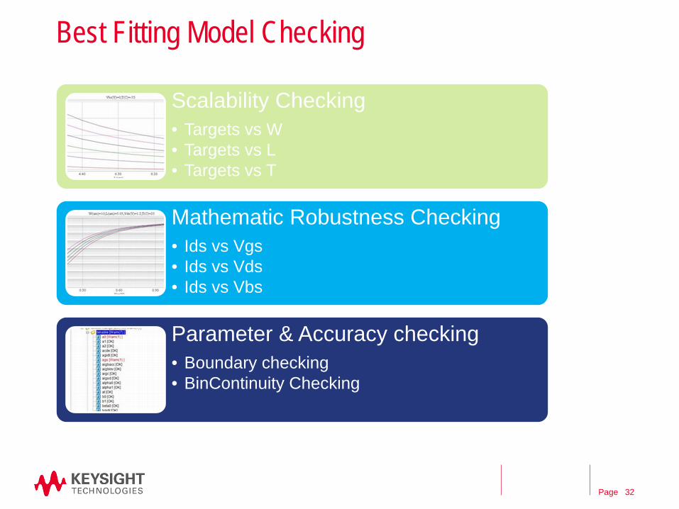
Best Fitting Model Checking
32
Scalability Checking• Targets vs W• Targets vs L• Targets vs T
Mathematic Robustness Checking• Ids vs Vgs• Ids vs Vds• Ids vs Vbs
Parameter & Accuracy checking• Boundary checking• BinContinuity Checking
Page
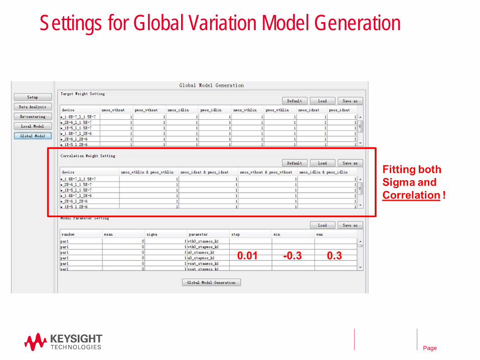
Statistical Simulation and Modeling
– The types of statistical simulation techniques used dictates the types of statistical models that are required
• Corner simulations require corner models
• MC simulations need distributional models
• mismatch analysis needs mismatch models
– Modeling Techniques
• Corner Modeling
• Numerical approaches
• Forward propagation of variance (FPV)
• Backward propagation of variance (BPV)
Page
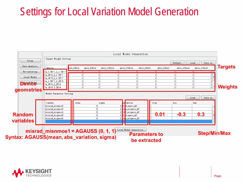
Settings for Local Variation Model Generation
Page
Settings for Global Variation Model Generation
Page
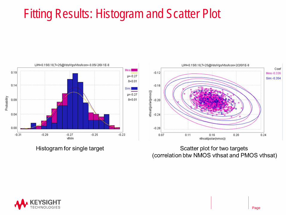
Fitting Results: Histogram and Scatter Plot
Page
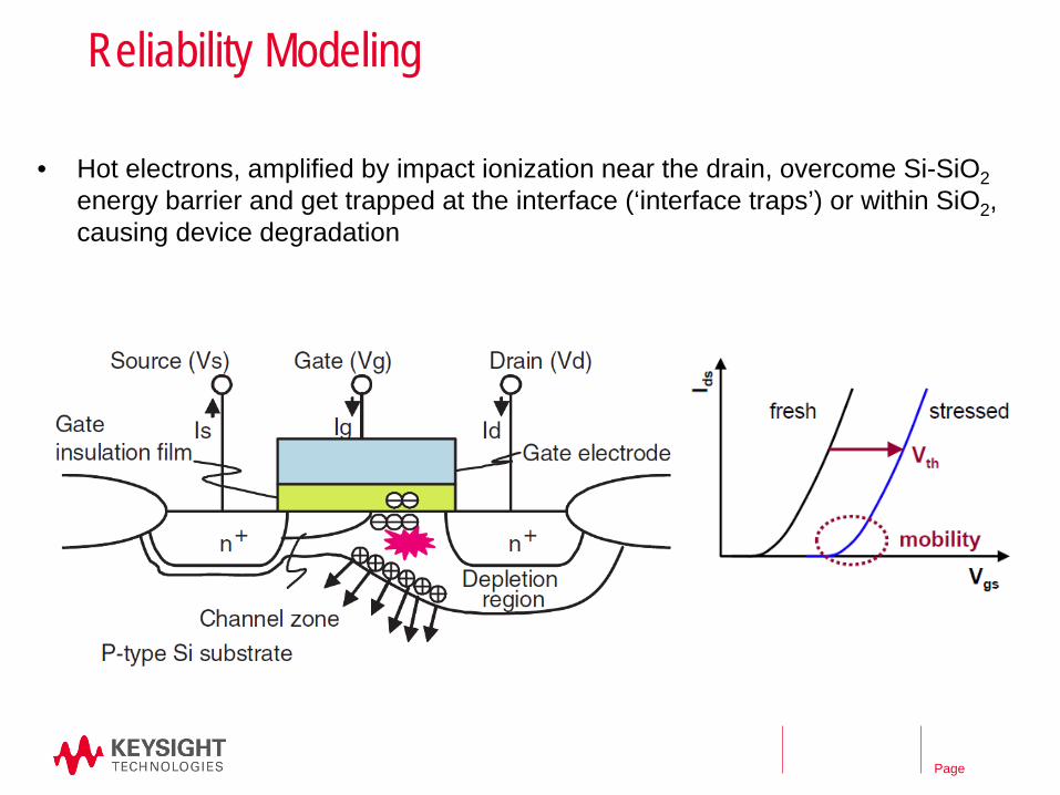
Reliability Modeling
• Hot electrons, amplified by impact ionization near the drain, overcome Si-SiO2energy barrier and get trapped at the interface (‘interface traps’) or within SiO2, causing device degradation

Page
Aging Parameter Extraction
• Vt shift related aging parameters extracted first- Vt dependences on stress time and stress Vgs used
simultaneously
Page
Aging Parameter Extraction
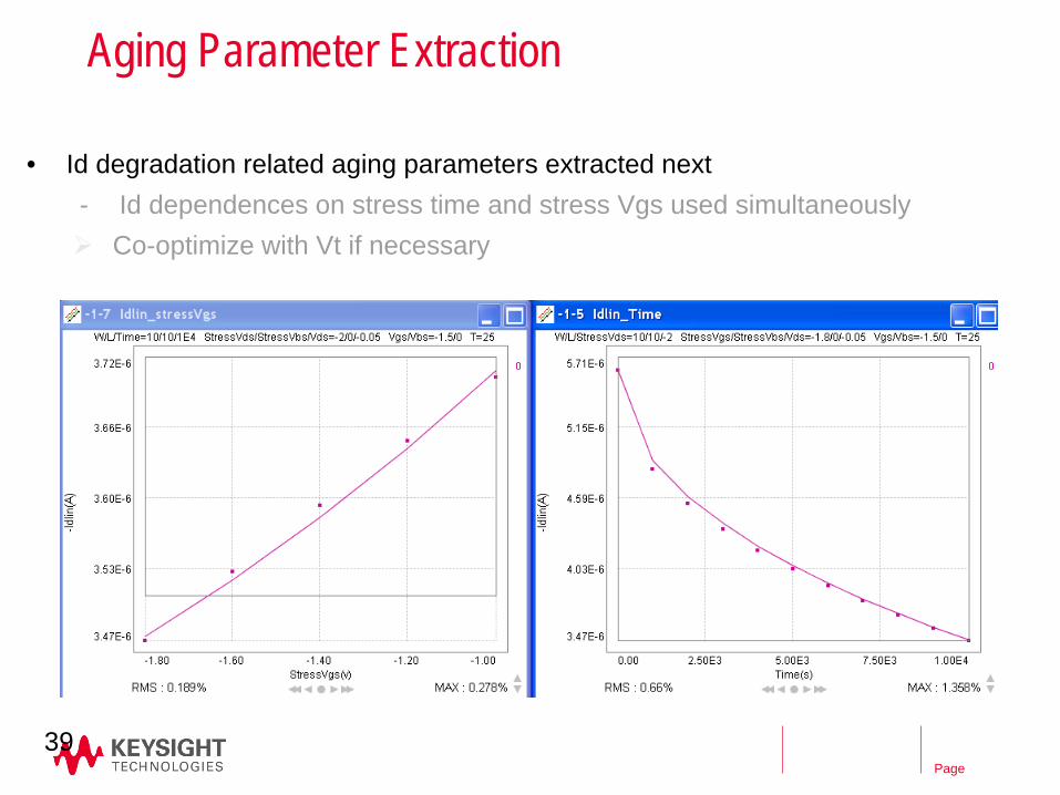
• Id degradation related aging parameters extracted next- Id dependences on stress time and stress Vgs used simultaneously Co-optimize with Vt if necessary
39
Page
Model QA Challenges
– Matrix of support across simulators, technology types, process nodes, fabs, exponentially growing, and so is the complexity
– Requirement to quickly assess how models operate in design space of interest (models are not qualified for all regions)
– Internal scripts no longer sufficient to handle validation requirements
– Need to assess model quality
– Need to compare between models
– Need to automate documentation process
– Model issues detected late in design flow- costly
Page
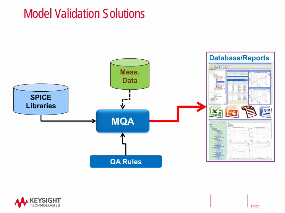
Model Validation Solutions
Page
Model Validation Solutions
– MQA provides significant model verification productivity increase over scripting/manual methods, oftentimes over 10x.
– MQA provides and automated method to validate model performance in your design space of interest thereby assuring comprehensive coverage
– MQA will assess a model’s quality, uncovering hidden issues, and avoiding costly errors later in the design cycle that would quite costly to rectify
– MQA can generate documentation in an automated fashion –productive.
– Enables enhanced communication with design teams
Page
Conclusions
– Keysight provides complete solutions for device modeling from measurement to modeling and model validation.
– WaferProExpress is an easy-to-use automatic on-wafer measurement solution including Low-Frequency Noise measurement.
– ICCAP is a flexible measurement and modeling solution especially for III-V devices and RF devices.
– MBP provides turn-key solutions for silicon technologies including FinFET, PD-SOI and FD-SOI.
– MQA is a model validation solution not only for foundries but also for design houses.