Embed Size (px)
Citation preview
Diffusion of potentialp-type dopants inmonocrystalline ZnO
Eva Holthe EnoksenMaster’s Thesis, Spring 2016
AbstractDiffusion of potential p-type dopants in monocrystalline ZnO
The diffusion of Ag and Cu in monocrystalline ZnO has been investigated by isochronal
annealing and probed with a Secondary ion mass spectrometer. The diffusion was
manipulated by altering the Fermi level position and the stoichiometry of the sam-
ple. For Ag in ZnO, no diffusion was observed at detectable concentrations
(>1× 10¹⁶ Ag/cm3). However, in Ga-doped ZnO, a diffusion of Ag was observed and
the free diffusion model gave a good fit with the experimental data with an ac-
tivation energy of 3.44 eV and a prefactor of 4.03 cm2/s. For Cu, domains of CuO
formed, altering the matrix. In Ga-doped ZnO, the diffusion of Cu was fitted to the
reaction-diffusion model, resulting in an activation energy of 2.72 eV and a prefac-
tor of 15.5 cm2/s. Diffusion of both Ag and Cu was enhanced for high Fermi level
positions, indicating a vacancy-mediated diffusion. However, the resulting activa-
tion energies and prefactors were higher than expected, indicating an interstitial
diffusion component.
SamandragDiffusjon av potensielle p-type dopantar i monokrystallinsk ZnO
Diffusjon av Ag og Cu i monokrystallinsk ZnO er studert ved isokron varmebe-
handling og måling med sekundærionemassespektrometer. Diffusjonen vart ma-
nipulert ved å endre posisjonen til Ferminivået og støkiometrien til prøva. For Ag i
ZnO vart det ikkje observert diffusjon ved målbare konsentrasjonar (>1× 10¹⁶ Ag/cm3).
I Ga-dopa ZnO vart fridiffusjonsmodellen tilpassa til diffusjonsprofilane med ein
aktiveringsenergi på 3.44 eV og ein prefaktor på 4.03 cm2/s. Det vart danna CuO-
domene når Cu diffunderte inn i ZnO, og desse endra matrisa. I Ga-dopa ZnO vart
diffusjonen av Cu tilpassa til reaksjonsdiffusjonsmodellen, noko som resulterte i
ein aktiveringsenergi på 2.72 eV og ein prefaktor på 15.5 cm2/s. Diffusjonen av både
Ag og Cu vart forsterka når posisjonen til Ferminivået var høg, noko som indikerte
vakansmediert diffusjon. Aktiveringsenergiane og prefaktorane vart likevel høgare
enn venta. Det tyder på ein interstitiell diffusjonskomponent.

Acknowledgements
I will start by thanking my two excellent supervisors, Dr. Klaus Magnus Johansen
and assoc. prof. Lasse Vines. Having both of you invest so much time and effort
into my work has not only made me smarter and wiser, but it has enlightened
the process of discovery in science as something one achieves through discussion.
Thank you also for revising my thesis.
I also want to thank prof. Bengt G. Svensson for introducing me to the field of
semiconductor physics, for providing excellent new perspectives when needed, and
for revising the thesis.
I am very grateful for Thomas Neset Sky and his everlasting patience in teaching
me how to use the SIMS, as well as answering the questions which I was too afraid
to ask anyone else. Thanks also to Heine Nygard Riise, for making the thin films
and teaching me how to use the XRD. Also thanks to Dr. Spyros Diplas for perform-
ing an XPS measurement, Dr.Augustinas Galeckas for the PL-measurements and
Jon Borgersen for the SSRM measurements.
Fortunately, there is more to life than physics. I would like to thank Lillefy, Re-
alistlista, SPAU 2013/2014 and everyone at LENS. It would not have been half as
much fun without you. Finally, thank you, Anja, for making every day weirder and
more wonderfull than I ever knew they could be, and for correcting all my grammar
mistakes.
iii


Contents
Abstract ii
Acknowledgements iii
Contents iv
1 Introduction 1
2 Theory and background 52.1 Defects in crystalline solids . . . . . . . . . . . . . . . . . . . . . . . . . 5
2.1.1 Point defects . . . . . . . . . . . . . . . . . . . . . . . . . . . . . . 82.2 Diffusion in crystalline solids . . . . . . . . . . . . . . . . . . . . . . . . 10
2.2.1 Mathematical models of diffusion . . . . . . . . . . . . . . . . . . 102.2.2 Diffusion mechanisms . . . . . . . . . . . . . . . . . . . . . . . . 122.2.3 Diffusion models and the diffusion coefficient . . . . . . . . . . . 15
2.3 Bandgap and doping in semiconductors . . . . . . . . . . . . . . . . . . 152.3.1 Defects and formation energy . . . . . . . . . . . . . . . . . . . . 17
2.4 Crystalline Zinc Oxide . . . . . . . . . . . . . . . . . . . . . . . . . . . . 192.4.1 Crystal growth . . . . . . . . . . . . . . . . . . . . . . . . . . . . . 192.4.2 Doping of ZnO . . . . . . . . . . . . . . . . . . . . . . . . . . . . . 20
2.5 Previous work . . . . . . . . . . . . . . . . . . . . . . . . . . . . . . . . . 20
3 Experimental techniques and procedure 233.1 Secondary ion mass spectrometry . . . . . . . . . . . . . . . . . . . . . . 23
3.1.1 Principles of sputtering . . . . . . . . . . . . . . . . . . . . . . . . 243.1.2 Analysis . . . . . . . . . . . . . . . . . . . . . . . . . . . . . . . . 253.1.3 Instrumentation . . . . . . . . . . . . . . . . . . . . . . . . . . . . 28
3.2 Other experimental techniques used for characterization . . . . . . . . 283.2.1 X-ray diffractometry . . . . . . . . . . . . . . . . . . . . . . . . . 283.2.2 Energy dispersive spectroscopy . . . . . . . . . . . . . . . . . . . 293.2.3 Photoluminescence spectroscopy . . . . . . . . . . . . . . . . . . 303.2.4 Scanning spreading resistance microscopy . . . . . . . . . . . . 32
3.3 Magnetron sputter deposition . . . . . . . . . . . . . . . . . . . . . . . . 323.4 Experimental procedures . . . . . . . . . . . . . . . . . . . . . . . . . . . 33
3.4.1 Samples and methodology . . . . . . . . . . . . . . . . . . . . . . 333.4.2 Introduction of dopant from thin films . . . . . . . . . . . . . . . 36
v
Contents vi
4 Results 374.1 Characterization of the source films used for Ag and Cu diffusion . . . 374.2 Diffusion of Ag . . . . . . . . . . . . . . . . . . . . . . . . . . . . . . . . . 38
4.2.1 Diffusion of Ag in undoped ZnO . . . . . . . . . . . . . . . . . . . 384.2.2 Diffusion of Ag in Ga-doped ZnO . . . . . . . . . . . . . . . . . . 404.2.3 Diffusion of Ag in Ga-doped ZnO in a Zn-rich atmosphere . . . . 42
4.3 Diffusion of Cu . . . . . . . . . . . . . . . . . . . . . . . . . . . . . . . . . 424.3.1 Diffusion of Cu in undoped ZnO . . . . . . . . . . . . . . . . . . . 424.3.2 Diffusion of Cu in Ga-doped ZnO . . . . . . . . . . . . . . . . . . 474.3.3 Diffusion of Cu in ZnO in a zinc-rich environment . . . . . . . . 474.3.4 Complementary measurements . . . . . . . . . . . . . . . . . . . 47
4.4 Uncertainty in the measurements . . . . . . . . . . . . . . . . . . . . . 51
5 Discussion 555.1 Summary and comparison of results . . . . . . . . . . . . . . . . . . . . 555.2 CuO in ZnO . . . . . . . . . . . . . . . . . . . . . . . . . . . . . . . . . . 57
5.2.1 Indications of CuO . . . . . . . . . . . . . . . . . . . . . . . . . . 575.2.2 Hypothesis for the formation of CuO . . . . . . . . . . . . . . . . 585.2.3 Implications for the resulting profiles . . . . . . . . . . . . . . . 59
5.3 A scenario for the diffusion of Ag/Cu in ZnO . . . . . . . . . . . . . . . . 615.4 Computational results for vacancy-mediated diffusion models . . . . . 62
5.4.1 A model for the diffusion of Ag in GZO . . . . . . . . . . . . . . . 625.4.2 Cu in GZO modelled with the Reaction-diffusion model . . . . . 665.4.3 Comparison of the models . . . . . . . . . . . . . . . . . . . . . . 68
5.5 Comparison to other diffusion experiments . . . . . . . . . . . . . . . . 70
6 Summary 736.1 Conclusion . . . . . . . . . . . . . . . . . . . . . . . . . . . . . . . . . . . 736.2 Suggestions for further work . . . . . . . . . . . . . . . . . . . . . . . . . 74
A Derivation of the diffusion equations 77
B Overview of annealing and characterization of the samples 81
C Impurities in Ag:ZnO annealed at 1300 °C 83
D Results from XPS-measurements 85
E Solubility of Cu in ZnO 87
F Derivation of the expression for Cu′Zn 89
Bibliography 93
Chapter 1
Introduction
The Nobel Prize in Physics 2014 was awarded jointly to Isamu Akasaki, Hiroshi
Amano and Shuji Nakamura "for the invention of efficient blue light-emitting diodes
which has enabled bright and energy-saving white light sources" [1]. While possi-
bly seeming less exciting than the discovery of the Higgs boson which was honoured
the year before, the award was a gloom reminder of what is considered one of hu-
mankinds greatest challenges for the future, namely energy.
Today, 1.3 billion people, mostly in the sub-Saharan Africa and the southern Asia,
are living off the electricity grid [2]. Lack of access to electricity has a great impact
on both the quality of life and the prospects for development. Without electric
light, many rely on kerosene lamps or open fire for studying. Neither of these are
considered safe alternatives, as kerosene lamps emit hazardous fumes and open
fires pose a risk in themselves. The lack of electricity also makes women more
likely to be attacked, both by animals and men.
At the same time as the lack of electricity is impeding large parts of the world, the
use of energy by those who have access to it may very well cripple us all. The use
of fossil fuels and subsequent emission of greenhouse gases into the atmosphere
leading to a global warming is now a well-established reality [3].
Although semiconductor technologies may have played a role in augmenting the
need for energy, it is also vital for the solution of these problems. Photovoltaic cells
that convert electromagnetic radiation to electricity is a clean, reliable and scalable
technology. Using the ever-abundant energy from the sun, new technology can be
created which conveniently will work best in the areas where it is needed the most.
Silicon has been the dominant material for solar cells. However, if photovoltaics
is to take a more leading role in the world’s energy production, new candidates for
1
Chapter 1. Introduction 2
materials are needed. One of these is Zinc Oxide (ZnO). ZnO is a wide-bandgap
semiconductor and a transparent conductive oxide (TCO) [4]. ZnO is both cheaper,
more abundant and more environmentally friendly than Indium Tin Oxide (ITO),
which is the most used TCO to date [5, p. 24].
Our understanding of ZnO is still limited. Particularly troublesome is the difficul-
ties in making p-type ZnO, which leaves us unable to utilize the full potential of
ZnO, including fabricating blue and white Light Emitting Diodes (LED’s) from ZnO
alone. But the history may still give us hope. Gallium Nitride (GaN), the material
for which Akasaki, Amano and Nakamura were awarded the Nobel Prize in physics,
is an example of a material in which researchers have overcome the challenge of
creating a p-type substrate. Up until 1990, all GaN was grown n-type, which was
attributed to nitrogen vacancies. However, with the help of both experiments and
Density functional theory (DFT) calculations, it gradually became clear that un-
intentional impurities were to blame [6, 7]. More specifically, hydrogen had been
incorporated in the material, which passivated the defects [8]. Once discovered, it
could also be removed and thus p-type GaN could be fabricated. However, while the
discovery of p-type GaN was extraordinary, a p-type ZnO is highly desired because
it could mean cheaper and more environmentally friendly LED’s.
In order to tackle the challenge of p-type ZnO, we will leave the pratical applica-
tions and delve into the fundamental physics of semiconductors. Solids are often
regarded as static and definite. Although incorrect, this notion is understandable,
as most of us have far more experience with the mixing of liquids or gases than the
mixing of solids. The concept of diffusion in solids challenges this misconception.
Diffusion is "the process whereby particles of liquids, gases, or solids intermingle
as the result of their spontaneous movement caused by thermal agitation and in
dissolved substances move from a region of higher to one of lower concentration"
[9]. As the definition above lets on, diffusion takes place in all phases, but the rate
of the diffusion varies greatly.
Diffusion can be viewed as the macroscopic result of microscopic, atomistic jumps.
These processes give information about which atomic and ionic species exist in our
material and whether a species is mobile or not. This can further yield important
insights into how the materials behave, and how white and blue LEDs from ZnO
could be made. Thus, there is not just a link between the microscopic atomistic
movements and the macroscopic diffusion process, but also, on quite another scale,
between the microscopic diffusion process on one hand, and the macroscopic prob-
lem of solving the energy challenge of our future. If we are to solve these problems,
we must neither forget the microscopic, nor the macroscopic picture.
Chapter 1. Introduction 3
Donors like Al and Ga have been extensively studied, and are mainly found on Zn
sites [10]. It has recently been shown that Al diffuse via a vacancy mechanism by
forming a mobile complex with v′′Zn [11]. The charges of Al and vZn are opposite, and
the two defects are attracted to each other so that the complex is readily formed. In
contrast to the above example with Al, the charge state between the acceptors and
vZn is expected to lead to repulsion and not attraction. Thus the resulting diffusion
process is expected to be quite different. Crucial questions in the pursuit to under-
stand acceptors in ZnO is therefore how a negative effective charge will affect the
migration paths and activation energies, and how the acceptors will interact with
native defects.
This thesis will explore the mechanisms of diffusion for Ag and Cu, two acceptor
dopants [12–18]. Ag is considered a potential p-type dopant, and p-type ZnO doped
with Ag has been reported by several authors [19, 20], but is not widely accepted.
There is substantial interest in Cu due to the potential of Cu2O-ZnO tandem pho-
tovoltaic cells [21, 22], where the properties of Cu in ZnO are relevant to the Cu2O-
ZnO interface, but also because Cu contamination is common in ZnO samples.
The main analysis tool for this exploration is secondary ion mass spectrometry
(SIMS), which can be used to count atoms in a material by measuring the con-
centration vs. depth profile of an element. To introduce the dopant into the ZnO, a
thin-film of ZnO doped with Cu or Ag is deposited on the substrate. The diffusion
is studied by sequentially annealing and probing the material with SIMS, before
annealing again at a higher temperature. Both Cu and Ag were studied under dif-
ferent conditions, effectively manipulating the diffusion process. Additional optical
and electrical measurements were used to gain complementary information, either
about the films or the diffusion process.
This thesis explores these questions by departing from the methodology used by
[11]. For Ag, a behaviour similar to that seen by Azarov et al. was expected. How-
ever, it became clear relatively early that the diffusions were not similar. As the
resulting SIMS profiles did not ressemble any of the known diffusion profiles pre-
sented above, a range of additional techniques were used to investigate the nature
of the aquired SIMS profiles. The resulting thesis is therefore exploratory and to
a large extent qualitative. However, it may hopefully serve as a starting point for
further studies.
The thesis consists of five parts. In Chapter 2, the theory of defects in crystalline
solids, diffusion, semiconductors and ZnO is presented, as well as previous work on
diffusion. Chapter 3 explains the experimental techniques used in this study. The
emphasis will be on SIMS, the main technique used in this work. In Chapter 4,

Chapter 1. Introduction 4
the results obtained will be presented. The results will be discussed and compared
to other relevant works in Chapter 5, and a scenario to explain the results will be
suggested. Finally, Chapter 6 summarizes the thesis and suggests further work.
Chapter 2
Theory and background
This chapter will introduce the theoretical concepts and previous work relevant to
this master thesis. Together with Chapter 3 it forms the theoretical backdrop for
understanding the results presented in Chapter 4. The chapter will first cover the
theory of crystalline solids including defects and diffusion in Sections 2.1 and 2.2,
respectively. Then, a short introduction to bandgap and doping in semiconductors
will be given in Section 2.3 before relevant properties of ZnO will be discussed in
Section 2.4. Finally, previous work on diffusion will be discussed in Section 2.5.
2.1 Defects in crystalline solids
A prerequisite for studying defects in crystalline solids is the notion of a crystal.
A perfect crystal is a three-dimensional periodic array of identical buildning blocks
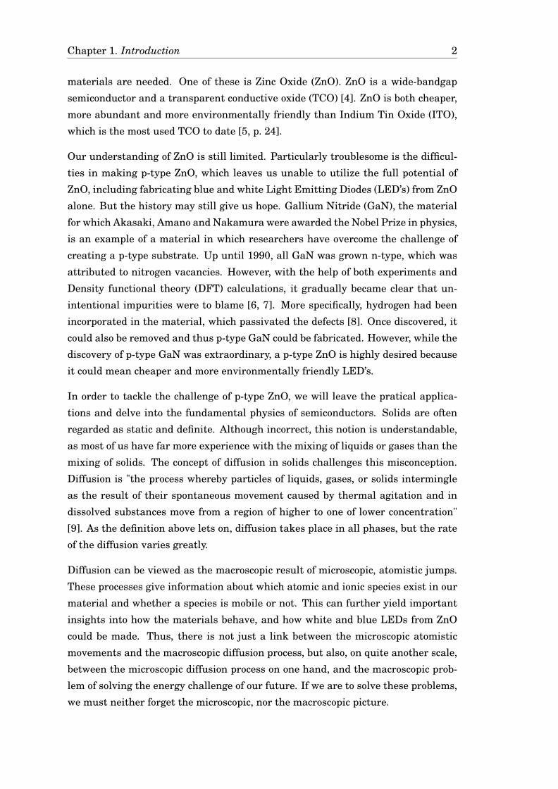
[24]. Formally, a crystal is described by two elements, a lattice and a basis as shown
in Figure 2.1 on page 6. The basis is the buildning block of the crystal. It can be one
or several atoms, or it can be a molecule. These buildning blocks are distributed
in space according to the lattice, which describes a set of mathematical points to
which the basis is attached.
But why are crystalline materials considered in the first place? According to Kittel,
"The important electronic properties of solids are best expressed in crystals" [24,
p. 3]. When theories are formulated in physics, one will often start from a simple
model, before taking into account different complications to this model. For solids,
the perfect crystalline solid is the simplest material in that it can be completely
described by a lattice and a basis. By formulating theories for the simplest material,
other materials can later be viewed as perturbations to the simple theory.
5
Chapter 2. Theory and background 6
Space lattice Basis Crystal structure
FIGURE 2.1: The crystal can be thought of as constructed from a basis and alattice.
Figure 2.1 describes a perfect crystal. However, for all temperatures above 0 K,
a crystal with defects is thermodynamically favoured to a crystal without defects.
This can be shown using either classical or statistical thermodynamics. As an il-
lustration, the equilibrium concentration of single vacancies in a solid will be cal-
culated below. The calculation is adapted from [25] and [26].
To start, the number of possible configurations of Nv vacancy sites in a crystal with
N lattice sites will be considered. Using combinatorics, the number of possible
configurations, Ω, is given as
Ω =N !
Nv!(N −Nv)!. (2.1)
The total entropy for a crystal is given as
∆S = ∆Sm +Nv∆Svib, (2.2)
where ∆Svib is the vibrational entropy for one atom and ∆Sm is the configurational
entropy which stems from the arrangement of atoms. The configurational entropy,
∆Sm1 is:
∆Sm = kB ln Ω (2.3)1The configurational entropy is also called the entropy of mixing, hence the index m.
Chapter 2. Theory and background 7
Here, kB is Boltzmann’s constant.
Because both N and Nv are large, Sterling’s approximation can be used to simplify
the expression:
∆Sm = kB ln Ω (2.4)
= kB ln
(N !
Nv!(N −Nv)!
)(2.5)
= kB (N lnN −Nv lnNv − (N −Nv) ln(N −Nv)) (2.6)
= kBN lnN
N −Nv− kBNv ln
Nv
N −Nv(2.7)
A dilute solution will be considered, that is, Nv << N . Then, N − Nv ≈ N . This
means that the first term in the equation above can be simplified to kBN lnN
N −Nv≈
kBN lnN
N= 0. The second term can also be simplified, so that
∆Sm ≈ −kBNv lnNv
N(2.8)
The change in standard Gibbs’ free energy is given as
∆Gv = Nv∆H − T∆S (2.9)
= Nv(∆H − T∆Svib)− T∆Sm, (2.10)
where T is the temperature in Kelvin. By substituting the expression above for
∆Sm, the following equation is obtained:
∆Gv = Nv(∆H + T∆Svib) + kBTNv ln
(Nv
N
). (2.11)
Here, ∆H is the formation enthalpy for a vacancy, and ∆Svib is the change in vi-
brational entropy. Since the equilibrium concentration of vacancies is of interest,
Gibbs’ free energy will be minimized with respect to the vacancy concentration to
find the equilibrium concentration:
∂∆Gv∂Nv
≈ ∆H − T∆Svib + kBT lnNv
N(2.12)
Since the change in ∆Gv must be zero at equilibrium andNv
Nrepresents the fraction
of vacant sites in a crystal, the fraction of vacant sites in a crystal can be written
Chapter 2. Theory and background 8
as
lnNv
N= ∆H − T∆Svib (2.13)
Nv
N= exp
(∆SvibkB
)exp
(−∆H
kBT
)(2.14)
The first exponential will never be zero and the second one approaches 0 when T
approaches 0 K. Thus, at any temperature T > 0 K, the solid will contain vacancies.
The higher the temperature or the lower the formation enthalpy, ∆H, the greater
the ratio Nv/N will be. Similar arguments can be made for other point defects. The
reader is referred to [25] for these.
So far, it has been established that all crystals above 0 K contain defects. This
statement has been exemplified with a derivation of the number of vacancies in a
crystal. However, the notion of a defect has not been explicitly defined.
All deviations from a perfect crystal are referred to as defects. This is true re-
gardless of whether the defect is intentional or not. The defects can be charac-
terized according to their dimensionality. The simplest form of defects are called
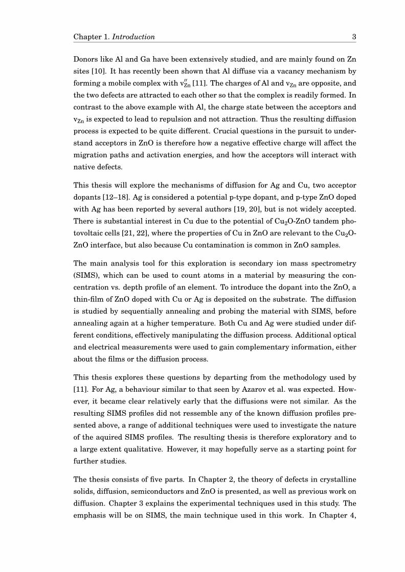
zero-dimensional defects, or point defects. This includes defects such as vacancies,
interstitials, dopant atoms etc. Point defects will play an important role in this
thesis, and will therefore be treated more thoroughly in Section 2.1.1.
One-dimensional defects, on the other hand, extend in one direction throughout
the crystal. These are also called line defects. The most common line defect is a
dislocation, i.e., an extra line of atoms inserted between two other lines of atoms.
Two-dimensional defects are also called planar defects. These include polycrys-
talline grain boundaries, surfaces and stacking faults. Three-dimensional defects,
or bulk defects, are irregularities in all dimensions. A common bulk defects is a
precipitate, i.e., a second phase suspended in the crystal.
2.1.1 Point defects
This section relies heavily on Campbell’s treatment of defects in [27]. As men-
tioned, point defects deserve special attention because of their vital importance in
understanding diffusion mechanisms and doping. The most common point defects
are shown in Figure 2.2 on page 9.
Point defects can be divided into two main groups, namely intrinsic and extrinsic
defects. Vacancies and self-interstitials are intrinsic defects, because they can be
Chapter 2. Theory and background 9
VacancyInterstitial
impurity
Substitutional
impuritySelf-interstitial
Intrinsic
defectsExtrinsic
defects
FIGURE 2.2: Important point defects in crystals include vacancies, interstitialsand impurities.
viewed simply as displaced atoms from the host structure. As argued above, these
defects will be present in any solid above 0 K. A vacancy is an atom missing from
the lattice. A self-interstitial, on the other hand, is a lattice atom displaced to an
interstitial site. Sometimes, a vacancy and a self-interstitial are created simulta-
neously (not shown in Figure 2.2). In that case, the resulting defect is called a
Frenkel defect. Extrinsic defects are caused by impurity atoms residing on either
a lattice site or an interstitial site. In the former case, the defect is also referred to
as a substitutional impurity. Dopant atoms, which are treated in Section 2.3, are
usually substitutional impurities.
The above description of defects is simplified, as it assumes that the solid is ele-
mental. In compounds such as ZnO, there is additional possible defects such as
antisite defects, where a zinc atom resides on an oxygen site and vice versa. These
are treated in more detail in ref. [28, pp. 11-14].
Point defects are most easily described using Kröger-Vink notation. The notation
let us describe both the species X, the relative charge q and the site s using Xqs. The
charge is given as relative to the matrix. Thus, a zinc atom on a zinc site can be
described as Zn×Zn, where x is the symbol for neutral charge. Positive and negative
charges are denoted with superscript dot, , and superscript prime, ′, respectively,
so that an oxygen vacancy will be denoted vO and an oxygen interstitial will be
denoted O′′i . The lower-case v for a vacancy and i for an interstitial are adopted as
suggested in [26] to avoid any possible confusion with the elements iodine (I) and
vanadium (V).
Chapter 2. Theory and background 10
2.2 Diffusion in crystalline solids
Diffusion has been a topic of great interest throughout both the 19th and the 20th
century. However, the approaches to diffusion have varied, which leads us to two
very different ways of studying and describing diffusion. Both these approaches
have their merits; Section 2.2.1 will treat diffusion as a deterministic process in a
continuous media, while Section 2.2.2 will treat diffusion as a stochastic process
happening at the atomic level. This division is inspired by Glicksman [29].
2.2.1 Mathematical models of diffusion
As Fick demonstrated already in 1855, diffusion can be viewed as a macroscopic
process in a continuous media and using differential equations [30]. Fick was in-
spired by Fourier’s heat equation, which had been published nearly half a century
before his results on diffusion as well as Ohm’s law. His goal was "the development
of a fundamental law, for the operation of diffusion in a single element of space"
[30]. This led him to propose the following law, called Fick’s first law:
J(z, t) = −DdCdz
(2.15)
, where J is the flux density,D is the diffusion coefficient and C is the concentration.
Although Fick only postulated the law before he went on to show it experimentally,
a theoretical derivation is also possible, as is shown in Appendix A.
Fick’s first law is called a phenomenological law, because in this form, it simply
describes a physical observation. All the physical processes that take place are
described by the diffusion coefficient D, which contains the jumping frequency and
the distance between the atoms. The minus sign in the equation means that the flux
will always go from regions of high concentration to regions of low concentration,
thus leading to a homogenization. Fick’s first law is derived under the assumptions
that the medium is an isotropic and homogeneous solid [31, p. 3] with a continuous
flux.
Once Fick’s first law is established, it can be combined with the continuity equation
to derive Fick’s second law (also shown in Appendix A):
∂C
∂t= D
∂2C(z, t)
∂z2(2.16)
Chapter 2. Theory and background 11
For most situations, equations 2.15 and 2.16 cannot be solved analytically. How-
ever, there are a few useful exceptions [27].
The first exception is the semi-infinite source model, also called predeposition dif-
fusion. This occurs when the source is fixed at the surface for t > 0. The boundary
conditions are as follows:
C(z, 0) = 0
C(0, t) = Cs
C(∞, t) = 0
Here, Cs is the solubility of the diffusing specie. The solution for these conditions
is:
C(z, t) = Cserfc
(z
2√Dt
), t > 0 (2.17)
Another exception is the drive-in diffusion, where the impurity dose in the sample
remains constant through the diffusion. In this case, the boundary conditions are
C(z, 0) = 0, z 6= 0
dC(0, t)
dz= 0
C(∞, t) = 0∫ ∞0
C(z, t)dz = QT = constant
Where QT is the dose. This gives a gaussian solution:
C(z, t) =QT√πDt
exp
(−z2
4Dt
), t > 0 (2.18)
The two solutions above are mathematically easy, but they will only describe the
resulting behaviour of the diffusing specie, and not what is causing the diffusion.
If one is interested in the diffusion mechanisms, the diffusion must be treated as
stochastic processes at an atomic scale. This will be done in Section 2.2.2. However,
as a bridge between these two ways of looking at diffusion, Fair’s vacancy model will
be considered.
Fair and Tsai formulated their model for the vacancy-mediated diffusion of phos-
phorus in silicon in 1977 by using one diffusion coefficient for every charge state of
the vacancy. Every charge state is then multiplied with the probability of trapping
Chapter 2. Theory and background 12
a charge carrier. This probability is proportional to(n
ni
)qfor a negatively charged
defect, where n is the concentration of electrons, ni is the intrinsic electron concen-
tration and q is the charge state of the vacancy [32]. For a positively charged defect,
the probability is proportional to(p
ni
)q, where p is the concentration of holes. This
gives the following expression for the effective diffusion coefficient:
Deff = D= +D−n
ni+D2−
(n
ni
)2
+ ...+D+ p
ni+D2+
(p
ni
)2
+ ...[27] (2.19)
In theory, third- and fourth order terms could also have been included, but in prac-
tice, they are rarely needed.
In Fair’s vacancy model, the diffusing species moves according to the generalized
Fick’s law as stated in equation A.15 on page 80. However, as the diffusivity indi-
rectly depends on the position, Fick’s law cannot be simplified as is done in equa-
tion 2.16. The incorporation of different charge states gives the ability to account
for more than one diffusion process. Since more diffusion coefficients can be added,
Fair’s vacancy model can always be made to fit a diffusion curve. Although the
model may not give direct insight into the diffusion processes at an atomistic level,
it can nevertheless yield important clues about the charge states involved in the
diffusion.
2.2.2 Diffusion mechanisms
Transitioning from the macroscopic to the microscopic level, diffusion can be treated
as a stochastic process at the atomic scale. With this approach, diffusion is a col-
lection of mechanisms that make an atom jump from one site to another. Six of
these mechanisms will be illustrated here. The first two, the direct exchange mech-
anism and the interstitial mechanism, are examples of direct mechanisms, and are
illustrated in Figure 2.3 on page 13. The former of these demands that at least six
interatomic bonds must be broken, and is therefore more energy-demanding and
less likely to happen compared to e.g. the vacancy mechanism presented below [27,
p. 46]. The interstitial mechanism, however, is the preferred diffusion mechanism
for small impurity atoms. The mechanism is fast compared to other diffusion mech-
anisms, because the bonding between the interstitial impurity and the surrounding
atoms is generally weak.
The last four mechanisms are all indirect mechanisms of diffusion, and are illus-
trated in Figure 2.4 on page 14. They can be divided into two main groups, dopant
Chapter 2. Theory and background 13
(A) Direct exchange (B) Interstitial mechanism
FIGURE 2.3: Direct diffusion mechanisms.
diffusion and hybrid diffusion. Both the vacancy mechanism in Figure 2.4a and the
interstitialcy mechanism in Figure 2.4b are examples of dopant diffusion. Vacancy
mediated diffusion is one of the most important mechanisms of diffusion. Here, an
impurity moves to a vacant lattice site. For this to happen, the vacancy must first
move to a neighbouring site of the impurity. The impurity can then jump into the
empty lattice site. The lattice site formely occupied by the impurity is now a new
vacancy. Compared to the direct exchange mechanism mentioned above, only half
as many bonds have to be broken, and the process is energetically more favourable.
Mathematically, the process can be expressed as
As + V AV, (2.20)
where As is an impurity on a lattice site, V is a vacancy and AV is an impu-
rity–vacancy pair. After the vacancy and the impurity have switched positions, the
complex dissolves for the vacancy to diffuse to a new site so that the process can be
repeated. If the impurity and the vacancy have opposite charges, they will attract
each other. For a neutral impurity and a charged vacancy, the pairing energy will
be similar to that of two neutral species forming a complex [28, p. 123]. For two
negatively or two positively charged species, the Coulomb potential will have to be
overcome for the reaction to happen.
For the interstitialcy mechanism, a self-interstitial displaces the impurity, driving
it into an interstitial site. The mechanism is also called the indirect interstitial
mechanism. The process can be described as
As + I AI, (2.21)
where I is a self-interstitial and AI is an impurity–self-interstitial pair. The in-
terstitialcy diffusion can only happen as long as the pair does not dissociate. The
Chapter 2. Theory and background 14
(A) Vacancy mechanism (B) Interstitialcy mechanism
(C) Frank-Turnbull mechanism (D) Kick-out mechanism
FIGURE 2.4: Indirect diffusion mechanisms.
mechanism is often favoured above interstitial diffusion if the impurity is nearly
equal in size to the lattice atom [33, pp. 100-102]
The last two mechanisms are both examples of hybrid mechanisms, which implies
that the elements involved are dissolved substitutionally, but diffuse interstitially
[34]. The Frank–Turnbull mechanism is also called the dissociative mechanism
(see Figure 2.4c). In this mechanism an impurity is released from a lattice site,
diffusing interstitially until it is trapped by a vacancy, and the process can be de-
scribed as:
As Ai + V, (2.22)
where Ai is a dopant dissolved interstitially.
The kick-out mechanism is illustrated in Figure 2.4d, and involves an impurity that
diffuses interstitially and kicks out a lattice atom on a lattice site to take its place.
The impurity can migrate fast until it dislodges a lattice atom. It can be described
mathematically as
Ai As + I, (2.23)
Both the Frank–Turnbull mechanism and the kick-out mechanism differ from the
interstitialcy method because they do not need a self-interstitial to drive the pro-
cess. The result of the Frank–Turnbull mechanism and the kick-out mechanism
are similar: Both start out with an impurity diffusing interstitially and end with
a less mobile impurity trapped on a lattice site, but unlike the Frank–Turnbull
mechanism, the kick-out mechanism has created a self-interstitial.
Chapter 2. Theory and background 15
2.2.3 Diffusion models and the diffusion coefficient
Diffusion models are developed to link experimental data to diffusion mechanisms.
This is done by assuming a behaviour of the diffusers, which is then modelled and
fitted to the experimental data. Examples of diffusion models are kick-out diffusion
[35], trap-limited diffusion [36] and reaction-diffusion [11], as well as the two ana-
lytical solutions of Fick’s law and Fair’s vacancy model mentioned in Section 2.2.1.
All of these models use the diffusivity as a fitting parameter. The diffusivities at
different temperatures are then plotted in an Arrhenius plot with diffusivity vs. 1/T
to yield the activation energy and the prefactor according to the Arrhenius equa-
tion 2.24.
D = D0 exp(−EakT
). (2.24)
Here, Ea is the activation energy of the diffusion process and D0 is a prefactor with
units cm2/s. This prefactor contains information about the geometry, the jump
frequency and the entropy of the system, and can be written as
D0 = αs2Zν exp(∆Sf + ∆Sm
k), (2.25)
where α is a geometrical factor depending on the structure, s is the distance to
the next-nearest neighbour, Z is the number of adjacent sites to which the atom
can jump, ν is the vibrational frequency and ∆Sf + ∆Sm are the entropy changes
associated with the formation and migration of a defect mediating the diffusion
process, respectively [26].
2.3 Bandgap and doping in semiconductors
When isolated atoms are brought together, the atoms interact and form bonds. The
discrete energy levels of electrons in individual atoms combine to form continuous
energy bands. The highest filled energy band is called the valence band while the
lowest unfilled band is called the conduction band. Electrons can be excited from
the valence band to the conduction band either thermally (for T>0 K) or optically.
The excited electrons leave unfilled states in the valence band. An unfilled state is
named a hole, and is an example of a pseudo-particle [24]. The process in which an
electron and a hole are created simultaneously is called intrinsic ionization.
Chapter 2. Theory and background 16
Electrons in a solid obey Fermi–Dirac statistics with the distribution function
f(E) =1
1 + e(E−EF )/kBT, (2.26)
where f(E) is the probability that an energy state E is occupied. The Fermi level
EF is the energy state in the bandgap with probability 1/2 of being occupied, and is
an important quantity for characterizing semiconductors. According to the Aufbauprinciple, all states below EF should be occupied and all states above EF should be
unoccupied when an atom is in its ground state [37].
Semiconductors can be doped by intentionally introducing impurities into the ma-
terial. If the impurities have a greater number of electrons in the valence shell
than the host, these electrons may form a donor level2. From this level, the impu-
rity atom can donate extra electrons to the conduction band, and the impurity is
labelled a donor. The result is an excess of electrons compared to holes, and the
material is called n-type. Likewise, if the impurity has a lower number of electrons
in the valence shell than the host, an acceptor level may be formed, which can eas-
ily accept electrons, creating holes in the valence band. As a result, there will be an
excess of holes in the valence band compared to electrons in the conduction band,
and the material will be p-type. The energy difference between the donor/acceptor
level and the conduction/valence band determines how easy it is to create excess
charge carriers. One can distinguish between shallow donors, for which the donor
level is near the conduction band and thus easily ionized, and deep donors which
require more energy to ionize. Likewise, there are shallow and deep acceptors.
All solids have their own characteristic energy band structures. Since the energy
bands form when the atoms are brought together, the separation between the con-
duction band and the valence band, the bandgap, Eg, is determined by the structure
of the solid and it is independent of doping for low doping concentration [38]. The
Fermi level position EF will change with doping:
EF = Ei + kBT ln
(n
ni
), (2.27)
EF = Ei − kBT ln
(p
ni
), (2.28)
2Although the level is usually below the conduction band, heavy doping or very shallow defectscan cause it to reside in the conduction band
Chapter 2. Theory and background 17
where Ei is the intrinsic Fermi level position and n/p is the majority charge carrier
concentration [38, p. 93]. The Fermi level position will in turn determine the for-
mation energy for charged defects in the material. Thus, via the charge carrier con-
centration, the dominating defect may, at thermodynamic equilibrium, indirectly
determine the type and amount of other defects in a material.
There can be both donors and acceptors in a material. These can either be the
result of codoping (i.e., doping with both acceptors and donors), native defects or
unintentional impurities in the solid. This leads to compensation of the material
i.e., some of the charge carriers recombine with minority carriers from defects in the
material, and the effective charge carrier concentration is lower than the doping.
In cases of heavy doping, the doping itself can induce the compensation because the
Fermi level position will change, lowering the formation energy of native compen-
sating defects.
2.3.1 Defects and formation energy
There are several possible approaches for considering the effect of defects on a ma-
terial, as explained by Freysoldt et al. [39]. One approach, as is used by Freysoldt
et al. defines and calculates formation energies for all individual defects. This cor-
responds to a grand canonical approach where defect interactions take place via
interactions with an electron reservoir. This is distinct from the approach chosen
by F. A. Kröger [28], who constructs all possible reactions needed to keep the sys-
tem charge neutral. Although formation energy calculations are time-consuming to
carry out, this process avoids the need for assumptions about the reactions occuring
in the material studied.
Density functional theory (DFT) is often used to calculate the formation energies
of defects. DFT is a quantum mechanical computational method used to study the
electronic structure of many-body systems. Contrary to Hartree–Fock methods,
which are based on the calculation of complex many-electron wavefunctions, DFT
uses the spacially dependent electron density as a variable. This reduces the num-
ber of variables for N electrons from 3N to 3, and can greatly reduce computational
costs.
However, DFT calculations are known to be inaccurate when used for calculating
the properties of semiconductors, particularly the band-gap. Hybrid DFT, in which
DFT and the Hartree–Fock method are mixed according to a set fraction, is there-
fore often used to improve the accuracy of the results.
Chapter 2. Theory and background 18
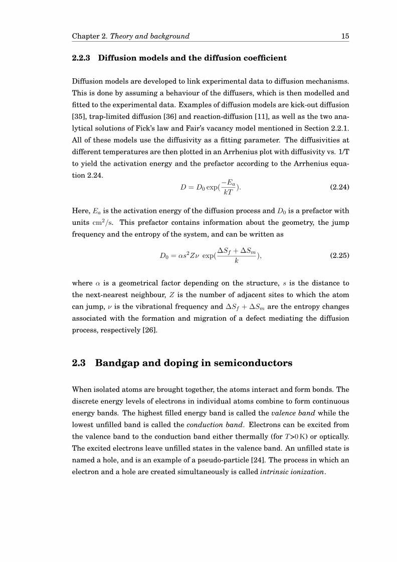
CB
Eform
EFFIGURE 2.5: Illustration of formation energy Eform vs. fermi level EF . Shownin the illustration is three potential charge states of an amphoteric defect and the
charge state transition levels ε between the different charge states.
From DFT calculations, the formation energy, Eform of a certain charge state , q, of
a defect, X, is found from:
Eform[Xq] = ED −∑i
miµi + qEf , (2.29)
where ED is the calculated energy for the defect relative to a perfect crystal, in-
cluding any corrections, mi indicates the number of atoms of type i that have been
added to (mi > 0) or removed from (mi < 0) the system to create the defect and
µi is the corresponding chemical potential. The Fermi level Ef corresponds to the
chemical potential of the electrons [40].
From Section 2.3 it is known that the Fermi level position changes with the charge
carrier concentration. Looking at equation 2.29, it becomes clear that the formation
energy of a donor defect with charge q = +1 will increase when the Fermi level
position increases. Thus, donor defects are more difficult to form when the Fermi
level position is high and when there is an excess of donors. On the other hand,
the formation energy of an acceptor defect with charge q = −1 will decrease when
the Fermi level position decreases. This can result in an intrisic compensating
behaviour of the material as explained above. Formation energies as a function of
the Fermi level position is illustrated in Figure 2.5.
Chapter 2. Theory and background 19
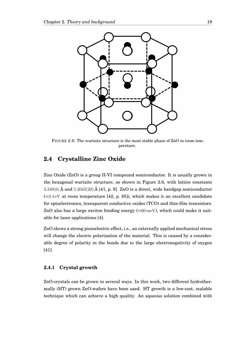
FIGURE 2.6: The wurtzite structure is the most stable phase of ZnO in room tem-perature.
2.4 Crystalline Zinc Oxide
Zinc Oxide (ZnO) is a group II-VI compound semiconductor. It is usually grown in
the hexagonal wurtzite structure, as shown in Figure 2.6, with lattice constants
3.249(6) Å and 5.2042(20) Å [41, p. 9]. ZnO is a direct, wide bandgap semiconductor
(≈3.4 eV at room temperature [42, p. 85]), which makes it an excellent candidate
for optoelectronics, transparent conductive oxides (TCO) and thin-film transistors.
ZnO also has a large exciton binding energy (≈60 meV), which could make it suit-
able for laser applications [4].
ZnO shows a strong piezoelectric effect, i.e., an externally applied mechanical stress
will change the electric polarization of the material. This is caused by a consider-
able degree of polarity in the bonds due to the large electronegativity of oxygen
[41].
2.4.1 Crystal growth
ZnO-crystals can be grown in several ways. In this work, two different hydrother-
mally (HT) grown ZnO-wafers have been used. HT growth is a low-cost, scalable
technique which can achieve a high quality. An aqueous solution combined with
Chapter 2. Theory and background 20
mineralizers are added to an autoclave at elevated temperatures and high pres-
sures. ZnO is dissolved in the solution and then recrystallized, using a seed crystal
to achieve better crystallinity. The mineralizers are usually LiOH and KOH, which
are employed to increase the solubility of ZnO in the solution. LiOH in particular
leads to a high concentration of Li in the final substrate [43].
2.4.2 Doping of ZnO
ZnO suffers from a doping asymmetry issue not unusual in wide-bandgap com-
pound semiconductors. N-type ZnO is easily established, and un-doped ZnO is typi-
cally n-type with a carrier concentration from 1× 10¹⁴ atoms/cm3 to 1× 10¹⁷ atoms/cm3
[44, 45]. This is thought to be caused by both impurities and intrinsic defects.
Higher n-type doping can be achieved by doping. Common n-type dopants include
H, Al, Ga and In [46].
P-type ZnO, on the other hand, is largely an unresolved challenge, although many
reports of p-type ZnO exist (e.g. [19, 20, 47]). Unfortunately, the defects causing
ZnO to be unintentionally n-type increase the difficulty of making p-type ZnO. In
addition, the position of the valence band maximum in ZnO is very low compared to
the vacuum level, and shallow acceptor levels necessary for p-type doping are diffi-
cult to achieve [43, p. 40]. For a more in-depth treatment of the doping asymmetry
issue, see ref. [44].
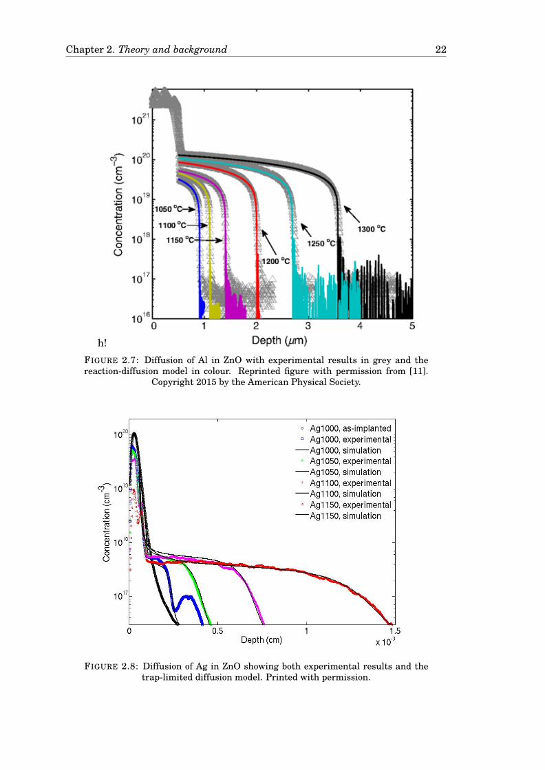
2.5 Previous work
Diffusion in ZnO has been extensively studied through experimental work and a
large number of computational studies. Studies relevant to this work include diffu-
sion studies of H, Li, Ni and Al in ZnO, as well as computational and experimental
studies on Cu and Ag in ZnO. For H, the study by Johansen et al. showed that a
trap- and solubility limited model prevailed [36]. For Li, Knutsen et al. showed
that Li is amphoteric and can act as both a donor on an interstitial site (Lii) and
as an acceptor on a Zn-site (LiZn) [35]. The conversion between mobile Lii and sta-
ble LiZn results in a very sharp gradient. Sky studied the diffusion of Ni in ZnO
and found that Ni diffuses by a combination of vacancy-mediated and interstitial
processes [48]. Finally, Johansen et al. studied the diffusion of Al in ZnO both
experimentally and computationally, and showed that the diffusion is Zn-vacancy
mediated and that the underlying process is a reactive diffusion where Al diffuses
as an AlZnvZn-complex, which may dissociate. The activation energy for the process
Chapter 2. Theory and background 21
is 2.6 eV. These results are presented in [11] and are reprinted with permission for
reference in Figure 2.7 on page 22.
Acceptor dopants, such as Ag and Cu, on the other hand, have been studied far less
extensively than donor dopants. Herklotz, Lavrov, and Weber studied diffusion of
Cu in ZnO. However, as concentrations were determined using Fourier transformed
infrared spectroscopy, the mechanism behind the diffusion is difficult to determine
[49]. Impurities of Cu have also been studied by Gallino and Di Valentin using DFT.
The study predicted that Cui is a single, shallow donor with a (+1/0) thermodynamic
transition level 0.13 eV below the conduction band minimum. It is also reported that
CuZn is an acceptor state with an (0/-1) acceptor transition level between 0.17 eV and
0.19 eV above the valence band, i.e., a rather deep acceptor. It was also reported that
high concentrations of Cu favour clustering [18].
The interest in Ag as a potential p-type dopant is evident in the literature, and
p-type ZnO with Ag dopant has been reported by several sources [19, 20], but is not
widely accepted. Huang, Wang, and Wang carried out first principles calculations
on Li, Na, K and Ag, reporting that Agi is a fast diffuser, with at least a 1.56 eV
barrier to transform to a substitutional site (AgZn). On the other hand, the barrier
to transform from a substitutional to an interstitial site is at least 3.4 eV, meaning
that the stability of AgZn is high [50].
Azarov et al. studied diffusion of interstitial Ag in ZnO. It was shown that at low
temperatures, Zni assists the diffusion of Ag and lead to an Ag pile-up behind the
implanted region. At higher temperatures, a trap-limited diffusion prevails with an
activation energy of ∼2.6 eV. The results are accepted for publication and reprinted
with permission for completeness in Figure 2.8 on page 22 [23]. However, Azarov
et al. used ion implantation for introducting Ag, rather than in-diffusion from a film
which is used for this study.
Chapter 2. Theory and background 22
h!
FIGURE 2.7: Diffusion of Al in ZnO with experimental results in grey and thereaction-diffusion model in colour. Reprinted figure with permission from [11].
Copyright 2015 by the American Physical Society.
FIGURE 2.8: Diffusion of Ag in ZnO showing both experimental results and thetrap-limited diffusion model. Printed with permission.
Chapter 3
Experimental techniques andprocedure
This chapter has two main purposes. First, the experimental techniques used in
this thesis will be explained. Special focus will be given to Secondary ion mass
spectrometry (SIMS) in Section 3.1, before additional techniques used for charac-
terization are introduced in Section 3.2. Section 3.3 covers magnetron sputtering,
which is used for producing the dopant source films. Finally, Section 3.4 will provide
an account of the experimental procedures and sample preparation.
3.1 Secondary ion mass spectrometry
Secondary ion mass spectrometry (SIMS) is a technique for studying small fractions
of impurities in a solid. It is one of the most powerful ion-based spectrometric
techniques with a detection limit below 1 : 109 (ppb) for certain elements in addition
to a high depth resolution and large dynamic range. The depth resolution can be as
good as 1 nm, and the dynamic range spans more than five orders of magnitude. In
addition to this, minimal sample preparation is required [37, pp. 4,191].
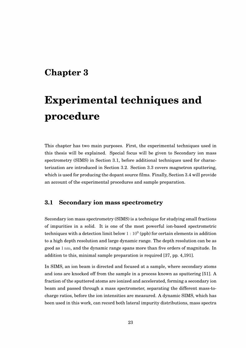
In SIMS, an ion beam is directed and focused at a sample, where secondary atoms
and ions are knocked off from the sample in a process known as sputtering [51]. A
fraction of the sputtered atoms are ionized and accelerated, forming a secondary ion
beam and passed through a mass spectrometer, separating the different mass-to-
charge ratios, before the ion intensities are measured. A dynamic SIMS, which has
been used in this work, can record both lateral impurity distributions, mass spectra
23
Chapter 3. Experimental techniques and procedures 24
S+
FIGURE 3.1: Illustration showing the different parts of the SIMS.
and impurity depth profiles. A schematic illustration of the operating principle is
shown in Figure 3.1.
The following paragraphs will follow Heide’s approach [37].
3.1.1 Principles of sputtering
SIMS utilizes a sputtering1 phenomenon. The ion beam hits the substrate, creating
secondary ions in a two-step process involving sputtering and charge transfer. The
most common type of sputtering is kinetic sputtering, which is a kinematic process
where the kinetic energy from the incoming ion alone is responsible for kicking out
atoms from the surface. One incoming ion may knock off several surface atoms,
and the collisions are thus known as collision cascades. The formation/survival of
charged atoms i.e., ions, after they are sputtered are less understood, but it involves
charge transfer between the atom and the sputtered surface.
Sputtering is characterized by the sputter rate and the sputter yield. The sputter
rate, R, is the rate at which the material is removed from the substrate. The sputter
yield, Y , which is closely related to the sputter rate, is the rate of removal of a
specific atom. The sputter yield will depend on the energy of the incoming species,
the angle and the material examined and varies from element to element. Only
a fraction (∼ 1%) of the sputtered atoms become ionized, and this fraction will be
determined by the ionization yield.1Sputtering is a process in which a solid is bombarded with particles with high energy. The bom-
bardment leads to ejection of particles from the solid.
Chapter 3. Experimental techniques and procedures 25
The sputter and ionization yields will also depend on the host structure, or the
matrix. This is termed matrix effects, and is one of the reasons for the difficulties in
quantifying secondary ion signals, which will be further discussed in Section 3.1.2.
Matrix effects are due to the charge transfer process mentioned above, which is
highly sensitive to the chemistry of the substrate shortly after the sputtering event.
In addition to the effects from the matrix, all elements present in a substrate with
a concentration greater than 1 atm. % will induce their own effects [37, p. 140],
further complicating the quantification [52–54]. Fortunately, the challenge of the
sputter yield may be circumvented by using a reference sample for calibration. This
will be further explained in Section 3.1.2.
Although SIMS is a powerful technique, it is not without drawbacks. Sputtering
is inherently destructive to the sample measured. In addition to this, the sput-
tering process dissipates a significant amount of kinetic energy into the substrate
via nuclear collisions and electronic excitation. The energy induces several other
processes which can modify the composition. These include recoil implantation, cas-
cade mixing, diffusion and segregation. Sputtering can also cause amorphization,
re-crystallization and surface roughening.
3.1.2 Analysis
Once the secondary ions are released, they pass through the electrostatic energy
analyser (EEA) and the magnetic sector analyser (MSA), as shown in Figure 3.1 on
page 24, before they reach the detectors. These two analysers separate the different
masses, first by acting as an energy filter (EEA), then as a mass filter (MSA). The
energy filter alters the direction of the particles so that there is no line of sight
between the sample and the detector. This ensures that neutral species that are
unaffected by the magnetic and electrostatic fields are filtered out. In addition to
this, large ionized molecules will be filtered out, as they will usually have a low
kinetic energy compared to the ions.
The relationship between the mass to charge ratio,m
q, and the electric and mag-
netic fields is derived from the equation for a force exerted on an ion in an electric
field, F = qE, and the equation for an ion in a magnetic field, F = qvmB. Realizing
that the ion will move in a circular path through both analysers, F =mv2
ris used,
giving the formulas
qE =mv2ere
qB =mvmrm
(3.1)
Chapter 3. Experimental techniques and procedures 26
If it is assumed that no energy is lost when the ion travels, vm = ve, and the equa-
tion may be written as:
v2e =qErem
=q2B2r2mm2
(3.2)
Rearranging this with the mass to charge ratio, m/q on the left-hand side, the
equation reads:m
q=
(rmB)2
reE(3.3)
The incoming ions are subjected to an electric and a magnetic field, which can be
adjusted to let through only a specific mass-to-charge ratio.
In practice, as the ions can be both elemental and molecular ions, several different
species will have approximately the same mass. This leads to mass interference.
Mass interference can be resolved either by choosing isotopes that will rarely inter-
fere with others, or by using a high sample voltage offset or a high mass resolution( m
∆m
)setting. However, a high mass resolution is seldom used as it reduces the
intensity, resulting in a higher detection limit.
Once the ions have been detected, the recorded signal can be related to the compo-
sition of the substrate through the formula
Ii = IPY γiAeffTCi (3.4)
Here, Ii is the recorded intensity of element i, IP is the primary beam intensity,
Y is the sputtering yield discussed in Section 3.3, γi is the ionization probability,
Aeff is the analysed area, T is an instrument transmission function and Ci is the
concentration of the element. It is this last factor, Ci which is the quantity that
must be determined by calibration [37]. However, this formula is not used for cal-
ibration due to the difficulty in quantifying the ionization probability, γi. This is a
stochastic variable for which there is no reliable model so far, and although it can
be estimated, the resulting concentration will have a large uncertainty.
Instead, a different approach can be taken in which a reference sample with a
known dose is used for calibration. This sample has been created by ion implanta-
tion to ensure control over the dose. The reference sample is measured under the
same conditions as the sample for which the concentration needs to be calibrated.
The craters of both samples are also measured using a stylus profilometer. This
Chapter 3. Experimental techniques and procedures 27
information allows us to calculate the response function between the actual con-
centration in the sample and the recorded intensity since the concentration of the
reference sample is known.
There are two ways to calculate this response function. If the matrix signal is taken
into account, the response function is called the relative sensitivity factor (RSF) and
is given as
Ci = RSFi ×IiIm
(3.5)
where Im is the measured matrix intensity and the subscript i indicates that the
RSF is only computed for the impurity i.
If the matrix intensity is stable, it can be assumed that it is incorporated in the
response function. This factor is simply called the sensitivity factor (SF). The con-
centration is thus given as
Ci = SFi × Ii (3.6)
If equations 3.4 and 3.6 are combined, an expression for SF as a function of the
different parameters for SIMS is obtained:
SFi =1
IPY γiAeffT(3.7)
Since the SF depends on γi, one reference sample is needed for every element that
will be calibrated unless the same ionization probability is assumed for two ele-
ments. This methods depends on the sample and the reference sample being simi-lar enough so that the SF is the same in both cases, i.e., the matrix effects must be
the same in both cases.
Another potential source of error in SIMS is a memory effect. A memory effect is a
cross-contamination with respect to time, and can occur if a sample has a high con-
centration of a dopant. Parts of the neutral, sputtered atoms will not pass through
the secondary beam line to the detectors but will be deposited on the immersion
lens. These atoms can later be dislodged and ionized, and then accelerated towards
a detector where they are collected. The measured signal will not correspond to the
measured crater only, but is a memory of what was measured previously [55]. The
memory effect can also happen between samples, i.e., Si in ZnO cannot be reliably
measured directly after a run of Si-substrates.
Chapter 3. Experimental techniques and procedures 28
3.1.3 Instrumentation
The instrument used in this work is a Cameca IMS-7f microanalyser. It is equipped
with both a duoplasmatron O +2 -source and a Cs+-source 2. The instrument has both
an electrostatic sector analyser and a magnetic sector analyser, as well as three de-
tectors, namely a Faraday cup, an electron multiplier and a fluorescent screen. The
components are shown in figure 3.1. The SIMS is also equipped with an electron
gun which can be used to bombard the substrate with electrons. This is done to
avoid charge build-up from the continuous primary beam and allow measurements
on high-resistive samples and thin dielectric films.
The Cameca IMS-7f is a combined scanning ion microprobing and ion microscope
instrument, which means that data can be collected in either direct mode (ion mi-
croscope), where the primary beam hits one spot, or in raster mode (scanning ion
microprobing), where the beam is rastered over a quadratic area with sides ranging
from 50 µm to 500 µm.
Ultra-high vacuum is neccessary for SIMS measurements, and the base pressure
in the sample chamber must be .1× 10−9 Torr to ensure a long enough mean free
path for the ions to travel to the detector. The vacuum also controls the rate of de-
position of impurities on the substrate surface, thus a good vacuum may participate
in preventing unnecessary contamination of the sample.
3.2 Other experimental techniques used for character-ization
3.2.1 X-ray diffractometry
X-ray diffractometry (XRD) is a spectroscopic technique for determining the crystal
structure of a material. XRD is based on Bragg’s Law, which tells us that
nλ = 2d sin θ (3.8)
This law is illustrated graphically in Figure 3.2 on page 29. Here, λ is the wave-
length of an incoming beam, while θ is the angle between the incoming beam and
the lattice planes. d is the distance between two lattice planes, so that 2d sin θ is
the extra distance travelled by the incoming beam hitting the lower lattice plane.2Not used in this work.

Chapter 3. Experimental techniques and procedures 29
FIGURE 3.2: Bragg’s law shown graphically.
When this distance is equal to an integer number of wavelengths, there is construc-
tive interference between the two beams, and a signal can be detected.
In XRD, a high-energy monochromatic beam is used to examine a polycrystalline
specimen. By varying the incident angle of the beam, a spectrum of diffraction
intensities versus the angle between the incident beam and the diffraction beam
is recorded. Each intensity corresponds to a certain crystal plane [56, p. 62]. The
Miller indices of these planes can then be found from the formula
sin2 θ =λ2
4a2(h2 + k2 + l2). (3.9)
[56, p. 53]
XRD has been used to investigate the quality of the deposited films and changes in
the films after annealing. The XRD measurements were performed using a Bruker
AXS D8 Discover with a Cu X-ray source. The source has two characteristic peaks
with wavelengths kα1 =1.5406 Å and kα2 =1.5444 Å. A Göbel mirror is implemented
to filter out the kα2-signal. In the measurements, the Bragg-Brentano θ − 2θ or the
2θ − ω-setup was used depending on the flatness of the sample.
3.2.2 Energy dispersive spectroscopy
Energy dispersive spectroscopy (EDS) is a spectroscopic technique measuring char-
acteristic X-rays to identify chemical elements. These X-rays are generated when
Chapter 3. Experimental techniques and procedures 30
an atom is hit by a high-energy particle (electron, photon, ion or neutron). The
particle strikes an electron in an inner shell, knocking it out and thus ionizing
the atom. The vacant electron state is filled with an electron from an outer shell.
The energy difference between the shells will generate either a characteristic X-ray
photon or another characteristic free electron called an Auger electron. In EDS,
the elemental composition is derived from the energy of each characteristic X-ray
photon [56, pp. 191-192].
Unlike X-ray fluorescence spetrometry (XRF), which is a standalone equipment
for elemental analysis, EDS is usually done with an electronic microanalyser inte-
grated with an electron microscope, analyzing X-rays created by the electron beam.
EDS was used to estimate the amount of dopants in the thin film. The EDS mea-
surements were done using a Hitachi TM3000 scanning electron microscope with
a Bruker Quantax 70 energy dispersive X-ray spectrometer. The instrument was
used in the analytic mode, with a high-energy electron beam of 15 keV and a work-
ing distance of 5.5 mm for the ZnO samples and 8.1 mm to 8.3 mm for the GZO sam-
ples (see Section 3.4.1 for sample definition).
3.2.3 Photoluminescence spectroscopy
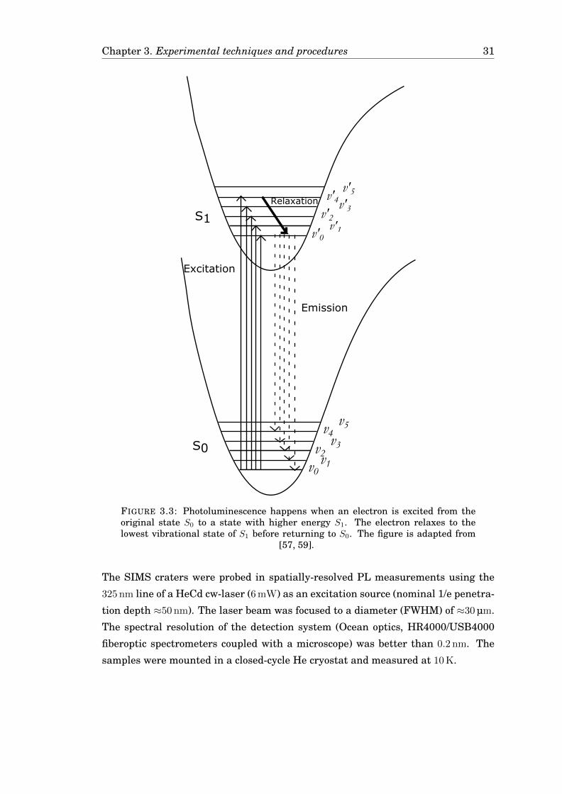
Photoluminescence is the radiation emitted from a molecule or a solid that has
absorbed photon energy from an external source [57, p. 151]. The absorbed energy
excites an electron from the original state (S0) to an energy state with higher energy
(S1). The electron relaxes to the lowest vibrational state of S1, v′0, before returning
to S0, emitting the energy difference as phonons or a photon as shown in Figure 3.3
on page 31. If the energy is lost as phonons, the transition is labelled non-radiative.
Otherwise, a photon is emitted and the process is labelled radiative.
Photoluminescence (PL) spectroscopy is a non-destructive technique using photo-
luminescence spectra to characterize materials. Since all solids exhibit a charac-
teristic set of energy levels, PL can be used to identify a solid. For semiconductors,
a particularly useful feature is the ability to measure the bandgap. Moreover, as
radiative decay in semiconductors often will involve impurity levels, PL can also
be used to reveal spectral peaks corresponding to specific impurities. Finally, it
can also be used to identify surface structures, excited states and recombination
mechanisms [58]. The depth resolution is determined by the absorption coefficient
of the material as well as the intensity of the beam, and is of the order ∼100 nm.
To fully complement the information from a dynamic SIMS, several craters can be
sputtered to different depths in which PL-measurements can then be performed.
Chapter 3. Experimental techniques and procedures 31
v1v0
v2v3
v4v5
v'1v'0
v'2
v'3v'4v'5
S0
S1
Relaxation
Excitation
Emission
FIGURE 3.3: Photoluminescence happens when an electron is excited from theoriginal state S0 to a state with higher energy S1. The electron relaxes to thelowest vibrational state of S1 before returning to S0. The figure is adapted from
[57, 59].
The SIMS craters were probed in spatially-resolved PL measurements using the
325 nm line of a HeCd cw-laser (6 mW) as an excitation source (nominal 1/e penetra-
tion depth ≈50 nm). The laser beam was focused to a diameter (FWHM) of ≈30 µm.
The spectral resolution of the detection system (Ocean optics, HR4000/USB4000
fiberoptic spectrometers coupled with a microscope) was better than 0.2 nm. The
samples were mounted in a closed-cycle He cryostat and measured at 10 K.
Chapter 3. Experimental techniques and procedures 32
3.2.4 Scanning spreading resistance microscopy
Scanning spreading resistance microscopy (SSRM) is a microscopic technique based
on a scanning probe microscope (SPM). The most common SPM-technique is atomic
force microscopy (AFM), where a probe attached to a cantilever is used to measure
topographic features of a surface. When the probe is scanning an area, any varia-
tion in the surface will induce a change in the near-field forces between the atoms in
the tip and the sample, which can change the angle of the cantilever. This angle can
then be measured and used to quantify the topographic differences in the surface
[56, p. 163]. SSRM builds on this technique by using a conductive probe in contact
with the material during a scan, while a DC voltage is applied between a back con-
tact and the probe tip [60, p. 57]. The force between the conductive probe and the
material is normally high to ensure a good electric contact. Since the contact area
is small, the spreading resistance dominates the measurement. This can result in
damage to the sample and probe, which can be a drawback with this method.
SSRM measures resistance to determine carrier concentration in 2D, and is typi-
cally used for measuring cross-sections of doped samples. The ability to measure
two-dimensional profiles combined with a spatial resolution of 1-3 nm and a dy-
namic range from 1× 10¹⁴ carriers/cm3 to 1× 10²¹ carriers/cm3 makes it an excel-
lent technique for characterization of semiconducting materials and devices, par-
ticularly in conjunction with other techniques with a large dynamic range such as
SIMS.
The SSRM measurements were done using a Bruker Dimension 3100 microscope
with a Nanoscope IIIA controller and the Nanoscope 5.33 software. The sensor used
was a Nanosensors CDT-NCHR probe. For the measurement, an area of 4 µm×4 µm was measured, using 128 points in the x-direction and 128 lines in the y-
direction. The scan was done using a ’velocity’ of 0.25 lines/s and the bias-voltage
applied between the back contact and the probe tip was 500 mV.
3.3 Magnetron sputter deposition
Sputtering has already been discussed in Section 3.1.1, in the context of ion beam
sputtering a crater in a sample. However, sputtering can also be used for deposit-
ing thin films. Due to good step coverage, little radiation damage and ability to
produce layers of compound materials and alloys, sputter deposition is a widely
used technique [27, p. 351].
Chapter 3. Experimental techniques and procedures 33
Sputter deposition is done in a vacuum chamber. An inert gas, usually Ar, is led
into the pre-evacuated chamber, in which the base pressure is ∼7.5× 10⁻⁷ Torr.
This gives a working pressure of ∼75 mTorr. To form a plasma, electrons and ions
must be present in the gas. This can be ensured by using a W-igniter. By applying
a voltage across the target and the substrate, the electrons and ions will be acceler-
ated. The positively charged ions in the plasma are accelerated towards the target,
which acts as the cathode. When these ions strike the target, sputtered atoms will
be emitted. Many of these will travel towards the substrate, adsorb and form a
thin-film.
In addition to emitting sputtered atoms, secondary electrons are also emitted. They
will quickly be accelerated away from the target, where they may meet and collide
with Ar-atoms. At sufficiently high energies, the atoms will be ionized by the sec-
ondary electrons and accelerated towards the target, thus sustaining the process of
sputter deposition.
The ion densities in sputtering systems are normally 0.001 %. To increase this, a
magnetic field is applied, causing the secondary electrons to spiral. This lengthens
their path from the cathode to the anode, increasing the probability of ionizing
an atom. The use of magnetic fields in sputter deposition is done by using fixed
bar magnets, and the process is called magnetron sputtering. Magnetron sputter
deposition can bring the ion densities up to 0.03% [27, p. 357].
The Semicore Tri-Axis balanced field magnetron sputter deposition system has
been used in this work to deposit Ag- and Cu-doped ZnO films on ZnO-bulk sub-
strate. The targets used were a 99.99 % pure ZnO-target, 99.999 % pure Ag and
99.999 % pure Cu3. The distance between the targets and substrate was kept at
≈11 cm.
3.4 Experimental procedures
3.4.1 Samples and methodology
Two different ZnO bulk wafers have been investigated in this work. For the un-
doped ZnO, one commercially available wafer from Tokyo Denpa (GZ 0181 1) was
used. The wafer was grown hydrothermally as explained in Section 2.4.1 and cut
perpendicular to the c-axis to a 20 mm× 20 mm× 0.525 mm sample size. The bulk3The purity for Cu and Ag are both qualified guesses based on the usual purity of metal targets.
This was neccessary because the targets were old and the purity no longer known.
Chapter 3. Experimental techniques and procedures 34
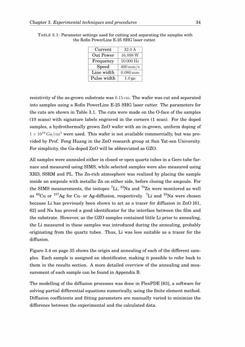
TABLE 3.1: Parameter settings used for cutting and separating the samples withthe Rofin PowerLine E-25 SHG laser cutter.
Current 32.0 A
Out Power 16.898 W
Frequency 50 000 Hz
Speed 400 mm/s
Line width 0.080 mm
Pulse width 1.0 µs
resistivity of the as-grown substrate was 0.15 cm. The wafer was cut and separated
into samples using a Rofin PowerLine E-25 SHG laser cutter. The parameters for
the cuts are shown in Table 3.1. The cuts were made on the O-face of the samples
(10 scans) with signature labels engraved in the corners (1 scan). For the doped
samples, a hydrothermally grown ZnO wafer with an in-grown, uniform doping of
1× 10¹⁹ Ga/cm3 were used. This wafer is not available commercially, but was pro-
vided by Prof. Feng Huang in the ZnO research group at Sun Yat-sen University.
For simplicity, the Ga-doped ZnO will be abbreviated as GZO.
All samples were annealed either in closed or open quartz tubes in a Gero tube fur-
nace and measured using SIMS, while selected samples were also measured using
XRD, SSRM and PL. The Zn-rich atmosphere was realized by placing the sample
inside an ampoule with metallic Zn on either side, before closing the ampoule. For
the SIMS measurements, the isotopes 7Li, 23Na and 70Zn were monitored as well
as 63Cu or 107Ag for Cu- or Ag-diffusion, respectively. 7Li and 23Na were chosen
because Li has previously been shown to act as a tracer for diffusion in ZnO [61,
62] and Na has proved a good identificator for the interface between the film and
the substrate. However, as the GZO samples contained little Li prior to annealing,
the Li measured in these samples was introduced during the annealing, probably
originating from the quartz tubes. Thus, Li was less suitable as a tracer for the
diffusion.
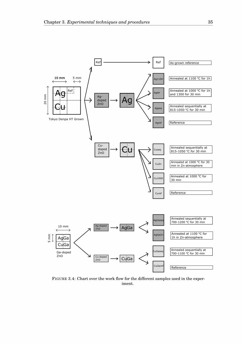
Figure 3.4 on page 35 shows the origin and annealing of each of the different sam-
ples. Each sample is assigned an identificator, making it possible to refer back to
them in the results section. A more detailed overview of the annealing and mea-
surement of each sample can be found in Appendix B.
The modelling of the diffusion processes was done in FlexPDE [63], a software for
solving partial differential equations numerically, using the finite element method.
Diffusion coefficients and fitting parameters are manually varied to minimize the
difference between the experimental and the calculated data.
Chapter 3. Experimental techniques and procedures 35
Annealed at 1100 oC for 1h
Ga-doped
ZnO
Ag-
doped
ZnO
Cu-
doped
ZnO
Ag1100
Annealed sequentially at
815-1050 oC for 30 min
Annealed at 1000 oC for 1h
and 1300 for 30 min
Reference
Reference
Annealed at 1000 oC for
30 min
Annealed at 1000 oC for 30
min in Zn-atmosphere
As-grown referenceRef
Ag-doped
ZnO10 mm
5 m
m
Annealed sequentially at
700-1100 oC for 30 min
Annealed sequentially at
700-1200 oC for 30 min
Reference
Annealed sequentially at
815-1050 oC for 30 min
Annealed at 1100 oC for
1h in Zn-atmosphere
Ag
Cu
Tokyo Denpa HT Grown
10 mm
20 m
m
10 mm 5 mm
Ref
Ref
Agdir
Agseq
Agref
Cuseq
CuZn
Cu1000
Curef
Cu
AgGa
CuGa
AgGa
AgGaseq
AgGaZn
Cu-doped
ZnO CuGa
CuGaseq
CuGaref
FIGURE 3.4: Chart over the work flow for the different samples used in the exper-iment.
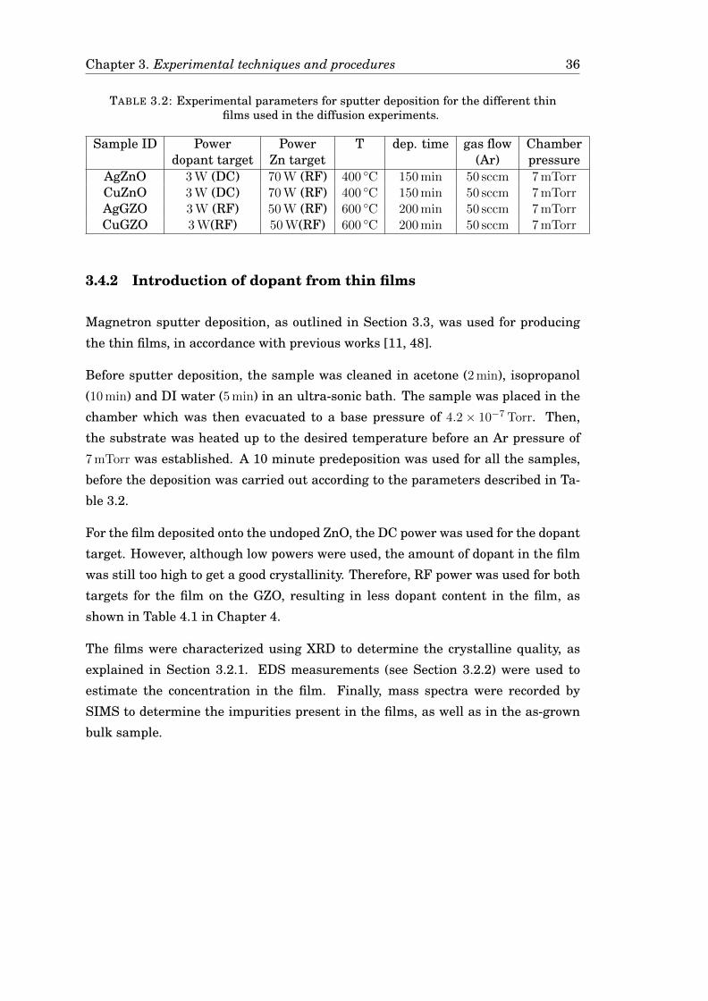
Chapter 3. Experimental techniques and procedures 36
TABLE 3.2: Experimental parameters for sputter deposition for the different thinfilms used in the diffusion experiments.
Sample ID Power Power T dep. time gas flow Chamberdopant target Zn target (Ar) pressure
AgZnO 3 W (DC) 70 W (RF) 400 C 150 min 50 sccm 7 mTorrCuZnO 3 W (DC) 70 W (RF) 400 C 150 min 50 sccm 7 mTorrAgGZO 3 W (RF) 50 W (RF) 600 C 200 min 50 sccm 7 mTorrCuGZO 3 W(RF) 50 W(RF) 600 C 200 min 50 sccm 7 mTorr
3.4.2 Introduction of dopant from thin films
Magnetron sputter deposition, as outlined in Section 3.3, was used for producing
the thin films, in accordance with previous works [11, 48].
Before sputter deposition, the sample was cleaned in acetone (2 min), isopropanol
(10 min) and DI water (5 min) in an ultra-sonic bath. The sample was placed in the
chamber which was then evacuated to a base pressure of 4.2× 10⁻⁷ Torr. Then,
the substrate was heated up to the desired temperature before an Ar pressure of
7 mTorr was established. A 10 minute predeposition was used for all the samples,
before the deposition was carried out according to the parameters described in Ta-
ble 3.2.
For the film deposited onto the undoped ZnO, the DC power was used for the dopant
target. However, although low powers were used, the amount of dopant in the film
was still too high to get a good crystallinity. Therefore, RF power was used for both
targets for the film on the GZO, resulting in less dopant content in the film, as
shown in Table 4.1 in Chapter 4.
The films were characterized using XRD to determine the crystalline quality, as
explained in Section 3.2.1. EDS measurements (see Section 3.2.2) were used to
estimate the concentration in the film. Finally, mass spectra were recorded by
SIMS to determine the impurities present in the films, as well as in the as-grown
bulk sample.
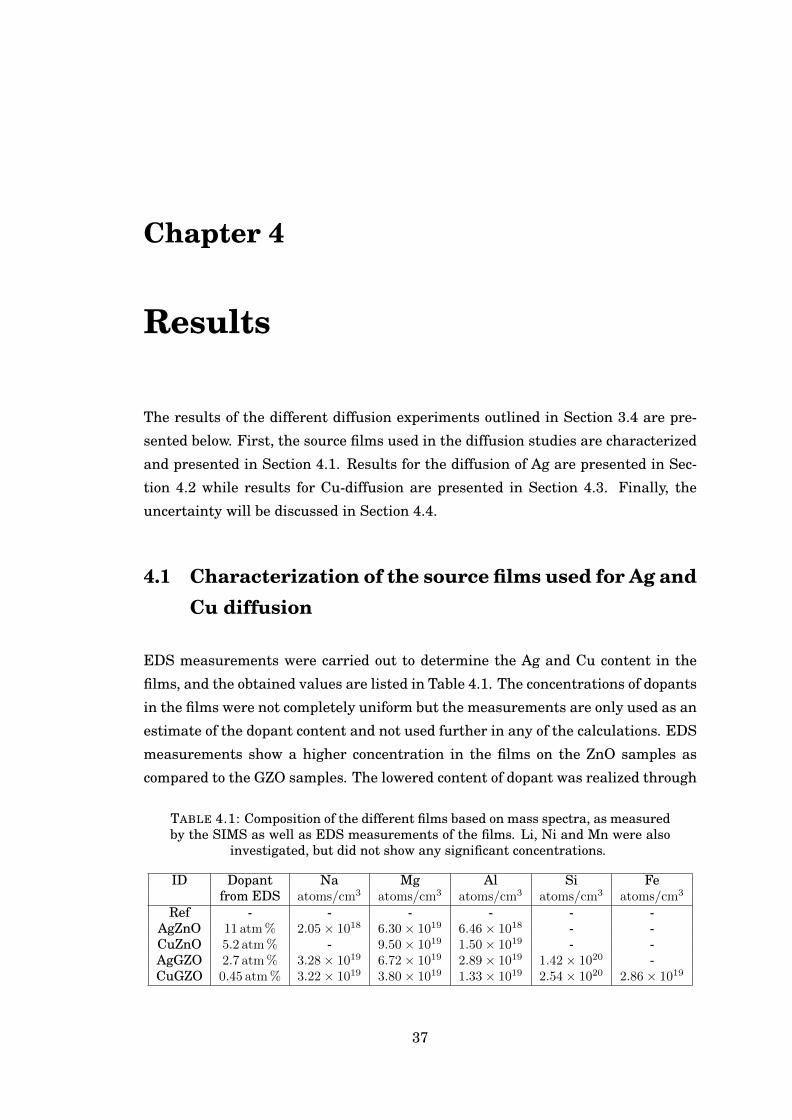
Chapter 4
Results
The results of the different diffusion experiments outlined in Section 3.4 are pre-
sented below. First, the source films used in the diffusion studies are characterized
and presented in Section 4.1. Results for the diffusion of Ag are presented in Sec-
tion 4.2 while results for Cu-diffusion are presented in Section 4.3. Finally, the
uncertainty will be discussed in Section 4.4.
4.1 Characterization of the source films used for Ag andCu diffusion
EDS measurements were carried out to determine the Ag and Cu content in the
films, and the obtained values are listed in Table 4.1. The concentrations of dopants
in the films were not completely uniform but the measurements are only used as an
estimate of the dopant content and not used further in any of the calculations. EDS
measurements show a higher concentration in the films on the ZnO samples as
compared to the GZO samples. The lowered content of dopant was realized through
TABLE 4.1: Composition of the different films based on mass spectra, as measuredby the SIMS as well as EDS measurements of the films. Li, Ni and Mn were also
investigated, but did not show any significant concentrations.
ID Dopant Na Mg Al Si Fefrom EDS atoms/cm3 atoms/cm3 atoms/cm3 atoms/cm3 atoms/cm3
Ref - - - - - -AgZnO 11 atm % 2.05× 10¹⁸ 6.30× 10¹⁹ 6.46× 10¹⁸ - -CuZnO 5.2 atm % - 9.50× 10¹⁹ 1.50× 10¹⁹ - -AgGZO 2.7 atm % 3.28× 10¹⁹ 6.72× 10¹⁹ 2.89× 10¹⁹ 1.42× 10²⁰ -CuGZO 0.45 atm % 3.22× 10¹⁹ 3.80× 10¹⁹ 1.33× 10¹⁹ 2.54× 10²⁰ 2.86× 10¹⁹
37
Chapter 4. Results 38
using an RF voltage on the dopant target instead of a DC voltage to reduce the
sputter rate.
XRD measurements showed that both the Ag-doped film on ZnO and on GZO con-
tained Ag-precipitate. In contrast, the Cu-doped films showed no signs of precipi-
tate.
Mass spectra of all the films as well as the as-grown reference sample were aquired
using SIMS and are shown in Figure 4.1. These measurements were not calibrated,
so depending on the ionization probability of an impurity, the intensity could vary.
All measurements were done under the same conditions on the same day, so that
the impurity intensities were comparable between the different samples. The im-
purity concentrations for some of the impurities are shown in Table 4.1. Only the
Na-reference was measured with the samples. The concentrations of the other im-
purities were deduced using previous reference measurements to convert between
different sensitivy factors (see Section 3.1.2) under the assumption that the rela-
tionship between the different sensitivity factors under a given set of experimental
conditions are constant, i.e.,
SFXnew = SFXpreviousSFNanew
SFNaprevious
(4.1)
Thus, the uncertainty in these measurements will be closer to 20 - 30 %, as opposed
to 10 % for a calibrated SIMS measurement. It was also noticed that there are
more impurities in the thin films deposited on the GZO wafers compared to the
films deposited on the ZnO wafers.
4.2 Diffusion of Ag
Diffusion of Ag was studied in both undoped and Ga-doped HT-grown ZnO, as out-
lined in Section 3.4.
4.2.1 Diffusion of Ag in undoped ZnO
The concentration vs. depth-profiles for an Ag-doped ZnO film on a ZnO substrate
(sample Agseq) are shown in Figure 4.2 on page 39. The sample was annealed at
temperatures between 815 C and 1000 C as outlined in Section 3.4.
The Ag concentration profiles in Figure 4.2 on page 39 show flat or very slowly
decaying profiles of Ag with a sharp interface between the concentration in the film

Chapter 4. Results 39
10 20 30 40 50 60 70 80 90 100 110 120
1000
10000
as-grown ZnO
AgZnO
CuZnO
AgGZO
CuGZO
NaMg
Mg
Si
Al
Al
Al
AlO
O
O
O S
S
S
S KCa
Cu
Zn
Zn
Zn
Zn
Se
Rb
Se
CaKS
SiMgNaO
Ag
CuZn
Mass (a.m.u)
Inte
nsity
(cou
nts/
s)
Sample
s
Ag
Rb
NaMg
FIGURE 4.1: Mass spectra showing the chemical composition of the different filmsand the as-grown ZnO. Concentrations of some impurities are given in Table 4.1
0 2 4 6
1E17
1E18
1E19
1E20
1E21
1E22
107 A
g co
ncen
tratio
n (a
tom
s/cm
3 )
Depth (um)
as-deposited 815 oC 900 oC 950 oC1000 oC
FIGURE 4.2: Concentration profiles of Ag in ZnO for temperatures from 815 C to1000 C (sample Agseq). . The measured isotope is 107Ag, which accounts for 52 %
of the total silver amount.
Chapter 4. Results 40
and the bulk. A small increase in the concentration below the source layer can be
seen in some of the profiles. However, the lack of coherent results, e.g., a decrease
in concentration from 950 C to 1000 C, indicates a different origin than diffusion.
From measurements done using EDS (Table 4.1), it was clear that the concentra-
tion of Ag in the film was very high. A memory effect was therefore suspected and
investigated through a series of measurements shown together in Figure 4.3b on
page 41. In order to eliminate this effect, a crater with sides of 250 µm was sput-
tered through the Ag-film. Then, a pre-sputtering was performed on a Si-sample
not containing any significant amount of Ag, in order to cover the immersion lens
with traces of Si instead of Ag. After a few minutes of pre-sputtering, the beam
was moved back to the Ag-sample and another, smaller crater with sides of 150 µm
was sputtered as shown in Figure 4.3a. From these measurements it was estab-
lished that the apparent profile was most likely a memory effect due to the high
Ag content in the film, and there was no indication of diffusion at concentrations
higher than 1× 10¹⁶ atoms/cm3 for this temperature range. However, as the refer-
ence sample from Figure 4.3b shows1, a diffusion could very well happen at lower
concentrations, only becoming visible when the impurities are trapped at a concen-
tration above the detection limit.
The annealing temperature was increased further, and at 1300 C, a diffusion profile
was observed in sample Agdir, see Figure 4.4. However, the sample was also heavily
degraded and almost all of the Ag-doped film evaporated, so no further annealing
was performed.
Since the sample was treated at a high temperature in a quartz tube, additional
impurities may have been introduced during the annealing, creating a trap for the
migrating Ag. The sample was therefore investigated by SIMS to see if a likely im-
purity was present. However, no plausible candidate was found among the species
studied in the region of interest. The results along with additional remarks are
found in Appendix C.
4.2.2 Diffusion of Ag in Ga-doped ZnO
Figure 4.5 on page 43 shows the concentration vs. depth-profiles for sample Ag-Gaseq, i.e., Ag-doped ZnO on a ZnO substrate doped uniformally with 1× 10¹⁹ Ga/cm3
(GZO). The sample was annealed at temperatures from 700 C to 1200 C. Diffusion
is evident at temperatures above 1000 C, appearing as a monotonically decreasing1The reference sample may seem peculiar, but due to problems with high resistivity in the Ag
reference sample, an annealed sample was used for the reference measurement.
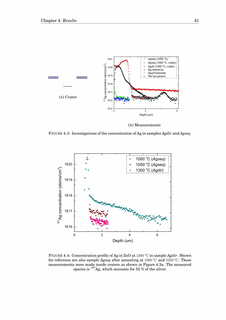
Chapter 4. Results 41
(A) Crater
0 2 4
Depth (um)
Agseq (1000 oC) Agseq (1000 oC, crater) Agdir (1000 oC, crater) Ag-reference Agref backside Ref (as-grown)
1E15
1E16
1E17
1E18
1E19
1E20
1E21
107 A
g co
ncen
tratio
n (a
tom
s/cm
3 )
(B) Measurements
FIGURE 4.3: Investigations of the concentration of Ag in samples Agdir and Agseq.
0 2 4 6
Depth (um)
1E16
1E17
1E18
1E19
1E20 1000 oC (Agseq) 1050 oC (Agseq) 1300 oC (Agdir)
107 A
g co
ncen
tratio
n (a
tom
s/cm
3 )
FIGURE 4.4: Concentration profile of Ag in ZnO at 1300 C in sample Agdir. Shownfor reference are also sample Agseq after annealing at 1000 C and 1050 C. Thesemeasurements were made inside craters as shown in Figure 4.3a. The measured
species is 107Ag, which accounts for 52 % of the silver.
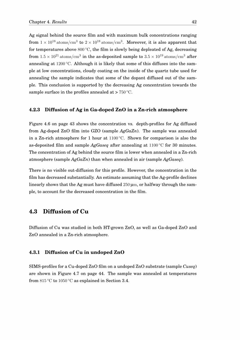
Chapter 4. Results 42
Ag signal behind the source film and with maximum bulk concentrations ranging
from 1× 10¹⁸ atoms/cm3 to 2× 10¹⁸ atoms/cm3. Moreover, it is also apparent that
for temperatures above 800 C, the film is slowly being depleated of Ag, decreasing
from 1.5× 10²¹ atoms/cm3 in the as-deposited sample to 3.5× 10¹⁹ atoms/cm3 after
annealing at 1200 C. Although it is likely that some of this diffuses into the sam-
ple at low concentrations, cloudy coating on the inside of the quartz tube used for
annealing the sample indicates that some of the dopant diffused out of the sam-
ple. This conclusion is supported by the decreasing Ag concentration towards the
sample surface in the profiles annealed at > 750 C.
4.2.3 Diffusion of Ag in Ga-doped ZnO in a Zn-rich atmosphere
Figure 4.6 on page 43 shows the concentration vs. depth-profiles for Ag diffused
from Ag-doped ZnO film into GZO (sample AgGaZn). The sample was annealed
in a Zn-rich atmosphere for 1 hour at 1100 C. Shown for comparison is also the
as-deposited film and sample AgGaseq after annealing at 1100 C for 30 minutes.
The concentration of Ag behind the source film is lower when annealed in a Zn-rich
atmosphere (sample AgGaZn) than when annealed in air (sample AgGaseq).
There is no visible out-diffusion for this profile. However, the concentration in the
film has decreased substantially. An estimate assuming that the Ag-profile declines
linearly shows that the Ag must have diffused 250 µm, or halfway through the sam-
ple, to account for the decreased concentration in the film.
4.3 Diffusion of Cu
Diffusion of Cu was studied in both HT-grown ZnO, as well as Ga-doped ZnO and
ZnO annealed in a Zn-rich atmosphere.
4.3.1 Diffusion of Cu in undoped ZnO
SIMS-profiles for a Cu-doped ZnO film on a undoped ZnO substrate (sample Cuseq)
are shown in Figure 4.7 on page 44. The sample was annealed at temperatures
from 815 C to 1050 C as explained in Section 3.4.
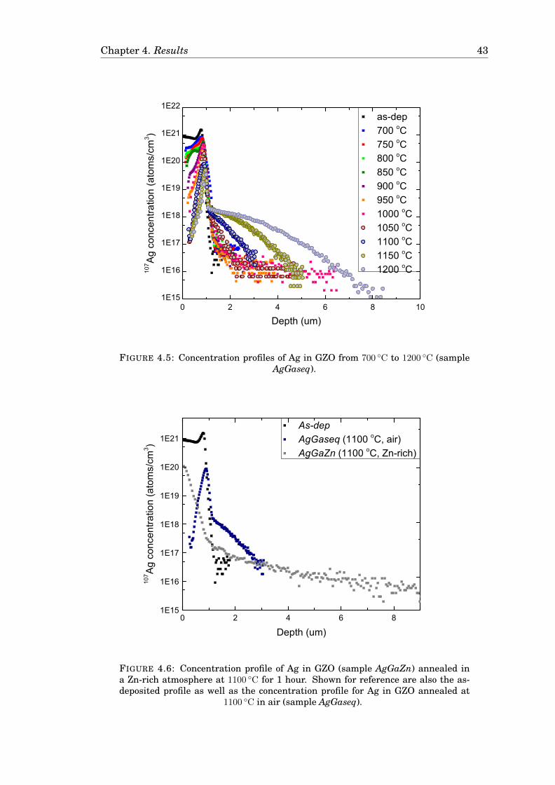
Chapter 4. Results 43
0 2 4 6 8 101E15
1E16
1E17
1E18
1E19
1E20
1E21
1E22
Depth (um)
as-dep 700 oC 750 oC 800 oC 850 oC 900 oC 950 oC 1000 oC 1050 oC 1100 oC 1150 oC 1200 oC10
7 Ag
conc
entra
tion
(ato
ms/
cm3 )
FIGURE 4.5: Concentration profiles of Ag in GZO from 700 C to 1200 C (sampleAgGaseq).
0 2 4 6 8
Depth (um)
1E15
1E16
1E17
1E18
1E19
1E20
1E21 As-dep AgGaseq (1100 oC, air) AgGaZn (1100 oC, Zn-rich)
107 A
g co
ncen
tratio
n (a
tom
s/cm
3 )
FIGURE 4.6: Concentration profile of Ag in GZO (sample AgGaZn) annealed ina Zn-rich atmosphere at 1100 C for 1 hour. Shown for reference are also the as-deposited profile as well as the concentration profile for Ag in GZO annealed at
1100 C in air (sample AgGaseq).
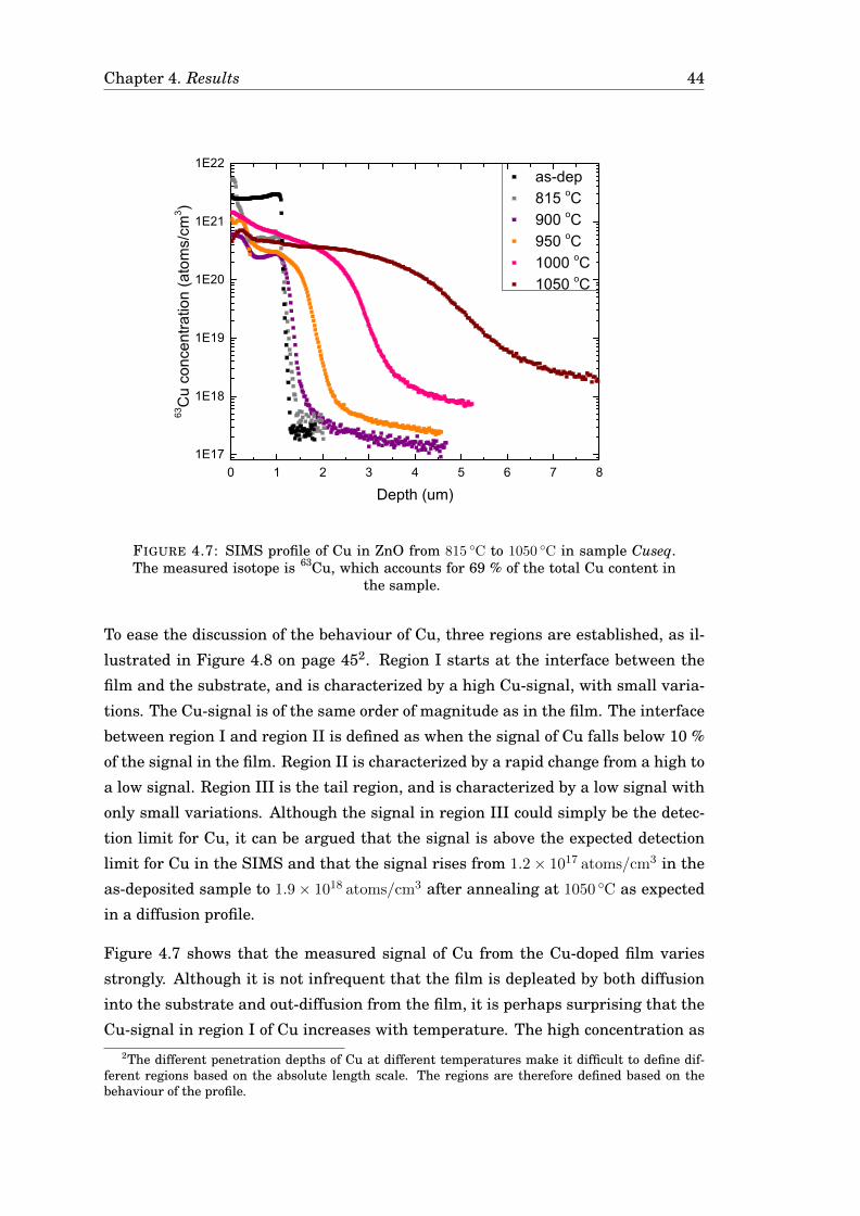
Chapter 4. Results 44
0 1 2 3 4 5 6 7 81E17
1E18
1E19
1E20
1E21
1E22 as-dep 815 oC 900 oC 950 oC 1000 oC 1050 oC
63C
u co
ncen
tratio
n (a
tom
s/cm
3 )
Depth (um)
FIGURE 4.7: SIMS profile of Cu in ZnO from 815 C to 1050 C in sample Cuseq.The measured isotope is 63Cu, which accounts for 69 % of the total Cu content in
the sample.
To ease the discussion of the behaviour of Cu, three regions are established, as il-
lustrated in Figure 4.8 on page 452. Region I starts at the interface between the
film and the substrate, and is characterized by a high Cu-signal, with small varia-
tions. The Cu-signal is of the same order of magnitude as in the film. The interface
between region I and region II is defined as when the signal of Cu falls below 10 %
of the signal in the film. Region II is characterized by a rapid change from a high to
a low signal. Region III is the tail region, and is characterized by a low signal with
only small variations. Although the signal in region III could simply be the detec-
tion limit for Cu, it can be argued that the signal is above the expected detection
limit for Cu in the SIMS and that the signal rises from 1.2× 10¹⁷ atoms/cm3 in the
as-deposited sample to 1.9× 10¹⁸ atoms/cm3 after annealing at 1050 C as expected
in a diffusion profile.
Figure 4.7 shows that the measured signal of Cu from the Cu-doped film varies
strongly. Although it is not infrequent that the film is depleated by both diffusion
into the substrate and out-diffusion from the film, it is perhaps surprising that the
Cu-signal in region I of Cu increases with temperature. The high concentration as2The different penetration depths of Cu at different temperatures make it difficult to define dif-
ferent regions based on the absolute length scale. The regions are therefore defined based on thebehaviour of the profile.

Chapter 4. Results 45
Film Region I Region II Region III
Depth (um)
(ato
ms/c
m3)
FIGURE 4.8: Regions for describing the signal of Cu in ZnO. Region I is the highsignal region, region II is the intermediary region where the signal changes rapidly
and region III is the low signal tail.
0 1 2 3 4 5100
1000
10000
Inte
nsity
of Z
n-si
gnal
(cou
nts/
s)
Depth (um)
as-dep 815 oC 900 oC 950 oC 1000 oC 1050 oC
As-deposited 63Cu-profile
1E17
1E18
1E19
1E20
1E2163
Cu
conc
entra
tion
(ato
ms/
cm3 )
FIGURE 4.9: Zn-signal as a function of depth for the measurements shown inFigure 4.7 on page 44 (sample Cuseq). The signals have been normalized. The
as-deposited profile of Cu is shown to indicate where the film ends.
Chapter 4. Results 46
0 5 10 15 20 25 301E16
1E17
1E18
1E19
1E20
1E21
63C
u co
ncen
tratio
n (a
tom
s/cm
3 )
Depth (um)
FIGURE 4.10: SIMS-profile of Cu:ZnO on ZnO annealed at 1000 C (sampleCu1000). The measured species is 63Cu, which accounts for 69 % of the Cu in
the sample.
well as the nonsystematic variations in concentration point towards an alternative
interpretation of the Cu-signal in region I and II. This will be further discussed
in Chapter 5. This is also supported by changes in the Zn-signal for the same
measurements as shown in Figure 4.9 on page 45.
The behaviour of Cu in region III was also studied separately on sample Cu1000,
which had been annealed once at 1000 C for 30 minutes. Since this sample was
used for PL-measurements (see Section 4.3.4), a crater had already been sputtered
to reach region III. A concentration vs. depth-profile was measured from this crater,
as showed in Figure 4.10. As the dynamic range of the SIMS instrument is five
orders of magnitude, measuring inside the crater ensures that any variations in the
low concentration region can be detected by omitting the memory effect mentioned
above. The measurement showed that the profile is at least 28 µm deep and that it
falls off very slowly.
Chapter 4. Results 47
4.3.2 Diffusion of Cu in Ga-doped ZnO
Figure 4.11 on page 48 shows the SIMS-profile of Cu in Ga-doped ZnO (sample
CuGaseq). The sample was annealed at temperatures from 700 C to 1100 C. Dif-
fusion is observed at temperatures above 800 C. Similar to the profiles for Cu in
ZnO (Section 4.3.1), there is no clear interface between the film and the bulk in the
Cu-signal. However, the similarities are most notable at high concentrations of Cu.
For concentrations of Cu lower than ≈1× 10¹⁹ atoms/cm3, the profile behaves differ-
ently. At this level, there is a distinct change in the derivative of the concentration
profile which is most evident at 850 C, 900 C and 950 C.
4.3.3 Diffusion of Cu in ZnO in a zinc-rich environment
Figure 4.12 shows the SIMS-profile of Cu in undoped ZnO after annealing in a Zn-
rich atmosphere at 1000 C for 30 minutes (Sample CuZn). Also shown for reference
is the as-deposited sample as well as sample Cuseq (sequentially annealed up to
1000 C) and Cu1000 annealed once at 1000 C.
From this figure it is noticeable that a Zn-rich atmosphere changes the resulting
SIMS-profile. The penetration depth is shorter and the concentration of Cu in the
film as well as in all regions is lower in the sample annealed in Zn-rich atmosphere.
The profile also shows a pile-up of Cu approximately 1 µm from the interface be-
tween the bulk and the film. This pile-up is similar to the one seen by Azarov et al.
[23] for diffusion of Agi in ZnO (shown in Figure 2.8 on page 22). This could indicate
a diffusion process at a low concentration where diffusing Cu is trapped, building
up a concentration and creating a visible peak.
4.3.4 Complementary measurements
XRD results for Cu-doped samples
Due to the high concentration of Cu in the samples, XRD measurements were per-
formed at several temperatures.
Figure 4.13 on page 49 shows the diffractogram of sample Cuseq as-deposited, af-
ter annealing at 815 C and after annealing at 1000 C, as well as sample CuZn and
Cu1000, which were both annealed at 1000 C. CuO is present in both sample Cuseqat 815 C and 1000 C, and Cu1000 (annealed in air), but not in sample CuZn (an-
nealed in a Zn-rich atmosphere). Furthermore, there was no evidence of CuO in
Chapter 4. Results 48
0 2 4 6 8 10 12 14 161E15
1E16
1E17
1E18
1E19
1E20
63C
u co
ncen
tratio
n (a
tom
s/cm
3 )
Depth (um)
as-dep 700 oC 750 oC 800 oC 850 oC 900 oC 950 oC 1000 oC 1050 oC 1100 oC
FIGURE 4.11: SIMS-profile of Cu:ZnO on GZO annealed from 700 C to 1100 C insample CuGaseq.
0 1 2 3 4 5 6 71E17
1E18
1E19
1E20
1E21
1E22 as-dep Cuseq (seq. to 1000 oC, air) Cu1000 (1000 oC, air) CuZn (1000 oC, Zn-rich)
63C
u co
ncen
tratio
n (a
tom
s/cm
3 )
Depth (um)
FIGURE 4.12: SIMS-profile of Cu-doped ZnO on ZnO annealed in Zn-rich atmo-sphere at 1000 °C for 30 minutes (sample CuZn), compared to sample Cuseq and
Cu1000, both annealed at 1000 C in air, as well as the as-deposited film.
Chapter 4. Results 49
35 40 45
102104106108102104106108102104106108102104106108
35 40 45
102104106108
Angle
as-dep
CuO:002/111ZnO:1011 CuO:200
ZnO:0002
ZnO:0002
setup
Cuseq (815 oC)
ZnO:1011CuO:111 CuO:200 setup
Inte
nsity Cuseq (1000 oC)unidentified peak
CuO:200ZnO:1011CuO:002/111
setup
Cu1000
Zn:1011ZnO:1011
ZnO:0002
ZnO:0002
setup
ZnO:0002
CuZn
FIGURE 4.13: XRD-measurements of Cu-doped ZnO on ZnO annealed for 30 minat 815 C and 1000 C (samples Cuseq, CuZn and Cu1000). Sample CuZn wasannealed in a Zn-rich atmosphere, while the others were annealed in air. TheMiller indices for CuO, ZnO and Zn refers to the monoclinic crystal, the hexagonal
wurtzite structure and the hexagonal closed-packed structure, respectively.
the sample prior to annealing. Sample CuZn shows a peak that can be attributed
to elemental Zn. This is not surprising as Zn remained on the sample surface after
annealing in a Zn-rich atmosphere. A comparison of the area of the (111)-peak in
Cuseq at 815 C and 1000 C, and Cu1000 indicates that the area of the peak is three
times as large at 815 C and over four times as large in Cu1000 compared to Cuseqannealed at 1000 C. As the area of the XRD-peak is proportional to the volume in
the sample, this points to there being more CuO in the samples with no annealing
history. In Cuseq annealed at 815 C and Cu1000, the (200) peak was also identified,
pointing to even more CuO in these samples.
Results from complementary X-ray photoelectron spectroscopy (XPS) measured on
sample Cuseq annealed to 1000 C showed both CuO and Cu2O. As XPS is a surface
technique, this indicates that Cu2O was found on the surface, but not in detectable
amounts in the bulk, while CuO is present both on the surface and in the bulk. The
XPS-results are presented in Appendix D.
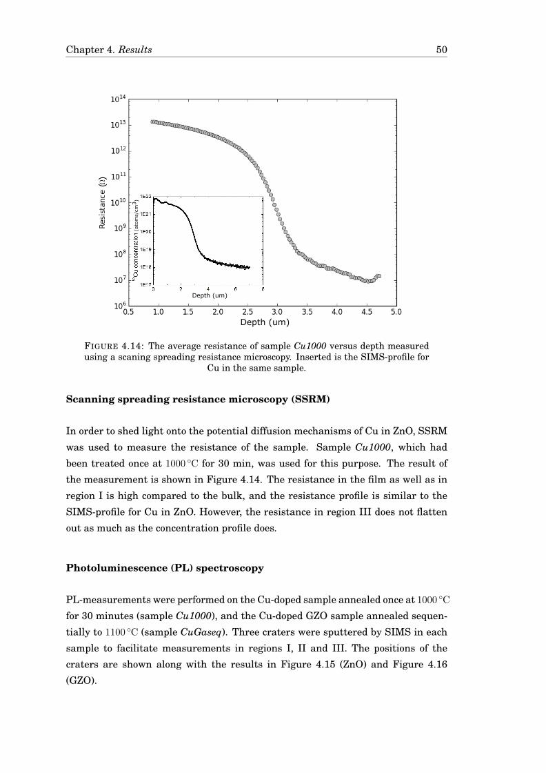
Chapter 4. Results 50
Depth (um)
Depth (um)
(ato
ms/c
m3)
( )
FIGURE 4.14: The average resistance of sample Cu1000 versus depth measuredusing a scaning spreading resistance microscopy. Inserted is the SIMS-profile for
Cu in the same sample.
Scanning spreading resistance microscopy (SSRM)
In order to shed light onto the potential diffusion mechanisms of Cu in ZnO, SSRM
was used to measure the resistance of the sample. Sample Cu1000, which had
been treated once at 1000 C for 30 min, was used for this purpose. The result of
the measurement is shown in Figure 4.14. The resistance in the film as well as in
region I is high compared to the bulk, and the resistance profile is similar to the
SIMS-profile for Cu in ZnO. However, the resistance in region III does not flatten
out as much as the concentration profile does.
Photoluminescence (PL) spectroscopy
PL-measurements were performed on the Cu-doped sample annealed once at 1000 C
for 30 minutes (sample Cu1000), and the Cu-doped GZO sample annealed sequen-
tially to 1100 C (sample CuGaseq). Three craters were sputtered by SIMS in each
sample to facilitate measurements in regions I, II and III. The positions of the
craters are shown along with the results in Figure 4.15 (ZnO) and Figure 4.16
(GZO).
Chapter 4. Results 51
In Figure 4.15b on page 52, the deep and middle signals show an emission peak
near 510 nm. Although this peak could be attributed to several defects, the structure
of the left shoulder of the peak is characteristic of CuZn [64–68]. For the peak from
the shallow crater, no such structure is observed. It is also noticeable that the near-
bandgap emission varies between the samples. If normalized, the signal from the
middle crater is ∼350 times stronger than that from the deep crater. This cannot
be explained solely by the total concentration of Cu.
Figure 4.16b on page 52 differs from Figure 4.15b on several important points. In
GZO, a peak is present at 510 nm for the surface and the shallow crater. However,
the structure of the left shoulder is not present, and it is not clear whether the
peak is attributed to CuZn or not. For the middle crater, a peak is present, but the
maximum of the peak is not at 510 nm. For the deep crater, there is no evidence of a
peak at 510 nm, despite a very strong signal from the near-band emission. Another
peak is present for the deep crater, which has previously been attributed to the Zn-
vacancy [69, 70]. As this was measured in the bulk of GZO where the Fermi level
position is very high, a strong signal from vZn may be anticipated.
4.4 Uncertainty in the measurements
Due to its qualitative and exploratory nature, a complete and rigourous treatment
of the uncertainty and errors is beyond the scope of this work. In general, mea-
surements were performed indicate the existence of a phenomenon, rather than to
quantify it. Possible sources of errors and their significance will nevertheless be
discussed below.
The uncertainty of SIMS-measurements are usually taken to be 10 % and assumes
that the lenses are perfectly lined up, adequate reference samples measured under
the same conditions as the sample and an optimal choice of measurement parame-
ters is found. The uncertainty is an estimate based on the combined uncertainty of
the ion implantation dose in the reference sample, variations in the sputter yield,
statistical variations in the measured signal and uncertainty in the measurement
of the resulting crater with the stylus profilometer.
When reference sample measurements are not performed for every measurement,
or an adequate reference sample is missing, the corresponding concentration must
be computed, and the uncertainty in the measurements increases. Matrix effects,
selective sputtering and memory effects, on the other hand, will constitute system-
atic errors that one should attempt to eliminate. Both matrix and memory effects
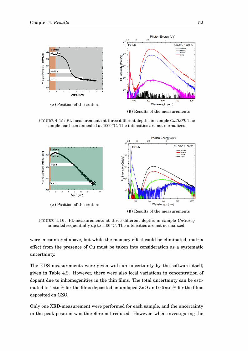
Chapter 4. Results 52
(A) Position of the craters
(B) Results of the measurements
FIGURE 4.15: PL-measurements at three different depths in sample Cu1000. Thesample has been annealed at 1000 C. The intensities are not normalized.
(A) Position of the craters(B) Results of the measurements
FIGURE 4.16: PL-measurements at three different depths in sample CuGaseqannealed sequentially up to 1100 C. The intensities are not normalized.
were encountered above, but while the memory effect could be eliminated, matrix
effect from the presence of Cu must be taken into consideration as a systematic
uncertainty.
The EDS measurements were given with an uncertainty by the software itself,
given in Table 4.2. However, there were also local variations in concentration of
dopant due to inhomogenities in the thin films. The total uncertainty can be esti-
mated to 1 atm% for the films deposited on undoped ZnO and 0.5 atm% for the films
deposited on GZO.
Only one XRD-measurement were performed for each sample, and the uncertainty
in the peak position was therefore not reduced. However, when investigating the
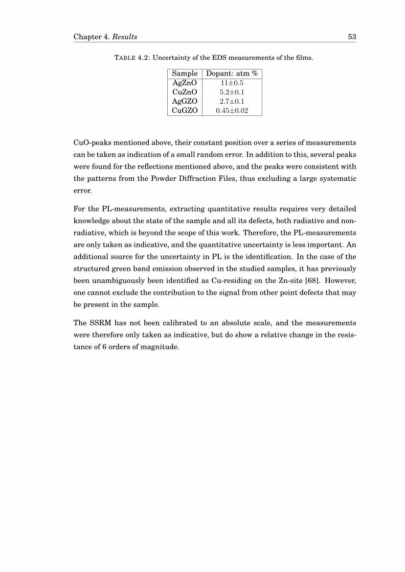
Chapter 4. Results 53
TABLE 4.2: Uncertainty of the EDS measurements of the films.
Sample Dopant: atm %AgZnO 11±0.5CuZnO 5.2±0.1AgGZO 2.7±0.1CuGZO 0.45±0.02
CuO-peaks mentioned above, their constant position over a series of measurements
can be taken as indication of a small random error. In addition to this, several peaks
were found for the reflections mentioned above, and the peaks were consistent with
the patterns from the Powder Diffraction Files, thus excluding a large systematic
error.
For the PL-measurements, extracting quantitative results requires very detailed
knowledge about the state of the sample and all its defects, both radiative and non-
radiative, which is beyond the scope of this work. Therefore, the PL-measurements
are only taken as indicative, and the quantitative uncertainty is less important. An
additional source for the uncertainty in PL is the identification. In the case of the
structured green band emission observed in the studied samples, it has previously
been unambiguously been identified as Cu-residing on the Zn-site [68]. However,
one cannot exclude the contribution to the signal from other point defects that may
be present in the sample.
The SSRM has not been calibrated to an absolute scale, and the measurements
were therefore only taken as indicative, but do show a relative change in the resis-
tance of 6 orders of magnitude.

Chapter 5
Discussion
The results presented in Chapter 4 are discussed below. In Section 5.1, the results
will be summarized and compared. Section 5.2 will discuss indications and impli-
cations of the CuO present. In Section 5.3, a hypothesis for the diffusion of these
two potential p-type dopants will be discussed. This will be further elaborated on
and supported by computational results in Section 5.4. Finally, the model will be
compared to other diffusion experiments in Section 5.5.
5.1 Summary and comparison of results
No diffusion of Ag in undoped ZnO was observed when annealed at temperatures
up to 1050 C. The measurements had a detection limit of ≈1× 10¹⁶ atoms/cm3, so
one cannot exclude diffusion of Ag at lower concentrations. However, at 1300 C
diffusion was observed. In Ga-doped ZnO, diffusion of Ag could be seen for tem-
peratures above 1000 C. Moreover, when Ag in GZO was annealed in a Zn-rich
atmosphere, the solubility of Ag was reduced, resulting in a deep profile at a low
concentration.
Diffusion of Cu was studied in undoped ZnO, GZO and for undoped ZnO after an-
nealing in a Zn-rich atmosphere. In both ZnO and GZO, the concentration of Cu in
region I behind the source film was of the same order of magnitude as the concen-
tration in the film. The diffusion in region III in ZnO showed a diffusion profile for
which the solubility increases with temperature. This diffusion profile was further
investigated and found to be very deep, >28 µm. In GZO, the solubility of Cu was
enhanced and the resulting diffusion profile was readily observed. However, there
was a change happening in GZO after annealing at 1050 C, causing an apparent
55
Chapter 5. Discussion 56
0 1 2 3 4 5 6 7 8 9 10 11 12 13 14 151E16
1E17
1E18
1E19
1E20
107Ag 1000 oC 107Ag 1050 oC 107Ag 1100 oC 63Cu 1000 oC 63Cu1050 oC 63Cu 1100 oC
Con
cent
ratio
n (a
tom
s/cm
3 )
Depth (um)
FIGURE 5.1: Comparison between the diffusion of Cu in GZO and the diffusion ofAg in GZO.
change in the diffusion process. Although noted, this has not been investigated
further. The ZnO sample annealed in a Zn-atmosphere showed no concentration of
the same order of magnitude as the film. However, a pile-up of Cu ∼1 µm from the
interface was observed.
Finally, the Cu diffusion profiles were also investigated using XRD, PL and SSRM.
SSRM showed a high resistance of Cu in region I. PL indicated the presence of CuZn
in region II and III in ZnO. In sample CuGaseq annealed to 1100 C, indications of
CuZn was observed only when the Cu concentration was above 1× 10¹⁹ atoms/cm3.
XRD measurements indicated that CuO was present in the ZnO samples annealed
in air.
For Ag in ZnO, no diffusion was observed for T ≤1050 C, which indicates that the
solubility of Ag in ZnO at these temperatures must be lower than the detection
limit, i.e., ≈1× 10¹⁶ atoms/cm3. The solubility of Cu in ZnO is higher, and was
found to be SCu = 5.84 × 10²³ exp(−1.46 eV
kBT) atoms/cm3, as shown in Appendix E.
This difference in solubility is also observed for the diffusion in GZO, as can be
seen in Figure 5.1. Here, Cu migrates deeper into the substrate compared to Ag. A
strong Fermi level dependence is observed for both Cu and Ag from the difference
in behaviour between the ZnO and GZO as will be further elaborated in Section 5.3.
When the annealing is performed in a Zn-rich atmosphere, a low-concentration
diffusion with a large diffusion length is observed for Ag in GZO. The solubility of
Cu in region III is also lowered when the sample is annealed in Zn.
Chapter 5. Discussion 57
5.2 CuO in ZnO
5.2.1 Indications of CuO
Several of the results for Cu in Chapter 4 indicated discrepancies with previous
diffusion results. Most notable was the high Cu-signal in region I for ZnO and
directly behind the source film in GZO. The concentration of Cu in region I was
close to that of the film, which was measured to 5 atm.% in ZnO and 0.5 atm.% in
GZO as shown in Table 4.1 on page 37. CuO was also detected by XRD and XPS
and an increased resistance was detected by SSRM. PL measurements indicated a
lack of CuZn in region I. This gave reason to suspect that the high signal in region I
was not from interstitial or substitutional Cu in the ZnO lattice.
XRD measurements showed that CuO was present in the samples Cu1000 and
Cuseq annealed at 815 C and 1000 C. From XPS measurements it is known that
the CuO is present in the thin film, and will therefore contribute to the CuO ob-
served by XRD. Nevertheless, based on the lack of interface between the source
film and the bulk, as well as the high Cu-signal, it is likely that the source of Cu
in region I is CuO formed in the bulk ZnO. Similarly, in GZO, the Cu-profile above
1× 10¹⁹ atoms/cm3 is likely to be caused by CuO.
The SSRM measurements showed increased resistance in all of region I, not only
in the film, which points towards CuO domains reaching into the bulk ZnO. The
increased resistance could be due to the formation of CuO, as the resistance of
CuO-films have been shown to be ≈1× 10¹⁴ Ω [71]. However, as the concentration
of Cu was still below 5 atm.% and no indications of an alloy was seen in XRD, it
is more likely that the increase in the resistance was caused by a disorder from
the CuO domains. Also, the presence of Cu related acceptors in the ZnO cannot be
excluded, and these could contribute to an enhanced resistance by compensating
the material.
PL-measurements showed indication of substitutional Cu in region II and III, but
not in region I. This supports the interpretation that the signal in region I is caused
by CuO, rather than from CuZn. Although PL is not a quantitative technique, mea-
surements conducted under the same conditions can nevertheless be compared.
For the shallow crater in ZnO, the height of the peak at 510 nm is too low compared
to the concentration of Cu in region I even if the intensity is normalized using the
near-band emission. Moreover, the peak displays a different shape and no structure
on the left shoulder, pointing to a far lower concentration of CuZn than expected.
Chapter 5. Discussion 58
Sample CuZn annealed in a Zn-rich atmosphere can also yield valuable clues. The
concentration of Cu is lower and the penetration depth is shorter compared to that
in the sample annealed in air, as seen in Figure 4.12 on page 48. XRD measure-
ments showed no indication of CuO in this sample. This can indirectly support
the suggestion that precipitates are is responsible for the high Cu-concentration in
region I. For illustration, the process can be simplified, assuming that only CuO
is formed at 1000 C, which is coherent with the results by Xia, Liu, and Taskinen
[72], resulting in the following process:
ZnO(s) + Cu×Zn Zn×Cu + CuO(s) (5.1)
If this is the case, the Zn-rich atmosphere should push the equilibrium to the left,
inhibiting the formation of CuO domains.
A behaviour similar to that of Cu in region I in ZnO was seen for Cu in GZO at con-
centrations above 1× 10¹⁹ atoms/cm3. This leads to the hypothesis that the signal
is caused by CuO domains.
5.2.2 Hypothesis for the formation of CuO
Several different suggestions for how the CuO domains form can be put forward.
The phase diagram for ZnO-Cu-O in [72] indicates that for temperatures below
1026 C, CuO and ZnO will be present. For temperatures between 1026 C and
1082.8 C, ZnO and Cu2O will be present. Above 1082.8 C, ZnO and a liquid ox-
ide consisting of Cu and O will be present. This could indicate a higher diffusivity
in CuO than in ZnO [33, p. 143]. If the diffusivity is higher in CuO than in ZnO, it
can be expected that most of Cu diffuses through the CuO domains. This could in-
duce the formation of CuO in thin three-dimensional finger-like structures in ZnO,
which grows by the Cu diffusing through CuO. If this is true, it could lead to a
relatively sharp diffusion front, which is consistent with the profiles.
Another possibility is that the solubility of Cu in ZnO increases when the sample is
annealed, so that there is solely Cu-doped ZnO at elevated temperatures, but that
the solubility decreases when the sample is cooled, prompting a precipitate of CuO
to form. In this case, the CuO domains may exist as separated grains suspended in
ZnO.
As mentioned above, Xia, Liu, and Taskinen reported phase transformations at
1026 C and 1082.2 C [72]. Two of the samples (Cuseq and CuGaseq) were annealed
at 1050 °C and one (CuGaseq) at 1100 C. At these temperatures, yet new effects
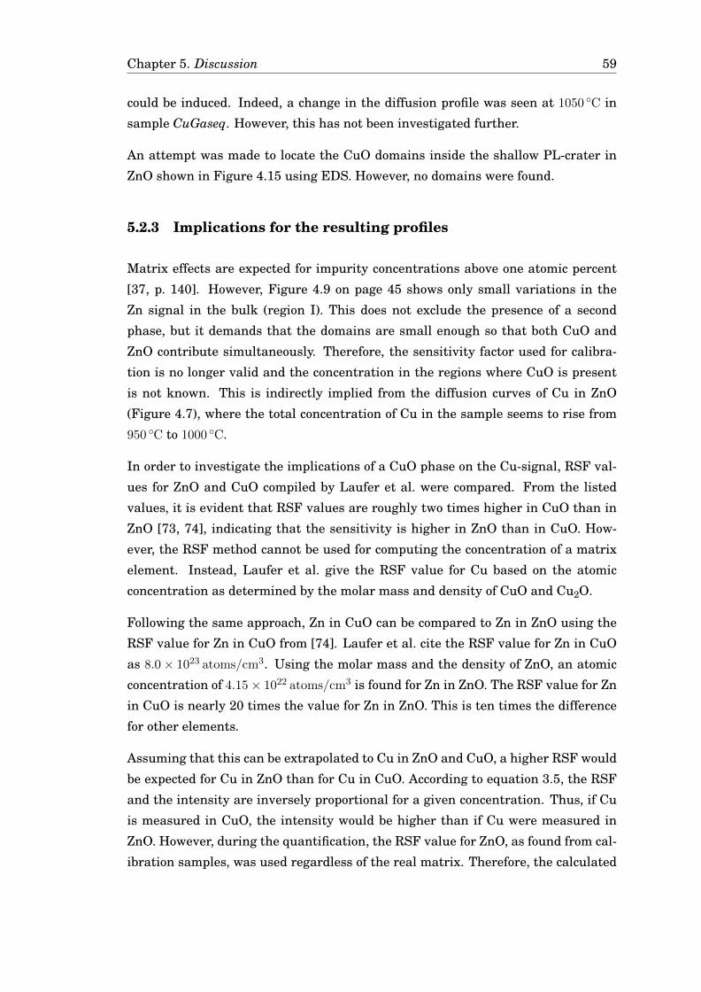
Chapter 5. Discussion 59
could be induced. Indeed, a change in the diffusion profile was seen at 1050 C in
sample CuGaseq. However, this has not been investigated further.
An attempt was made to locate the CuO domains inside the shallow PL-crater in
ZnO shown in Figure 4.15 using EDS. However, no domains were found.
5.2.3 Implications for the resulting profiles
Matrix effects are expected for impurity concentrations above one atomic percent
[37, p. 140]. However, Figure 4.9 on page 45 shows only small variations in the
Zn signal in the bulk (region I). This does not exclude the presence of a second
phase, but it demands that the domains are small enough so that both CuO and
ZnO contribute simultaneously. Therefore, the sensitivity factor used for calibra-
tion is no longer valid and the concentration in the regions where CuO is present
is not known. This is indirectly implied from the diffusion curves of Cu in ZnO
(Figure 4.7), where the total concentration of Cu in the sample seems to rise from
950 C to 1000 C.
In order to investigate the implications of a CuO phase on the Cu-signal, RSF val-
ues for ZnO and CuO compiled by Laufer et al. were compared. From the listed
values, it is evident that RSF values are roughly two times higher in CuO than in
ZnO [73, 74], indicating that the sensitivity is higher in ZnO than in CuO. How-
ever, the RSF method cannot be used for computing the concentration of a matrix
element. Instead, Laufer et al. give the RSF value for Cu based on the atomic
concentration as determined by the molar mass and density of CuO and Cu2O.
Following the same approach, Zn in CuO can be compared to Zn in ZnO using the
RSF value for Zn in CuO from [74]. Laufer et al. cite the RSF value for Zn in CuO
as 8.0× 10²³ atoms/cm3. Using the molar mass and the density of ZnO, an atomic
concentration of 4.15× 10²² atoms/cm3 is found for Zn in ZnO. The RSF value for Zn
in CuO is nearly 20 times the value for Zn in ZnO. This is ten times the difference
for other elements.
Assuming that this can be extrapolated to Cu in ZnO and CuO, a higher RSF would
be expected for Cu in ZnO than for Cu in CuO. According to equation 3.5, the RSF
and the intensity are inversely proportional for a given concentration. Thus, if Cu
is measured in CuO, the intensity would be higher than if Cu were measured in
ZnO. However, during the quantification, the RSF value for ZnO, as found from cal-
ibration samples, was used regardless of the real matrix. Therefore, the calculated
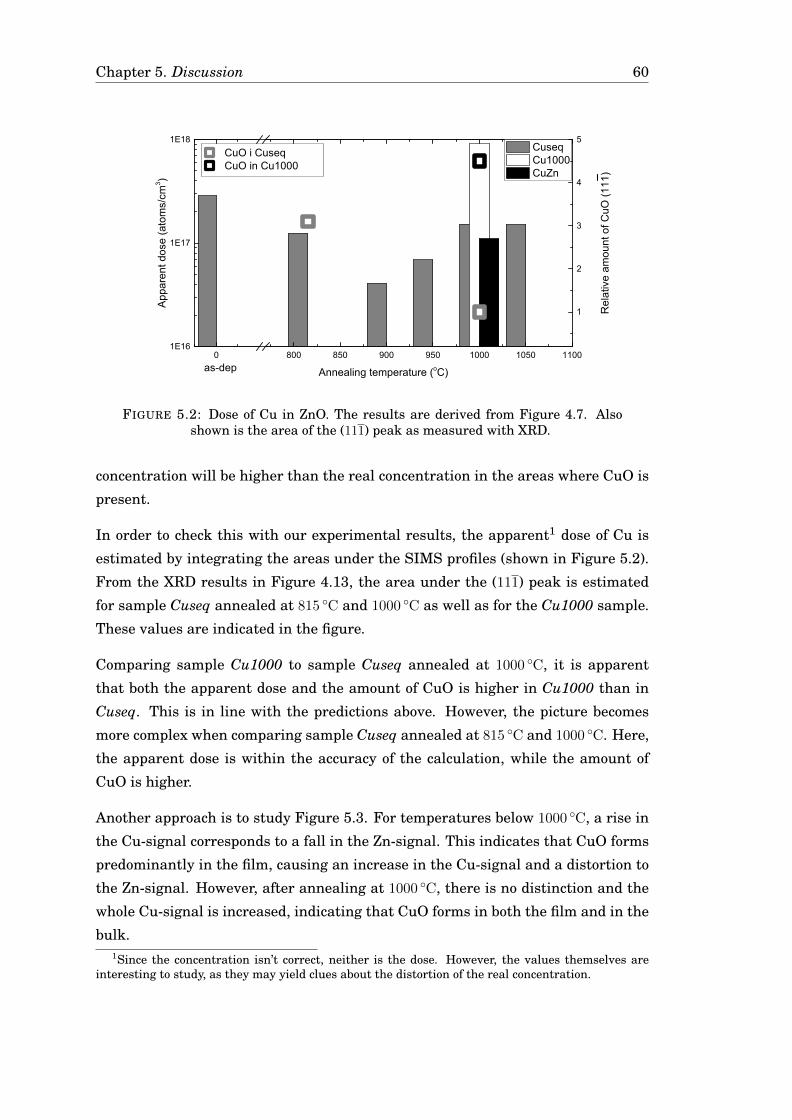
Chapter 5. Discussion 60
0 800 850 900 950 1000 1050 11001E16
1E17
1E18 Cuseq Cu1000 CuZn
App
aren
t dos
e (a
tom
s/cm
3 )
Annealing temperature (oC)as-dep
1
2
3
4
5 CuO i Cuseq CuO in Cu1000
Rel
ativ
e am
ount
of C
uO (1
11)
FIGURE 5.2: Dose of Cu in ZnO. The results are derived from Figure 4.7. Alsoshown is the area of the (111) peak as measured with XRD.
concentration will be higher than the real concentration in the areas where CuO is
present.
In order to check this with our experimental results, the apparent1 dose of Cu is
estimated by integrating the areas under the SIMS profiles (shown in Figure 5.2).
From the XRD results in Figure 4.13, the area under the (111) peak is estimated
for sample Cuseq annealed at 815 C and 1000 C as well as for the Cu1000 sample.
These values are indicated in the figure.
Comparing sample Cu1000 to sample Cuseq annealed at 1000 C, it is apparent
that both the apparent dose and the amount of CuO is higher in Cu1000 than in
Cuseq. This is in line with the predictions above. However, the picture becomes
more complex when comparing sample Cuseq annealed at 815 C and 1000 C. Here,
the apparent dose is within the accuracy of the calculation, while the amount of
CuO is higher.
Another approach is to study Figure 5.3. For temperatures below 1000 C, a rise in
the Cu-signal corresponds to a fall in the Zn-signal. This indicates that CuO forms
predominantly in the film, causing an increase in the Cu-signal and a distortion to
the Zn-signal. However, after annealing at 1000 C, there is no distinction and the
whole Cu-signal is increased, indicating that CuO forms in both the film and in the
bulk.1Since the concentration isn’t correct, neither is the dose. However, the values themselves are
interesting to study, as they may yield clues about the distortion of the real concentration.
Chapter 5. Discussion 61
0 2 4 6 8
1E17
1E18
1E19
1E20
1E21
as-dep 815 oC 900 oC 950 oC 1000 oC 1050 oC
63C
u co
ncen
tratio
n (a
tom
s/cm
3 )
1000
10000
Depth (um)
Inte
nsity
of 70
Zn-s
igna
l (co
unts
/s)
63Cu
70Zn
FIGURE 5.3: Cu-signal and Zn-signal versus depth for sample Cuseq.
5.3 A scenario for the diffusion of Ag/Cu in ZnO
Based on the results in the previous section, only diffusion profiles in region III of
ZnO and below 1× 10¹⁹ atoms/cm3 for GZO are considered for Cu.
Both Cu and Ag show a strong Fermi level position dependence, where the diffusion
is enhanced when annealed in the heavily doped GZO substrate. If the formation
energy of possible charged defects is considered, it is clear that the formation energy
of interstitial Ag must increase as the Fermi level increases, while the opposite is
true for substitutional Ag. Since diffusion is enhanced in GZO, which has a higher
Fermi level position than ZnO due to the Ga-doping, the diffusion in GZO is more
likely to be caused by substitutional Ag, since both their formation energies, as
well as the formation energy of Zn-vacancies, are lower in GZO, as compared to
ZnO. The same argument can be made for Cu.
The indication of substitutional impurities points to a vacancy-mediated diffusion
process2. This is further supported by the fact that (i) the diffusion can be sup-
pressed by annealing in a Zn-rich atmosphere and (ii) that substitutional Cu was
indicated by PL. Although a vacancy-mediated diffusion process seems likely for2The vacancy-mediated diffusion referred to here and in the subsequent paragraphs is the diffu-
sion by vZn.
Chapter 5. Discussion 62
both elements, the corresponding diffusion coefficients are expected to be different
since the diffusion processes start at different temperatures, have different solubil-
ities and different shapes.
Despite the clear indications of a vacancy-mediated diffusion, it cannot alone ex-
plain the results. In particular, the results for the samples annealed in a Zn-rich
atmosphere, i.e., the pile-up seen in sample CuZn and the low-concentration profile
in sample AgGaZn, cannot be explained by a vacancy-mediated diffusion. These
results point to a rapid diffusion with a low solubility, and interstitial diffusion is
a candidate for these features. In addition, the PL-measurements may indirectly
indicate an interstitial component. For the middle crater in sample Cu1000, the
near-band emission is lower than for the deep crater in the same sample. If nor-
malized, however, the deep band emission of the middle crater rises above that of
the deep crater so that the difference in intensity is 3-4 times larger than the dif-
ference in concentration. This could indicate that some Cu exist as Cui in region
III.
An interstitial diffusion component would be enhanced when the annealing is done
in a Zn-rich atmosphere and at low Fermi level positions, and suppressed when the
annealing is done in an oxygen-rich environment and at high Fermi level positions
[75, p. 16]. In ZnO, both the vacancy-mediated and the interstitial diffusion could
be present, explaining the very deep diffusion profile found in undoped ZnO.
5.4 Computational results for vacancy-mediated diffu-sion models
A vacancy-mediated diffusion will be modelled for both Ag and Cu. The model
as well as its discrepancies with the experimental data will then be put into the
context of the scenario explained above. For the diffusion of Ag at low temperatures,
there are no experimental profiles to model. Similarly, for the diffusion profiles of
Cu in ZnO, there is very little dynamics left to model. For the diffusions in GZO,
however, the results can be modelled.
5.4.1 A model for the diffusion of Ag in GZO
The diffusion of Ag in GZO can be modelled using Fick’s second law, as explained
in Section 2.2.1, to determine the diffusion coefficient at each temperature. Rather
than using the complementary error function solution as shown in equation 2.17
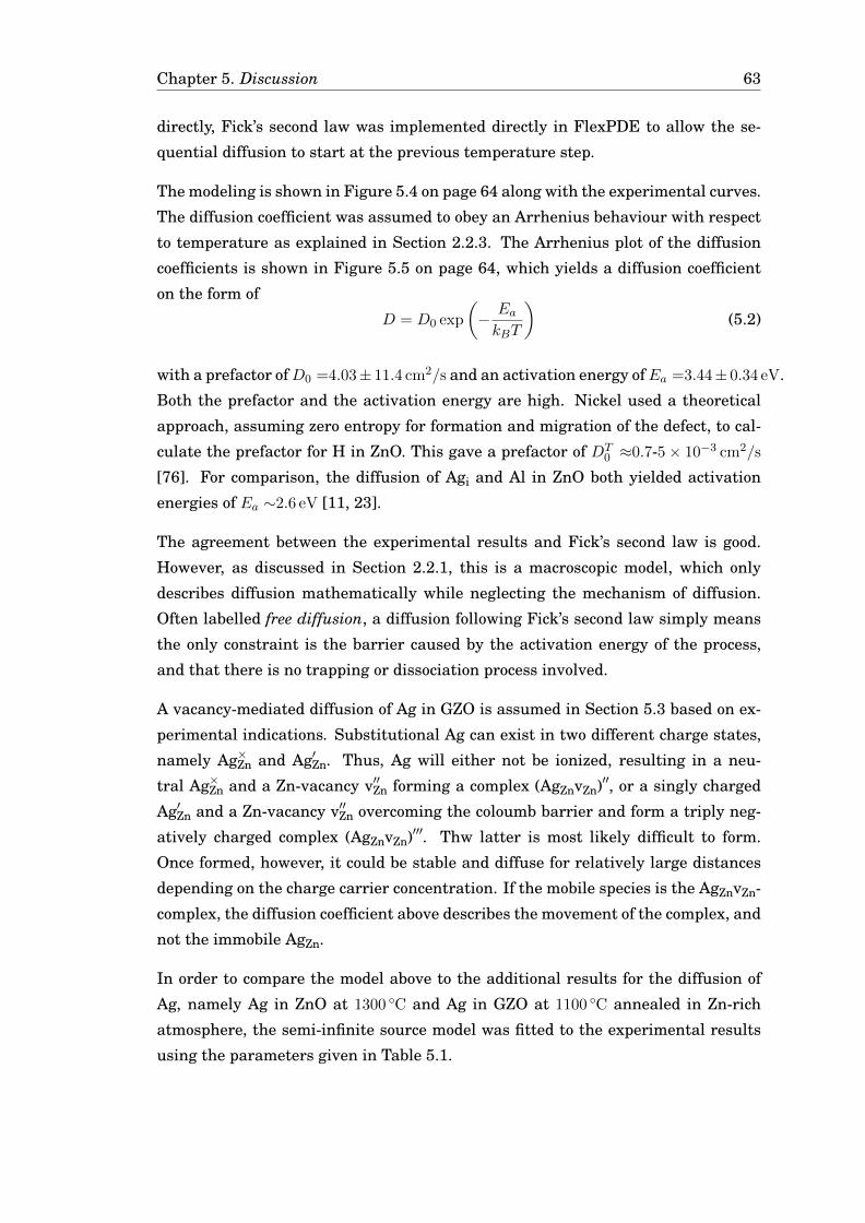
Chapter 5. Discussion 63
directly, Fick’s second law was implemented directly in FlexPDE to allow the se-
quential diffusion to start at the previous temperature step.
The modeling is shown in Figure 5.4 on page 64 along with the experimental curves.
The diffusion coefficient was assumed to obey an Arrhenius behaviour with respect
to temperature as explained in Section 2.2.3. The Arrhenius plot of the diffusion
coefficients is shown in Figure 5.5 on page 64, which yields a diffusion coefficient
on the form of
D = D0 exp
(− EakBT
)(5.2)
with a prefactor ofD0 =4.03± 11.4 cm2/s and an activation energy ofEa =3.44± 0.34 eV.
Both the prefactor and the activation energy are high. Nickel used a theoretical
approach, assuming zero entropy for formation and migration of the defect, to cal-
culate the prefactor for H in ZnO. This gave a prefactor of DT0 ≈0.7-5× 10⁻³ cm2/s
[76]. For comparison, the diffusion of Agi and Al in ZnO both yielded activation
energies of Ea ∼2.6 eV [11, 23].
The agreement between the experimental results and Fick’s second law is good.
However, as discussed in Section 2.2.1, this is a macroscopic model, which only
describes diffusion mathematically while neglecting the mechanism of diffusion.
Often labelled free diffusion, a diffusion following Fick’s second law simply means
the only constraint is the barrier caused by the activation energy of the process,
and that there is no trapping or dissociation process involved.
A vacancy-mediated diffusion of Ag in GZO is assumed in Section 5.3 based on ex-
perimental indications. Substitutional Ag can exist in two different charge states,
namely Ag×Zn and Ag′Zn. Thus, Ag will either not be ionized, resulting in a neu-
tral Ag×Zn and a Zn-vacancy v′′Zn forming a complex (AgZnvZn)′′, or a singly charged
Ag′Zn and a Zn-vacancy v′′Zn overcoming the coloumb barrier and form a triply neg-
atively charged complex (AgZnvZn)′′′. Thw latter is most likely difficult to form.
Once formed, however, it could be stable and diffuse for relatively large distances
depending on the charge carrier concentration. If the mobile species is the AgZnvZn-
complex, the diffusion coefficient above describes the movement of the complex, and
not the immobile AgZn.
In order to compare the model above to the additional results for the diffusion of
Ag, namely Ag in ZnO at 1300 C and Ag in GZO at 1100 C annealed in Zn-rich
atmosphere, the semi-infinite source model was fitted to the experimental results
using the parameters given in Table 5.1.
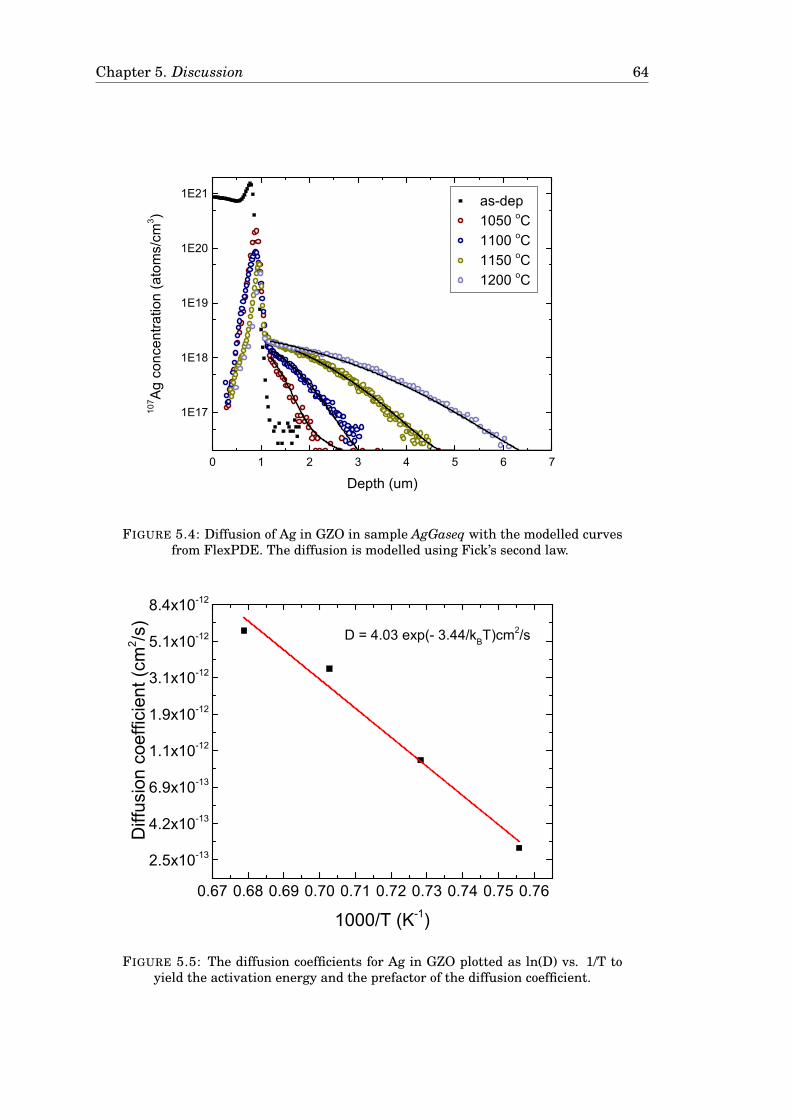
Chapter 5. Discussion 64
0 1 2 3 4 5 6 7
1E17
1E18
1E19
1E20
1E21
Depth (um)
as-dep 1050 oC 1100 oC 1150 oC 1200 oC
107 A
g co
ncen
tratio
n (a
tom
s/cm
3 )
FIGURE 5.4: Diffusion of Ag in GZO in sample AgGaseq with the modelled curvesfrom FlexPDE. The diffusion is modelled using Fick’s second law.
0.67 0.68 0.69 0.70 0.71 0.72 0.73 0.74 0.75 0.76
2.5x10⁻¹³
4.2x10⁻¹³
6.9x10⁻¹³
1.1x10⁻¹²
1.9x10⁻¹²
3.1x10⁻¹²
5.1x10⁻¹²
8.4x10⁻¹²
Diff
usio
n co
effic
ient
(cm
2 /s)
1000/T (K-1)
D = 4.03 exp(- 3.44/kBT)cm2/s
FIGURE 5.5: The diffusion coefficients for Ag in GZO plotted as ln(D) vs. 1/T toyield the activation energy and the prefactor of the diffusion coefficient.
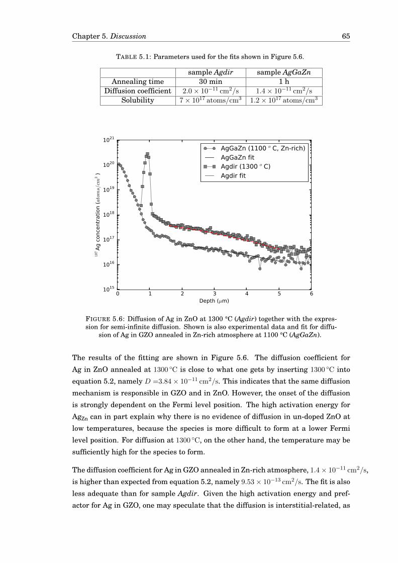
Chapter 5. Discussion 65
TABLE 5.1: Parameters used for the fits shown in Figure 5.6.
sample Agdir sample AgGaZnAnnealing time 30 min 1 h
Diffusion coefficient 2.0× 10⁻¹¹ cm2/s 1.4× 10⁻¹¹ cm2/s
Solubility 7× 10¹⁷ atoms/cm3 1.2× 10¹⁷ atoms/cm3
0 1 2 3 4 5 6Depth (µm)
1015
1016
1017
1018
1019
1020
1021
107
Ag c
once
ntration (atoms/cm
3)
AgGaZn (1100 o C, Zn-rich)
AgGaZn fitAgdir (1300 o C)
Agdir fit
FIGURE 5.6: Diffusion of Ag in ZnO at 1300 °C (Agdir) together with the expres-sion for semi-infinite diffusion. Shown is also experimental data and fit for diffu-
sion of Ag in GZO annealed in Zn-rich atmosphere at 1100 °C (AgGaZn).
The results of the fitting are shown in Figure 5.6. The diffusion coefficient for
Ag in ZnO annealed at 1300 C is close to what one gets by inserting 1300 C into
equation 5.2, namely D =3.84× 10⁻¹¹ cm2/s. This indicates that the same diffusion
mechanism is responsible in GZO and in ZnO. However, the onset of the diffusion
is strongly dependent on the Fermi level position. The high activation energy for
AgZn can in part explain why there is no evidence of diffusion in un-doped ZnO at
low temperatures, because the species is more difficult to form at a lower Fermi
level position. For diffusion at 1300 C, on the other hand, the temperature may be
sufficiently high for the species to form.
The diffusion coefficient for Ag in GZO annealed in Zn-rich atmosphere, 1.4× 10⁻¹¹ cm2/s,
is higher than expected from equation 5.2, namely 9.53× 10⁻¹³ cm2/s. The fit is also
less adequate than for sample Agdir. Given the high activation energy and pref-
actor for Ag in GZO, one may speculate that the diffusion is interstitial-related, as
Chapter 5. Discussion 66
the diffusivity is higher and the solubility lower.
5.4.2 Cu in GZO modelled with the Reaction-diffusion model
For Cu in GZO, a fruitless attempt was made to fit the semi-infinite source model to
the data. As a vacancy-mediated mechanism was still suspected, the more complex
reaction-diffusion model developed by Johansen et al. for the diffusion of Al in ZnO
[11] was used to model the diffusion.
Reaction-diffusion can be modelled by describing the behaviour of a substitutional
defect, a vacancy and the vacancy–substitutional defect complex. The defects vZn,
(CuZnvZn) and CuZn will therefore be included, as well as the electron concentration,
n. The behaviour of CuZn and (CuZnvZn) is described by defect reactions. The con-
centration of Zn-vacancies, however, is described by using their formation energy.
This is done by acknowledging that the time scale for formation and distribution
of vacancies is much smaller than the time scale for the other processes involved.
Thus, the formation and distribution of vacancies can be seen as happening in-
stantaneously. The use of formation energies also allows for easy inclusion of the
different charge states of the defects. According to DFT predictions for vZn [11], the
Zn-vacancy can be both singly or doubly charged for the Fermi level positions of
interest. Both these states are included in the model. CuZn can be both neutral or
negatively charged [18]. It will be assumed that only the complex with charge -2
can be formed. Therefore, the charge of CuZn will only matter in the expression for
n.
This gives us the following set of equations:
[v′′Zn] = A(v′′Zn)n2 (5.3)
[v′Zn] = A(v′Zn)n (5.4)
d
dt[CuZnv′′Zn] = D
d2
dx2[CuZnv′′Zn]− d
dt[Cutot
Zn] (5.5)
d
dt[Cutot
Zn] = [CuZnvZn]ν −([v′′Zn] + [v′Zn]
)[Cutot
Zn]K (5.6)
d
dtn =
d
dt
(nd − 2[v′′Zn]− [v′Zn]− 2[CuZnv′′Zn]− [Cutot
Zn]
(1
1 + Bn
))(5.7)
K is a trapping coefficient K = 4πRDvZn , where DvZn is the diffusion coefficient for
the Zn-vacancy and R is a trap capture radius. R is kept constant at R = 1 nm,
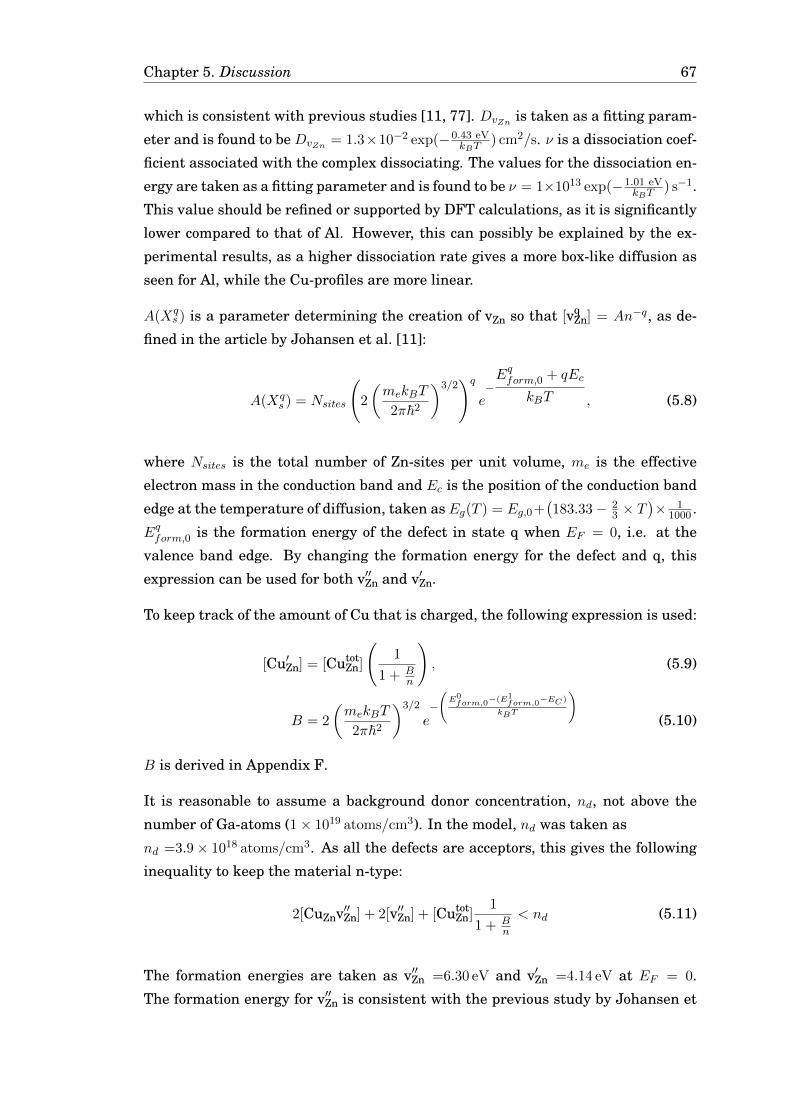
Chapter 5. Discussion 67
which is consistent with previous studies [11, 77]. DvZn is taken as a fitting param-
eter and is found to be DvZn = 1.3×10⁻² exp(−0.43 eVkBT
) cm2/s. ν is a dissociation coef-
ficient associated with the complex dissociating. The values for the dissociation en-
ergy are taken as a fitting parameter and is found to be ν = 1×10¹³ exp(−1.01 eVkBT
) s−1.
This value should be refined or supported by DFT calculations, as it is significantly
lower compared to that of Al. However, this can possibly be explained by the ex-
perimental results, as a higher dissociation rate gives a more box-like diffusion as
seen for Al, while the Cu-profiles are more linear.
A(Xqs ) is a parameter determining the creation of vZn so that [vq
Zn] = An−q, as de-
fined in the article by Johansen et al. [11]:
A(Xqs ) = Nsites
(2
(mekBT
2π~2
)3/2)q
e−Eqform,0 + qEc
kBT , (5.8)
where Nsites is the total number of Zn-sites per unit volume, me is the effective
electron mass in the conduction band and Ec is the position of the conduction band
edge at the temperature of diffusion, taken as Eg(T ) = Eg,0+(183.33− 2
3 × T)× 1
1000 .
Eqform,0 is the formation energy of the defect in state q when EF = 0, i.e. at the
valence band edge. By changing the formation energy for the defect and q, this
expression can be used for both v′′Zn and v′Zn.
To keep track of the amount of Cu that is charged, the following expression is used:
[Cu′Zn] = [CutotZn]
(1
1 + Bn
), (5.9)
B = 2
(mekBT
2π~2
)3/2
e−(
E0form,0−(E1
form,0−EC )
kBT
)(5.10)
B is derived in Appendix F.
It is reasonable to assume a background donor concentration, nd, not above the
number of Ga-atoms (1× 10¹⁹ atoms/cm3). In the model, nd was taken as
nd =3.9× 10¹⁸ atoms/cm3. As all the defects are acceptors, this gives the following
inequality to keep the material n-type:
2[CuZnv′′Zn] + 2[v′′Zn] + [CutotZn]
1
1 + Bn
< nd (5.11)
The formation energies are taken as v′′Zn =6.30 eV and v′Zn =4.14 eV at EF = 0.
The formation energy for v′′Zn is consistent with the previous study by Johansen et
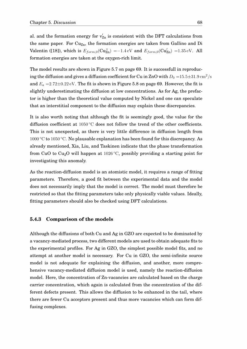
Chapter 5. Discussion 68
al. and the formation energy for v′Zn is consistent with the DFT calculations from
the same paper. For CuZn, the formation energies are taken from Gallino and Di
Valentin ([18]), which is Eform,0(Cu×Zn) =−1.4 eV and Eform,0(Cu′Zn) =1.35 eV. All
formation energies are taken at the oxygen-rich limit.
The model results are shown in Figure 5.7 on page 69. It is successfull in reproduc-
ing the diffusion and gives a diffusion coefficient for Cu in ZnO withD0 =15.5±31.9 cm2/s
and Ea =2.72±0.22 eV. The fit is shown in Figure 5.8 on page 69. However, the fit is
slightly underestimating the diffusion at low concentrations. As for Ag, the prefac-
tor is higher than the theoretical value computed by Nickel and one can speculate
that an interstitial component to the diffusion may explain these discrepancies.
It is also worth noting that although the fit is seemingly good, the value for the
diffusion coefficient at 1050 C does not follow the trend of the other coefficients.
This is not unexpected, as there is very little difference in diffusion length from
1000 C to 1050 C. No plausable explanation has been found for this discrepancy. As
already mentioned, Xia, Liu, and Taskinen indicate that the phase transformation
from CuO to Cu2O will happen at 1026 C, possibly providing a starting point for
investigating this anomaly.
As the reaction-diffusion model is an atomistic model, it requires a range of fitting
parameters. Therefore, a good fit between the experimental data and the model
does not necessarily imply that the model is correct. The model must therefore be
restricted so that the fitting parameters take only physically viable values. Ideally,
fitting parameters should also be checked using DFT calculations.
5.4.3 Comparison of the models
Although the diffusions of both Cu and Ag in GZO are expected to be dominated by
a vacancy-mediated process, two different models are used to obtain adequate fits to
the experimental profiles. For Ag in GZO, the simplest possible model fits, and no
attempt at another model is necessary. For Cu in GZO, the semi-infinite source
model is not adequate for explaining the diffusion, and another, more compre-
hensive vacancy-mediated diffusion model is used, namely the reaction-diffusion
model. Here, the concentration of Zn-vacancies are calculated based on the charge
carrier concentration, which again is calculated from the concentration of the dif-
ferent defects present. This allows the diffusion to be enhanced in the tail, where
there are fewer Cu acceptors present and thus more vacancies which can form dif-
fusing complexes.
Chapter 5. Discussion 69
0 2 4 6 8 10 12 14 161E16
1E17
1E18
1E19
1E20
63C
u co
ncen
tratio
n (a
tom
s/cm
3 )
Depth (um)
as-dep 850 oC 900 oC 950 oC 1000 oC 1050 oC 1100 oC
FIGURE 5.7: Diffusion of Cu in GZO in sample CuGaseq with the modelled curvesfrom FlexPDE. The diffusion is modelled using the vacancy model described above.
0.72 0.74 0.76 0.78 0.80 0.82 0.84 0.86 0.88 0.90
5.1x10⁻¹²
1.4x10⁻¹¹
3.8x10⁻¹¹
1.0x10⁻¹⁰
2.8x10⁻¹⁰
7.6x10⁻¹⁰
2.1x10⁻⁹
D = 15.5 exp(- 2.72/kBT)cm2/s
Diff
usio
n co
effic
ient
(cm
2 /s)
1000/T (K-1)
FIGURE 5.8: Diffusion coefficients for the reaction-diffusion model of Cu in GZO.The diffusion coefficient for 1050 C is excluded from the fit and the data point is
therefore red.
Chapter 5. Discussion 70
Both the free diffusion model for Ag and the reaction-diffusion model for Cu yield
higher values for the activation energy and prefactor than expected from theoretical
predictions by Nickel [76], who assumed zero entropy for formation and migration.
First principle-calculations have shown that adding entropy an entropy of 3 kB en-
hance the prefactor with a factor 20 [78]. However, an entropy effect cannot explain
that both the prefactor and the activation energy were higher than expected. One
possibility is that there is an interstitial component in both diffusion processes, in-
creasing both the activation energy and the prefactor. This is supported by studies
in Zn-rich atmosphere. Another possibility is that the low dissociation rate for Cu
in GZO allows the complex to diffuse deeper, resulting in a high prefactor, and that
the high activation energies for both Ag and Cu reflect the Coulomb repulsion in
forming the complex.
5.5 Comparison to other diffusion experiments
Diffusion of Ag in ZnO was previously studied by Azarov et al. [23]. The studies
differ in the method of introducing the dopant. Azarov et al. introduced Ag by ion
implantation (see Figure 2.8 on page 22). This method allowed for a precise dose,
but inevitably created intrinsic defects when incoming ions created Frenkel defects,
i.e., self-interstitials and vacancies. In this case, particularly Agi and vZn created
by implantation are of interest because they can both contribute to the diffusion,
either directly or indirectly. The study indicated that interstitial (Agi) migration
prevailed and repored an activation energy of ∼2.6 eV for the trap-limited diffusion
of Agi. This is 0.8 eV lower than what was found above.
The methodology used in this work allowed for a less damaging introduction of
the dopant, which created fewer intrinsic defects. However, the diffusion was sup-
pressed, leading to the conclusion that the most mobile configuration of the im-
planted Ag ions, i.e., Agi is responsible for the diffusion observed by Azarov et al.
[23]. Furthermore, it is noticeable that the solubility, the diffusion length and the
form of the diffusion profile in GZO differ from those obtained by Azarov et al. [23],
supporting the claim that two different diffusion mechanisms are active.
The study by Azarov et al. showed a pile-up of Ag similar to that of Cu in ZnO an-
nealed in a Zn-rich atmosphere. The pile-up of Ag was attributed to local implantation-
induced stoichiometry disturbances which caused trapping of Ag atoms by O and
Zn vacancies [23]. The pile-up of Cu in ZnO cannot be explained by implanta-
tion–induced disturbances. Instead, the pile-up is believed to be caused by a rapid
Chapter 5. Discussion 71
interstitial diffusion at a low concentration where the diffusing species is trapped,
building up a detectable concentration.
Al was studied by Johansen et al. [11], where the reaction-diffusion model was de-
veloped. This model was adapted to Cu with some success. The difference between
Cu and Al in profile shape was accounted for by a lower dissociation rate in the
former case, which caused the complex to diffuse deeper, going from the box-like
diffusion of Al to the almost linear diffusion of Cu. The activation energy for Cu in
GZO was found to be 2.72 eV which is comparable to 2.6 eV, the activation energy
for Al in ZnO [11]. However, the diffusion length is much longer for Cu than for
Al, possibly supporting the suggestion that a secondary, rapid interstitial process
at operation is causing an activation energy higher than would be expected for the
vacancy-mediated diffusion alone.
Similar diffusion experiments for Ni in ZnO were performed by Sky [48]. The study
suggested that both a vacancy mediated and an interstitial mechanism were re-
sponsible for the diffusion of Ni in ZnO. This is in line with the results presented
for Ag and Cu.

Chapter 6
Summary
The diffusion mechanisms of Ag and Cu in monocrystalline ZnO have been in-
vestigated by sequentially annealing and probing ZnO substrates doped by in-
diffusion from Cu-doped and Ag-doped ZnO films. The diffusion has been ma-
nipulated through changing the Fermi level positions and the stoichiometries of
the samples. Complementary measurements have been provided using XRD, EDS,
SSRM and PL.
6.1 Conclusion
Both Ag and Cu belong to group 11 in the periodic table, and both elements have
one electron in the valence shell, which makes them possible candidates for p-type
doping. Ag had been previously studied in a similar experiment by Azarov et al.
[23], while Cu had been studied by Herklotz, Lavrov, and Weber by using FTIR
[49]. The two elements were therefore considered as a good starting point for a
diffusion study of potential p-type dopants.
Both Ag and Cu are assumed to diffuse by a combination of vacancy–mediated dif-
fusion and interstitial diffusion. Vacancy-mediated diffusion dominates when the
Fermi level position was high, while interstitial diffusion dominates when the sam-
ples were annealed in a Zn-rich atmosphere, suppressing the Zn-vacancies. The
interstitial diffusion exhibits a lower solubility than the vacancy-mediated diffu-
sion.
The Ag diffusion fits the semi-infinite diffusion model with a diffusion coefficient of
D =4.03exp(−3.44 eVkBT
) cm2/s for Ag in GZO. The high activation energy of the process
73
Chapter 6. Summary 74
inhibits diffusion in ZnO, but can be overcome by raising the temperature signif-
icantly or by altering the Fermi level. Although the activation energy is expected
to be relatively high, both the activation energy and the prefactor are likely to be
affected by the interstitial diffusion process, causing both a higher prefactor and a
higher activation energy than expected.
The diffusion of Cu in ZnO is attributed to the reaction-diffusion model, as de-
scribed in [11]. This model yields a diffusion coefficient ofD =15.5exp(−2.72 eVkBT
) cm2/s
for the CuZnvZn-complex diffusing in GZO. Enhancement of the diffusion is observed
when the Fermi level is raised, supporting the hypothesis of a vacancy-mediated
diffusion process. Through annealing, CuO domains are formed in the sample.
These domains are present in both the film and the bulk, altering the matrix of the
ZnO and increasing the Cu-signal.
Both Ag and Cu can act as acceptors in ZnO, and this was the original reason
for studying these two elements. However, the diffusion in undoped substrates is
restricted to low concentrations. Their ability to diffuse at great lengths as acceptor
type species in the heavily doped n-type substrate is, although interesting, less
relevant to the p-type perspective as dopants. When the material is less n-type,
the solubility of the dopants is low. However, the diffusion at low concentrations is
enhanced when annealed in a Zn-rich atmosphere, which supresses the formation
of Zn-vacancies.
6.2 Suggestions for further work
As this study was qualitative and exploratory in nature, it returned many ideas for
further research.
The theoretical foundation for diffusion of Cu in ZnO is scarce, and density func-
tional theory (DFT) should be employed to investigate the formation energies of
Cui and CuZn to confirm the validity of the model proposed in this thesis. As DFT
calculations vary widely according to the method used, the calculations should also
be done for Ag to ensure comparable results.
The diffusion of both Ag and Cu showed a strong Fermi level position dependence.
This could be studied further by aquiring more samples with different background
doping levels, making it possible to do series of measurements to determine the
effect of the doping more closely. As the vacancy-mediated diffusion was enhanced
when the Fermi level position was high, this could also be used to distinguish be-
tween the vacancy-mediated diffusion and the interstitial diffusion. To isolate the
Chapter 6. Summary 75
interstitial diffusion, an isochronal series could be performed in a Zn-rich atmo-
sphere. It was noticed that the diffusion of Ag and Cu started at different tem-
peratures. However, no isothermal studies were performed. This could be used to
distinguish between the insterstitial and vacancy processes and further investigate
the solubility of the two elements.
The anomaly in Cu-doped GZO at 1050 C, where there is suddenly very little dif-
fusion, has been mentioned several times. No theory exists for this behaviour, but
it was mentioned that it coincides with the transformation from CuO to Cu2O at
1026 C. Isothermal studies of Cu in ZnO could be performed at both 1000 C and
1050 C to investigate the origin of this behaviour.
The presence and distribution of CuO in the ZnO should be investigated further. If
separate domains are present, these could be seen by Transmission Electron Mi-
croscopy (TEM) or investigated by Cathode luminescence (CL) spectroscopy. TEM
could also indicate whether the CuO forms locally or as three-dimensional finger-
like strucures. Another possibility would be to polish down the film of the existing
samples to allow investigation by XPS.
Finally, this work is characteristic of an investigative first attempt to survey a vir-
gin field. Therefore, various samples have been investigated with different meth-
ods in order to support or falsify various ideas that emerged during the study. The
SIMS profiles are thus the only measurement done for all samples. However, this
has allowed for the testing of several hypothesis, but it does not give any conclu-
sive evidence. Hopefully, a more comprehensive study can be designed from these
results, tailored to investigate certain properties more thoroughly.

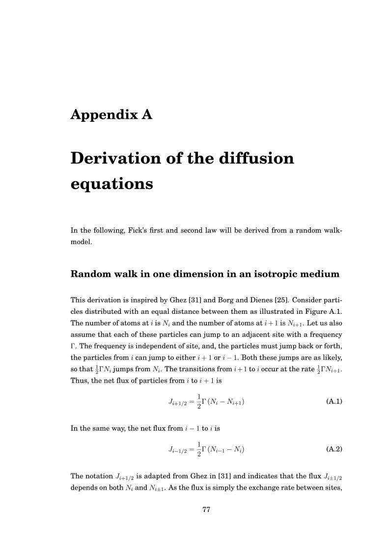
Appendix A
Derivation of the diffusionequations
In the following, Fick’s first and second law will be derived from a random walk-
model.
Random walk in one dimension in an isotropic medium
This derivation is inspired by Ghez [31] and Borg and Dienes [25]. Consider parti-
cles distributed with an equal distance between them as illustrated in Figure A.1.
The number of atoms at i is Ni and the number of atoms at i+ 1 is Ni+1. Let us also
assume that each of these particles can jump to an adjacent site with a frequency
Γ. The frequency is independent of site, and, the particles must jump back or forth,
the particles from i can jump to either i+ 1 or i− 1. Both these jumps are as likely,
so that 12ΓNi jumps from Ni. The transitions from i+1 to i occur at the rate 1
2ΓNi+1.
Thus, the net flux of particles from i to i+ 1 is
Ji+1/2 =1
2Γ (Ni −Ni+1) (A.1)
In the same way, the net flux from i− 1 to i is
Ji−1/2 =1
2Γ (Ni−1 −Ni) (A.2)
The notation Ji+1/2 is adapted from Ghez in [31] and indicates that the flux Ji±1/2depends on both Ni and Ni±1. As the flux is simply the exchange rate between sites,
77
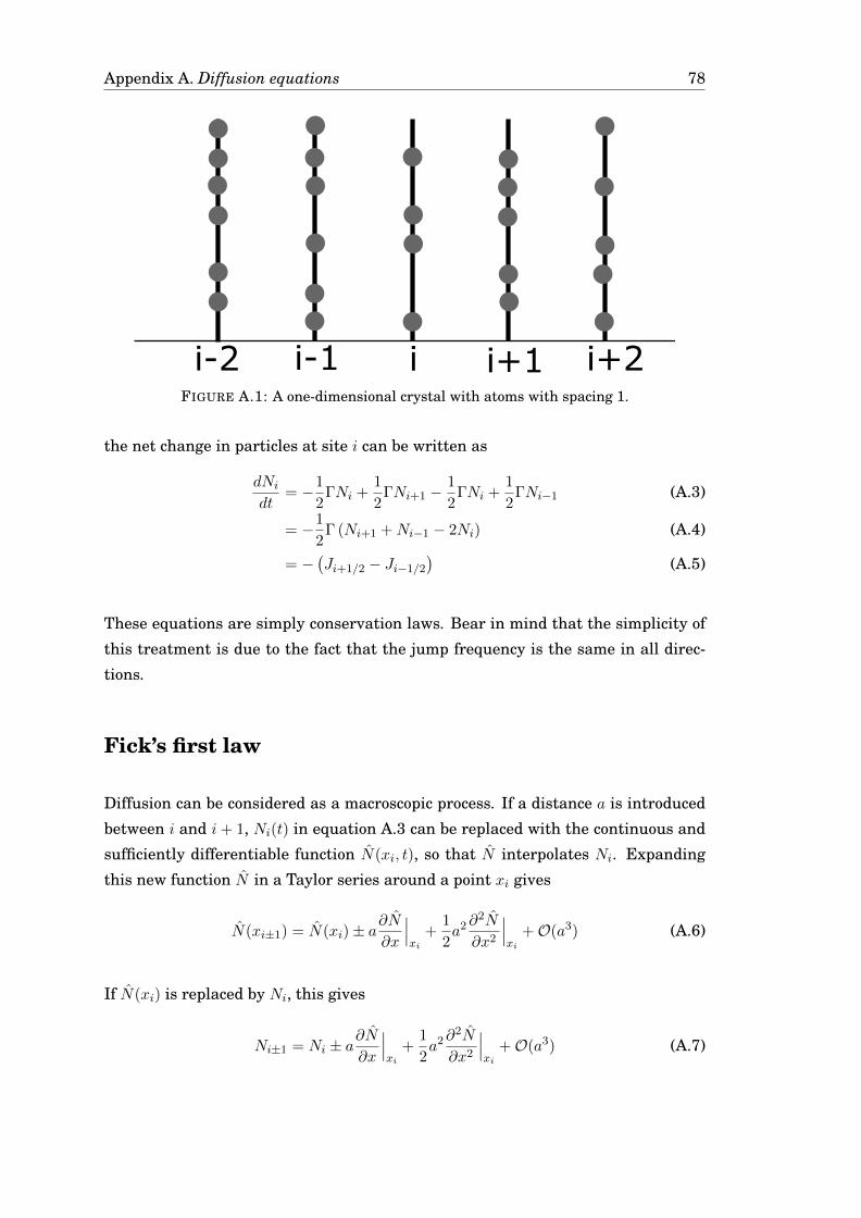
Appendix A. Diffusion equations 78
i i+1i-2 i-1 i+2FIGURE A.1: A one-dimensional crystal with atoms with spacing 1.
the net change in particles at site i can be written as
dNi
dt= −1
2ΓNi +
1
2ΓNi+1 −
1
2ΓNi +
1
2ΓNi−1 (A.3)
= −1
2Γ (Ni+1 +Ni−1 − 2Ni) (A.4)
= −(Ji+1/2 − Ji−1/2
)(A.5)
These equations are simply conservation laws. Bear in mind that the simplicity of
this treatment is due to the fact that the jump frequency is the same in all direc-
tions.
Fick’s first law
Diffusion can be considered as a macroscopic process. If a distance a is introduced
between i and i+ 1, Ni(t) in equation A.3 can be replaced with the continuous and
sufficiently differentiable function N(xi, t), so that N interpolates Ni. Expanding
this new function N in a Taylor series around a point xi gives
N(xi±1) = N(xi)± a∂N
∂x
∣∣∣xi
+1
2a2∂2N
∂x2
∣∣∣xi
+O(a3) (A.6)
If N(xi) is replaced by Ni, this gives
Ni±1 = Ni ± a∂N
∂x
∣∣∣xi
+1
2a2∂2N
∂x2
∣∣∣xi
+O(a3) (A.7)
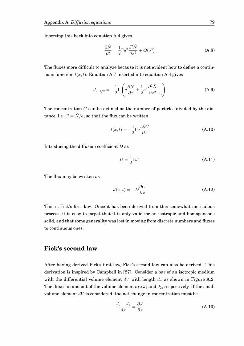
Appendix A. Diffusion equations 79
Inserting this back into equation A.4 gives
∂N
∂t=
1
2Γa2
∂2N
∂x2+O(a4) (A.8)
The fluxes more difficult to analyze because it is not evident how to define a contin-
uous function J(x, t). Equation A.7 inserted into equation A.4 gives
Ji±1/2 = −1
2Γ
(a∂N
∂x± 1
2a2∂2N
∂x2
∣∣∣xi
)(A.9)
The concentration C can be defined as the number of particles divided by the dis-
tance, i.e. C = N/a, so that the flux can be written
J(x, t) = −1
2Γaa∂C
∂x(A.10)
Introducing the diffusion coefficient D as
D =1
2Γa2 (A.11)
The flux may be written as
J(x, t) = −D∂C∂x
(A.12)
This is Fick’s first law. Once it has been derived from this somewhat meticulous
process, it is easy to forget that it is only valid for an isotropic and homogeneous
solid, and that some generality was lost in moving from discrete numbers and fluxes
to continuous ones.
Fick’s second law
After having derived Fick’s first law, Fick’s second law can also be derived. This
derivation is inspired by Campbell in [27]. Consider a bar of an isotropic medium
with the differential volume element dV with length dx as shown in Figure A.2.
The fluxes in and out of the volume element are J1 and J2, respectively. If the small
volume element dV is considered, the net change in concentration must be
J2 − J1dx
=∂J
∂x(A.13)
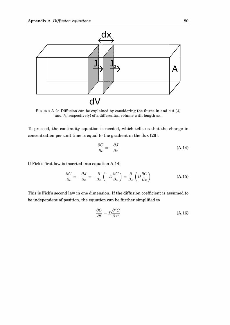
Appendix A. Diffusion equations 80
dx
dVFIGURE A.2: Diffusion can be explained by considering the fluxes in and out (J1
and J2, respectively) of a differential volume with length dx.
To proceed, the continuity equation is needed, which tells us that the change in
concentration per unit time is equal to the gradient in the flux [26]:
∂C
∂t= −∂J
∂x(A.14)
If Fick’s first law is inserted into equation A.14:
∂C
∂t= −∂J
∂x= − ∂
∂x
(−D∂C
∂x
)=
∂
∂x
(D∂C
∂x
)(A.15)
This is Fick’s second law in one dimension. If the diffusion coefficient is assumed to
be independent of position, the equation can be further simplified to
∂C
∂t= D
∂2C
∂x2(A.16)
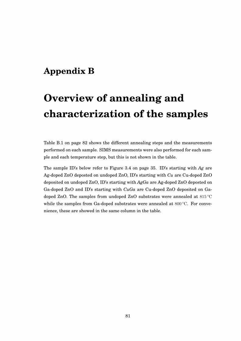
Appendix B
Overview of annealing andcharacterization of the samples
Table B.1 on page 82 shows the different annealing steps and the measurements
performed on each sample. SIMS measurements were also performed for each sam-
ple and each temperature step, but this is not shown in the table.
The sample ID’s below refer to Figure 3.4 on page 35. ID’s starting with Ag are
Ag-doped ZnO deposted on undoped ZnO, ID’s starting with Cu are Cu-doped ZnO
deposited on undoped ZnO, ID’s starting with AgGa are Ag-doped ZnO deposted on
Ga-doped ZnO and ID’s starting with CuGa are Cu-doped ZnO deposited on Ga-
doped ZnO. The samples from undoped ZnO substrates were annealed at 815 C
while the samples from Ga-doped substrates were annealed at 800 C. For conve-
nience, these are showed in the same column in the table.
81
Appendix
B.O
verviewofsam
ples82
TABLE B.1: Detailed table over the treatment and measurement of the different samples.
: XRD : PL : SSRM : Mass spectrum : EDS : Zn-rich atmosphere
ID as-dep 700 C 750 C 800/815 C 850 C 900 C 950 C 1000 C 1050 C 1100 C 1150 C 1200 C 1300 C
Ag1100 - - - - - - - - - ! - - -Agdir - - - - - - - ! - - - - !
Agseq - - - ! - ! ! ! ! - - - -
Agref - - - - - - - - - - - -
Cuseq - - - ! - ! ! ! ! - - - -
CuZn - - - - - - - ! - - - - -
Cu1000 - - - - - - - ! - - - - -
Curef - - - - - - - - - - - -AgGaseq - ! ! ! ! ! ! ! ! ! ! ! -
AgGaZn - - - - - - - - ! - - -
CuGaseq - ! ! ! ! ! ! ! ! ! - - -
CuGaref - - - - - - - - - - - -
Appendix C
Impurities in Ag:ZnO annealedat 1300 °C
At 1300 C, the introduction of impurities from the quartz tube is likely. Therefore,
a search for possible impurities was carried out, which is shown in Figure C.1 on
page 84. The intensities have not been calibrated, so the concentrations of the
different impurities are not known. However, the measurement give us an idea
about which impurities can be detected. Moreover, we can also study the shape of
the diffusion profiles for the different elements.
We notice that 27Al and 56Fe both have high intensities. According to Laufer et al.,
these elements have relatively high RSF values, from 1.0× 10²⁰ atoms/cm3 (Al) to
1.2× 10²¹ atoms/cm3 (Fe) , so these impurities are likely to be present in significant
amounts1. 23Na, on the other hand, has a lower intensity and a lower RSF, and
can be disregarded. We also notice a detectable amount of 55Mn og 60Ni. Both of
these have high RSF values (6.6× 10²⁰ atoms/cm3 for Mn and 4.3× 10²¹ atoms/cm3
for Ni), which indicates that they can be present in significant amounts, although
still an order of magnitude below Fe.
If we look at the shape of the profile of Fe, Mn and Ni, they bear close similarities.
This could be explained by mass interference effects, as discussed in Section 3.1.2,
which can lead us to detect 54Fe + 1H as 55Mn. This could fit the measured values,
as 54Fe should account for 5.845 % of the total amount of Fe [79]. From here, it
is easy to assume that Fe could also be responsible for the recorded 60Ni, which1The RSF values in the article are elemental RSF values, and they are thus not directly compara-
ble [73]. However, the uncertainties in the RSF values in the article are quoted to be 35%-50%, andthis will nevertheless account for a greater error than the mass lost in other isotopes for e.g. Fe
83
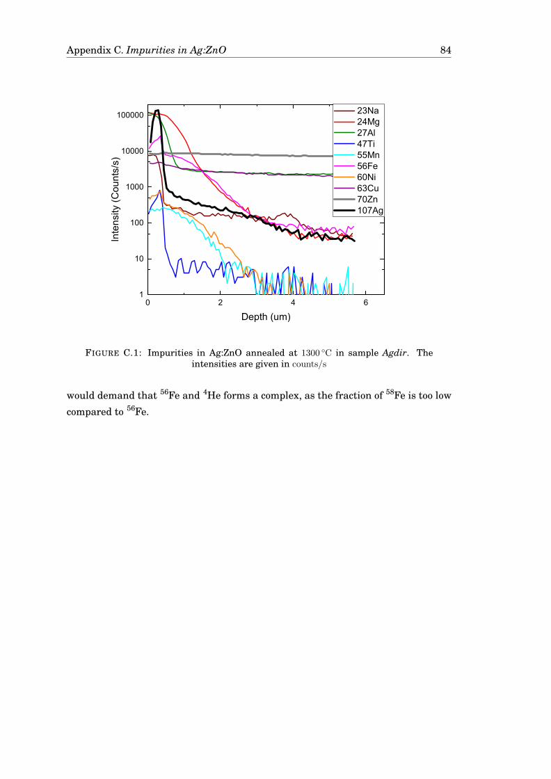
Appendix C. Impurities in Ag:ZnO 84
0 2 4 61
10
100
1000
10000
100000 23Na 24Mg 27Al 47Ti 55Mn 56Fe 60Ni 63Cu 70Zn 107Ag
Inte
nsity
(Cou
nts/
s)
Depth (um)
FIGURE C.1: Impurities in Ag:ZnO annealed at 1300 C in sample Agdir. Theintensities are given in counts/s
would demand that 56Fe and 4He forms a complex, as the fraction of 58Fe is too low
compared to 56Fe.
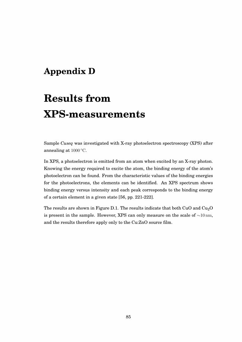
Appendix D
Results fromXPS-measurements
Sample Cuseq was investigated with X-ray photoelectron spectroscopy (XPS) after
annealing at 1000 C.
In XPS, a photoelectron is emitted from an atom when excited by an X-ray photon.
Knowing the energy required to excite the atom, the binding energy of the atom’s
photoelectron can be found. From the characteristic values of the binding energies
for the photoelectrons, the elements can be identified. An XPS spectrum shows
binding energy versus intensity and each peak corresponds to the binding energy
of a certain element in a given state [56, pp. 221-222].
The results are shown in Figure D.1. The results indicate that both CuO and Cu2O
is present in the sample. However, XPS can only measure on the scale of ∼10 nm,
and the results therefore apply only to the Cu:ZnO source film.
85
Appendix D. XPS-results 86
FIGURE D.1: XPS-spectra of Cu 2p for sample Cuseq annealed sequentially up to1000 C
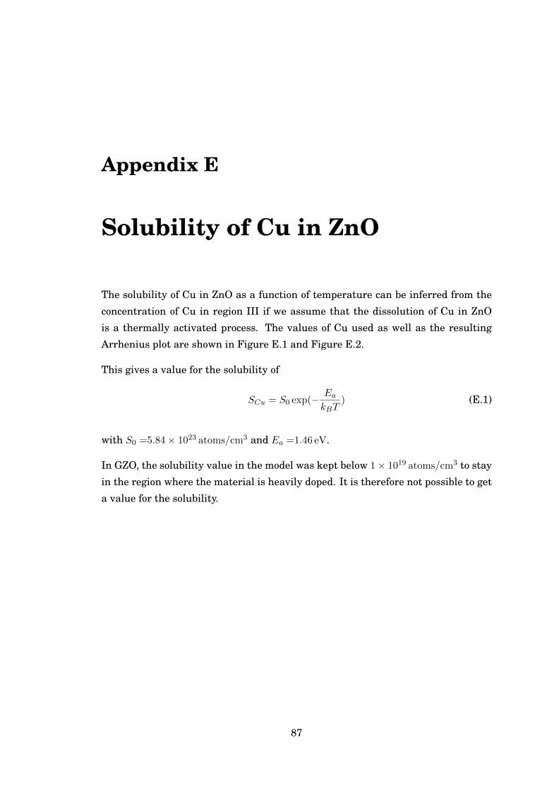
Appendix E
Solubility of Cu in ZnO
The solubility of Cu in ZnO as a function of temperature can be inferred from the
concentration of Cu in region III if we assume that the dissolution of Cu in ZnO
is a thermally activated process. The values of Cu used as well as the resulting
Arrhenius plot are shown in Figure E.1 and Figure E.2.
This gives a value for the solubility of
SCu = S0 exp(− EakBT
) (E.1)
with S0 =5.84× 10²³ atoms/cm3 and Ea =1.46 eV.
In GZO, the solubility value in the model was kept below 1× 10¹⁹ atoms/cm3 to stay
in the region where the material is heavily doped. It is therefore not possible to get
a value for the solubility.
87
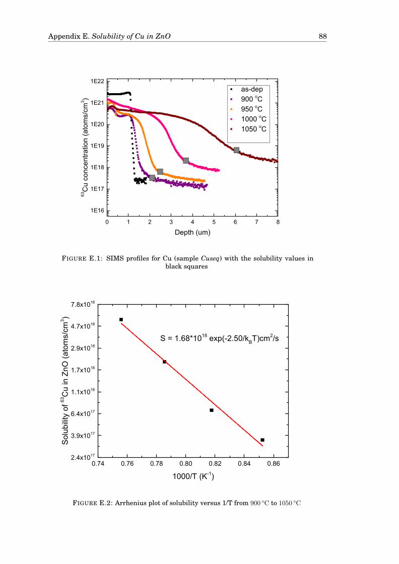
Appendix E. Solubility of Cu in ZnO 88
0 1 2 3 4 5 6 7 8
1E16
1E17
1E18
1E19
1E20
1E21
1E22 as-dep 900 oC 950 oC 1000 oC 1050 oC
63C
u co
ncen
tratio
n (a
tom
s/cm
3 )
Depth (um)
FIGURE E.1: SIMS profiles for Cu (sample Cuseq) with the solubility values inblack squares
0.74 0.76 0.78 0.80 0.82 0.84 0.862.4x1017
3.9x10¹⁷
6.4x10¹⁷
1.1x10¹⁸
1.7x10¹⁸
2.9x10¹⁸
4.7x10¹⁸
7.8x10¹⁸
S = 1.68*1018 exp(-2.50/kBT)cm2/s
Sol
ubilit
y of
63C
u in
ZnO
(ato
ms/
cm3 )
1000/T (K-1)
FIGURE E.2: Arrhenius plot of solubility versus 1/T from 900 C to 1050 C
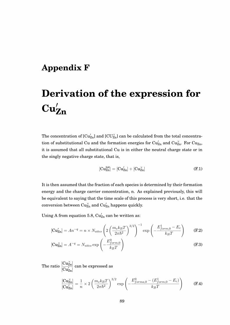
Appendix F
Derivation of the expression forCu′Zn
The concentration of [Cu′Zn] and [CU×Zn] can be calculated from the total concentra-
tion of substitutional Cu and the formation energies for Cu′Zn and Cu×Zn. For CuZn,
it is assumed that all substitutional Cu is in either the neutral charge state or in
the singly negative charge state, that is,
[CutotZn] = [Cu′Zn] + [Cu×Zn] (F.1)
It is then assumed that the fraction of each species is determined by their formation
energy and the charge carrier concentration, n. As explained previously, this will
be equivalent to saying that the time scale of this process is very short, i.e. that the
conversion between Cu×Zn and Cu′Zn happens quickly.
Using A from equation 5.8, Cu′Zn can be written as:
[Cu′Zn] = An−q = n×Nsites
(2
(mekBT
2π~2
)3/2)−1
exp
(−E1form,0 − EckBT
)(F.2)
[Cu×Zn] = A−q = Nsites exp
(−E0form,0
kBT
)(F.3)
The ratio[Cu×Zn]
[Cu′Zn]can be expressed as
[Cu×Zn]
[Cu′Zn]=
1
n× 2
(mekBT
2π~2
)3/2
exp
(−E0forma,0 − (E1
form,0 − Ec)kBT
)(F.4)
89
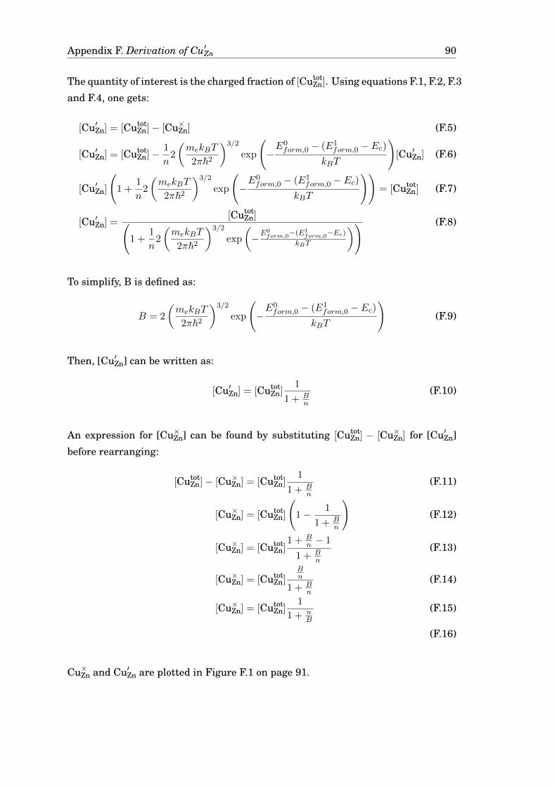
Appendix F. Derivation of Cu′Zn 90
The quantity of interest is the charged fraction of [CutotZn]. Using equations F.1, F.2, F.3
and F.4, one gets:
[Cu′Zn] = [CutotZn]− [Cu×Zn] (F.5)
[Cu′Zn] = [CutotZn]− 1
n2
(mekBT
2π~2
)3/2
exp
(−E0form,0 − (E1
form,0 − Ec)kBT
)[Cu′Zn] (F.6)
[Cu′Zn]
(1 +
1
n2
(mekBT
2π~2
)3/2
exp
(−E0form,0 − (E1
form,0 − Ec)kBT
))= [Cutot
Zn] (F.7)
[Cu′Zn] =[Cutot
Zn](1 +
1
n2
(mekBT
2π~2
)3/2
exp
(−E0
form,0−(E1form,0−Ec)
kBT
)) (F.8)
To simplify, B is defined as:
B = 2
(mekBT
2π~2
)3/2
exp
(−E0form,0 − (E1
form,0 − Ec)kBT
)(F.9)
Then, [Cu′Zn] can be written as:
[Cu′Zn] = [CutotZn]
1
1 + Bn
(F.10)
An expression for [Cu×Zn] can be found by substituting [CutotZn] − [Cu×Zn] for [Cu′Zn]
before rearranging:
[CutotZn]− [Cu×Zn] = [Cutot
Zn]1
1 + Bn
(F.11)
[Cu×Zn] = [CutotZn]
(1− 1
1 + Bn
)(F.12)
[Cu×Zn] = [CutotZn]
1 + Bn − 1
1 + Bn
(F.13)
[Cu×Zn] = [CutotZn]
Bn
1 + Bn
(F.14)
[Cu×Zn] = [CutotZn]
1
1 + nB
(F.15)
(F.16)
Cu×Zn and Cu′Zn are plotted in Figure F.1 on page 91.
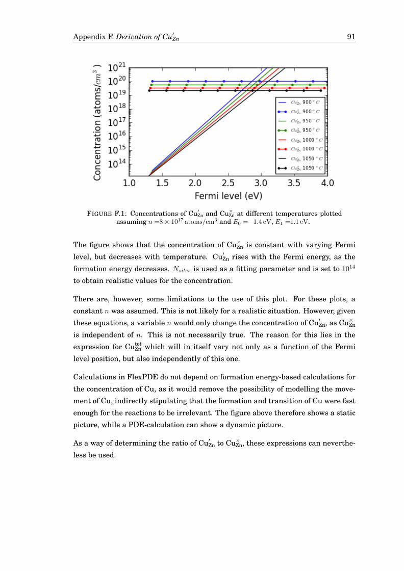
Appendix F. Derivation of Cu′Zn 91
FIGURE F.1: Concentrations of Cu′Zn and Cu×Zn at different temperatures plottedassuming n =8× 10¹⁷ atoms/cm3 and E0 =−1.4 eV, E1 =1.1 eV.
The figure shows that the concentration of Cu×Zn is constant with varying Fermi
level, but decreases with temperature. Cu′Zn rises with the Fermi energy, as the
formation energy decreases. Nsites is used as a fitting parameter and is set to 1014
to obtain realistic values for the concentration.
There are, however, some limitations to the use of this plot. For these plots, a
constant n was assumed. This is not likely for a realistic situation. However, given
these equations, a variable n would only change the concentration of Cu′Zn, as Cu×Zn
is independent of n. This is not necessarily true. The reason for this lies in the
expression for CutotZn which will in itself vary not only as a function of the Fermi
level position, but also independently of this one.
Calculations in FlexPDE do not depend on formation energy-based calculations for
the concentration of Cu, as it would remove the possibility of modelling the move-
ment of Cu, indirectly stipulating that the formation and transition of Cu were fast
enough for the reactions to be irrelevant. The figure above therefore shows a static
picture, while a PDE-calculation can show a dynamic picture.
As a way of determining the ratio of Cu′Zn to Cu×Zn, these expressions can neverthe-
less be used.

Bibliography
[1] Nobelprize.org. The Nobel Prize in Physics 2014. Web. Sept. 7, 2015. URL:
http://www.nobelprize.org/nobel_prizes/physics/laureates/2014/.
[2] The International Energy Agency. Topic: Energy poverty. Web. Sept. 7, 2015.
URL: http://www.iea.org/topics/energypoverty/.
[3] Climate Change 2014: Synthesis Report. Contribution of Working Groups I,II and III to the Fifth Assessment Report of the Intergovernmental Panel ofClimate Change. IPCC, Geneva, Switzerland, 2014.
[4] Ü. Özgür et al. ‘A comprehensive review of ZnO materials and devices’. In:
Journal of Applied Physics 98.4 (Aug. 2005), p. 041301.
[5] K. Ellmer. ‘Electrical Properties’. In: Transparent Conductive Zinc Oxide. Ed.
by D. K. Ellmer, D. A. Klein, and P. D. B. Rech. Springer Series in Materials
Science 104. DOI: 10.1007/978-3-540-73612-7_2. Springer Berlin Heidelberg,
2008, pp. 35–78.
[6] S. Nakamura et al. ‘Hole Compensation Mechanism of P-Type GaN Films’. In:
Japanese Journal of Applied Physics 31.Part 1, No. 5A (May 1992), pp. 1258–
1266.
[7] H. Amano et al. ‘P-Type Conduction in Mg-Doped GaN Treated with Low-
Energy Electron Beam Irradiation (LEEBI)’. In: Japanese Journal of AppliedPhysics 28.Part 2, No. 12 (Dec. 1989), pp. L2112–L2114.
[8] J. I. Pankove et al. ‘Neutralization of Shallow Acceptor Levels in Silicon by
Atomic Hydrogen’. In: Physical Review Letters 51.24 (Dec. 1983), pp. 2224–
2225.
[9] Merriam-Webster, ed. "diffusion". Sept. 2015.
[10] M. Gabás et al. ‘Electronic structure of Al- and Ga-doped ZnO films studied
by hard X-ray photoelectron spectroscopy’. In: APL Materials 2.1 (Jan. 2014),
p. 012112.
93
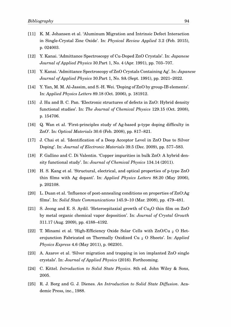
Bibliography 94
[11] K. M. Johansen et al. ‘Aluminum Migration and Intrinsic Defect Interaction
in Single-Crystal Zinc Oxide’. In: Physical Review Applied 3.2 (Feb. 2015),
p. 024003.
[12] Y. Kanai. ‘Admittance Spectroscopy of Cu-Doped ZnO Crystals’. In: JapaneseJournal of Applied Physics 30.Part 1, No. 4 (Apr. 1991), pp. 703–707.
[13] Y. Kanai. ‘Admittance Spectroscopy of ZnO Crystals Containing Ag’. In: JapaneseJournal of Applied Physics 30.Part 1, No. 9A (Sept. 1991), pp. 2021–2022.
[14] Y. Yan, M. M. Al-Jassim, and S.-H. Wei. ‘Doping of ZnO by group-IB elements’.
In: Applied Physics Letters 89.18 (Oct. 2006), p. 181912.
[15] J. Hu and B. C. Pan. ‘Electronic structures of defects in ZnO: Hybrid density
functional studies’. In: The Journal of Chemical Physics 129.15 (Oct. 2008),
p. 154706.
[16] Q. Wan et al. ‘First-principles study of Ag-based p-type doping difficulty in
ZnO’. In: Optical Materials 30.6 (Feb. 2008), pp. 817–821.
[17] J. Chai et al. ‘Identification of a Deep Acceptor Level in ZnO Due to Silver
Doping’. In: Journal of Electronic Materials 39.5 (Dec. 2009), pp. 577–583.
[18] F. Gallino and C. Di Valentin. ‘Copper impurities in bulk ZnO: A hybrid den-
sity functional study’. In: Journal of Chemical Physics 134.14 (2011).
[19] H. S. Kang et al. ‘Structural, electrical, and optical properties of p-type ZnO
thin films with Ag dopant’. In: Applied Physics Letters 88.20 (May 2006),
p. 202108.
[20] L. Duan et al. ‘Influence of post-annealing conditions on properties of ZnO:Ag
films’. In: Solid State Communications 145.9–10 (Mar. 2008), pp. 479–481.
[21] S. Jeong and E. S. Aydil. ‘Heteroepitaxial growth of Cu2O thin film on ZnO
by metal organic chemical vapor deposition’. In: Journal of Crystal Growth311.17 (Aug. 2009), pp. 4188–4192.
[22] T. Minami et al. ‘High-Efficiency Oxide Solar Cells with ZnO/Cu 2 O Het-
erojunction Fabricated on Thermally Oxidized Cu 2 O Sheets’. In: AppliedPhysics Express 4.6 (May 2011), p. 062301.
[23] A. Azarov et al. ‘Silver migration and trapping in ion implanted ZnO single
crystals’. In: Journal of Applied Physics (2016). Forthcoming.
[24] C. Kittel. Introduction to Solid State Physics. 8th ed. John Wiley & Sons,
2005.
[25] R. J. Borg and G. J. Dienes. An Introduction to Solid State Diffusion. Aca-
demic Press, inc., 1988.
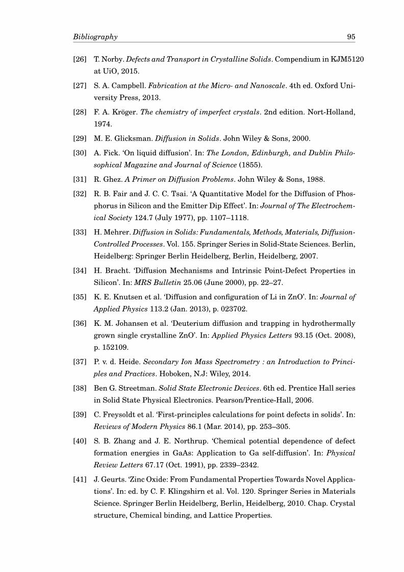
Bibliography 95
[26] T. Norby. Defects and Transport in Crystalline Solids. Compendium in KJM5120
at UiO, 2015.
[27] S. A. Campbell. Fabrication at the Micro- and Nanoscale. 4th ed. Oxford Uni-
versity Press, 2013.
[28] F. A. Kröger. The chemistry of imperfect crystals. 2nd edition. Nort-Holland,
1974.
[29] M. E. Glicksman. Diffusion in Solids. John Wiley & Sons, 2000.
[30] A. Fick. ‘On liquid diffusion’. In: The London, Edinburgh, and Dublin Philo-sophical Magazine and Journal of Science (1855).
[31] R. Ghez. A Primer on Diffusion Problems. John Wiley & Sons, 1988.
[32] R. B. Fair and J. C. C. Tsai. ‘A Quantitative Model for the Diffusion of Phos-
phorus in Silicon and the Emitter Dip Effect’. In: Journal of The Electrochem-ical Society 124.7 (July 1977), pp. 1107–1118.
[33] H. Mehrer. Diffusion in Solids: Fundamentals, Methods, Materials, Diffusion-Controlled Processes. Vol. 155. Springer Series in Solid-State Sciences. Berlin,
Heidelberg: Springer Berlin Heidelberg, Berlin, Heidelberg, 2007.
[34] H. Bracht. ‘Diffusion Mechanisms and Intrinsic Point-Defect Properties in
Silicon’. In: MRS Bulletin 25.06 (June 2000), pp. 22–27.
[35] K. E. Knutsen et al. ‘Diffusion and configuration of Li in ZnO’. In: Journal ofApplied Physics 113.2 (Jan. 2013), p. 023702.
[36] K. M. Johansen et al. ‘Deuterium diffusion and trapping in hydrothermally
grown single crystalline ZnO’. In: Applied Physics Letters 93.15 (Oct. 2008),
p. 152109.
[37] P. v. d. Heide. Secondary Ion Mass Spectrometry : an Introduction to Princi-ples and Practices. Hoboken, N.J: Wiley, 2014.
[38] Ben G. Streetman. Solid State Electronic Devices. 6th ed. Prentice Hall series
in Solid State Physical Electronics. Pearson/Prentice-Hall, 2006.
[39] C. Freysoldt et al. ‘First-principles calculations for point defects in solids’. In:
Reviews of Modern Physics 86.1 (Mar. 2014), pp. 253–305.
[40] S. B. Zhang and J. E. Northrup. ‘Chemical potential dependence of defect
formation energies in GaAs: Application to Ga self-diffusion’. In: PhysicalReview Letters 67.17 (Oct. 1991), pp. 2339–2342.
[41] J. Geurts. ‘Zinc Oxide: From Fundamental Properties Towards Novel Applica-
tions’. In: ed. by C. F. Klingshirn et al. Vol. 120. Springer Series in Materials
Science. Springer Berlin Heidelberg, Berlin, Heidelberg, 2010. Chap. Crystal
structure, Chemical binding, and Lattice Properties.
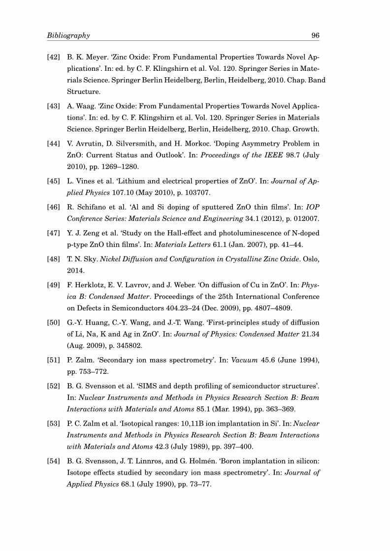
Bibliography 96
[42] B. K. Meyer. ‘Zinc Oxide: From Fundamental Properties Towards Novel Ap-
plications’. In: ed. by C. F. Klingshirn et al. Vol. 120. Springer Series in Mate-
rials Science. Springer Berlin Heidelberg, Berlin, Heidelberg, 2010. Chap. Band
Structure.
[43] A. Waag. ‘Zinc Oxide: From Fundamental Properties Towards Novel Applica-
tions’. In: ed. by C. F. Klingshirn et al. Vol. 120. Springer Series in Materials
Science. Springer Berlin Heidelberg, Berlin, Heidelberg, 2010. Chap. Growth.
[44] V. Avrutin, D. Silversmith, and H. Morkoc. ‘Doping Asymmetry Problem in
ZnO: Current Status and Outlook’. In: Proceedings of the IEEE 98.7 (July
2010), pp. 1269–1280.
[45] L. Vines et al. ‘Lithium and electrical properties of ZnO’. In: Journal of Ap-plied Physics 107.10 (May 2010), p. 103707.
[46] R. Schifano et al. ‘Al and Si doping of sputtered ZnO thin films’. In: IOPConference Series: Materials Science and Engineering 34.1 (2012), p. 012007.
[47] Y. J. Zeng et al. ‘Study on the Hall-effect and photoluminescence of N-doped
p-type ZnO thin films’. In: Materials Letters 61.1 (Jan. 2007), pp. 41–44.
[48] T. N. Sky. Nickel Diffusion and Configuration in Crystalline Zinc Oxide. Oslo,
2014.
[49] F. Herklotz, E. V. Lavrov, and J. Weber. ‘On diffusion of Cu in ZnO’. In: Phys-ica B: Condensed Matter. Proceedings of the 25th International Conference
on Defects in Semiconductors 404.23–24 (Dec. 2009), pp. 4807–4809.
[50] G.-Y. Huang, C.-Y. Wang, and J.-T. Wang. ‘First-principles study of diffusion
of Li, Na, K and Ag in ZnO’. In: Journal of Physics: Condensed Matter 21.34
(Aug. 2009), p. 345802.
[51] P. Zalm. ‘Secondary ion mass spectrometry’. In: Vacuum 45.6 (June 1994),
pp. 753–772.
[52] B. G. Svensson et al. ‘SIMS and depth profiling of semiconductor structures’.
In: Nuclear Instruments and Methods in Physics Research Section B: BeamInteractions with Materials and Atoms 85.1 (Mar. 1994), pp. 363–369.
[53] P. C. Zalm et al. ‘Isotopical ranges: 10,11B ion implantation in Si’. In: NuclearInstruments and Methods in Physics Research Section B: Beam Interactionswith Materials and Atoms 42.3 (July 1989), pp. 397–400.
[54] B. G. Svensson, J. T. Linnros, and G. Holmén. ‘Boron implantation in silicon:
Isotope effects studied by secondary ion mass spectrometry’. In: Journal ofApplied Physics 68.1 (July 1990), pp. 73–77.
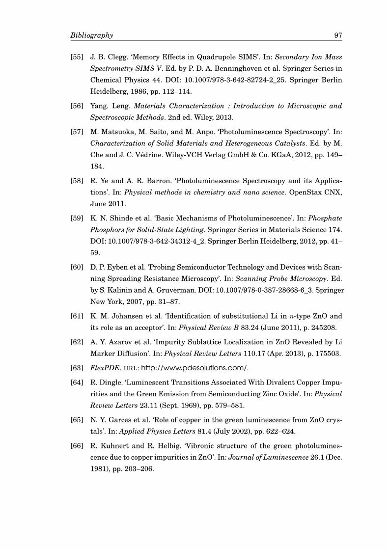
Bibliography 97
[55] J. B. Clegg. ‘Memory Effects in Quadrupole SIMS’. In: Secondary Ion MassSpectrometry SIMS V. Ed. by P. D. A. Benninghoven et al. Springer Series in
Chemical Physics 44. DOI: 10.1007/978-3-642-82724-2_25. Springer Berlin
Heidelberg, 1986, pp. 112–114.
[56] Yang. Leng. Materials Characterization : Introduction to Microscopic andSpectroscopic Methods. 2nd ed. Wiley, 2013.
[57] M. Matsuoka, M. Saito, and M. Anpo. ‘Photoluminescence Spectroscopy’. In:
Characterization of Solid Materials and Heterogeneous Catalysts. Ed. by M.
Che and J. C. Védrine. Wiley-VCH Verlag GmbH & Co. KGaA, 2012, pp. 149–
184.
[58] R. Ye and A. R. Barron. ‘Photoluminescence Spectroscopy and its Applica-
tions’. In: Physical methods in chemistry and nano science. OpenStax CNX,
June 2011.
[59] K. N. Shinde et al. ‘Basic Mechanisms of Photoluminescence’. In: PhosphatePhosphors for Solid-State Lighting. Springer Series in Materials Science 174.
DOI: 10.1007/978-3-642-34312-4_2. Springer Berlin Heidelberg, 2012, pp. 41–
59.
[60] D. P. Eyben et al. ‘Probing Semiconductor Technology and Devices with Scan-
ning Spreading Resistance Microscopy’. In: Scanning Probe Microscopy. Ed.
by S. Kalinin and A. Gruverman. DOI: 10.1007/978-0-387-28668-6_3. Springer
New York, 2007, pp. 31–87.
[61] K. M. Johansen et al. ‘Identification of substitutional Li in n-type ZnO and
its role as an acceptor’. In: Physical Review B 83.24 (June 2011), p. 245208.
[62] A. Y. Azarov et al. ‘Impurity Sublattice Localization in ZnO Revealed by Li
Marker Diffusion’. In: Physical Review Letters 110.17 (Apr. 2013), p. 175503.
[63] FlexPDE. URL: http://www.pdesolutions.com/.
[64] R. Dingle. ‘Luminescent Transitions Associated With Divalent Copper Impu-
rities and the Green Emission from Semiconducting Zinc Oxide’. In: PhysicalReview Letters 23.11 (Sept. 1969), pp. 579–581.
[65] N. Y. Garces et al. ‘Role of copper in the green luminescence from ZnO crys-
tals’. In: Applied Physics Letters 81.4 (July 2002), pp. 622–624.
[66] R. Kuhnert and R. Helbig. ‘Vibronic structure of the green photolumines-
cence due to copper impurities in ZnO’. In: Journal of Luminescence 26.1 (Dec.
1981), pp. 203–206.
Bibliography 98
[67] F. Leiter et al. ‘Magnetic resonance experiments on the green emission in
undoped ZnO crystals’. In: Physica B: Condensed Matter. International Con-
ference on Defects in Semiconductors 308–310 (Dec. 2001), pp. 908–911.
[68] D. Byrne et al. ‘Unambiguous identification of the role of a single Cu atom in
the ZnO structured green band’. en. In: Journal of Physics: Condensed Matter24.21 (2012), p. 215802.
[69] K. E. Knutsen et al. ‘Zinc vacancy and oxygen interstitial in ZnO revealed by
sequential annealing and electron irradiation’. In: Physical Review B 86.12
(Sept. 2012), p. 121203.
[70] Y. Dong et al. ‘Vacancy defect and defect cluster energetics in ion-implanted
ZnO’. In: Physical Review B 81.8 (Feb. 2010), p. 081201.
[71] L. De Los Santos Valladares et al. ‘Crystallization and electrical resistiv-
ity of Cu2O and CuO obtained by thermal oxidation of Cu thin films on
chSiO2/Sisubstrates’. In: Thin Solid Films 520.20 (Aug. 2012), pp. 6368–6374.
[72] L. Xia, Z. Liu, and P. A. Taskinen. ‘Phase equilibria study of Cu–O–ZnO
system in various oxygen partial pressures’. In: Ceramics International 42.4
(Mar. 2016), pp. 5418–5426.
[73] A. Laufer et al. ‘Determination of secondary ion mass spectrometry rela-
tive sensitivity factors for polar and non-polar ZnO’. In: Journal of AppliedPhysics 110.9 (Nov. 2011), p. 094906.
[74] A. Laufer et al. ‘Quantification of impurity concentration in Cu2O and CuO
via secondary ion mass spectrometry’. In: physica status solidi (b) 249.4 (Apr.
2012), pp. 801–811.
[75] K. Ellmer and A. Klein. ‘ZnO and Its Applications’. In: Transparent Conduc-tive Zinc Oxide. Ed. by D. K. Ellmer, D. A. Klein, and P. D. B. Rech. Springer
Series in Materials Science 104. DOI: 10.1007/978-3-540-73612-7_1. Springer
Berlin Heidelberg, 2008, pp. 1–33.
[76] N. H. Nickel. ‘Hydrogen migration in single crystal and polycrystalline zinc
oxide’. In: Physical Review B 73.19 (May 2006), p. 195204.
[77] M. S. Janson et al. ‘Hydrogen diffusion, complex formation, and dissociation
in acceptor-doped silicon carbide’. In: Physical Review B 64.19 (Oct. 2001),
p. 195202.
[78] D. Steiauf et al. ‘First-principles study of vacancy-assisted impurity diffusion
in ZnO’. In: APL Materials 2.9 (Sept. 2014), p. 096101.
[79] M. Berglund and M. E. Wieser. ‘Isotopic compositions of the elements 2009
(IUPAC Technical Report)’. In: Pure and Applied Chemistry 83.2 (Jan. 2011).