Embed Size (px)
Citation preview

Dye and Pry of BGA Solder Joints
www.cascade-eng.com
Reliability Engineering GroupCascade Engineering Services, Inc.
6640 185th Ave NE Redmond WA 98052(425) 895-8617 x 564
CPU Failure InvestigationEquipment Used
• Dye and Pry Technique
Conclusions• Majority of failures (cracks from mechanical bend overstress test) observed at Solder-Chip interface
• Summary of % area cracked at each interface in the area of interest
Optical Image with Extended Focal Imaging Stitching
Solder-ChipOk
Solder-PCBOk
Solder-PCBOk
Solder-PCBOk
Solder-Chip~5%
Solder-ChipOk
Solder-PCBOk
Solder-PCBOk
Solder-PCBOk
Solder-PCBOk
Solder-Chip~10%
Solder-PCBOk
Solder-PCBOk
Solder-PCBOk
Solder-Chip~20%
Solder-PCBOk
Chip PCB
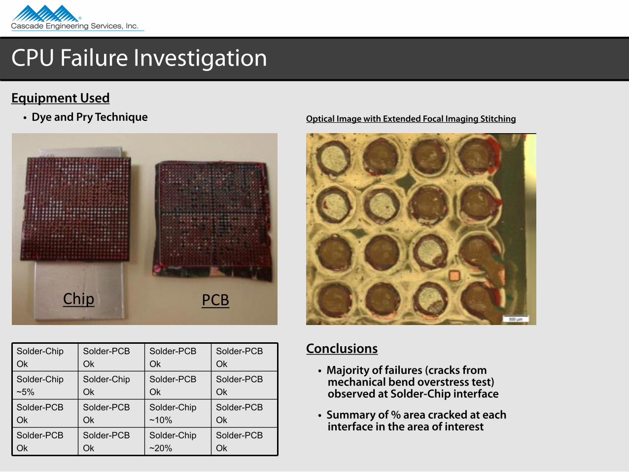
DRAM Failure InvestigationEquipment Used
• Dye and Pry Technique
Conclusions• Interfacial fracture / cracks observed at two locations: Solder-CU-PCB Interface and Solder Chip interface
• Summary of % area cracked at each interface in the area of interest
Chip PCB
Solder-chip~80%
Solder-PCB~50%
Solder-chip~5%
Solder-chip~50%
Solder-PCB~40%
Solder-PCB~50%
Solder-chip~50%
Solder-chip~15%
Solder-Chip~10%
Solder-chip
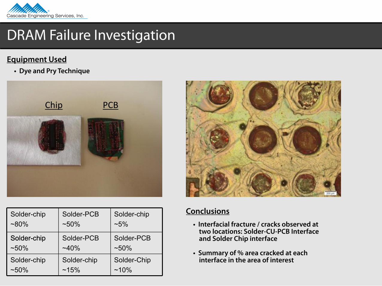
DRAM Failure Investigation (Continued)Equipment Used
• Dye and Pry Technique
Chip PCB
Images show the fracture surface after three point bending test.Presence of red dye indicates cracks in the area of interest
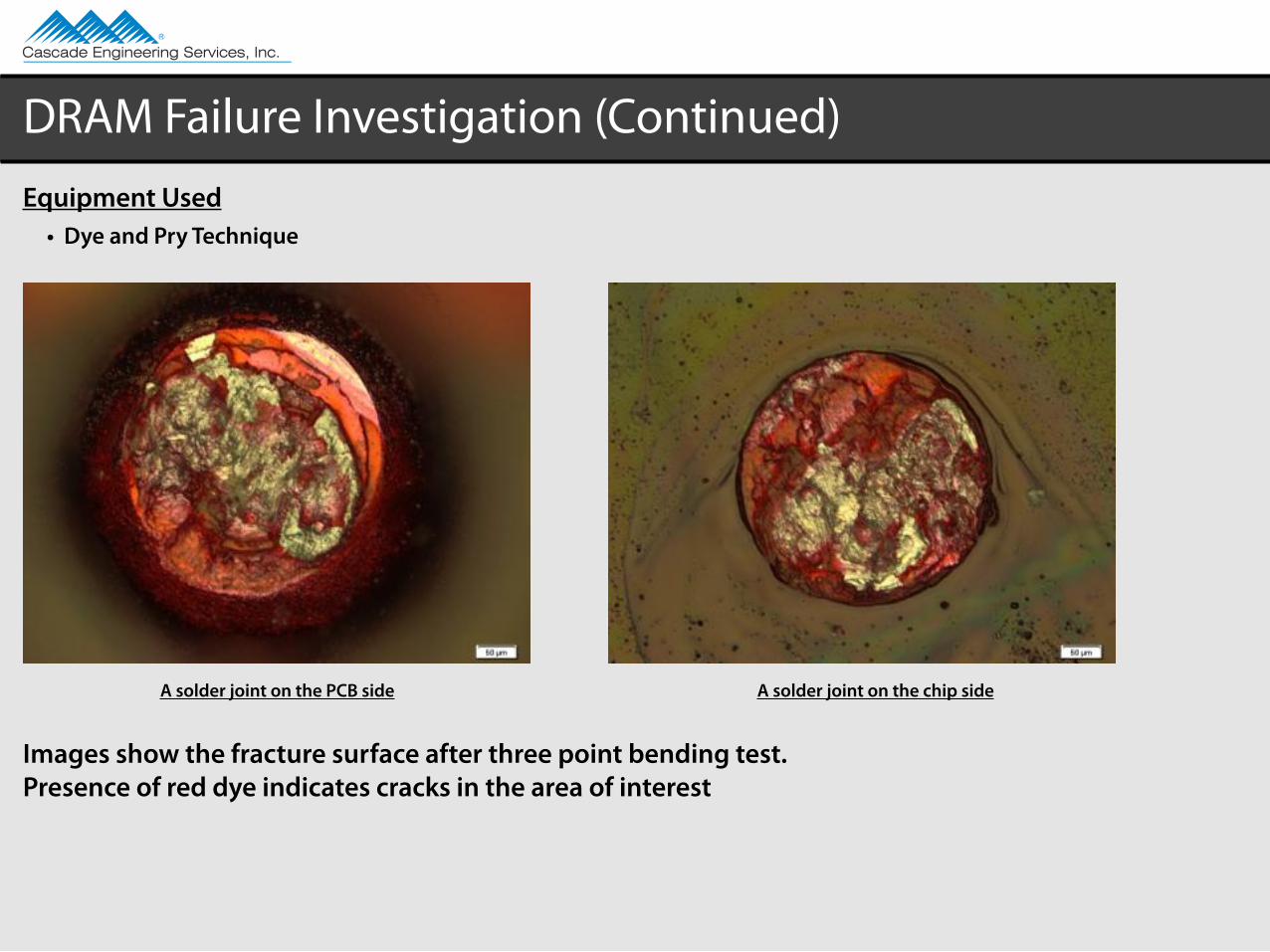
DRAM Failure Investigation (Continued)Equipment Used
• Dye and Pry Technique
Images show the fracture surface after three point bending test.Presence of red dye indicates cracks in the area of interest
A solder joint on the PCB side A solder joint on the chip side