Embed Size (px)
Citation preview

EMCA mini project report
The operational amplifier
PORAUDEAU Thomas
RANQUE Antony
25/01/2013

Antony RANQUE & Thomas POIRAUDEAU 4A – AE SE1 EMCA Report
2 INSA Toulouse – January 2013
Table of Contents Table of Contents ............................................................................................................................... 2
Introduction ....................................................................................................................................... 3
I. Studying the Op-Amp by itself ............................................................................................... 3
II. Op-Amp in voltage follower configuration ............................................................................ 4
1) The simple voltage follower ........................................................................................... 5
2) The voltage follower with a bias ..................................................................................... 6
3) Differential voltage follower amplifier ........................................................................... 7
4) Partial conclusion ............................................................................................................ 8
III. Op-Amp in comparator configuration ................................................................................... 9
1) Comparator with a bias .................................................................................................. 9
2) Differential comparator ................................................................................................ 10
3) Partial conclusion .......................................................................................................... 11
IV. Op-Amp in electronic circuits ........................................................................................... 11
1) The integrator ............................................................................................................... 11
2) The inverting amplifier.................................................................................................. 12
3) The inverting summing amplifier .................................................................................. 14
Conclusion ........................................................................................................................................ 15
Table of Figures ................................................................................................................................ 16
BIBLIOGRAPHY ................................................................................................................................. 17

Antony RANQUE & Thomas POIRAUDEAU 4A – AE SE1 EMCA Report
3 INSA Toulouse – January 2013
Introduction As a follow-up to the EMCA (Modeling Active Components) course, it is suggested to us
to work on a mini-project and provide a report of it after 3 workshops. We decided to study
the operational amplifier and to work on simple circuits using it.
The operational Amplifier (also called Op-Amp, see Figure 1) is an active electronic
component useful for a great number of applications. It produces an output voltage that is
the difference between the two input terminals, multiplied by a gain A.
Figure 1 : Operational Amplifier basic drawing
The main objective of this report is to understand the structure and the behavior of a
simple Op-Amp, then to understand how it is used in simple circuits (ex: follower) and how it
can work properly. Our work is mainly based on design and simulation by MicroWind
software.
I. Studying the Op-Amp by itself The internal structure of an operational amplifier depends on the performances
expected and the way that component will be used. In this work, we decided to start from
the simplest architecture quickly to focus on the study of Op-Amp circuits.
This architecture is using two pMOS and two nMOS (see Figure 2). The principle is very
simple: When V+ = V-, no current go in the output and Vout = Vref. But when there’s a
variation of the potential V+ or V- the current difference between goes in the output and
Vout vary until the current reach the same value in both branches.
Figure 2 : Schematic diagram of the simplest architecture of the Op-Amp
Antony RANQUE & Thomas POIRAUDEAU 4A – AE SE1 EMCA Report
4 INSA Toulouse – January 2013
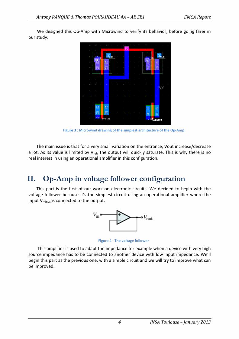
We designed this Op-Amp with Microwind to verify its behavior, before going farer in
our study:
Figure 3 : Microwind drawing of the simplest architecture of the Op-Amp
The main issue is that for a very small variation on the entrance, Vout increase/decrease
a lot. As its value is limited by Vref, the output will quickly saturate. This is why there is no
real interest in using an operational amplifier in this configuration.
II. Op-Amp in voltage follower configuration This part is the first of our work on electronic circuits. We decided to begin with the
voltage follower because it’s the simplest circuit using an operational amplifier where the
input Vminus is connected to the output.
Figure 4 : The voltage follower
This amplifier is used to adapt the impedance for example when a device with very high
source impedance has to be connected to another device with low input impedance. We’ll
begin this part as the previous one, with a simple circuit and we will try to improve what can
be improved.

Antony RANQUE & Thomas POIRAUDEAU 4A – AE SE1 EMCA Report
5 INSA Toulouse – January 2013
1) The simple voltage follower
We just connected the output on V- input and put our signal on the V+ input:
Figure 5 : Microwind drawing of the simple voltage follower
By simulating this, we expected to see the output following our signal on V+. The next
figure shows the result of our simulation.
Figure 6 : Simulation of the simple voltage follower
We can see that the result is not what we expected. The output signal (red curve) is not
following properly for voltages more than 1V on V+. We must improve it for higher
potentials on V+ input.

Antony RANQUE & Thomas POIRAUDEAU 4A – AE SE1 EMCA Report
6 INSA Toulouse – January 2013
2) The voltage follower with a bias
We decided to replace the Op-Amp we used by an operational amplifier with a bias as
shown on the next figure:
Figure 7 : Operational amplifier with a bias
This input Vbias allow to drive the current variation in both branches and by doing so
allow the circuit to work properly with a lower voltage to avoid saturation effects. We
decided to try this solution with Microwind :
Figure 8 : Microwind drawing of a voltage follower with bias
With this change we should have better results for a larger voltage range on V+ input.
We decided to try three different values for Vbias and we found out that the best
performances are fort Vbias=0.2V:
Figure 9 : Results of the voltage follower with bias simulation
Antony RANQUE & Thomas POIRAUDEAU 4A – AE SE1 EMCA Report
7 INSA Toulouse – January 2013
In our case, we can see that for a bias less than 0.2V, the output cannot follow the V+
input and has a behavior near a capacitor’s one. With a bias higher than 0.2V the output
cannot follow the input for high positive voltage.
For all the values of Vbias, we can see that we still have a bad following behavior in
negative voltages. So we had the idea to try the same circuit but with the bias at the top of
the branches like shown in the next figure:
Figure 10 : Operational amplifier with a bias (mirror)
We did exactly the same simulations for this circuit and we figure out that the results
were the opposite (good following for negative voltages but bad one for positive voltages).
The best value of the bias is still 0.2V.
Our last solution is to combine these two previous circuits, putting a bias both at the top
and at the bottom of the branches.
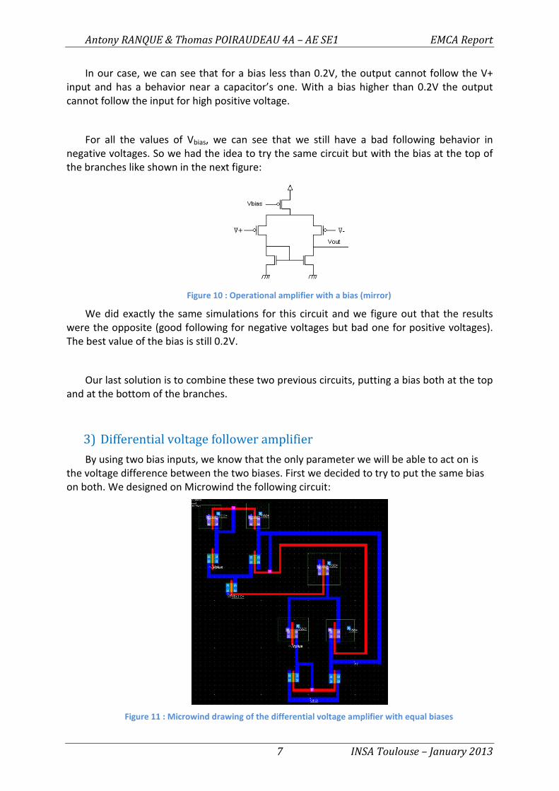
3) Differential voltage follower amplifier
By using two bias inputs, we know that the only parameter we will be able to act on is
the voltage difference between the two biases. First we decided to try to put the same bias
on both. We designed on Microwind the following circuit:
Figure 11 : Microwind drawing of the differential voltage amplifier with equal biases

Antony RANQUE & Thomas POIRAUDEAU 4A – AE SE1 EMCA Report
8 INSA Toulouse – January 2013
We obtained good results but that still can be improved:
Figure 12 : Simulation of the differential voltage follower amplifier (equal biases)
The solution can be to softly increase the difference between the two bias voltages, we
modified our drawing on Microwind and we simulated once again to obtain a very satisfying
result:
Figure 13 : Simulation of the differential voltage follower amplifier (different biases)
4) Partial conclusion
Finally by modifying our model of the operational amplifier, we found a way to design a
voltage follower with a great behavior. It would be interesting to try the same approach for a
different circuit to see if the differential operational amplifier with two bias at different
voltage is in all configuration the best solution to choose.

Antony RANQUE & Thomas POIRAUDEAU 4A – AE SE1 EMCA Report
9 INSA Toulouse – January 2013
III. Op-Amp in comparator configuration We decided to work on the comparator to verify our previous hypothesis. The
comparator indicates which of the two inputs has a higher voltage. The output should be, in
our case, equals to Vref when Vplus is higher than Vminus and equals to zero when Vplus is lower
than Vminus. The next figure shows the basic drawing of a comparator :
Figure 14 : Comparator's basic drawing
We will follow the same steps to try to design an efficient comparator.
1) Comparator with a bias
As we quickly saw that the comparator using our simplest design of the Op-Amp was
really poor, we begin with the comparator using an operational amplifier with a bias (see
figure 7). Our Microwind drawing is shown on the next figure:
Figure 15 : Microwind drawing of a comparator with a bias
We decided to put a constant signal on V- and a sinus on V+ with an offset equals to V-
potential. The output should be 0 when the sinus is in a positive waveform and Vref instead.
The result of our first simulation is shown on the next figure.

Antony RANQUE & Thomas POIRAUDEAU 4A – AE SE1 EMCA Report
10 INSA Toulouse – January 2013
Figure 16 : Simulation of a comparator with a bias (0.2V)
The behavior of our comparator is good but we can see that when the output should be
equal to zero, the result is not as clear as when the output should be equal to 1.
After trying quickly to simulate a comparator with a mirror bias (see figure 10) we got an
opposite output waveform. We decided to try the last circuit, using two bias like in the
previous part.
2) Differential comparator
We decided to test the comparator using a differential operational amplifier. Our
Microwind design is shown on the next figure:
Figure 17 : Microwind drawing of the differential comparator (different biases)
Antony RANQUE & Thomas POIRAUDEAU 4A – AE SE1 EMCA Report
11 INSA Toulouse – January 2013
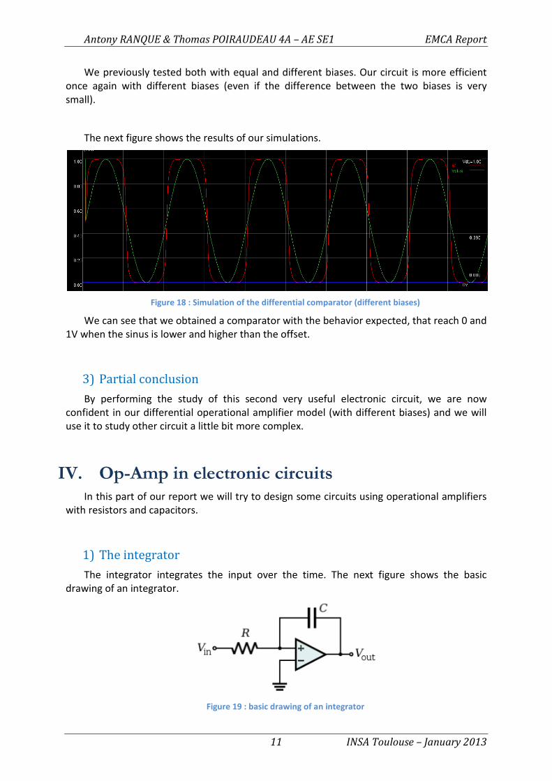
We previously tested both with equal and different biases. Our circuit is more efficient
once again with different biases (even if the difference between the two biases is very
small).
The next figure shows the results of our simulations.
Figure 18 : Simulation of the differential comparator (different biases)
We can see that we obtained a comparator with the behavior expected, that reach 0 and
1V when the sinus is lower and higher than the offset.
3) Partial conclusion
By performing the study of this second very useful electronic circuit, we are now
confident in our differential operational amplifier model (with different biases) and we will
use it to study other circuit a little bit more complex.
IV. Op-Amp in electronic circuits In this part of our report we will try to design some circuits using operational amplifiers
with resistors and capacitors.
1) The integrator
The integrator integrates the input over the time. The next figure shows the basic
drawing of an integrator.
Figure 19 : basic drawing of an integrator
Antony RANQUE & Thomas POIRAUDEAU 4A – AE SE1 EMCA Report
12 INSA Toulouse – January 2013
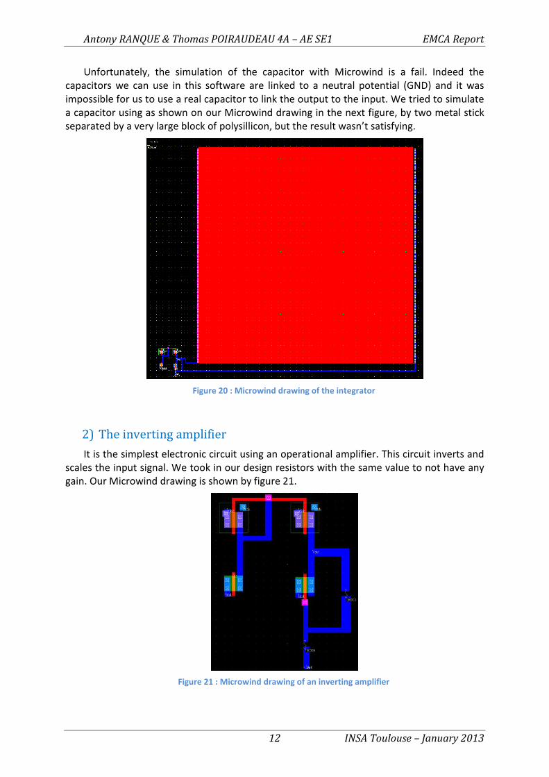
Unfortunately, the simulation of the capacitor with Microwind is a fail. Indeed the
capacitors we can use in this software are linked to a neutral potential (GND) and it was
impossible for us to use a real capacitor to link the output to the input. We tried to simulate
a capacitor using as shown on our Microwind drawing in the next figure, by two metal stick
separated by a very large block of polysillicon, but the result wasn’t satisfying.
Figure 20 : Microwind drawing of the integrator
2) The inverting amplifier
It is the simplest electronic circuit using an operational amplifier. This circuit inverts and
scales the input signal. We took in our design resistors with the same value to not have any
gain. Our Microwind drawing is shown by figure 21.
Figure 21 : Microwind drawing of an inverting amplifier

Antony RANQUE & Thomas POIRAUDEAU 4A – AE SE1 EMCA Report
13 INSA Toulouse – January 2013
Then we simulated it and we obtained very good results, the output is the opposite of
the input, and no gain is assumed. See figure 22.
Figure 22 : Simulation of the inverting amplifier (gain =1)

Antony RANQUE & Thomas POIRAUDEAU 4A – AE SE1 EMCA Report
14 INSA Toulouse – January 2013
3) The inverting summing amplifier
We decided to work a little bit more on our inverting amplifier by trying to design an
inverting summing amplifier. The output should be the opposite of the sum of all the input
voltages. Our Mircrowind drawing is shown on the next figure.
Figure 23 : Microwind drawing of a inverting summing amplifier
We chose to put all the resistors at the same value to have the output equals to the sum
of both the input signals but with an opposite sign. The result of our simulation is shown on
figure 24.
Figure 24 : Simulation of the inverting summing amplifier
We obtained the results expected.
We also tried to realize an inverting subtracting amplifier. As the design is barely the
same it won’t be detailed in this report but once again the results were very satisfying.

Antony RANQUE & Thomas POIRAUDEAU 4A – AE SE1 EMCA Report
15 INSA Toulouse – January 2013
Conclusion The operational amplifier is one of the most used component in electronic. This is why
we decided to work on it for this mini-project of the course “Modeling of Active
components”. We had the possibility to fully understand the behavior of this component, its
inside architecture as well as its different design with their good and weak points. Moreover
we successfully design basic circuits using Op-Amp.
During this work, we learned how to use Microwind, a design-software of basic
components. It was very interesting to have the possibility to simulate our designs and to try
solutions in order to solve our issues and to meet our objectives.

Antony RANQUE & Thomas POIRAUDEAU 4A – AE SE1 EMCA Report
16 INSA Toulouse – January 2013
Table of Figures
Figure 1 : Operational Amplifier basic drawing ................................................................... 3
Figure 2 : Schematic diagram of the simplest architecture of the Op-Amp........................ 3
Figure 3 : Microwind drawing of the simplest architecture of the Op-Amp ....................... 4
Figure 4 : The voltage follower ............................................................................................ 4
Figure 5 : Microwind drawing of the simple voltage follower ............................................ 5
Figure 6 : Simulation of the simple voltage follower ........................................................... 5
Figure 7 : Operational amplifier with a bias ........................................................................ 6
Figure 8 : Microwind drawing of a voltage follower with bias ............................................ 6
Figure 9 : Results of the voltage follower with bias simulation .......................................... 6
Figure 10 : Operational amplifier with a bias (mirror) ........................................................ 7
Figure 11 : Microwind drawing of the differential voltage amplifier with equal biases ..... 7
Figure 12 : Simulation of the differential voltage follower amplifier (equal biases) .......... 8
Figure 13 : Simulation of the differential voltage follower amplifier (different biases) ..... 8
Figure 14 : Comparator's basic drawing .............................................................................. 9
Figure 15 : Microwind drawing of a comparator with a bias .............................................. 9
Figure 16 : Simulation of a comparator with a bias (0.2V) ................................................ 10
Figure 17 : Microwind drawing of the differential comparator (different biases) ............ 10
Figure 18 : Simulation of the differential comparator (different biases) .......................... 11
Figure 19 : basic drawing of an integrator ......................................................................... 11
Figure 20 : Microwind drawing of the integrator .............................................................. 12
Figure 21 : Microwind drawing of an inverting amplifier .................................................. 12
Figure 22 : Simulation of the inverting amplifier (gain =1) ............................................... 13
Figure 23 : Microwind drawing of a inverting summing amplifier .................................... 14
Figure 24 : Simulation of the inverting summing amplifier ............................................... 14

Antony RANQUE & Thomas POIRAUDEAU 4A – AE SE1 EMCA Report
17 INSA Toulouse – January 2013
BIBLIOGRAPHY
Greg Kovas, Op-Amp_Concepts.pdf. Stanford University.
Etienne Sicard, Sonia Delmas Bendhia, Basics of CMOS Cell Design, 2007


![Tutorial_Manual Microwind 1.d[1]](https://img.pdfslide.net/doc/110x75/5540d36d4a7959f00c8b4b0f/tutorialmanual-microwind-1d1.jpg)