Embed Size (px)
Citation preview
EXPERIMENTAL EVALUATION OF LONG TERMEVOLUTION-BASED NC OFDM
SECONDARY-TO-SECONDARY INTERFERENCE
BY AJAY RAMKUMAR IYER
A thesis submitted to the
Graduate School—New Brunswick
Rutgers, The State University of New Jersey
in partial fulfillment of the requirements
for the degree of
Master of Science
Graduate Program in Electrical and Computer Engineering
Written under the direction of
Prof. Predrag Spasojevic
and approved by
New Brunswick, New Jersey
October, 2012

c© 2012
Ajay Ramkumar Iyer
ALL RIGHTS RESERVED

ABSTRACT OF THE THESIS
Experimental Evaluation of Long Term Evolution-Based
NC OFDM Secondary-to-Secondary Interference
by Ajay Ramkumar Iyer
Thesis Director: Prof. Predrag Spasojevic
Scarcity of spectrum resources, inefficient spectrum usage and the inflexibility of the
current spectrum assignment are few of the major roadblocks in the development of
new wireless communication standards. Secondary spectrum sharing has become a vi-
able solution to alleviate this problem. Secondary users are unlicensed devices that use
opportunistic spectrum access to identify vacant frequency bins and thereby utilize the
spectrum. For advanced wireless communication standards like the Long Term Evolu-
tion (LTE) which primarily calls for higher data rates, evaluation of design parameters
for ensuring efficient coexistence of heterogeneous secondary users and guaranteeing
acceptable minimum level of performance becomes essential. Additionally, the un-
derstanding of the interference between secondary users occupying adjacent frequency
bands for their transmission is imperative.
This thesis focuses on the coexistence of secondary users in the same band assuming
that the primary spectrum is found available. By implementing two Non Contiguous
Orthogonal Frequency Division Multiplexing ( NC-OFDM) based secondary transmit-
ters on a real time platform, the design parameters that need to be considered to ensure
efficient coexistence have been identified and investigated. The performance degrada-
tions observed at a particular secondary link due to presence of another interfering
ii
secondary link occupying adjacent frequency bands for its transmission have also been
studied. This thesis also focuses on implementation of algorithms to modify the exist-
ing NC-OFDM transmission at the secondary transmitter end to reduce its interference
effects on the other secondary links operating within the same band. The focus is on
an LTE-based Secondary Non Contiguous Orthogonal Frequency Division Multiplexing
Transceiver on a Real Time Platform developed by National Instruments . The various
blocks needed to design a real time LTE based communications links are discussed. An
experimental LTE-to-LTE interference analysis based on the Real Time Platform and
the designed system is presented.
iii
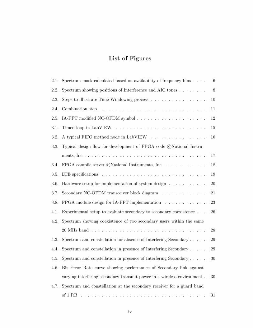
List of Figures
2.1. Spectrum mask calculated based on availability of frequency bins . . . . 6
2.2. Spectrum showing positions of Interference and AIC tones . . . . . . . . 8
2.3. Steps to illustrate Time Windowing process . . . . . . . . . . . . . . . . 10
2.4. Combination step . . . . . . . . . . . . . . . . . . . . . . . . . . . . . . . 11
2.5. IA-PFT modified NC-OFDM symbol . . . . . . . . . . . . . . . . . . . . 12
3.1. Timed loop in LabVIEW . . . . . . . . . . . . . . . . . . . . . . . . . . 15
3.2. A typical FIFO method node in LabVIEW . . . . . . . . . . . . . . . . 16
3.3. Typical design flow for development of FPGA code c©National Instru-
ments, Inc . . . . . . . . . . . . . . . . . . . . . . . . . . . . . . . . . . . 17
3.4. FPGA compile server c©National Instruments, Inc . . . . . . . . . . . . 18
3.5. LTE specifications . . . . . . . . . . . . . . . . . . . . . . . . . . . . . . 19
3.6. Hardware setup for implementation of system design . . . . . . . . . . . 20
3.7. Secondary NC-OFDM transceiver block diagram . . . . . . . . . . . . . 21
3.8. FPGA module design for IA-PFT implementation . . . . . . . . . . . . 23
4.1. Experimental setup to evaluate secondary to secondary coexistence . . . 26
4.2. Spectrum showing coexistence of two secondary users within the same
20 MHz band . . . . . . . . . . . . . . . . . . . . . . . . . . . . . . . . . 28
4.3. Spectrum and constellation for absence of Interfering Secondary . . . . . 29
4.4. Spectrum and constellation in presence of Interfering Secondary . . . . . 29
4.5. Spectrum and constellation in presence of Interfering Secondary . . . . . 30
4.6. Bit Error Rate curve showing performance of Secondary link against
varying interfering secondary transmit power in a wireless environment . 30
4.7. Spectrum and constellation at the secondary receiver for a guard band
of 1 RB . . . . . . . . . . . . . . . . . . . . . . . . . . . . . . . . . . . . 31
iv
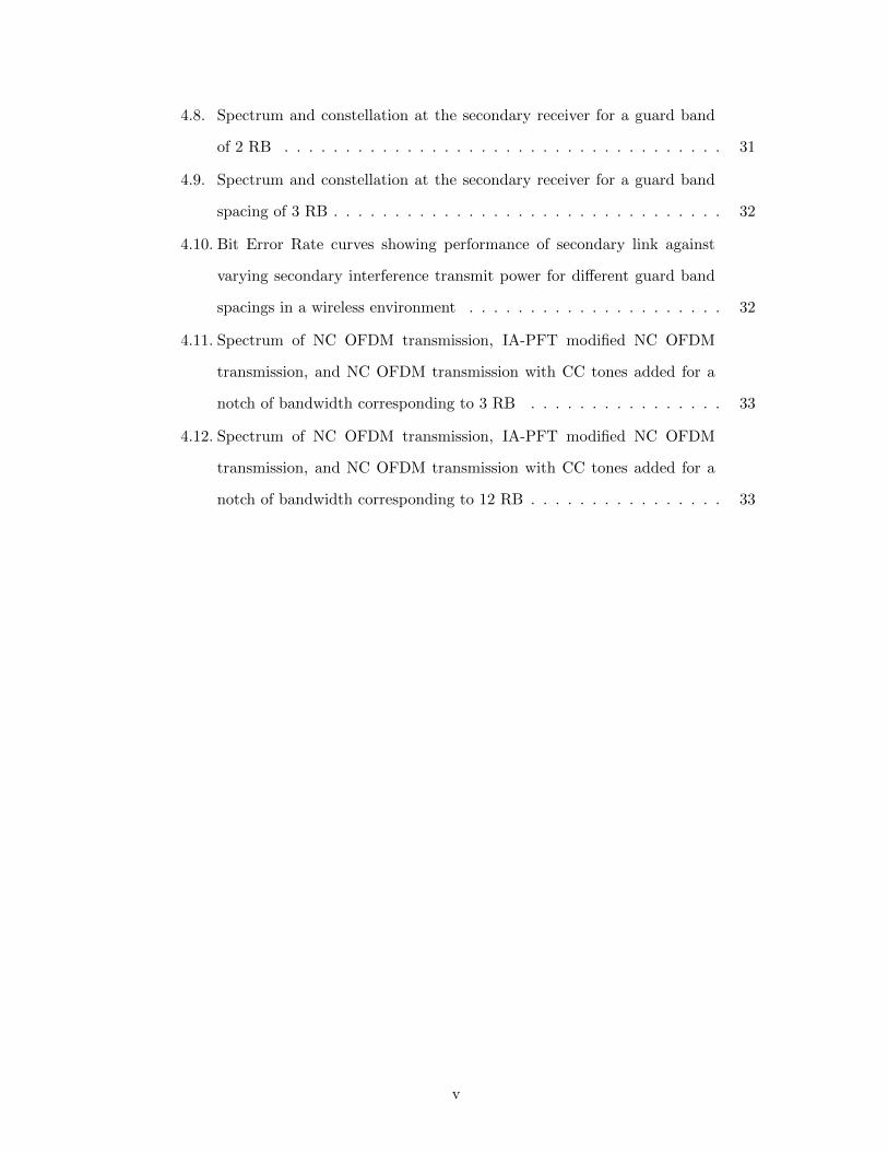
4.8. Spectrum and constellation at the secondary receiver for a guard band
of 2 RB . . . . . . . . . . . . . . . . . . . . . . . . . . . . . . . . . . . . 31
4.9. Spectrum and constellation at the secondary receiver for a guard band
spacing of 3 RB . . . . . . . . . . . . . . . . . . . . . . . . . . . . . . . . 32
4.10. Bit Error Rate curves showing performance of secondary link against
varying secondary interference transmit power for different guard band
spacings in a wireless environment . . . . . . . . . . . . . . . . . . . . . 32
4.11. Spectrum of NC OFDM transmission, IA-PFT modified NC OFDM
transmission, and NC OFDM transmission with CC tones added for a
notch of bandwidth corresponding to 3 RB . . . . . . . . . . . . . . . . 33
4.12. Spectrum of NC OFDM transmission, IA-PFT modified NC OFDM
transmission, and NC OFDM transmission with CC tones added for a
notch of bandwidth corresponding to 12 RB . . . . . . . . . . . . . . . . 33
v
Acknowledgements
I would like to thank firstly, my family and friends for their constant support throughout
the course of the project. I would like to express a special Thank You to Professor
Predrag Spasojevic, who was my thesis advisor. His invaluable guidance and advise
has helped me get through various stages of the project. The numerous discussions we
had on theory and implementation of communication systems has helped me learn a
lot. I would like to express my gratitude towards Professor David Daut and Professor
Zoran Gajic, who were members of the thesis commitee.
I would also like to thank my friends, faculty and staff at WINLAB and CORE,
Rutgers University. In particular, I would like to thank Abhishek Bindiganavile, Swap-
nil Mhaske, Samson Sequeira and Srinivas Pinagapany, who were a part of this research
project. I would also like to thank Mr John Scafidi ,who is the Systems Administrator
of the ECE Department without whose help, I could not have obtained access to needed
departmental facilities.
I would also like to thank Mr. Masayuki Ariyoshi and Mr. Yasunori Futatsugi of
System Platforms Research Labs, NEC Corporation, Japan for funding this research
project and their valuable support throughout the project. I would like to express my
gratitude to Mr. Ahsan Aziz, National Instruments, Austin, Texas, for his valuable
direction and help during numerous stages of the real time system design.
vi

Dedication
To my parents, teachers and friends
vii

Table of Contents
Abstract . . . . . . . . . . . . . . . . . . . . . . . . . . . . . . . . . . . . . . . . ii
List of Figures . . . . . . . . . . . . . . . . . . . . . . . . . . . . . . . . . . . . iv
Acknowledgements . . . . . . . . . . . . . . . . . . . . . . . . . . . . . . . . . vi
Dedication . . . . . . . . . . . . . . . . . . . . . . . . . . . . . . . . . . . . . . . vii
1. Introduction . . . . . . . . . . . . . . . . . . . . . . . . . . . . . . . . . . . 1
1.1. Background . . . . . . . . . . . . . . . . . . . . . . . . . . . . . . . . . . 1
1.2. Cognitive Radio Technology and Software Defined Radio . . . . . . . . . 2
1.3. Need for Secondary-to-Secondary Interference Evaluation . . . . . . . . 3
2. Coexistence of Heterogenous Secondary Links using DSA . . . . . . 4
2.1. Channel Model . . . . . . . . . . . . . . . . . . . . . . . . . . . . . . . . 4
2.2. Types of Dynamic Spectrum Access (DSA) techniques to achieve Secondary-
to-Secondary Coexistence . . . . . . . . . . . . . . . . . . . . . . . . . . 4
2.2.1. DSA using On/Off keying . . . . . . . . . . . . . . . . . . . . . . 5
2.2.2. DSA using secondary Non Contiguous OFDM transmission (NC-
OFDM) . . . . . . . . . . . . . . . . . . . . . . . . . . . . . . . . 5
2.2.3. DSA using IA-PFT modified NC-OFDM . . . . . . . . . . . . . . 6
2.3. IA-PFT theory . . . . . . . . . . . . . . . . . . . . . . . . . . . . . . . . 6
2.3.1. Carrier Cancellation by adding Active Interference Cancellation
tones to the NC OFDM transmission . . . . . . . . . . . . . . . . 7
2.3.2. Time Windowing using Raised Cosine filtering . . . . . . . . . . 10
3. Design and Implementation of the Secondary Transceiver System . 13
3.1. Real time system implementation concerns . . . . . . . . . . . . . . . . 13
viii
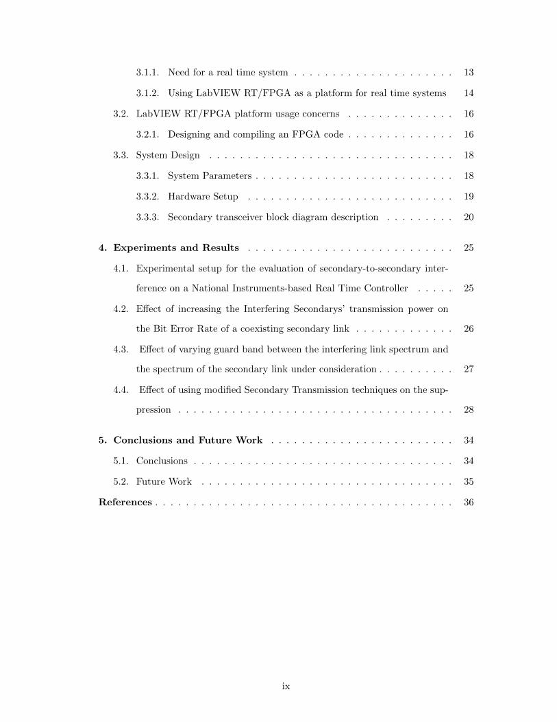
3.1.1. Need for a real time system . . . . . . . . . . . . . . . . . . . . . 13
3.1.2. Using LabVIEW RT/FPGA as a platform for real time systems 14
3.2. LabVIEW RT/FPGA platform usage concerns . . . . . . . . . . . . . . 16
3.2.1. Designing and compiling an FPGA code . . . . . . . . . . . . . . 16
3.3. System Design . . . . . . . . . . . . . . . . . . . . . . . . . . . . . . . . 18
3.3.1. System Parameters . . . . . . . . . . . . . . . . . . . . . . . . . . 18
3.3.2. Hardware Setup . . . . . . . . . . . . . . . . . . . . . . . . . . . 19
3.3.3. Secondary transceiver block diagram description . . . . . . . . . 20
4. Experiments and Results . . . . . . . . . . . . . . . . . . . . . . . . . . . 25
4.1. Experimental setup for the evaluation of secondary-to-secondary inter-
ference on a National Instruments-based Real Time Controller . . . . . 25
4.2. Effect of increasing the Interfering Secondarys’ transmission power on
the Bit Error Rate of a coexisting secondary link . . . . . . . . . . . . . 26
4.3. Effect of varying guard band between the interfering link spectrum and
the spectrum of the secondary link under consideration . . . . . . . . . . 27
4.4. Effect of using modified Secondary Transmission techniques on the sup-
pression . . . . . . . . . . . . . . . . . . . . . . . . . . . . . . . . . . . . 28
5. Conclusions and Future Work . . . . . . . . . . . . . . . . . . . . . . . . 34
5.1. Conclusions . . . . . . . . . . . . . . . . . . . . . . . . . . . . . . . . . . 34
5.2. Future Work . . . . . . . . . . . . . . . . . . . . . . . . . . . . . . . . . 35
References . . . . . . . . . . . . . . . . . . . . . . . . . . . . . . . . . . . . . . . 36
ix
1
Chapter 1
Introduction
1.1 Background
One of the major roadblocks in designing new wireless communication standards is the
issue of whether the current spectrum availability allows for the usage of transmission
specifications as desired by the standard. The available Radio Frequency (RF) spec-
trum is scarce and new emerging wireless technologies should try to achieve the best
performance under given bandwidth constraints. However, the allocated spectrum has
been heavily underutilized owing to current spectrum allocation policies. The Federal
Communications Commision(FCC) has recently released a set of frequency bands for
opportunistic access to ensure tighter control and to promote emerging wireless com-
munication standards. Dynamic Spectrum Access is one of the techniques to achieve
coexistence between two or more nodes sharing the same bandwidth. The FCC defines
two types of links that can use the same chunk of spectrum. The primary links are
licensed devices that are allocated the spectrum based on their needs and all the other
links will have to modify their transmission process to suit the bandwidth utilization
of the primary. The secondary link can be defined as any other unlicensed device that
can utilize the spectrum by opportunistic spectrum access and will have to modify its
transmission giving priority to the primary link.
Given that the primary has already been allocated its share of the spectrum, the
question arises as to how would the other secondary users utilize the remaining spec-
trum. The first issue is the fact that two or more secondary users may see the same
spectrum opportunity. This issue could be solved using advanced spectrum sensing
algorithms and designing protocols to avoid collision. The other major issue is that
of secondary links occupying adjacent frequency bins and interfering with each other.
2
This evaluation is important as it sheds light on parameters what need to be consid-
ered while designing secondary links. The aim of this thesis was to design a secondary
transceiver operating under LTE [1] specifications and evaluate secondary to secondary
coexistence. A part of this thesis also focuses on the implementation of a novel trans-
mission technique named Interference Avoidance by Partitioned Frequency- and Time-
domain processing( IA-PFT)[4] [6] which aims to further increase the performance of
the secondary links in consideration.
1.2 Cognitive Radio Technology and Software Defined Radio
Cognitive Radio can be termed as a paradigm for wireless communication in which
the network or the node itself modifies its transmission or reception parameters to
execute its tasks efficiently without causing hinderance to other users operating within
the same wireless environment. In other words, a Cognitive Radio System must possess
the capability to perform opportunistic access to enable coexistence of primary and
secondary users.
The most important part of Cognitive Radio Technology is the notion of a Soft-
ware Defined Radio [13]. A Software defined radio is a smart radio in which the var-
ious components of a radio which are typically implemented in hardware are instead
implemented by means of software on a Real Time Operating System or a Personal
Computer. Typical characteristics of an SDR are wideband RF converters, Digital-
to-Analog Converters (DAC), Analog-to-Digital Converters (ADC), multiband fron-
tend antennas and a general purpose processor, which handles the fundamental signal
processing. A Software Defined Radio (SDR) can be programmed to handle various
transmission and reception functionalities. Some of the transmission functionalities are
Adaptive Channel Modulation, changing the transmit power to adapt to the existing
environment, calculation of channel parameters,etc. A SDR can also perform various
receiver based functionalities like identification of channel modulation, error detection
and correction, spectrum sensing etc. A basic SDR may consist of a Real time Embed-
ded Controller with embedded FPGA modules , ADC /DAC and an RF daughter card.
In the experiments performed for the thesis, a similar setup has been used.
3
1.3 Need for Secondary-to-Secondary Interference Evaluation
In Dynamic Spectrum Access, the primary user has always been considered as the one
with the greatest priority and the secondary links modify their transmitted spectrum to
suit the primary user needs. However, the primary user occupies a very small part of the
available spectrum and the remaining portion has to be shared among secondary users.
Opportuinistic spectrum access can be realized by using both decentralized spectrum
allocation or using a central entity to monitor and control the sharing of the spectrum
among secondary users. The centralized control technique leads to more reliability and
ensures lesser secondary to secondary interference as secondary links are allocated the
spectrum based on what the central governing node sees. However, this technique is
more complicated as the entire allocation technique would break down if the central
governing unit fails to function. Also, the vacant frequency bins perceived by the central
governing technique may be different due to the fact that the central entity may not
detect the presence of a coexisting secondaries at respective frequency bins and regard
them as vacant. This is popularly known as the hidden node problem. The decentralized
spectrum allocation technique depends only upon what the relevant secondary users
percieve for spectrum allocation, and thus, will lead to better usage of vacant frequency
bins. Under this technique, multiple secondary networks may interfere with each other
if they see the same specrtrum opportunity. This kind of interference can be solved
using smart spectrum sensing and utilization techniques. Assuming that this problem
has been solved, there exists an issue of co-channel interference between secondary links
occupying adjacent frequency bins. Measurement of performance becomes important
in this case as the transmitting secondary will have to ensure that its transmission does
not affect the other secondary users operating in adjacent bands.
4
Chapter 2
Coexistence of Heterogenous Secondary Links using DSA
2.1 Channel Model
The channel model that has been assumed for the wireless environment is that of Ad-
ditive White Gaussian Noise (AWGN). According to the AWGN channel specifications,
the received signal y(t) can be expressed as an addition of the transmitted signal x(t)
and white Gaussian noise w(t). If we sample the received signal y(t) according to the
relation t=nT where n=0,1,....N-1, we can express y(n) as
y(n) = x(n) + w(n) (2.1)
2.2 Types of Dynamic Spectrum Access (DSA) techniques to achieve
Secondary-to-Secondary Coexistence
According to FCC regulations, the operator of an unlicensed RF device will need to
cease operation upon notification that the device is causing harmful interference. The
primary users have more priority than secondary users in spectrum access. This thesis
focuses on coexistence of secondary users assuming that the primary users have been
granted their requested share of the spectrum. The first step of DSA is spectrum
sensing to identify the positions of the vacant frequency bins. In this thesis, it has been
assumed that the positions are known, as the purpose of the thesis was to evaluate
performance and parameters for coexistence. Once spectrum sensing is performed,
the SDR has to modify the transmitted spectrum to suit the wireless environment.
Assuming that the underlying system is OFDM, there are many ways to modify the
secondary transmission. Some of the ways which are relevant to the thesis are explained
5
as follows.
2.2.1 DSA using On/Off keying
This type of secondary transmission is the most basic technique to enable primary
secondary coexistence. Whenever a primary signal is detected, the secondary OFDM
ceases to transmit. When there is no primary, it uses the complete band. However,
this method is not efficient as it does not employ efficient usage of available spectrum.
The main purpose of DSA is to solve the spectrum scarcity problem and this is not
completely addressed by this technique.
2.2.2 DSA using secondary Non Contiguous OFDM transmission (NC-
OFDM)
In this case, the secondary transmission is not stopped but modified when the primary
signal is detected. When there is no primary user active, the secondary transmission is
so modified to null out the secondary sub-carriers in the frequency bins that are occupied
by the primary transmission. This kind of modified OFDM transmission is called Non
Contiguous OFDM transmission (NC-OFDM). Non Contiguous OFDM transmission
operates in the following manner:
• Initially, the secondary receiver to scan the spectrum to detect presence of used
frequency bins. Various signal detection schemes can be used for this purpose,
the simplest being energy detection.
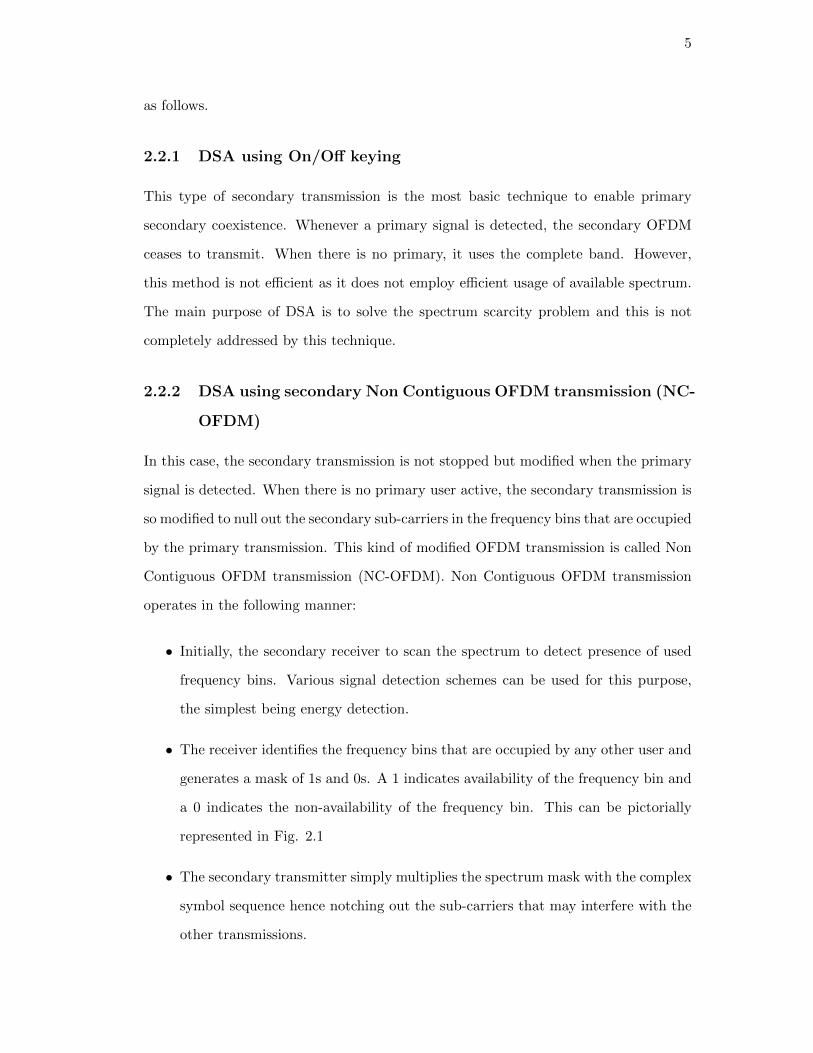
• The receiver identifies the frequency bins that are occupied by any other user and
generates a mask of 1s and 0s. A 1 indicates availability of the frequency bin and
a 0 indicates the non-availability of the frequency bin. This can be pictorially
represented in Fig. 2.1
• The secondary transmitter simply multiplies the spectrum mask with the complex
symbol sequence hence notching out the sub-carriers that may interfere with the
other transmissions.
6
Figure 2.1: Spectrum mask calculated based on availability of frequency bins [7]
The pitfall of this method is that even though the sub-carriers are being notched out
at the appropriate locations, there is spectral leakage from the sub-carriers adjacent due
to the notch. Thus, the suppression gain is not adequate and it may lead to interference
with the secondary user occupying those particular frequency bins.
2.2.3 DSA using IA-PFT modified NC-OFDM
As discussed before, the suppression gain at the notch is not adequate for regular NC-
OFDM. Interference Avoidance by Partitioned Frequency and Time-domain Processing
is a novel technique to increase the suppression within the null band with respect to
a particular Secondary NC OFDM transceiver. It employs various signal processing
algorithms in the time and frequency domain to help achieve more suppression in the
null band. The IA-PFT theory has been explained further in section 2.3 of the thesis.
2.3 IA-PFT theory
As discussed before, due to poor filter characteristics of the baseband transceiver and
due to spectral leakage from adjacent sub-carriers with respect to the notch, the sup-
pression gain within the notch is not adequate. This may lead to reduction in the
performance of the secondary link occupying adjacent resource blocks for transmission.
IA-PFT is a novel technique proposed by NEC-Laboratories, Japan [6] that basically
modifies the Non Contiguous OFDM symbol both in the Time and the Frequency do-
main to achieve further suppression gain. It is composed of two parallel operations

7
namely Time Windowing and Carrier Cancellation. As the name suggests, Time Win-
dowing is performed on the OFDM samples in the time domain after the IFFT block
in the OFDM sequence of operations whereas Carrier Cancellation is performed after
the sub-carrier mapping before the IFFT block. A detailed description of both these
techniques is as follows.
2.3.1 Carrier Cancellation by adding Active Interference Cancellation
tones to the NC OFDM transmission
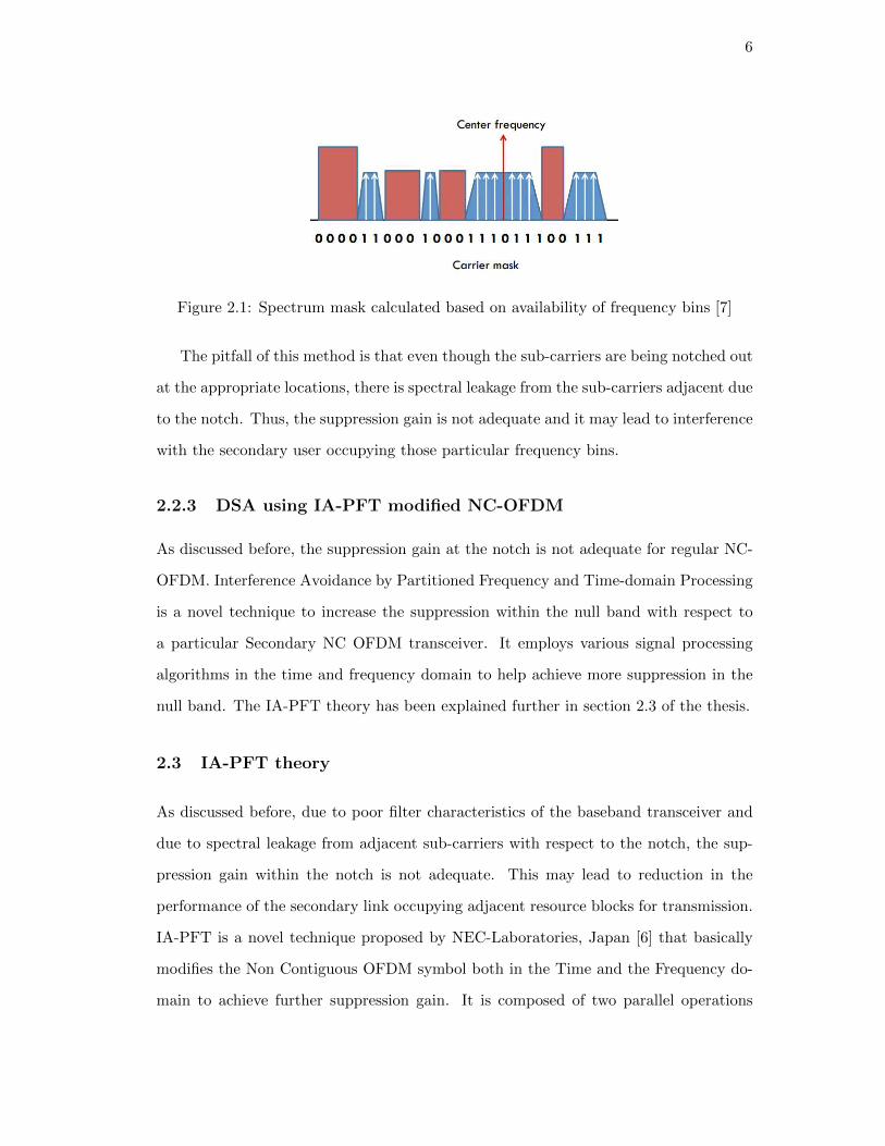
Active Interference Cancellation (AIC)[5] [7] [8] is a technique that proposes to add two
or more extra sub-carriers besides the existing sub-carriers that lie in the user band.
The purpose of adding these tones is to cancel out the interference due to sidelobes
of the existing sub-carriers. Assuming the secondary link has estimated the unused
frequency bins and determined the positions of the sub-carriers that have to be nulled,
the spectrum can be pictorially represented in Fig. 2.2. As indicated in the figure,
spectrum can be divided into two complementary parts. The part of the spectrum that
has been utilized by the secondary to transmit data can be labelled as the Information
band whereas the part of the spectrum which may contain sub-carriers that arise due
to the sidelobe interference of the information bearing - of the secondary link can be
labelled as the Interference band. AIC removes one or more of these additional tones
and replaces them with a new set of tones called AIC tones that effectively aid in nulling
out the sidelobe interference caused by the information bearing sub-carriers.
The first step of the AIC technique is to compute the sidelobe interference in the
Interference band. AIC computes the sidelobe interference in the interference band by
turning off the interference tones and replacing them with AIC tones. The complex
symbol sequence X is upsampled in the frequency domain by a factor of M.
Suppose X(k) where k=0,....,N-1, represents the original frequency domain data
symbols where N is the FFT size. The time domain data signal is as follows
x(n) =N−1∑k=0
X(k)exp(j2πnk
N) (2.2)
8
Figure 2.2: Spectrum showing positions of Interference and AIC tones
If the corresponding spectrum is upsampled by a factor of M, the new upsampled
sequence Y is given by
Y(l) =1
N
N−1∑n=0
x(n)exp(−j2π nl
NM) (2.3)
Using the above equations , the following relationships can be determined
Y(l) =1
N
N−1∑k=0
N−1∑n=0
X(k)exp(−j2π nN
(k − l
M)) (2.4)
Or
Y =1
NPX (2.5)
Where
X = [X(0)....X(N)]′ (2.6)
P represents the upsampling matrix which when multiplied with any complex se-
quence, the upsampled version of the respective complex sequence would be generated.
P(l, k) =N−1∑n=0
exp(−j2π nN
(k − l
M)) (2.7)
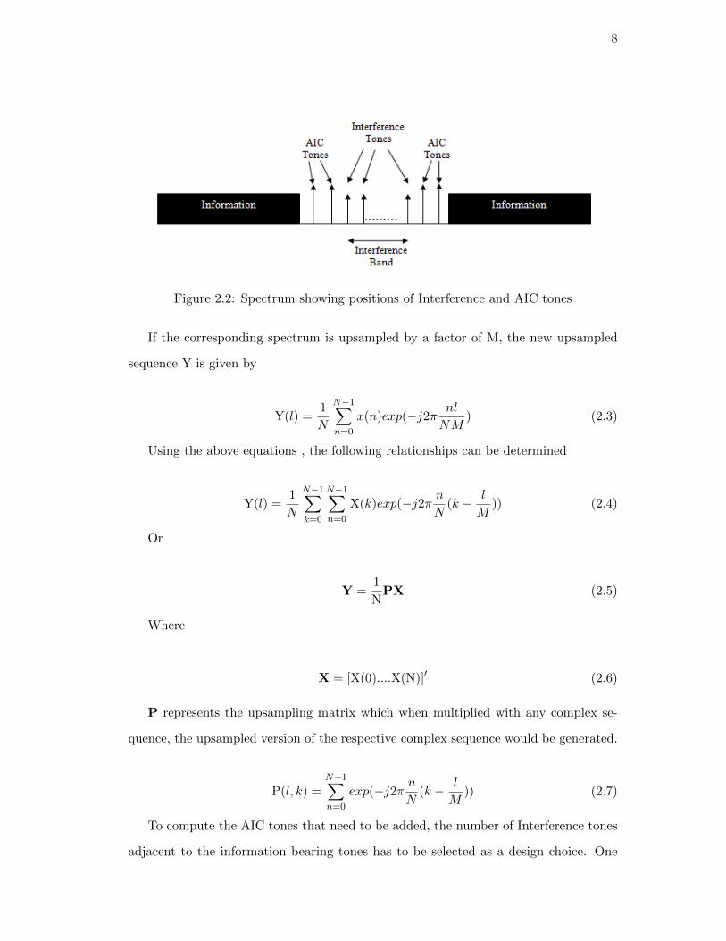
To compute the AIC tones that need to be added, the number of Interference tones
adjacent to the information bearing tones has to be selected as a design choice. One
9
can assume that the interference tones nearest to the information bearing sub-carriers
will have more sidelobe interference but this may not be entirely true. Suppose the
Interference tones considered start from (p)th to (p + Ni − 1)th sub-carrier. where Ni
stands for the number of interference tones considered. We can define a nulling matrix
T of size N by N. The matrix T is a sparse diagonal matrix and its diagonal elements
contain zeros at all the positions except at the positions of the information bearing
sub-carriers where they are ones. The interference generated by these sub-carriers can
be computed as
dl = PsTX (2.8)
Where Ps is a submatrix of P by taking its row corresponding to the upsampled
spectrum in the interference band i.e from M(p+1)th to M(p+Ni-1)th rows of P. The
new set of sub-carriers say h that need to be placed to cancel out the interference due
to dl can be computed as
Pnh = −dl (2.9)
Pn is a submatrix of Ps corresponding to the Interference tones and the AIC tones.
The size of Pn is (M(Ni-1)+1) by (Ni+2). Finally to compute h we can formulate a
least squares expression. Since Pn is not a square matrix one can use the pseudoinverse
equation to compute h as
h = −(P′nPn)−1P′ndl (2.10)
Addition of these AIC tones has to be performed for the either ends of the Interfer-
ence bands. AIC tone insertion leads to cancellation of interference at the sides of the
Interference bands and thus leads to suppression gain. This technique is performed at
the sub-carrier level and thus has to be added before performing IFFT in the OFDM
sequence of operations.

10
Figure 2.3: Steps to illustrate Time Windowing process [7] [8]
2.3.2 Time Windowing using Raised Cosine filtering
Time Windowing performs raised cosine filtering of the OFDM samples after the IFFT
block. Typically LTE [1] or any other communication standard recommends addition
of cyclic prefix to OFDM symbol for a variety of reasons like eliminating Intersymbol
Interference, Symbol Synchronization, etc. In addition to the cyclic prefix, Time Win-
dowing specifies addition of another set of samples at the end of the OFDM symbol.
These samples are termed as overlap and they are generally equal to the first few sam-
ples of the original OFDM symbol excluding the cyclic prefix.Thus, the modified OFDM
symbol contains the cyclic prefix attached to the front and the overlap attached at the
end. The size of the overlap is a design criterion and can be varied depending upon the
required suppression gain. The first few samples corresponding to the overlap size of
the modified OFDM symbol are raised cosine filtered with a positive ramp and the last
few samples are raised cosine filtered with a negative ramp. The samples corresponding
to the overlap portion of the modified OFDM symbol are added to the first few samples
of the succeeding OFDM symbol and the overlap is discarded. In essence, the modified
OFDM symbol on which time windowing is performed is similar to the original OFDM
symbol with exception of the first few samples of the cyclic prefix which have been
modified. Thus there is an interdependence of every OFDM symbol with the preceding
OFDM symbol. Figure 2.3 illustrates the Time Windowing process.
11
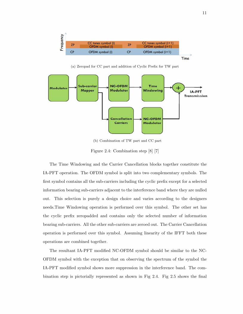
(a) Zeropad for CC part and addition of Cyclic Prefix for TW part
(b) Combination of TW part and CC part
Figure 2.4: Combination step [8] [7]
The Time Windowing and the Carrier Cancellation blocks together constitute the
IA-PFT operation. The OFDM symbol is split into two complementary symbols. The
first symbol contains all the sub-carriers including the cyclic prefix except for a selected
information bearing sub-carriers adjacent to the interference band where they are nulled
out. This selection is purely a design choice and varies according to the designers
needs.Time Windowing operation is performed over this symbol. The other set has
the cyclic prefix zeropadded and contains only the selected number of information
bearing sub-carriers. All the other sub-carriers are zeroed out. The Carrier Cancellation
operation is performed over this symbol. Assuming linearity of the IFFT both these
operations are combined together.
The resultant IA-PFT modified NC-OFDM symbol should be similar to the NC-
OFDM symbol with the exception that on observing the spectrum of the symbol the
IA-PFT modified symbol shows more suppression in the interference band. The com-
bination step is pictorially represented as shown in Fig 2.4. Fig 2.5 shows the final
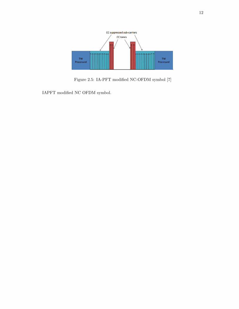
12
Figure 2.5: IA-PFT modified NC-OFDM symbol [7]
IAPFT modified NC OFDM symbol.
13
Chapter 3
Design and Implementation of the Secondary Transceiver
System
3.1 Real time system implementation concerns
3.1.1 Need for a real time system
A real time system can be defined as a system which guarantees response within strict
time constraints. It is generally a misconception that real time systems should neces-
sarily have a fast response time. That is not entirely true. A non real time system may
be fast but does not guarantee a fixed response time when it is triggered. Some of the
attributes of a real time system are as follows:
• Loop Cycle time: Loop Cycle time is defined as the execution time of a block
within a single loop.
• Jitter: The jitter in the system characterizes the variation in the execution time
as opposed to the desired response time.
• Priority: If a real time system is given many tasks, priority defines the importance
of a particular task in relation to the other tasks.
Thus a real time system must have the notion of a fixed response time with less
jitter and defined priority. The aim of this thesis is to evaluate secondary-to-secondary
interference in an LTE-esque environment. LTE specifications demand both stringent
timing considerations and operation within a defined Bandwidth. So, to ensure that
experiments are performed with LTE specifications taken into consideration, a real time
system implementation becomes essential.

14
3.1.2 Using LabVIEW RT/FPGA as a platform for real time systems
National Instruments-based LabVIEW RT/FPGA [9] [12] was chosen to be the platform
for the implementation of a LTE-esque communication system. The choice of LabVIEW
was based on its efficiency and simplicity of use. LabVIEW provides a graphical en-
vironment and has an extensive Math, DSP and RF Communications libraries which
enable easier transition from design to implementation. LabVIEW provides a stable
real time environment for communication systems development. Certain important
features required by the RT system are satisfied by various features of the LabVIEW
development environment. For highly time constrained operations the FPGA environ-
ment can also be used. LabVIEW FPGA environment provides for higher clock rates
and can be programmed to run time sensitive tasks. FPGA programming in LabVIEW
is easier since it does not involve the need for VHDL/Verilog programming. Using a
block diagram approach, LabVIEW provides a higher level of abstraction, and hence,
FPGA coding becomes relatively less complicated. LabVIEW provides certain inter-
esting and important tools relevant to a real time System. Some of these tools are
described as follows:
• Timed Loop
As explained before Timing is a very important consideration in a real time sys-
tem. In any real time system, various tasks have to be executed repeatedly
according to specified time considerations. The allocation of resources and pro-
cessor cycles to each of these operations becomes important. Timed loops take
care of the timing and priority of each of these tasks. Timed loop can be defined
as a structure that ensures that the sequence of functional blocks within itself is
executed at a specified rate. A timed loop is as shown in Fig.3.1. Each timed loop
has various controls and indicators. Using a faster or slower clock, one can change
the execution time to suit the requirements of the system design. One can also
set the priority level of a particular timed loop depending on importance of the
operation. Timing errors are also indicated using Boolean logic indicators which
further help in debugging. In the figure, the execution time is specified to be 1

15
Figure 3.1: Timed loop in LabVIEW
ms. So if the execution time exceeds the specified limit, the Timed Out Indicator
glows enabling the user to consider restructuring the code for faster execution.
• DMA
DMA stands for Direct Memory Access. In any FPGA-based code, queuing
becomes a very important component of the design. In order to transfer high
amounts of data at high rates between the target and the host as would be the
case of a communication system, the best way to buffer data is to use DMA.
DMA in LabVIEW can be implemented using FIFOs( First in First out) [12].
The use of a FIFO is to buffer samples generated by a previous block and release
samples required by the second block, as and when, the succeeding block is ready.
For instance, assuming that the first block operates at 20 MSamples/sec and the
succeeding block operates at a lower rate say 10 Msamples/sec. If the two blocks
were wired together directly without using FIFOs, the second it would lead into a
sample overflow problem as the second block will not be able to keep up with the
operation of the first block. However, if a FIFO is used between the two blocks
, the FIFO will be able to buffer samples at a higher rate and release samples as
and when the second block is ready to process them and this will ensure a sys-
tematic flow of samples between the two blocks. FIFOs are thus used to interface
between two blocks operating at different rates. The depth of the FIFO defines

16
Figure 3.2: A typical FIFO method node in LabVIEW
the number of elements that the FIFO can buffer. Depending upon the difference
in the rate of operation between the two blocks, the depth of the FIFO can be set.
The timed out indicator enables the user to identify if the FIFO times out if an
output request is sent. The FIFO parameters are set using FIFO method nodes
in LabVIEW. A FIFO can be programmed to be storing samples or transmitting
them depending upon the need of the task. One can also monitor the status of
a FIFO using the specified method node. Figure 3.2 shows a FIFO method node
in LabVIEW.
• Shared Variable
LabVIEW provides a shared variable structure which enables sharing of data
between the host and the target and between various sub operations within the
same host/target. These structures become very important in case of operations
like Bit Error Rate measurements that can be performed at the host by processing
samples obtained from various blocks mapped to the target.
3.2 LabVIEW RT/FPGA platform usage concerns
3.2.1 Designing and compiling an FPGA code
FPGA code design in LabVIEW follows a higher level of abstraction and thus, is rel-
atively easier to design the flow of logic as compared to VHDL/Verilog based coding.
The LabVIEW FPGA module coding is slightly different than the normal host based
coding and will prove to be efficient if particular incremental steps are followed to code.
The design flow that has been found to be more efficient is shown in Fig. 3.3.
The first step towards coding any FPGA based code is the defining the architecture
of the code i.e. defining its functionality, inputs, outputs, etc. Once that is mapped
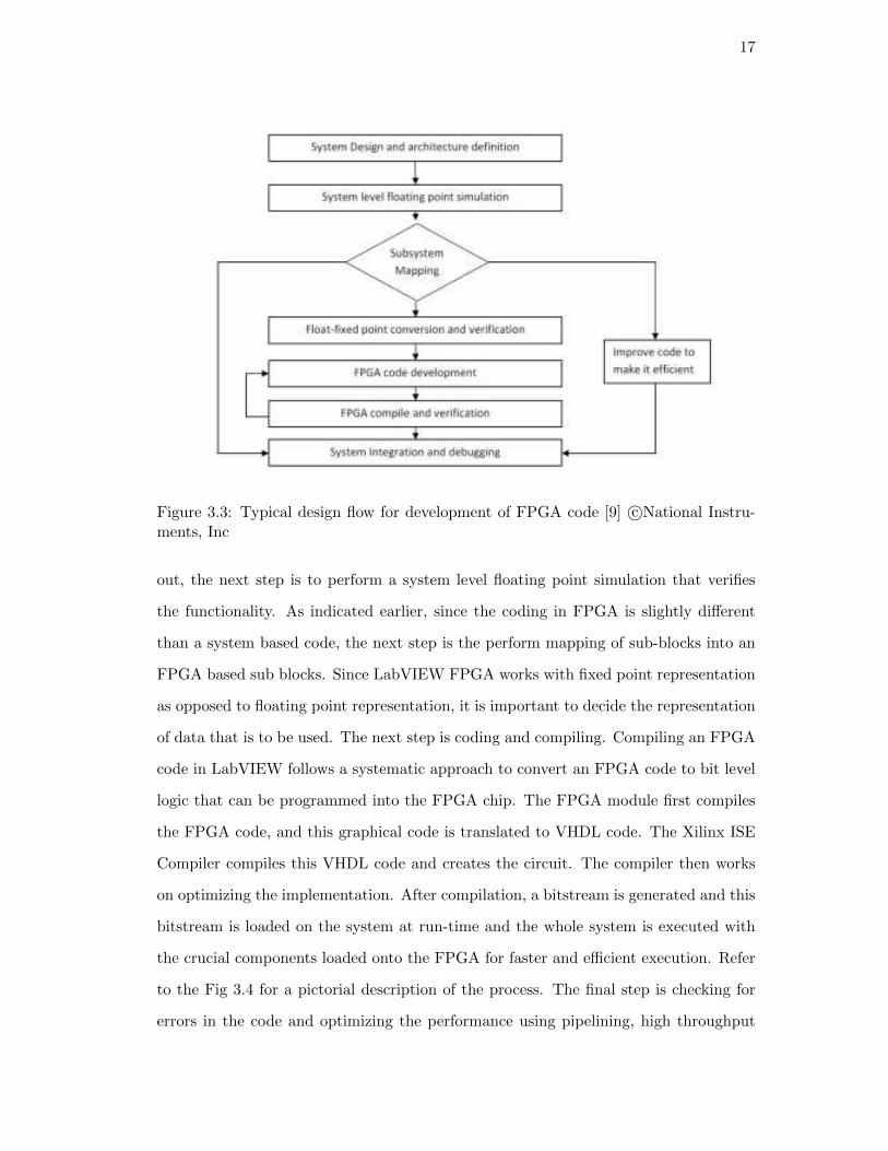
17
Figure 3.3: Typical design flow for development of FPGA code [9] c©National Instru-ments, Inc
out, the next step is to perform a system level floating point simulation that verifies
the functionality. As indicated earlier, since the coding in FPGA is slightly different
than a system based code, the next step is the perform mapping of sub-blocks into an
FPGA based sub blocks. Since LabVIEW FPGA works with fixed point representation
as opposed to floating point representation, it is important to decide the representation
of data that is to be used. The next step is coding and compiling. Compiling an FPGA
code in LabVIEW follows a systematic approach to convert an FPGA code to bit level
logic that can be programmed into the FPGA chip. The FPGA module first compiles
the FPGA code, and this graphical code is translated to VHDL code. The Xilinx ISE
Compiler compiles this VHDL code and creates the circuit. The compiler then works
on optimizing the implementation. After compilation, a bitstream is generated and this
bitstream is loaded on the system at run-time and the whole system is executed with
the crucial components loaded onto the FPGA for faster and efficient execution. Refer
to the Fig 3.4 for a pictorial description of the process. The final step is checking for
errors in the code and optimizing the performance using pipelining, high throughput

18
Figure 3.4: FPGA compile server [9] c©National Instruments, Inc
block usage, etc.
3.3 System Design
3.3.1 System Parameters
The aim of this thesis was to evaluate secondary-to-secondary coordination and coex-
istence. To serve this purpose more effectively, the realization of an LTE-esque com-
munications system was crucial. A LTE based secondary NC-OFDM transceiver was
designed and implemented for this purpose. From the LTE standard specifications,
the underlying system is OFDM. Fig 3.5 shows some of the LTE specifications. The
secondary transceiver design specifications that have been implemented for the system
are as follows:
• Bandwidth: 20 MHz
• SubFrame duration: 1 ms
• No. of Sub-carriers: 1200
• Sub-carrier spacing: 15kHz
• Sub-carrier Mapping : Quadrature Phase Shift Keying (QPSK)
• Use of 1 Reference Carrier every 5 data carriers for equalization and channel
estimation

19
Figure 3.5: LTE specifications [1]
3.3.2 Hardware Setup
It is important to discuss the Hardware Setup before discussion of the transceiver design
as most of the design choices depend upon the Hardware Setup. The setup consists of
a Windows based Host machine containing the LabVIEW user interface. The real time
machine is a National Instruments-based PXIe-8133 Real Time Controller with support
for LabVIEW Real Time Module (LabVIEW RT). The LabVIEW system code is built
on the Host machine and is ported on to the RT controller using Ethernet. The RT
controller has two Xilinx Virtex-5 based FPGA chips interfaced to itself. The FPGA
chips can be programmed using LabVIEW FPGA module which can be controlled using
the Host interface. Each FPGA chip streams data to an NI-based Baseband Transceiver
kit. The Baseband Transceiver module contains two 16 bit DACs and 14 bit ADCs
operating at a sampling rate of 100 MSamples/sec for both I and Q components (50
Complex MSamples/sec overall). The Baseband transceiver talks to the RF daughter
board via an NI-based Interposer. The RF daughter board is the Ettus XCVR 2450
which operates at center frequency of 2.45-2.49/4.9-5 GHz and is capable of a maximum
transmit power of 20 dBM. The hardware setup for experiments conducted in this study
is shown in Fig 3.6.
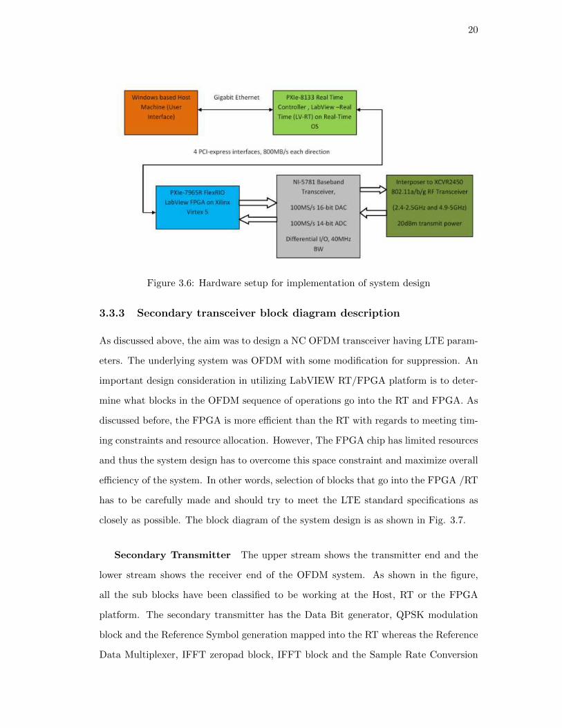
20
Figure 3.6: Hardware setup for implementation of system design
3.3.3 Secondary transceiver block diagram description
As discussed above, the aim was to design a NC OFDM transceiver having LTE param-
eters. The underlying system was OFDM with some modification for suppression. An
important design consideration in utilizing LabVIEW RT/FPGA platform is to deter-
mine what blocks in the OFDM sequence of operations go into the RT and FPGA. As
discussed before, the FPGA is more efficient than the RT with regards to meeting tim-
ing constraints and resource allocation. However, The FPGA chip has limited resources
and thus the system design has to overcome this space constraint and maximize overall
efficiency of the system. In other words, selection of blocks that go into the FPGA /RT
has to be carefully made and should try to meet the LTE standard specifications as
closely as possible. The block diagram of the system design is as shown in Fig. 3.7.
Secondary Transmitter The upper stream shows the transmitter end and the
lower stream shows the receiver end of the OFDM system. As shown in the figure,
all the sub blocks have been classified to be working at the Host, RT or the FPGA
platform. The secondary transmitter has the Data Bit generator, QPSK modulation
block and the Reference Symbol generation mapped into the RT whereas the Reference
Data Multiplexer, IFFT zeropad block, IFFT block and the Sample Rate Conversion
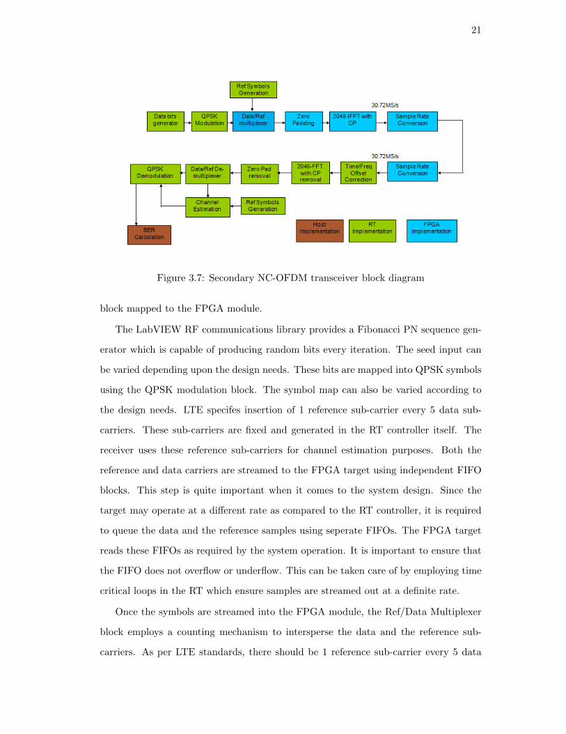
21
Figure 3.7: Secondary NC-OFDM transceiver block diagram
block mapped to the FPGA module.
The LabVIEW RF communications library provides a Fibonacci PN sequence gen-
erator which is capable of producing random bits every iteration. The seed input can
be varied depending upon the design needs. These bits are mapped into QPSK symbols
using the QPSK modulation block. The symbol map can also be varied according to
the design needs. LTE specifes insertion of 1 reference sub-carrier every 5 data sub-
carriers. These sub-carriers are fixed and generated in the RT controller itself. The
receiver uses these reference sub-carriers for channel estimation purposes. Both the
reference and data carriers are streamed to the FPGA target using independent FIFO
blocks. This step is quite important when it comes to the system design. Since the
target may operate at a different rate as compared to the RT controller, it is required
to queue the data and the reference samples using seperate FIFOs. The FPGA target
reads these FIFOs as required by the system operation. It is important to ensure that
the FIFO does not overflow or underflow. This can be taken care of by employing time
critical loops in the RT which ensure samples are streamed out at a definite rate.
Once the symbols are streamed into the FPGA module, the Ref/Data Multiplexer
block employs a counting mechanism to intersperse the data and the reference sub-
carriers. As per LTE standards, there should be 1 reference sub-carrier every 5 data
22
sub-carriers. For every OFDM symbol, LTE specifies 1000 data sub-carriers and 200
reference sub-carriers for a bandwidth of 20 MHz. Once these sub-carriers are inter-
leaved, we get 1200 sub-carriers per OFDM symbol. Since an IFFT of size 2048 is
used, these 1200 symbols must be zeropadded on either side. This is performed by the
Zeropadding block. The design uses the Xilinx IP( Intellectual Property) to realize the
IFFT module. This is done to ensure efficiency and robustness. It also inserts a cyclic
prefix of length 512 sub-carriers to ensure lesser Inter Symbol Interference and also for
OFDM symbol synchronization. The baseband transceiver (ADC/DAC) in the hard-
ware setup works at 50 complex Msamples/sec. However, the sampling rate obtained
by the system at the end of the IFFT block is 30.72 complex MSamples/sec. If this is
directly fed to the DAC, it will lead to undersampling of the DAC and the DAC will
tend to insert garbage samples to overcome the rate difference. Thus, resampling is
required. This is done using the sample rate conversion blocks which upsamples the
output of the IFFT to ensure a rate of 50 complex MSamples/sec.
FPGA module design for NC OFDM transmitter We have discussed the
design for a basic OFDM transmitter. The NC OFDM transmitter design is relatively
straightforward and just involves nulling out the sub-carriers at the positions of used
frequency bins. In our experiments, it has been assumed that the positions of the
vacant frequency bins are previously known to the Secondary transceiver and thus the
only changes in the design relative to the OFDM transmitter would be zeroing out the
sub-carriers occupying used frequency bins of the spectrum in the QPSK modulation
and reference symbols generation blocks in the OFDM transmitter.
Design of IA-PFT-based NC OFDM transmitter IAPFT involves two ma-
jor operations - Carrier Cancellation and Time Windowing. The Time Windowing is
performed at after the IFFT block, and hence, requires modifications in the FPGA
module. The insertion of AIC tones of the Carrier Cancellation operation have to be
done at the RT controller owing to the design choice since the Reference and the Data
Symbols generation is performed at the RT end. However, for the IA-PFT design, the
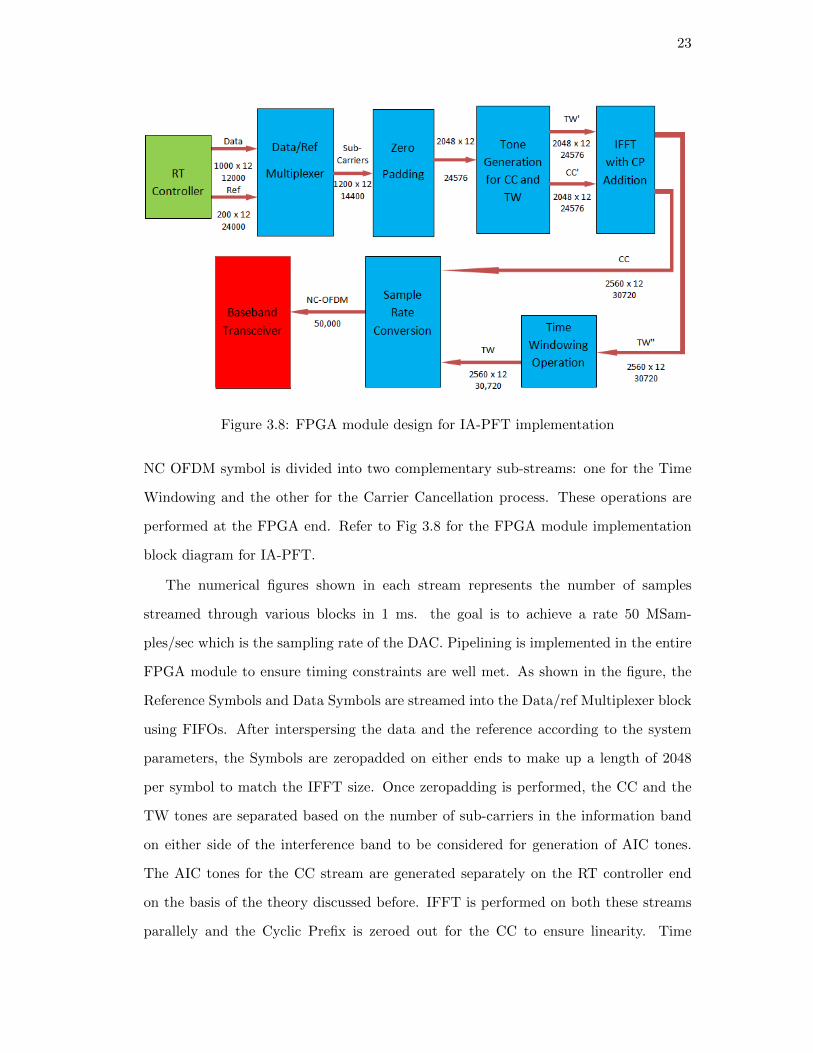
23
Figure 3.8: FPGA module design for IA-PFT implementation
NC OFDM symbol is divided into two complementary sub-streams: one for the Time
Windowing and the other for the Carrier Cancellation process. These operations are
performed at the FPGA end. Refer to Fig 3.8 for the FPGA module implementation
block diagram for IA-PFT.
The numerical figures shown in each stream represents the number of samples
streamed through various blocks in 1 ms. the goal is to achieve a rate 50 MSam-
ples/sec which is the sampling rate of the DAC. Pipelining is implemented in the entire
FPGA module to ensure timing constraints are well met. As shown in the figure, the
Reference Symbols and Data Symbols are streamed into the Data/ref Multiplexer block
using FIFOs. After interspersing the data and the reference according to the system
parameters, the Symbols are zeropadded on either ends to make up a length of 2048
per symbol to match the IFFT size. Once zeropadding is performed, the CC and the
TW tones are separated based on the number of sub-carriers in the information band
on either side of the interference band to be considered for generation of AIC tones.
The AIC tones for the CC stream are generated separately on the RT controller end
on the basis of the theory discussed before. IFFT is performed on both these streams
parallely and the Cyclic Prefix is zeroed out for the CC to ensure linearity. Time
24
Windowing using raised cosine filtering is performed on the TW stream. The CC and
the TW sets are streamed out at a rate 30,720 Msamples/sec after this stage. These
streams are added together at the Sample Rate Conversion block and upsampled to a
rate of 50 complex Msamples/sec (100 Msamples/sec for both I and Q), the rate which
is required by the baseband transceiver. These describe the modifications that need
to be made to the existing NC OFDM transmission for building an IA-PFT based NC
OFDM transmission.
Secondary Receiver The receiver design has been completely mapped on the
RT controller with the exception of the sample rate conversion block owing to ease of
design. The samples are acquired at the RF end by the XCVR daughter board, and
transfers received I/Q samples to the ADC on the NI-5781 Baseband Transceiver, which
converts this RF signal into baseband spectrum. These samples are downsampled at
the FPGA end using a resampler to regain the rate of 30,720 Msamples/sec. A FIFO
is used to queue these samples which wait on processing by the RT controller. To
perform Time/Frequency Offset estimation, the design uses the Maximum-Likelihood
Estimnation technique described by [11]. Once each OFDM symbol is isolated by this
method, the Cyclic Prefix is removed and an 2048 pt FFT is performed to recover
the sub-carriers. The sub-carriers recovered are composed of both data and reference
symbols interspersed with each other. A demultiplexing operation is performed to
isolate the data and the reference symbols. The reference symbols are used for channel
estimation. The channel estimation block uses the least squares estimation technique
described by [11] to obtain channel coefficients . These channel coefficients are used to
estimate the original data symbol set that had been transmitted. The data carriers so
obtained are QPSK symbols following a Gray Coding scheme. Using the sign of each
symbol, bits are recovered at the receiver end. The BER calculations are performed
over the recovered bits for error performance measurement.
25
Chapter 4
Experiments and Results
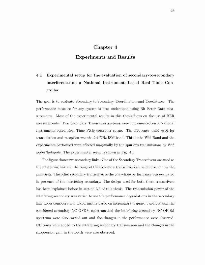
4.1 Experimental setup for the evaluation of secondary-to-secondary
interference on a National Instruments-based Real Time Con-
troller
The goal is to evaluate Secondary-to-Secondary Coordination and Coexistence. The
performance measure for any system is best understood using Bit Error Rate mea-
surements. Most of the experimental results in this thesis focus on the use of BER
measurements. Two Secondary Transceiver systems were implemented on a National
Instruments-based Real Time PXIe controller setup. The frequency band used for
transmission and reception was the 2.4 GHz ISM band. This is the Wifi Band and the
experiments performed were affected marginally by the spurious transmissions by Wifi
nodes/hotspots. The experimental setup is shown in Fig. 4.1
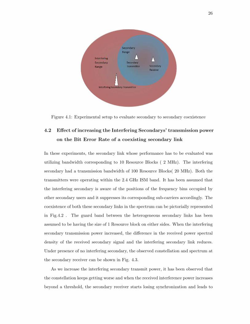
The figure shows two secondary links. One of the Secondary Transceivers was used as
the interfering link and the range of the secondary transceiver can be represented by the
pink area. The other secondary transceiver is the one whose performance was evaluated
in presence of the interfering secondary. The design used for both these transceivers
has been explained before in section 3.3 of this thesis. The transmission power of the
interfering secondary was varied to see the performance degradations in the secondary
link under consideration. Experiments based on increasing the guard band between the
considered secondary NC OFDM spectrum and the interfering secondary NC-OFDM
spectrum were also carried out and the changes in the performance were observed.
CC tones were added to the interfering secondary transmission and the changes in the
suppression gain in the notch were also observed.
26
Figure 4.1: Experimental setup to evaluate secondary to secondary coexistence
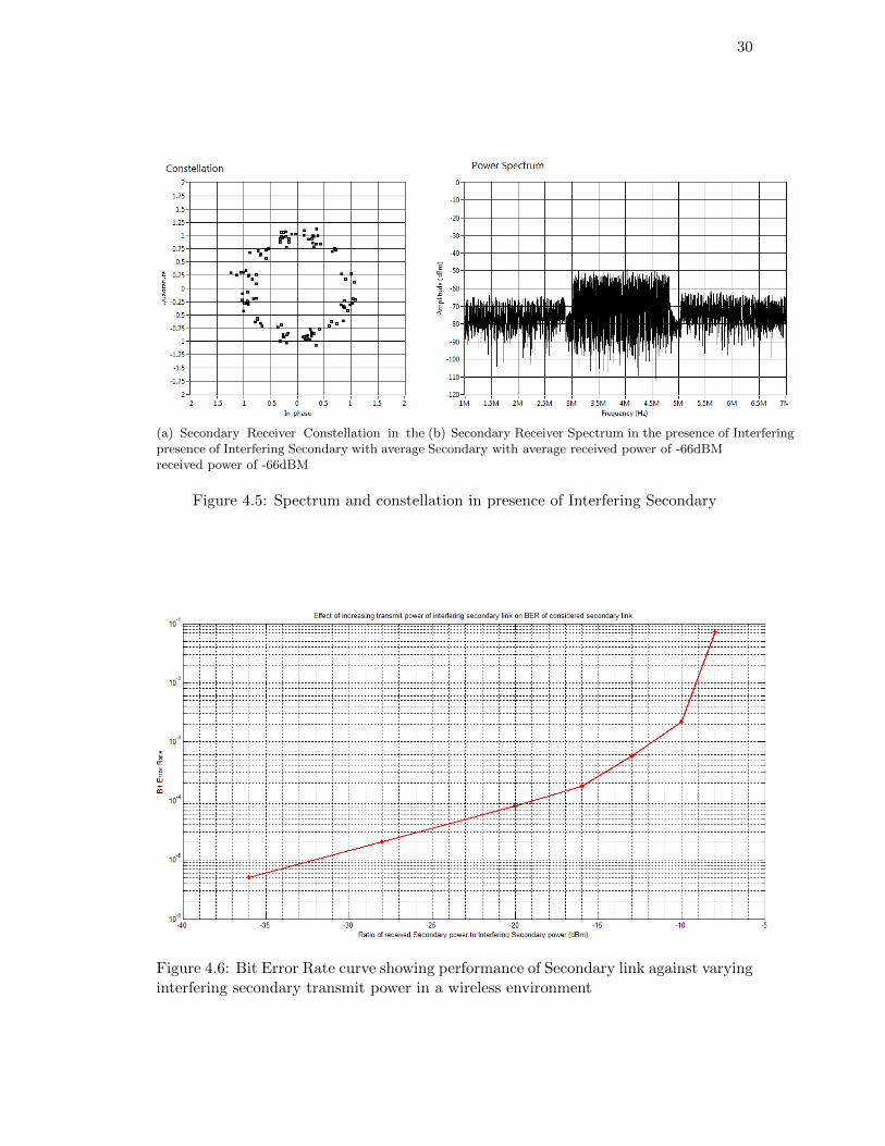
4.2 Effect of increasing the Interfering Secondarys’ transmission power
on the Bit Error Rate of a coexisting secondary link
In these experiments, the secondary link whose performance has to be evaluated was
utilizing bandwidth corresponding to 10 Resource Blocks ( 2 MHz). The interfering
secondary had a transmission bandwidth of 100 Resource Blocks( 20 MHz). Both the
transmitters were operating within the 2.4 GHz ISM band. It has been assumed that
the interfering secondary is aware of the positions of the frequency bins occupied by
other secondary users and it suppresses its corresponding sub-carriers accordingly. The
coexistence of both these secondary links in the spectrum can be pictorially represented
in Fig.4.2 . The guard band between the heterogeneous secondary links has been
assumed to be having the size of 1 Resource block on either sides. When the interfering
secondary transmission power increased, the difference in the received power spectral
density of the received secondary signal and the interfering secondary link reduces.
Under presence of no interfering secondary, the observed constellation and spectrum at
the secondary receiver can be shown in Fig. 4.3.
As we increase the interfering secondary transmit power, it has been observed that
the constellation keeps getting worse and when the received interference power increases
beyond a threshold, the secondary receiver starts losing synchronization and leads to

27
a poorer performance. The spectra and the constellation plots observed on increasing
the interfering transmission have been shown in Fig 4.5. To quantify these effects a
performance measurement of the Secondary link in terms of Bit Error Rate became
necessary. The received SNR of the secondary link in consideration was kept constant
and the transmit power of the Interfering Secondary was varied. The Bit Error Rate
curve for the secondary link is as shown in figure. In order to obtain an optimal range
of BER values, a total of 396,000 bits were used for calcluation. It is observed that
as the interfering link power is increased, the BER increases. The BER curve for the
secondary link is as shown in Fig. 4.6.
4.3 Effect of varying guard band between the interfering link spec-
trum and the spectrum of the secondary link under consideration
To evaluate coexistence of secondary links, it is important to draw out certain trans-
mission parameters. The guard band that needs to be maintained between the spectra
of secondary links is an important parameter that needs to be measured to ensure
proper coexistence. Experiments were performed to vary the guard band between two
secondary links whose transmissions occupied adjacent frequency bins. As the guard
band increases, it has been observed that the interference effects by other secondary
transmissions on a particular secondary link diminish. The observed spectra and con-
stellation plots at the secondary receiver for different guard band spacing with respect
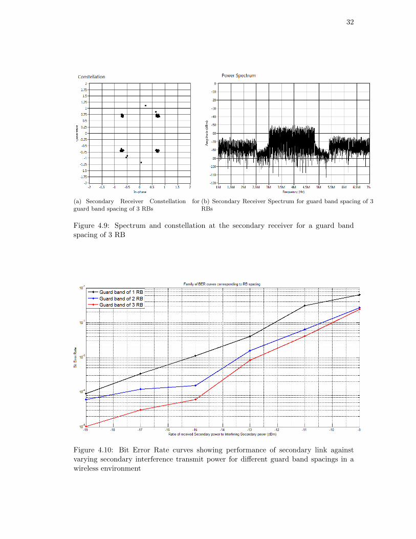
to the interfering secondary transmission have been shown in Figs. 4.7, 4.8, 4.9. Again
the Interfering Secondary Transmission power was increased and its effects were ob-
served on the other secondary link for different guard band spacings. The family of
BER curves of the secondary link for different guard bands seen in the linear range are
shown in Fig. 4.10.

28
Figure 4.2: Spectrum showing coexistence of two secondary users within the same 20MHz band
4.4 Effect of using modified Secondary Transmission techniques on
the suppression
In order to ensure better suppression gain in the Interference Band, modified NC OFDM
transmission techniques like the IA-PFT had been simulated on a MATLAB platform.
The size of the FFT used was 2048 with a Cyclic Prefix of 512. The notch was assumed
to be having a size of 12 Resource Blocks (RBs) corresponding to 144 carriers. Two
AIC tones were used on either side to suppress sidelobe interference from the infor-
mation band. These AIC tones were calculated considering sidelobe interference of 10
information bearing sub-carriers on either side of the interference band. Time Win-
dowing was performed using a total overlap size of 300 samples. The results show a
clear suppression of 10-12 dB as compared to the regular NC -OFDM technique. The
spectra can be shown in Figs. 4.11 and 4.12.

29
(a) Secondary Receiver Constellation in thepresence no interfering secondary
(b) Secondary Receiver Spectrum in the presence of interferingsecondary
Figure 4.3: Spectrum and constellation for absence of Interfering Secondary
(a) Secondary Receiver Constellation in thepresence of Interfering Secondary with averagereceived power of -72dBM
(b) Secondary Receiver Spectrum in the presence of InterferingSecondary with average received power of -72dBM
Figure 4.4: Spectrum and constellation in presence of Interfering Secondary
30
(a) Secondary Receiver Constellation in thepresence of Interfering Secondary with averagereceived power of -66dBM
(b) Secondary Receiver Spectrum in the presence of InterferingSecondary with average received power of -66dBM
Figure 4.5: Spectrum and constellation in presence of Interfering Secondary
Figure 4.6: Bit Error Rate curve showing performance of Secondary link against varyinginterfering secondary transmit power in a wireless environment

31
(a) Secondary Receiver Constellation forguard band spacing of 1 RB
(b) Secondary Receiver Spectrum for guard band spacing of 1RB
Figure 4.7: Spectrum and constellation at the secondary receiver for a guard band of 1RB
(a) Secondary Receiver Constellation forguard band spacing of 2 RBs
(b) Secondary Receiver Spectrum for guard band spacing of 2RBs
Figure 4.8: Spectrum and constellation at the secondary receiver for a guard band of 2RB
32
(a) Secondary Receiver Constellation forguard band spacing of 3 RBs
(b) Secondary Receiver Spectrum for guard band spacing of 3RBs
Figure 4.9: Spectrum and constellation at the secondary receiver for a guard bandspacing of 3 RB
Figure 4.10: Bit Error Rate curves showing performance of secondary link againstvarying secondary interference transmit power for different guard band spacings in awireless environment

33
Figure 4.11: Spectrum of NC OFDM transmission, IA-PFT modified NC OFDM trans-mission, and NC OFDM transmission with CC tones added for a notch of bandwidthcorresponding to 3 RB
Figure 4.12: Spectrum of NC OFDM transmission, IA-PFT modified NC OFDM trans-mission, and NC OFDM transmission with CC tones added for a notch of bandwidthcorresponding to 12 RB

34
Chapter 5
Conclusions and Future Work
5.1 Conclusions
This thesis focused on a real time implementation of a Secondary link and also dis-
cussed various parameters to be considered while evaluating coexistence of two or more
secondary links. It has been assumed that the secondary nodes had been allocated
their respective spectra for transmission. More Importance has been given to evalu-
ation of DSA for two or more secondary links to coexist. The effect of interference
of other secondary transmissions on a particular secondary link were studied and ana-
lyzed via BER analysis. It is possible to design a mathematical model based on these
experiments to generalize the effect of secondary interference and thereby characterize
secondary transceiver performance. This mathematical model would be beneficial in
the design of future secondary devices. The guard band spacing has been observed
to influence the effect of interfering secondary transmissions on the performance of a
particular secondary link. Smaller guard band spacing increases the spectrum utiliza-
tion efficiency but also affects the performance of coexisting heterogenous secondary
links. The tradeoff between maximal spectral utilization and Secondary transceiver
performance was better understood by the experiments performed. Implementation of
advanced interference suppression techniques revealed that a suppression gain of 10-12
dB is clearly observed. Additionally, various hardware design related issues and con-
cerns like timing considerations, resource block allocations, among others, were studied
and a more efficient real time secondary transceiver design was implemented.

35
5.2 Future Work
The secondary transceiver setup that has been built that can serve as a testbed for
further experiments. Since most of the design parameters used closely follow the LTE
standards, the future experiments that will be performed using the testbed may yield
results that adhere to industry specific standards. The IA-PFT module design built
on the FPGA can be further improved to achieve more efficient resource allocation
and meeting of the timing constraints. Wireless Experiments can be performed using
IA-PFT modified NC OFDM transmission to observe gain in suppression. Further
experiments can be performed to evaluate the coexistence of more than two coexisting
secondary users.

36
References
[1] W.McCoy, “Overview of the 3gpp long term evolution physical layer,” Whitepaper, Freescale, Jul. 2007.
[2] Chen Sun, Gabriel Porto Villardi, Zhou Lan, Yohannes D. Alemseged, Ha NguyenTran, Hiroshi Harada, “Optimizing Coexistence Performance of Secondary UserNetworks under Primary User Constraints for Dynamic Spectrum Access,” inTranscations in Vehicular technology, pp. 1-2, Jun. 2012.
[3] Juncheng Jia, Qian Zhang, “A Non-Cooperative Power Control Game for Sec-ondary Spectrum Sharing,” in International Conference on Wireless Communi-cations and Signal Processing, pp. 5933-5935, Nov. 2009.
[4] S. Pinagapany, S. Sequeira, A. Bindiganavile, Y. Futatsugi, M. Ariyoshi, andP. Spasojevic, “Experimental Evaluation of Interference Avoidance Opportunis-tic Secondary Transmission for Coexistence with Primary Systems,” in SDR11WinnComm, 2011.
[5] Poramate Tarasak, Francois Chin, Zhiwei Lin, Xiaoming Peng,“Further Enhance-ment for Active Interference Cancellation on MB-OFDM UWB Transmission,”in Vehicular Technology Conference, pp. 1-4, Sept. 2008.
[6] Yasunori Futatsugi and Masayuki Ariyoshi“Interference Avoidance Transmissionby Partitioned Frequency- and Time-domain Processing,” in Vehicular TechnologyConference, pp. 1-4, 2012.
[7] S. Pinagapany, “Decentralized Spectrum Allocation Schemes for Cognitive RadioNetworking,” Masters thesis, Rutgers, The State University of New Jersey, 2011.
[8] A. Bindiganavile, “Experimental Evaluation of Secondary NC-OFDM Transceiverfor Coexistence with Primary Transmitter,” Masters thesis, Rutgers, The StateUniversity of New Jersey, 2012.
[9] “National Instruments LabVIEW Real Time Controller Platform,” http://www.
ni.com/labview/realtime/.
[10] “NI PXIe RT Embedded Controller Setup,” http://sine.ni.com/nips/cds/
view/p/lang/en/nid/208834.
[11] J.-J. van de Beek, M. Sandell, and P. O. Borjesson, “Ml estimation of timing andfrequency offset in OFDM systems,” in IEEE Transcations on Signal Processing,pp. 1801-1805, Jul. 1997.
[12] LabVIEW FPGA Module User Manual.

37
[13] Buracchini E., “The software radio concept,” in Communications Magazine,IEEE, pp. 2638, Sept. 2000.