Embed Size (px)
Citation preview

8/3/2019 FamilyOfZVS PWMActive Clamping DC DC Converters
http://slidepdf.com/reader/full/familyofzvs-pwmactive-clamping-dc-dc-converters 1/7
698 IEEE TRANSACTIONS ON CIRCUITS AND SYSTEMS—I: FUNDAMENTAL THEORY AND APPLICATIONS, VOL. 44, NO. 8, AUGUST 1997
A Family of ZVS-PWM Active-Clamping DC-to-DCConverters: Synthesis, Analysis, Design, and
ExperimentationClaudio Manoel C. Duarte, Student Member, IEEE , and Ivo Barbi, Senior Member, IEEE
Abstract— This paper presents a technique to generate a com-plete family of two-switch pulsewidth-modulated (PWM) withactive clamping dc/dc converters, featuring soft commutation of the semiconductors at zero-voltage (ZVS). The main purposeof this technique is to integrate these converters under a sametheoretical principle to derive the topologies in a comprehensiveform and generate new circuits. All the converters have theadvantage of soft commutation (ZVS) with minimum switchvoltage stress due to the clamping action. Besides operating atconstant frequency and with reduced commutation losses, theseconverters have output characteristics similar to the PWM hard-switching counterpart, which means that there is no circulatingreactive energy that would cause large conduction losses. Princi-ple of operation, theoretical analysis, simulation and experimentalresults of one particular converter taken as an example, areprovided in this paper.
Index Terms— Active clamping, dc-to-dc converters, powersupplies, soft commutation.
I. INTRODUCTION
T HE TWO TRANSFORMER active reset circuits pre-sented in [1] and shown in Fig. 1 were employed in a
Forward converter to operate over a wide input voltage range.
These circuits recover transformer magnetizing and leakageinductance energies, reduce dc ux in the core, and minimizepeak voltage on the power transistor. One of these circuits,Fig. 1(b), was employed in a Flyback converter [2] to achievesoft switching too. In [3], the other circuit, Fig. 1(a), wasemployed in a Forward converter with some modicationsand the soft switching was obtained too. The circuit shownin Fig. 1(a) was used in [4] as a switched snubber for theswitch and the diode of high frequency PWM converters.In [5], the interrelationships among two switch soft-switchedconverters were analyzed and a generalization was searchedby a generalized two-switched converter.
In this paper, the concept of fundamental ZVS-PWM cellswas employed to generate a complete family of two-switchclamped mode ZVS-PWM dc-dc converters. This techniqueallows the generation, in a comprehensive form, of six basic
Manuscript received October 2, 1996; revised March 27, 1997. This paperwas recommended by Guest Editors A. Ioinovici, L. Martınez-Salamero, andJ. Vlach.
C. M. C. Duarte is with the Engineering School, UCPel-Catholic Universityof Pelotas, 96010-000-Pelotas-RS, Brazil.
I. Barbi is with the Power Electronics Institute-INEP, Federal University of Santa Catarina, 88040-970-Florian opolis-SC, Brazil.
Publisher Item Identier S 1057-7122(97)05820-0.
(a) (b)
Fig. 1. (a) Forward converter with a transformer active reset circuit (1). (b)Forward converter with a transformer active reset circuit (2).
(a) (b) (c)
(d) (e) (f)
Fig. 2. (a) Clamped mode ZVS-PWM forward converter (boost). (b)Clamped mode ZVS-PWM Buck converter (boost). (c) The ZVS-PWMcommutation cell (boost) taken from the buck converter. (d) ClampedMode ZVS-PWM forward converter (buck-boost). (e) Clamped modeZVS-PWM Buck converter (buck-boost). (f) The ZVS-PWM commutationcell (buck-boost) taken from the Buck converter.
family converters. The generation of the cells is describedhereafter.
II. GENERATION OF THE NEW FAMILY OF CONVERTERS
A. Generation of Six Fundamental Clamped Mode ZVS-PWM Cells
Let us consider the Fig. 2, where two ZVS-PWM commu-tation cells are obtained. From the two Forward convertersshown in Fig. 2(a) and (d) it is possible to derive two Buck converters as shown in Fig. 2(b) and (e), and, from these con-verters, like in Hard-switched PWM converters, it is possible
1057–7122/97$10.00 © 1997 IEEE
8/3/2019 FamilyOfZVS PWMActive Clamping DC DC Converters
http://slidepdf.com/reader/full/familyofzvs-pwmactive-clamping-dc-dc-converters 2/7
DUARTE AND BARBI: A FAMILY OF ZVS-PWM ACTIVE-CLAMPING 699
(a) (b)
(c) (d)
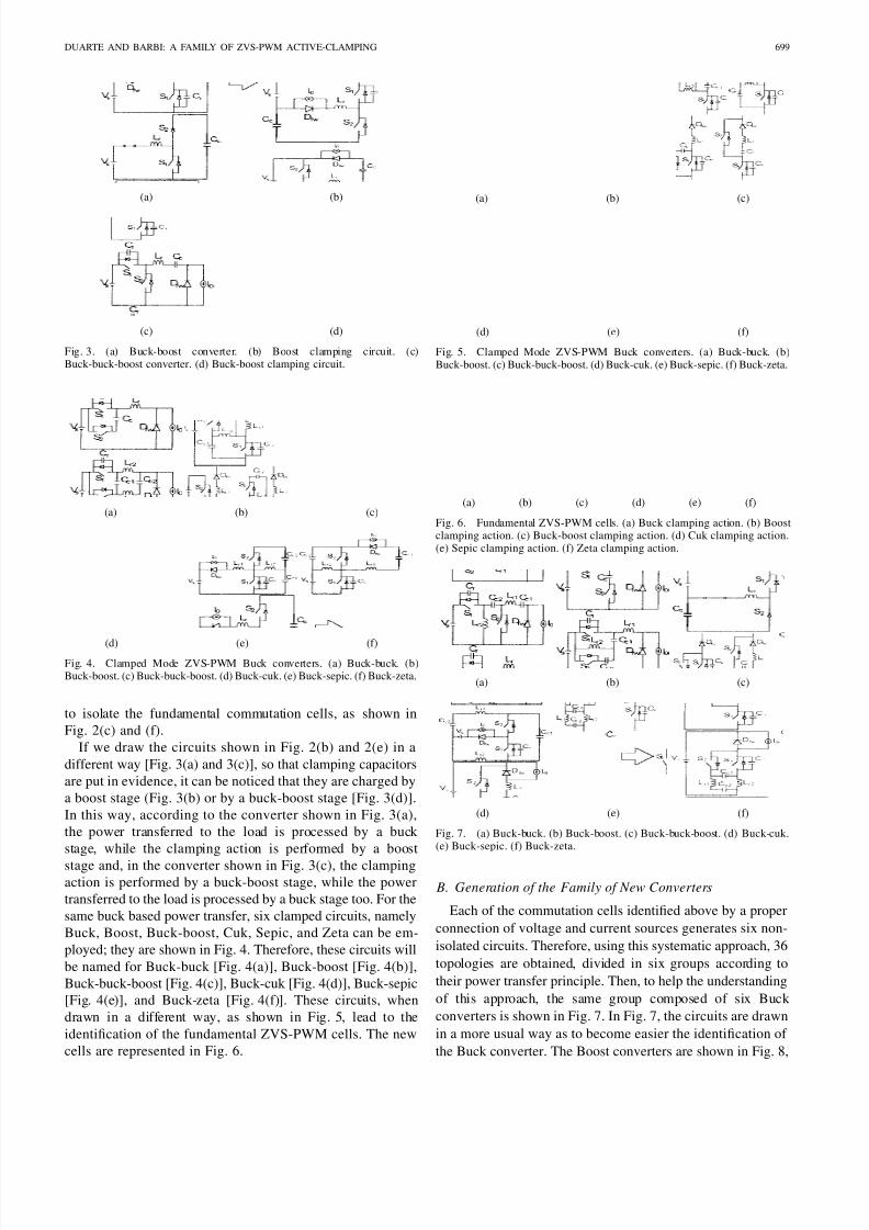
Fig. 3. (a) Buck-boost converter. (b) Boost clamping circuit. (c)Buck-buck-boost converter. (d) Buck-boost clamping circuit.
(a) (b) (c)
(d) (e) (f)Fig. 4. Clamped Mode ZVS-PWM Buck converters. (a) Buck-buck. (b)Buck-boost. (c) Buck-buck-boost. (d) Buck-cuk. (e) Buck-sepic. (f) Buck-zeta.
to isolate the fundamental commutation cells, as shown inFig. 2(c) and (f).
If we draw the circuits shown in Fig. 2(b) and 2(e) in adifferent way [Fig. 3(a) and 3(c)], so that clamping capacitorsare put in evidence, it can be noticed that they are charged bya boost stage (Fig. 3(b) or by a buck-boost stage [Fig. 3(d)].In this way, according to the converter shown in Fig. 3(a),the power transferred to the load is processed by a buck stage, while the clamping action is performed by a booststage and, in the converter shown in Fig. 3(c), the clampingaction is performed by a buck-boost stage, while the powertransferred to the load is processed by a buck stage too. For thesame buck based power transfer, six clamped circuits, namelyBuck, Boost, Buck-boost, Cuk, Sepic, and Zeta can be em-ployed; they are shown in Fig. 4. Therefore, these circuits willbe named for Buck-buck [Fig. 4(a)], Buck-boost [Fig. 4(b)],Buck-buck-boost [Fig. 4(c)], Buck-cuk [Fig. 4(d)], Buck-sepic[Fig. 4(e)], and Buck-zeta [Fig. 4(f)]. These circuits, whendrawn in a different way, as shown in Fig. 5, lead to theidentication of the fundamental ZVS-PWM cells. The newcells are represented in Fig. 6.
(a) (b) (c)
(d) (e) (f)
Fig. 5. Clamped Mode ZVS-PWM Buck converters. (a) Buck-buck. (b)Buck-boost. (c) Buck-buck-boost. (d) Buck-cuk. (e) Buck-sepic. (f) Buck-zeta.
(a) (b) (c) (d) (e) (f)
Fig. 6. Fundamental ZVS-PWM cells. (a) Buck clamping action. (b) Boostclamping action. (c) Buck-boost clamping action. (d) Cuk clamping action.(e) Sepic clamping action. (f) Zeta clamping action.
(a) (b) (c)
(d) (e) (f)
Fig. 7. (a) Buck-buck. (b) Buck-boost. (c) Buck-buck-boost. (d) Buck-cuk.(e) Buck-sepic. (f) Buck-zeta.
B. Generation of the Family of New Converters
Each of the commutation cells identied above by a properconnection of voltage and current sources generates six non-isolated circuits. Therefore, using this systematic approach, 36topologies are obtained, divided in six groups according totheir power transfer principle. Then, to help the understandingof this approach, the same group composed of six Buck converters is shown in Fig. 7. In Fig. 7, the circuits are drawnin a more usual way as to become easier the identication of the Buck converter. The Boost converters are shown in Fig. 8,
8/3/2019 FamilyOfZVS PWMActive Clamping DC DC Converters
http://slidepdf.com/reader/full/familyofzvs-pwmactive-clamping-dc-dc-converters 3/7
700 IEEE TRANSACTIONS ON CIRCUITS AND SYSTEMS—I: FUNDAMENTAL THEORY AND APPLICATIONS, VOL. 44, NO. 8, AUGUST 1997
(a) (b) (c)
(d) (e) (f)
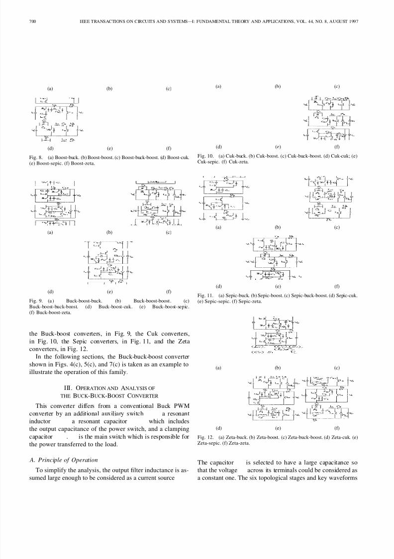
Fig. 8. (a) Boost-buck. (b) Boost-boost. (c) Boost-buck-boost. (d) Boost-cuk.(e) Boost-sepic. (f) Boost-zeta.
(a) (b) (c)
(d) (e) (f)Fig. 9. (a ) Buck-boost-buck. (b) Buck-boost-boost . (c)Buck-boost-buck-boost. (d) Buck-boost-cuk. (e) Buck-boost-sepic.(f) Buck-boost-zeta.
the Buck-boost converters, in Fig. 9, the Cuk converters,in Fig. 10, the Sepic converters, in Fig. 11, and the Zetaconverters, in Fig. 12.
In the following sections, the Buck-buck-boost convertershown in Figs. 4(c), 5(c), and 7(c) is taken as an example toillustrate the operation of this family.
III. OPERATION AND ANALYSIS OFTHE BUCK-BUCK-BOOST CONVERTER
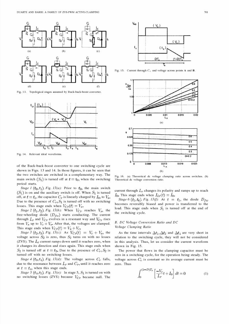
This converter differs from a conventional Buck PWMconverter by an additional auxiliary switch a resonantinductor a resonant capacitor which includesthe output capacitance of the power switch, and a clampingcapacitor . is the main switch which is responsible forthe power transferred to the load.
A. Principle of Operation
To simplify the analysis, the output lter inductance is as-sumed large enough to be considered as a current source
(a) (b) (c)
(d) (e) (f)
Fig. 10. (a) Cuk-buck. (b) Cuk-boost. (c) Cuk-buck-boost. (d) Cuk-cuk; (e)Cuk-sepic. (f) Cuk-zeta.
(a) (b) (c)
(d) (e) (f)
Fig. 11. (a) Sepic-buck. (b) Sepic-boost. (c) Sepic-buck-boost. (d) Sepic-cuk.(e) Sepic-sepic. (f) Sepic-zeta.
(a) (b) (c)
(d) (e) (f)
Fig. 12. (a) Zeta-buck. (b) Zeta-boost. (c) Zeta-buck-boost. (d) Zeta-cuk. (e)Zeta-sepic. (f) Zeta-zeta.
The capacitor is selected to have a large capacitance sothat the voltage across its terminals could be considered asa constant one. The six topological stages and key waveforms
8/3/2019 FamilyOfZVS PWMActive Clamping DC DC Converters
http://slidepdf.com/reader/full/familyofzvs-pwmactive-clamping-dc-dc-converters 4/7
8/3/2019 FamilyOfZVS PWMActive Clamping DC DC Converters
http://slidepdf.com/reader/full/familyofzvs-pwmactive-clamping-dc-dc-converters 5/7
702 IEEE TRANSACTIONS ON CIRCUITS AND SYSTEMS—I: FUNDAMENTAL THEORY AND APPLICATIONS, VOL. 44, NO. 8, AUGUST 1997
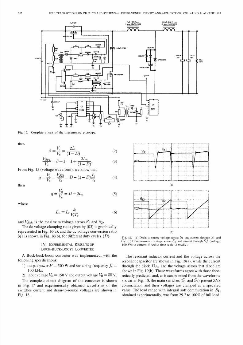
Fig. 17. Complete circuit of the implemented prototype.
then
(2)
(3)
From Fig. 15 (voltage waveform), we know that
(4)
then
(5)
where
(6)
and is the maximum voltage across andThe dc voltage clamping ratio given by (03) is graphically
represented in Fig. 16(a), and the dc voltage conversion ratiois shown in Fig. 16(b), for different duty cycles
IV. EXPERIMENTAL RESULTS OFBUCK-BUCK-BOOST CONVERTER
A Buck-buck-boost converter was implemented, with thefollowing specications:
1) output power 500 W and switching frequency100 kHz;
2) input voltage 150 V and output voltage V.The complete circuit diagram of the converter is shown
in Fig. 17 and experimentally obtained waveforms of theswitches current and drain-to-source voltages are shown inFig. 18.
(a)
(b)
Fig. 18. (a) Drain-to-source voltage across S 1 and current through S
1 andC r . (b) Drain-to-source voltage across
S 2 and current throughS 2 ;
(voltage:100 V/div; current: 5 A/div; time scale: 2 s/div).
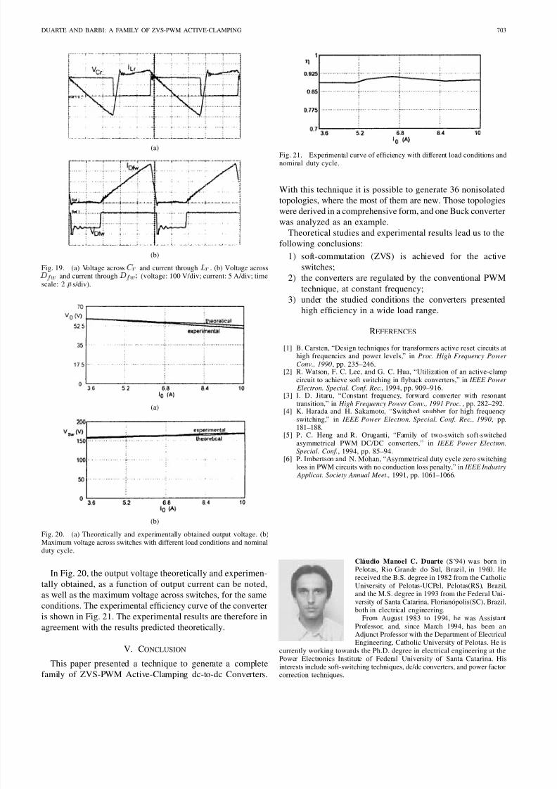
The resonant inductor current and the voltage across theresonant capacitor are shown in Fig. 19(a), while the currentthrough the diode and the voltage across that diode areshown in Fig. 19(b). These waveforms agree with those theo-retically predicted, and, as it can be noted from the waveformsshown in Fig. 18, the main switches ( and ) present ZVScommutation and their voltages are clamped at a speciedvalue. The load range with integral soft commutation inobtained experimentally, was from 29.2 to 100% of full load.
8/3/2019 FamilyOfZVS PWMActive Clamping DC DC Converters
http://slidepdf.com/reader/full/familyofzvs-pwmactive-clamping-dc-dc-converters 6/7
DUARTE AND BARBI: A FAMILY OF ZVS-PWM ACTIVE-CLAMPING 703
(a)
(b)
Fig. 19. (a) Voltage across C r and current through L
r . (b) Voltage acrossD
f w and current through D f w
; (voltage: 100 V/div; current: 5 A/div; timescale: 2 s/div).
(a)
(b)
Fig. 20. (a) Theoretically and experimentally obtained output voltage. (b)Maximum voltage across switches with different load conditions and nominal
duty cycle.
In Fig. 20, the output voltage theoretically and experimen-tally obtained, as a function of output current can be noted,as well as the maximum voltage across switches, for the sameconditions. The experimental efciency curve of the converteris shown in Fig. 21. The experimental results are therefore inagreement with the results predicted theoretically.
V. C ONCLUSION
This paper presented a technique to generate a completefamily of ZVS-PWM Active-Clamping dc-to-dc Converters.
Fig. 21. Experimental curve of efciency with different load conditions andnominal duty cycle.
With this technique it is possible to generate 36 nonisolatedtopologies, where the most of them are new. Those topologieswere derived in a comprehensive form, and one Buck converterwas analyzed as an example.
Theoretical studies and experimental results lead us to thefollowing conclusions:
1) soft-commutation (ZVS) is achieved for the activeswitches;
2) the converters are regulated by the conventional PWMtechnique, at constant frequency;
3) under the studied conditions the converters presentedhigh efciency in a wide load range.
REFERENCES
[1] B. Carsten, “Design techniques for transformers active reset circuits athigh frequencies and power levels,” in Proc. High Frequency Power Conv., 1990 , pp. 235–246.
[2] R. Watson, F. C. Lee, and G. C. Hua, “Utilization of an active-clampcircuit to achieve soft switching in yback converters,” in IEEE Power Electron. Special. Conf. Rec. , 1994, pp. 909–916.
[3] I. D. Jitaru, “Constant frequency, forward converter with resonanttransition,” in High Frequency Power Conv., 1991 Proc. , pp. 282–292.
[4] K. Harada and H. Sakamoto, “Switched snubber for high frequencyswitching,” in IEEE Power Electron. Special. Conf. Rec., 1990 , pp.181–188.
[5] P. C. Heng and R. Oruganti, “Family of two-switch soft-switchedasymmetrical PWM DC/DC converters,” in IEEE Power Electron.Special. Conf. , 1994, pp. 85–94.
[6] P. Imbertson and N. Mohan, “Asymmetrical duty cycle zero switchingloss in PWM circuits with no conduction loss penalty,” in IEEE Industry Applicat. Society Annual Meet., 1991, pp. 1061–1066.
Cl audio Manoel C. Duarte (S’94) was born inPelotas, Rio Grande do Sul, Brazil, in 1960. Hereceived the B.S. degree in 1982 from the CatholicUniversity of Pelotas-UCPel, Pelotas(RS), Brazil,and the M.S. degree in 1993 from the Federal Uni-versity of Santa Catarina, Florian opolis(SC), Brazil,both in electrical engineering.
From August 1983 to 1994, he was AssistantProfessor, and, since March 1994, has been anAdjunct Professor with the Department of ElectricalEngineering, Catholic University of Pelotas. He is
currently working towards the Ph.D. degree in electrical engineering at thePower Electronics Institute of Federal University of Santa Catarina. Hisinterests include soft-switching techniques, dc/dc converters, and power factorcorrection techniques.

8/3/2019 FamilyOfZVS PWMActive Clamping DC DC Converters
http://slidepdf.com/reader/full/familyofzvs-pwmactive-clamping-dc-dc-converters 7/7
704 IEEE TRANSACTIONS ON CIRCUITS AND SYSTEMS—I: FUNDAMENTAL THEORY AND APPLICATIONS, VOL. 44, NO. 8, AUGUST 1997
Ivo Barbi (M’78–SM’90) was born in Gaspar,Santa Catarina, Brazil, in 1949. He received theB.S. and M.S. degrees in electrical engineering fromthe Federal University of Santa Catarina, Brazil, in1973 and 1976, respectively, and the Ph.D. degreefrom the Polytechnic National Institute of Toulouse,France, in 1979.
He founded the Brazilian Power Electronics So-ciety and the Power Electronics Institute of theFederal University of Santa Catarina, where he
currently works as a Professor.Dr. Barbi was an Associate Editor in the Power Converters area of the
IEEE TRANSACTIONS ON INDUSTRIAL ELECTRONICS from 1992 to 1996.