Embed Size (px)
Citation preview
Femtosecond Carrier Dynamics In 111-V Semiconductors Grown
At Low Substrate Temperatures
by
Yiorgos K. Kostoulas
Submitted In Partial Fulfillment of the
Requirements for the Degree
Reviewed for Classification Doctor of Philosophy
Authorized Derivative Chssiffsl Supervised by
Professor Philippe M. Fauchet
Department of Physics and Astronomy The College
Arts and Sciences
University of Rochester Rochester, New York
11
Curriculum Vitae
Yiorgos Kostoulas was born on August 26, 1966. He attended the
Aristoteleio Panepistimio Thessalonikis in Greece from 1984 to 1989, were he
received a Bachelor of Science Degree in Physics. After an internship at CERN, in
the summer of 1989, he started graduate studies in the University of Rochester on
September 1989, under the guidance of Professor A. Melissinos. In 1989 he was
awarded the Erasmus Fellowship and in 1993-1994 he was a recipient of the Link
Foundation Fellowship. His research work has included the Brookhaven National
Laboratory Experiment 840 -a coherent production of any pseudoscalar (or scalar)
that couples to two photons- from May 1989 to December 1990. Subsequently he
directed his efforts in the field of Optical Nonlinearities in 111-V Semiconductors.
Among the areas he has worked on are: Femtosecond Nonlinearities and Hot
Carrier Dynamics in GaAs, Refractive Index Spectral hole burning in InP,
Femtosecond Carrier Dynamics in Porous Silicon, and Sub-Picosecond Carrier
Trapping Times In 111-V Compounds Grown At Low Substrate Temperatures,
from May 1992 to present. He was a teaching assistant in the Department of
Physics from January 1993 to May 1993. This work was supervised by Professor
Philippe M. Fauchet.
Acknowledgments
This work wouldn't have been possible without the support of the
Laboratory of Laser Energetics and the Center for Optoelectronics and Imaging.
Both LLE and COI provided us with facilities and personnel so there are numerous
people to thank: Shirley Steinberg, Ronda Salomon, Dick Fellows, Linda Clement,
LaDona Black and everybody in the electronics shop. This support was matched
by the people of the Physics Department: Betty Cook, Barbara Warren, Ovide
Coriveau, Marj Chapin, and Kenn Harper. I would also like to express my
gratitude to the faculty of the Department of Physics both for instruction during
the years I spend in the University of Rochester and for the insights that I will
carry with me as I move onward. The interactions and collaborations that I have
enjoyed with fellow students and staff have also been invaluable. I am grateful to
Dr. John Soures of LLE, to Prof. Dan Watson for his support and encouragement
during my stay in Rochester, to Prof. Gary Wicks for making all his resources
readily available, and to my advisor Prof. Philippe Fauchet for his continuus
guidance. I would also like to thank Mike Koch for making his expertise in MBE
always available. My appreciation goes to my fellow graduate students Karnil
Burak ~ ~ e r and Ahmad Ibrahim Lobad whose help would be hard to overestimate.
Finally, my special thanks go to my parents, Dionysia and Kostas, whose support
eventhough from a distance, has made this thesis possible.
ABSTRACT
Studies on carrier dynamics, trapping and recombination are presented, in
111-V compounds grown at low substrate temperatures (LT-IIINs). We have used
femtosecond pump-probe, and up-conversion luminescence spectroscopy in order
to determine the dynamics of photoexcited carriers in a variety of semiconductor
compounds of the As and P family (LT-GaAs, LT-InP and LT-GaInP). Changes in
the absorption coefficient and refractive index are measured over a wide spectral
range (570 nm - 900 nm) and at different injected carrier densities (-1016 - 1019
cm-3).
Complementary experimental techniques such as pump-probe and up-
conversion luminescence, show that in the low temperature grown 111-V
compounds, it is carrier trapping that takes place in a sub-picosecond time scale
with carrier recombination following at longer times. In spite of their different
electrical properties, these materials show very similar optical response near the
band edge.
No spectral hole burning is observed in the LT-111-V compounds
studied.Carrrier scattering spreads the distribution to the bottom of the conduction
band within our 100 fs time resolution. Carrier trapping leads to induced
absorption due to the photoionization of the defects by the probe photons. For the

lowest growth temperatures. the trapping times were found to be 0.45 ps. 0.35 ps.
for InP and GaInP grown at 200°C. and 1.4 ps for GaAs as grown at 195OC .
Table of Contents
................................................................................................. Curriculum Vitae ii ... ............................................................................................... Acknowledgments m
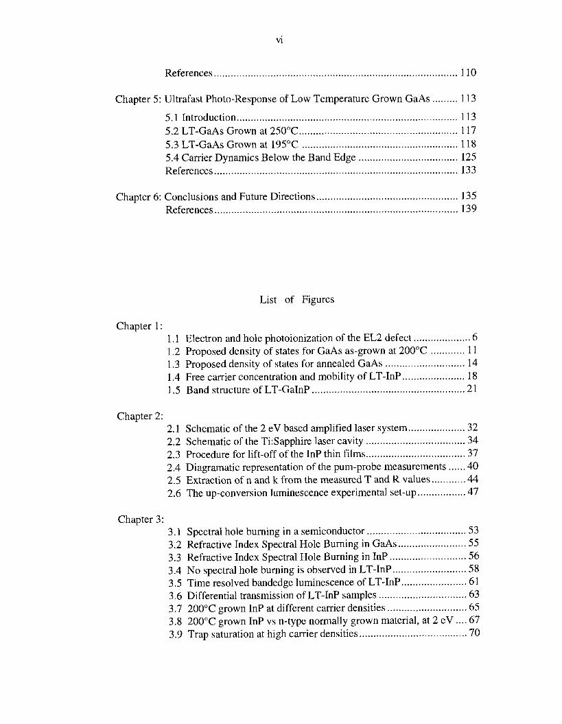
Abstract .............................................................................................................. iv ..................................................................................................... List of Figures vi
List of Tables ..................................................................................................... vii
Chapter 1: Introduction ........................................................................................ 1
1.1 Technological Motivation ............................................................. 1 1.2 Survey of the Material Properties .................................................. 5 1.3 Outline of 'Thesis ......................................................................... 25 References ........................................................................................ 26
Chapter 2: Experimental (:onsiderations ............................................................. 31
2.1 Laser Systems ............................................................................. 31 ..................................................................... 2.2 Sample Preparation 35
2.3 Experimental Methods ................................................................ 38 References ........................................................................................ 48
Chapter 3 : Femtosecond Carrier Dynamics In Low Temperature Grown InP ...... 50
3.1 Introduction ................................................................................ 50 3.2 Refractive Index Spectral Hole Burning ...................................... 52 3.3 Carrier Trapping and Recombination ........................................... 59 References ........................................................................................ 72
Chapter 4: Carrier Dynamics In low Temperature Grown Gag 5 1Ino 49P Above and Below The Conduction Band Edge ............................................. 75
................................................................................ 4.1 Introduction 75 4.2 Carrier Dynamics In Conventionally Grown GaInP ..................... 77 4.3 Carrier-Carrier Scattering In Conventionally Grown GaAs and
GaInP ......................................................................................... 86 4.4 Carrier Dynamics In Low-Temperature Grown GaInP ................ 96 4.5 Spectral Hole Burning In Conventionally and Low Temperature
Grown GaInP ........................................................................... 101 4.6 Carrier Trapping vs Recombination In Low-Temperature Grown
GaInP .................................................................................... 104 4.7 Conclusions .............................................................................. 109
References ...................................................................................... 1 10
Chapter 5: Ultrafast Photo-Response of Low Temperature Grown GaAs ......... 113
.............................................................................. 5.1 Introduction 113 5.2 LT-GaAs Grown at 250°C ........................................................ 117 5.3 LT-GaAs Grown at 195OC ....................................................... 118 5.4 Carrier Dynamics Below the Band Edge ................................... 125
...................................................................................... References 133
.................................................. Chapter 6: Conclusions and Future Directions 135 ...................................................................................... References 139
List of Figures
Chapter 1: 1.1 Electron and hole photoionization of the EL2 defect .................... 6 1.2 Proposed density of states for GaAs as-grown at 200°C ............ 11 1.3 Proposed density of states for annealed GaAs ............................ 14 1.4 Free carrier concentration and mobility of LT-InP ...................... 18 1.5 Band structure of LT-GaInP ...................................................... 21
Chapter 2: .................... 2.1 Schematic of the 2 eV based amplified laser system 32
................................... 2.2 Schematic of the Ti:Sapphire laser cavity 34
................................... 2.3 Procedure for lift-off of the InP thin films 37 ...... 2.4 Diagramatic representation of the pum-probe measurements 40
............ 2.5 Extraction of n and k from the measured T and R values 44 ................. 2.6 The up-conversion luminescence experimental set-up 47
Chapter 3: 3.1 Spectral hole burning in a semiconductor ................................... 53 3.2 Refractive Index Spectral Hole Burning in GaAs ........................ 55 3.3 Refractive Index Spectral Hole Burning in InP ........................... 56
.......................... 3.4 No spectral hole burning is observed in LT-InP 58 ....................... 3.5 Time resolved bandedge luminescence of LT-InP 61
3.6 Differential transmission of LT-InP samples ............................... 63 3.7 200°C grown InP at different carrier densities ............................ 65 3.8 200°C grown InP vs n-type normally grown material. at 2 eV .... 67
...................................... 3.9 Trap saturation at high carrier densities 70

Chapter 4: 4.1 Band edge luminescence of conventionally grown GaInP ........... 78
........... 4.2 Carrier dynamics at 2 eV in conventionally grown GaInP 81 ........ 4.3 2 eV/WLC measurements of conventionally grown GaInP 85
............. 4.4 Carrier-carrier scattering in GaAs at low carrier density 89 ............ 4.5 Carrier-carrier scattering in GaAs at high carrier density 91 ........... 4.6 Carrier-carrier scattering in conventionally grown GaInP 94
............. 4.7 AT,, vs carrier density in conventionally grown GaInP 95 ........................................ 4.8 Carrier dynamics in LT-grown GaInP 98
......... 4.9 Response of 200°C grown GaInP at 620 nm and 750 nm 100 4.10 Spectral hole burning in conventionally and LT-grown GaInP . 103
... 4.1 1 300°C and conventionally grown GaInP response at 840 nm 105 4.12 Response of 200°C as-grown and annealed samples (840 nm) . 108
Chapter 5: 5.1 2 eV/WLCI measurements on 250°C as-grown GaAs ................ 116 5.2 2 eV/WLC: measurements on 195°C as-grown GaAs ................ 119 5.3 Single exponential fit of the 890 nm response ........................... 121 5.4 2 eV/WLC measurements on 195°C aannealed GaAs ............... 122 5.5 Comparison of the banedge response of four GaAs samples ..... 124
..... 5.6 1.55 eV/WLC measurements on the 195°C as-grown GaAs 126 ...... 5.7 1.55 eV/WLC measurements on the 195°C annealed GaAs 128 ..... 5.8 1.55 eV/WLC measurements on the 250°C as-grown GaAs 130
.......... 5.9 1.55 eV/WLC measurements on the 500°C grown GaAs 131
Chapter 6: .... 6.1 Expected behavior of other 111-Vs grown at lowtemperature 138
List of Tables
Chapter 1 : Table I Photoconductive Materials With Carrier Lifetimes and
............................................................................ Mobilities 3 Table I1 Material Parameters of Annealed LT-GaAs ........................ 16
Chapter 4: ........................ Table I11 Material Parameters for GaInP and GaAs 79
1
CHAPTER 1
Introduction
1.1 Technological Motivation
The development of ultrashort optical pulses has lead to the emergence of
new techniques for the generation and detection of subpicosecond electrical
transients. Laser-triggered, ultrafast photoconductive switching [l] and electro-
optic sampling [2] are techniques that have demonstrated a capability for
subpicosecond or near-terahertz responselbandwidth. Currently, the limitations
imposed on these techniques are mainly due to the long lifetime of the photo-
generated carriers. To achieve significantly shorter carrier lifetimes, various
methods have been employed in the past with different degrees of success. A
partial list includes introduction of deep levels through doping with compensating
impurities, use of amorphous or polycrystalline [3] materials, bombardment with
high-energy particles and ion implantation, and use of 11-VI materials such as
CdTe grown by metal-organic vapor phase epitaxy (MOVPE) [4]. Unfortunately
all of these methods suffer from inherent limitations. For instance, doping with
compensating impurities introduces deep levels and hence reduces the carrier
lifetime. In the case of GaAs:Cr, carrier lifetimes of -60 ps have been found [5].
While shorter than for intrinsic materials, the lifetimes realized by this process limit
the electrical pulse widths that can be generated to a few tens of picoseconds.
In the case of the amorphous and polycrystalline materials, it is their low
carrier mobility that acts as the limiting factor. Amorphous silicon is one such
material that has been extc:nsively studied as a photoconductor [6]. However, due
to disorder, the charge transport takes place through the extended band tail states,
resulting in a very low drift mobility (-1 cm2/vsec). This implies a poor
conversion efficiency from the applied bias to the peak amplitude of the generated
pulse.
The use of damage induced by high energy particles in order to create deep
level trappinglrecombination centers can also lead to short carrier lifetimes. For
instance, the free-carrier lifetime in O+ implanted Si-on-Sapphire (SOS) decreases
as the implantation dose increases. In studies of SOS experiencing doses above
3x1014 cm-2, the measured carrier lifetime reached a limit of 600 fs [7]. Proton
bombardment has been also used to decrease the carrier lifetime in InP and GaAs.
Carrier lifetimes reaching down to -100 fs for very high doses of - l o 6 have
been reported in the case of InP [8]. Two problems are associated with this
technique: First, as the implantation dose increases, the carrier mobility decreases
leading to low responsivil:y, a problem similar to that encountered in amorphous
materials, and second, the degradation of the ion-implanted materials at room
temperature.
Very fast switching times (-480 fs) have been achieved with 11-VI
materials, such as CdTe.[Sl] In addition the responsivity of this material is relatively
high since the carrier mobility is -1 80 cm%sec. The main problem is the difficulty
Table I. Photoconductive materials with carrier lifetimes and mobilities.
- -- p-,~~p----%
Material Carrier Lifetime (ps) Mobility (cm2/v s)
GaAs:Cr
Ion-implanted InP
Ion-damaged SOS
Amorphous silicon
MOCVD CdTe
Table I. Various photoconductive materials with their carrier lifetimes and mobilities. (After Gupta et. al., IEEE J Quantum Electron., QE-28, 2464 (1992).
to integrate 11-VI materials with the relatively mature 111-V semiconductor device
technology. Table I lists some of these materials and their typical lifetimes together
with their mobilities.
An alternative approach that seems to overcome the above limitations is
the growth of 111-V semi~conductors at low substrate temperatures. For epitaxial
growth of 111-V semiconductor layers by molecular beam epitaxy (MBE), the
substrate temperature Tg, the group VIIII flux ratio and the growth rate are the
important parameters determining the growth mechanism and the quality of the
epitaxial layers. Varying the growth temperature in order to optimize growth
conditions, has been used extensively. Between 1978 and 1983 a small number of
papers([lO, 111) reported the first attempts to grow GaAs at substrate
temperatures lower than the standard 600°C but at the same growth rate. The
resulting material exhibited an abrupt decrease in mobility and carrier
concentration, and was also "optically dead" (i.e. it was not luminescent). Colin
Wood, one of the pioneers in MBE, would refer to this type of GaAs as
"wooden", perhaps in reference to his early crystal growths. In order to
compensate, Metze and Calawa [12] reduced the growth rate and defined the
growth conditions [13] for what is now known as LT-GaAs: Tg of about 200°C,
growth rate of about 1 pm/h and As-stable growth conditions (As:Ga beam
equivalent pressure ratio of 10: 1). This type of material has a high density of point
defects, due to the growth at low temperature. These defects act as
trappinglrecombination centers, reducing the carrier lifetime to -400 fs. The
resulting material is also of high crystalline quality (the low growth rate allows
enough time to the ad-atoms to move to their lattice sites) and therefore of high
carrier mobility (F-1000 cm2/V-sec). These properties, together with high
resistivity (after annealing at 600°C for 10 minutes) make this material the most
suitable candidate for the opto-electronic applications mentioned earlier, without
any of the deficiencies encountered in the previous attempts to shorten the carrier
lifetime.
This success has led to the commercialization of LT-GaAs based, high-
speed optoelectronic devices as is demonstrated by the spin-off of Picometrix, Inc.
Additionally, other 111-V materials such as LT-InP, InGaP, AlGaAs, InAlAs and
InGaAs have been investjgated in an effort to understand better the fundamental
properties of these co~mpounds and to identify candidates suitable for
optoelectronic devices at the optical communications wavelength of 1.55 Fm. In
this work we will concentrate on three different 111-Vs that have very different
electrical properties when grown at low substrate temperatures: LT-InP, LT-
Gag 5 1 In0 49P, and LT-CiaAs.
1.2 Survey of the Material Properties
LT-GaAs
The dominant point defects in LT-GaAs are EL2-related defects. In an attempt to
supply a background for the understanding of the material properties of LT-GaAs,
we summarize the major characteristics of the EL2 defect in GaAs. The EL2 defect
is the dominant defect in melt grown GaAs. It is commonly present in
concentrations of 1 - 2 x 1 0 ~ ~ cm-3 both in liquid encapsulated Czochralski (LEC)-
and Bridgman-grown crystals. EL2 is present in concentrations of 1014 cm-3 in
vapor phase epitaxy (VP'E) GaAs. However, it is not present in liquid phase
epitaxy (LPE) grown layers or in molecular beam epitaxy (MBE) layers (the
defects in LT-GaAs are EL2-like, i.e. they exhibit most but not all of the EL2
properties). The EL2 defect basically controls the electrical and optical properties
of GaAs and its existence makes it possible to achieve thermally stable semi-
insulating (SI) GaAs-the key material in integrated circuit technology.
The EL2 defect is created under As-rich conditions. Its concentration can
be controlled to some extent by stoichiometry during crystal growth. For the range
of AsIGa over which monocrystalline (melt grown or epitaxial) GaAs can be
grown, the concentration[ of EL2 varies by less than an order of magnitude.
Lagowski et al. [14] linked EL2 with an arsenic antisite defect. ASG, has a double
donor character, and according to the mass action law its creation can be strongly
suppressed by intentional doping with shallow donors. This leads to a variation of
the EL2 concentration by more than three orders of magnitude (nearly constant at
-1016 cm-3 for a free electron concentration up to 5x1016 cm-3 and reducing to
less than 1013 cm-3 when the free electron concentration exceeds 2 x 1 0 ~ ~ ~ r n - ~ ) .
These results lead to a two-step mechanism for the creation of the EL2 defect:
i . the creation of Ga vacancies under As-rich conditions (during GaAs
solidification al. - 1250°C), and
ii. the migration olf As atoms and their interaction with gallium vacancies,
leading to the creation of antisite As-related defects (during post
solidification cooling at -800°C).
The EL2 defect has a deep donor character. The EL2 thermal activation
energy was determined to be at 0.75 eV below the conduction band Ec [15] using
Hall measurements. This means that the ground state of configuration EL~O/+ is
roughly placed in the middle of the GaAs energy gap (EL~O/+ represents EL2 in
the neutral charge state when the Ec-0.75 eV level is occupied and in the singly
positive charge state after giving up an electron). The second ionization level,
EL^+/++, lies at 0.52 eV aibove the top of the valence band
The near infrared absorption spectrum related to EL2 in neutral charge
state was first published by Martin [16]. After the part corresponding to the
intracenter transitions was identified (between 1.0 eV and 1.3 eV) [17], the
spectrum corresponding to photo-ionization of the EL2 was isolated. It consists of
three bands with energy thresholds at about 0.8 eV, 1.0 eV and 1.3 eV, related to
photo-ionization to the T., L, and X points of the GaAs Brillouin zone. The EL2
optical cross section, both for photo-ionization to the conduction band (EL~O +
EL2+ + e in the conduction band) ono, and for electron capture from the valence
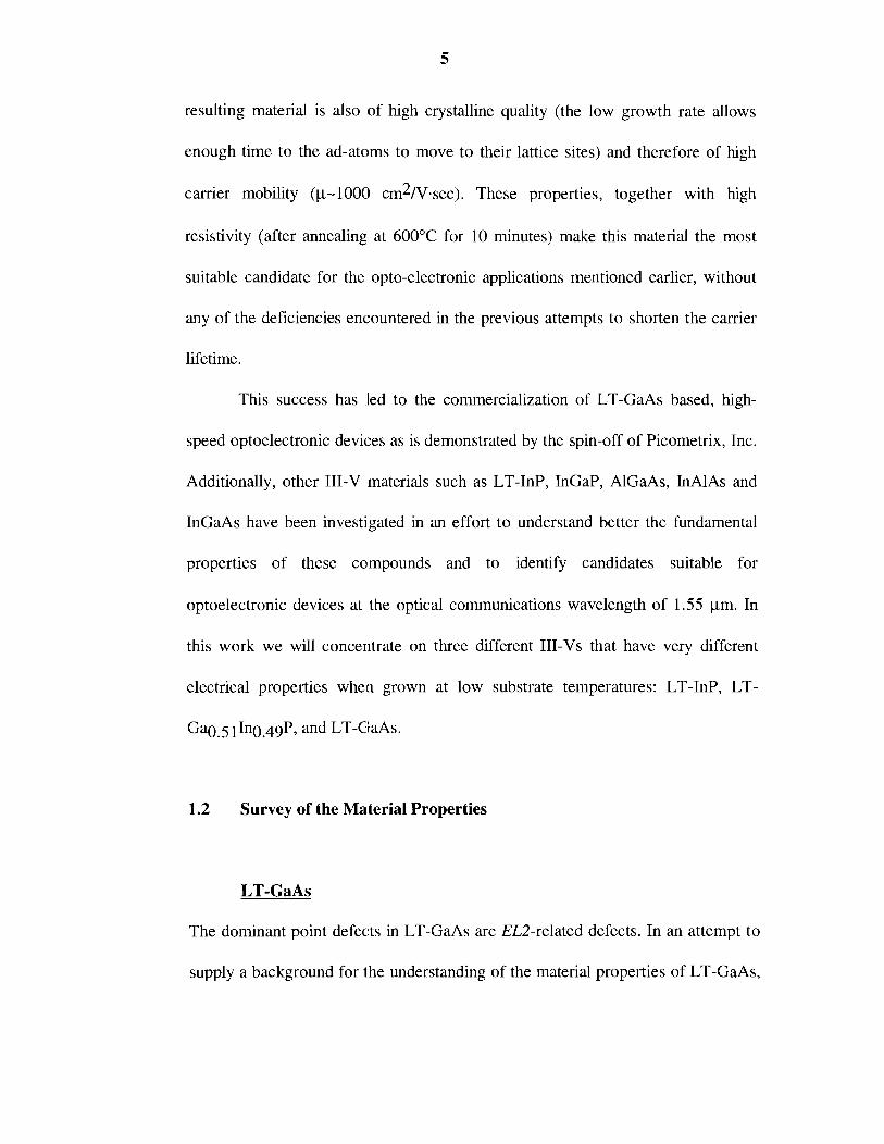
band (EL2+ + e in the valence band + EL~O) 4°, was determined by Silverberg
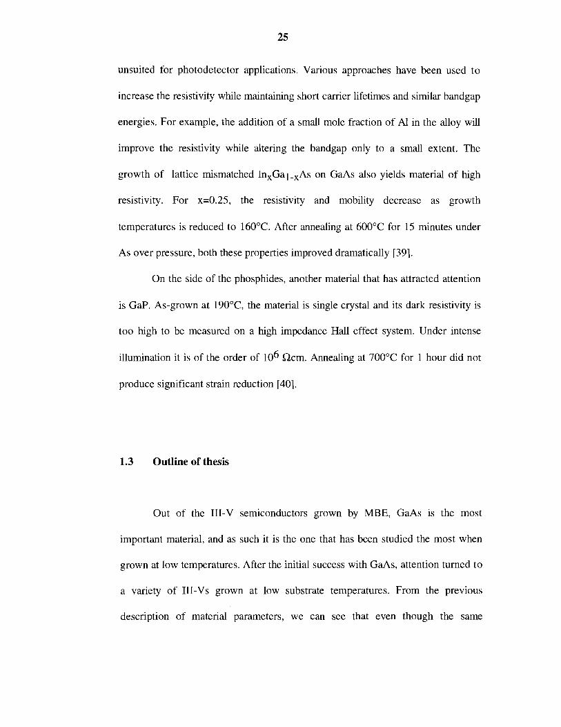
et a1 [18]. Their data for rloom temperature can be seen in Figure 1.1. The cross
22020 Photon energy (eV)
Figure 1.1 Room temperature electron (squares) and hole (circles) cross- sections of the EL2 in GaAs (After Silverberg et. al. [18]).

section at room temperature, for 1.2 eV photons, is 0.3~10-16 cm2 and
16 2 10- cm for hole and e:lectron photo-ionization respectively.
The most characteristic feature -the signature- of the EL2 defect is its
metastable state. It occurs; at low temperatures (<I30 K) under illumination with
light of 1 .O- 1.3 eV. Its spectrum is identical to the intracenter absorption spectrum.
The EL2 transition from its neutral ground state to the metastable state occurs
without change of the defect charge state. The de-excitation of the EL2 from its
metastable state takes place thermally and it is accelerated in the presence of free
electrons, due to an "Auger-like" process. Optically induced relaxation of the
metastable state has also been studied but results are not yet conclusive. Due to the
existence of the metastable state, the near infrared absorption of EL2 can be
quenched under illumination with white light.
A theory has been proposed recently in order to explain the metastable
state of the EL2 defect. According to Dabrowski and Scheffler [19] the metastable
transition arises when a neutral AsGa absorbs a photon of -1.1 eV energy and
moves from the Ga lattice site into an interstitial location. This process creates a
VGa-Asi defect complex. A perturbation in the local environment of the defect can
preclude the existence of the metastable state, as has been observed in plastically
deformed and neutron and electron irradiated samples. In these cases, an increase
has been observed in the density of and AsGa+ defects, but the near
infrared absorption is not quenched by white light illumination, i.e. no metastable
state exists. The defects in LT-GaAs are also of similar nature.

In the NIBE growtlh of GaAs, the growth rate is determined by the Ga flux
incident on the sample, while the As flux and the substrate temperature determine
the surface reconstruction.. These three parameters determine if the growing GaAs
surface is As- or Ga- stabilized (i.e. has an excess of As or Ga). As the growth
temperature is reduced, a smaller As-to-Ga flux ratio is needed in order to achieve
As stabilized growth conditions. For the growth of LT-GaAs, it is usually 10: 1
As:Ga, ensuring As-rich conditions. Additionally, the Ga or As adatoms do not
have enough time to movle to their respective equilibrium lattice sites before they
are incorporated into the growing film. These growth conditions lead to an
increased number of defects in the film, such as A s G ~ , V G ~ , and AS^.
In studying LT-G,aAs, we need to distinguish two forms: the as-grown
material and the annealed material, which have quite different properties. The
parameters quoted refer to samples grown at -200°C and the standard annealing
conditions are at 600°C for 10 min under As overpressure.
As more arsenic is incorporated into the sample at low growth
temperatures, the stoichiometry of the material changes. The resulting as-grown
GaAs is found to be lat470-2at% As-rich. This leads to an increase in the lattice
constant by ~aia,-l0-3. The larger lattice constant causes pseudomorphic growth
of the LT epilayer, with a pseudomorphic thickness that reduces with reducing
growth temperature. For 200°C, the pseudomorphic thickness is -2 pm, above
which the epilayer becorrles polycrystalline. The density of the dominant ASG,
defect is -1020 as it was determined by IR absorption. This defect has
an energy level 0.75 eV below the conduction band minimum. Such a large density
of point defects leads to the creation of a defect band via two possible
mechanisms. The first is cidled disorder broadening. In this mechanism, the energy
of the deep levels associated with the defects is perturbed by a change in their local
environment, as, for instance, by some other nearby charged defect or crystal
imperfection. The disordered distribution of these other defects (especially charged
ones) represents a fluctuating potential that shifts the energy levels of the defect
under consideration, leading to an energy spread of the deep levels and the
formation of the deep-level band. The second mechanism involves the wave
function overlap of the defect states. The greater the density of defects, the greater
the wave function overlap, and hence, the greater the spread of the defect energy
band. This is analogous to the tight binding approximation used to describe the
formation of energy bands in crystals. The contribution of this mechanism to the
formation of an AsGa defect band in LT-GaAs is expected to be small since these
defects are spaced, on average, a distance 220 A apart in the as-grown and
annealed material. The width of this band is estimated from conductivity
measurements to be -0.1';' eV in the as-grown material. Of these defects, -5% are
ionized, leading to a concentration of AsGa+ of -5x10¹⁸ ~ m - ~ , as determined by
electron paramagnetic resonance (EPR).
The IR absorption shows the same characteristics as that of the EL2 defect
i.e. it begins at 0.75 eV, and has the two changes of slope observed in the
absorption of EL2. It can be quenched only partially, leading to the conclusion that
only part (-10%) of the: ASG,O defects are EL2 defects. For the as-grown
material, the conduction at room temperature is due to hopping of holes in the
defect band. Therefore, the electrons from the ASG, ionized defects must be
bound to compensating acceptors. The defects that act as such are the Ga
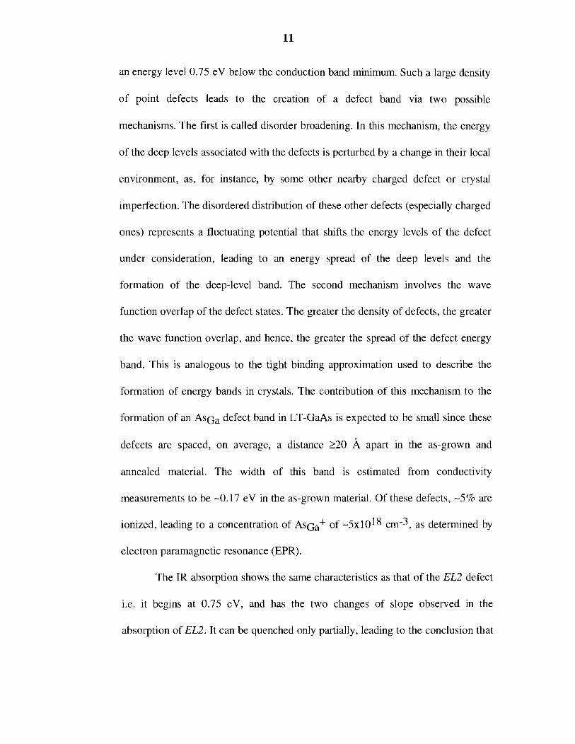
vacancies, VGa, which have an acceptor level at 0.34 eV above the valence band
edge. A density of states diagram for the as-grown material can be seen in Figure
1.2. The room temperatun: resistivity of the as-grown material is low, -100 R cm,
for growth at 200°C.[20] The mechanism responsible for such low resistivity is
nearest neighbor hoppin;: of holes in the 0.75 eV defect band. At higher
temperatures, the conductivity is due to free electrons in the conduction band, with
a mobility of 1000 cm2P~sec. Between 0°C to -90°C, the conductivity can be
described by a temperature activated mechanism resulting in a defect band width of
0.17 eV with a mobility of -1 cm21~sec. At even lower temperatures, the mobility
is again of the order of 1 cm2/Vsec and the conductivity is due to variable range
hopping ( ~ O ~ O - T - ~ I ~ ) .
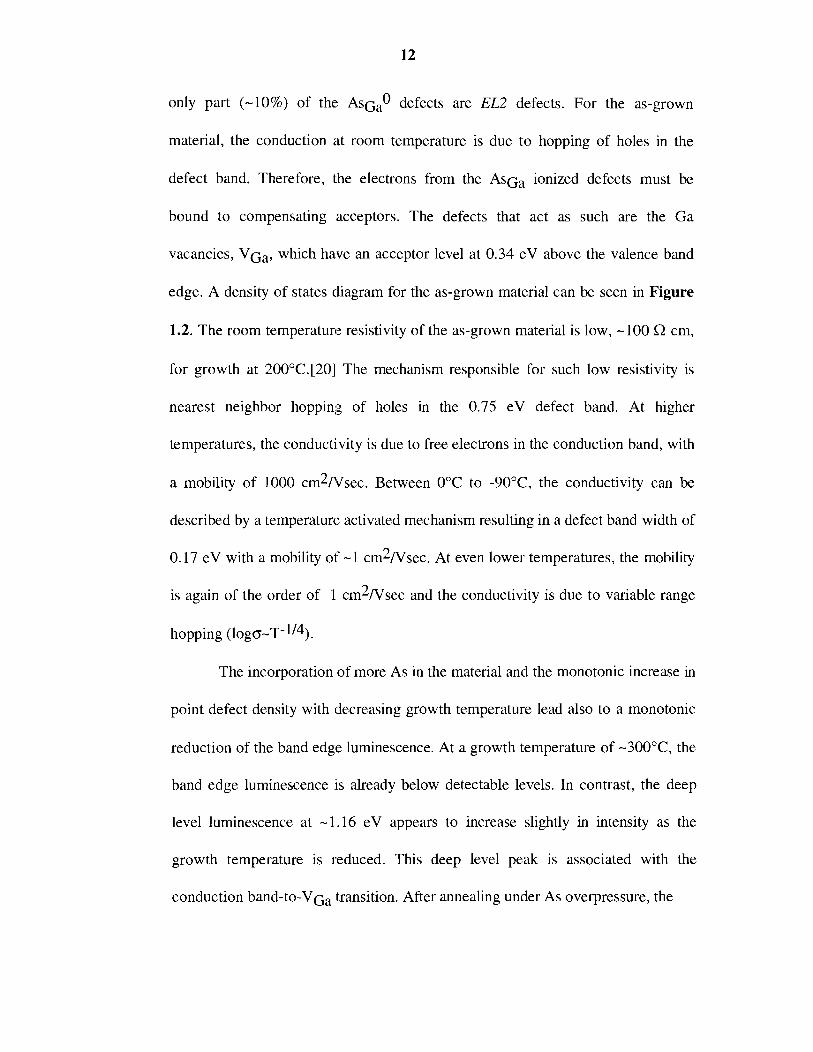
The incorporation of more As in the material and the monotonic increase in
point defect density with decreasing growth temperature lead also to a monotonic
reduction of the band edge luminescence. At a growth temperature of -300°C, the
band edge luminescence is already below detectable levels. In contrast, the deep
level luminescence at -1.16 eV appears to increase slightly in intensity as the
growth temperature is reduced. This deep level peak is associated with the
conduction b a n d - t 0 - V ~ ~ transition. After annealing under As overpressure, the

As, (ion channeling, RS) As precipitates (RS)
0.17 eV (conductivity)
$ E~ - -[AsGa+] ' s 5 x 10" cmP3 (EPR) El - - - - - - - - - - - - - - - - El [AsGaO] " lo2' cmP3 (IR)
W
[v,,] = 5 x 1018 cm-3 (RS, EPR, PL) E~ - - - - - - - - E"
I
Density of states Position
(b)
Figure 1.2 Model for as-grown LT-GaAs. (a) Density of states and (b) band diagram. The technniques used to identify the defefcts are shown in parentheseses. R1, R2, and R3 represent nearest neighbor hopping, variable range hopping, and thermal activation conduction (after Smith, F. 'W. PhD Thesis, MIT 1990).

amount of excess As in the epilayer does not change but rather redistributes itself
in the GaAs crystal matrix, and As precipitates are formed [21]. The average
diameter of the precipitates is 60 A and their density is of the order of 1017 cm-3
to 1018 (for higher annealing temperatures and/or longer times, the diameter
of the precipitates as well as their average spacing increases) [22].
The lattice constant is reduced monotonically with increasing annealing
temperature, until it becomes indistinguishable from that of the conventionally
grown material. The density of the A S ~ , O is reduced by about an order of
magnitude, to - 1019 ern-?. The density of AsGa+ drops below levels detectable by
EPR i.e. <1018 ~ m - ~ , but the persistence of hole hopping conductivity at room
temperature indicates that it is still appreciable. As a result of the anneal, the width
of the defect band is also reduced to 0.04 eV. Annealing also leads to a slower
band edge optical response of LT-GaAs. The carrier lifetime increases from -2 ps
to - 10 ps [22] as the average As precipitate diameter increased from 400 A to 900
A, with 30 second anneals at temperatures ranging from 650°C to 1000°C [22].
Annealing of the material leads also to a much higher resistivity of -106 R-cm . A
schematic of the annealed LT-GaAs density of states diagram is depicted in Figure
1.3 and its properties are summarized in Table 11.
Two models have been proposed in order to explain the semi-insulating
properties of the annealed LT-GaAs: the buried Schottky barrier model [23] and
the arsenic antisite defect model [24]. The former explains the semi-insulating
properties in terms of overlapping depletion regions around As precipitates formed

Asl (ion channeling, RS) As precipitates (RS)
0.04 eV (conductivity)
[ A S ~ ~ + I <I 018 cm-3 (EPR) - - - - $ El C [AsGaO] Z- loi9 ~ m - ~ (IR) W
[VGa] <loi8 cmP3 (RS, EPR, PL) E ~ - - - - - - - -
0.34 eV (PL) EV
Density of states
(a) 22022
Position
(b)
Figure 1.3 Model for annealed LT-GaAs. (a) Density of states and (b) band diagram. The technniques used to identify the defefcts are shown in parentheseses. Rl, R2, and R3 represent similar conduction mechanisms as in figure 1.2 (after Smith, F. W. PhD Thesis, MIT 1990).

16
Table 11. Material parameters of annealed LT-GaAs
&-.*-%%%-A "
GaAs Annealed LT-GaAs
Structure Crystalline Crystalline
S toichiometry - 1 at % excess As Ga0.5As0.5
Ga0.495As0.505
Resistivity - 0.3-20 R-cm - lo6 R-cm
Breakdown field - 3 lo4 v cm-I - 5 lo5 ~ c m - I
Trap density < 1015 ~ r n - ~ - 1o19crn-3
Trapping time -1 ns < 1 ps
Table 11. Summary of the material parameters of low tetmperature LT-GaAs grown at -200°C .
upon annealing, while the latter attributes the semi-insulating properties to the
residual ASG, defects which pin the Fermi level close to the mid-gap. The effect of
doping on the dynamics of As clustering in LT-GaAs has also been studied
extensively. It has been observed that the precipitates tend to accumulate in the rz-
doped regions and deplete from the p-doped regions on annealing.
Melloch [25] suggested that the dynamics of cluster formation can be
qualitatively understood based on the charged states of the As interstitial and using
thermodynamic arguments in which the crystal attempts to minimize the chemical
potential during the anneal. The As interstitial has two positive charge states, + I
and +3. It is a "negative U" defect and it goes directly between these two charge
states without a +2 charge state. In n-type material the As-precipitates are
negatively charged and will attract positive As interstitials. In p-type material, the
precipitates are positively charged and will repel positively charged As interstitials.
However, there is still a short range attraction that will allow As precipitates to
form in p-type LT-GaAs. Therefore, during coarsening there will be a preferential
growth of the As precipitates on the n-GaAs side of a pn junction. In addition, a
precipitate in an electric field will not be stable because if it thermally emits an As
interstitial, the interstitial will be swept away by the electric field due to its positive
charge. That explains the formation of As precipitates in Si &doped planes and in
between Be- &doped planes [26] .
LT-InP
InP is the second most important IIIIV binary after GaAs. Because of its
direct band gap, smaller than that in GaAs, it is primarily used for a variety of light
sources and optoelectronic detectors. Its very high carrier mobilities make InP an
attractive material for fabricating high-speed devices. As in the case of GaAs, both
bulk and epitaxial technologies are now mature, economically viable, and allow the
fabrication of structures with properties desirable for commercial applications.
When growth at low temperatures is attempted, the case of InP is quite
different from that of LT-GaAs. Even though the same prescription has
beenfollowed in an effort to create semi-insulating InP layers of good crystalline
quality and short carrier trappinglrecombination time, the resulting material is
heavily n-type [29]. Such high electron concentration in LT-InP is mainly related
to non-stoichiometric effects. The species of native defects in phosphorus-rich InP
are Pi (phosphorus interstitial), PI, (phosphorus antisite defect), and VI, (In
vacancy). Of these only PI, is a donor. Because the phosphorus atom is much
smaller than the In atom, P can easily occupy an In vacancy under P-rich
conditions. This can lead to up to -6% excess P at growth temperatures of 200°C
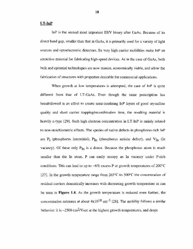
[27]. In the growth temperature range from 265°C to 500°C the concentration of
residual carriers dramatically increases with decreasing growth temperature as can
be seen in Figure 1.4. As the growth temperature is reduced even further, the
concentration saturates at about 4x10¹⁸ [28]. The mobility follows a similar
behavior: it is -2500 cm2/Vsec at the highest growth temperatures, and drops
I 014 100 200 300 400 500
22074 Growth temperature ("C)
Figure 1.4 Room-temperature free carrier concentration n and mobility p in undoped InP epilayers as a function of the growth temperature (from Dreszer et. al. [28]).

down to <500 cm2/Vsec for temperatures between 300°C and 200°C. The defect
responsible for these properties is the PI, interstitial which acts as a double donor.
Its first ionization level, PI,+, which is degenerate with the conduction band at
0.11 eV above the conduction band minimum, has been identified by far infrared
absorption under hydrostatic pressure [28]. This level gives rise to the high
electron concentration via auto-ionization. Its second ionization level, PI,++, lies
at 0.23 eV below theconduction band. l- point [28]. The resistivity of the as-grown
material is very low, -0.02 Qcm at room temperature [29]. Doping with Be, in an
attempt to create semi-insulating LT-InP, has not achieved the desired results. The
material remains n-type even at the highest doping densities of - 1 0 ~ 9 [29].
Ex-situ annealing of as-grown LT-InP at 500°C for 30 min can lead to an increase
in resistivity of the undoped and Be-doped material by a factor of 6 and 60
respectively [29]. The formation of phosphorus precipitates has also been observed
[30,3 11. They consist of the alpha-white cubic form of phosphorus [3 11 which is
insulating and their size ranges from 3 nm [31] up to 50 nm [30] for annealing at
-600°C for a few minutes.
Gag 491110 5 1P (hereafter referred to as GaInP), with a band gap of - 1.89
eV, is lattice matched to GaAs and thus epitaxial layers and devices made of this
material are compatible with semi-insulating GaAs substrates and the relatively
as-grown: annealed (600°C/1 h): p-lo6 Rcm, N-1018 cm-3 p-4x10⁹ Rcm ci=0.48 eV ci=0.8 eV
Figure 1.5 Band structure and defect levels of as-grown and annealed GaInP grown at a substrate temperatures of 200°C.
mature GaAs technology. With both n-type and p-type doping available, and a
relatively high band gap of - 1.9 eV, many device applications have been proposed
and implemented. For example, a high valence band discontinuity with GaAs
(-0.24 eV [32]) and a low Be diffusion coefficient make GaInP an attractive
emitter material for GaInP/GaAs/GaAs heterojunction bipolar transistors. Most of
the work on deep levels in GaInP has been done for samples grown using LPE,
VPE, and OMVPE. In LPE layers the deficiency of phosphorus can cause the
appearance of an electron trap with a thermal activation energy of 0.39 eV. Sulfur
doping introduces a DX-like electron state with a thermal activation energy in the
range of 0.37-0.4 eV. This state exhibits all the characteristics of the DX center in
AlxGal-xAs such as carrier freeze-out and persistent photoconductivity. Epilayers
grown by gas source molecular beam epitaxy (GSMBE) at -550°C have defects
associated with both anion and cation vacancies. The phosphorus vacancy, Vp, as
identified by electrical measurements, is an electron trap located at 0.28 eV below
the conduction band edge [33]. Cathodoluminescence measurements have shown
two luminescence bands at 1.34 eV and at 1.7 eV [34]. Their shift with
temperature helps their identification as Column I11 and Column V vacancies. The
former comprises a transition between the conduction band and a defect level
located 0.5 eV above the valence band. This defect is associated with a Ga and/or
In vacancy. The 1.7 eV band is due to a transition from a phosphorus vacancy at
0.2 eV below the conduction band to the valence band.

Unfortunately, very few studies have been done in order to determine the
properties of the material when grown at temperatures lower than -550°C [35].
Growth temperatures as low as 150°C have been attempted, but most of the
characterization has been done on samples grown at 200°C [35]. In all cases the
samples were of good crystalline quality as was determined by reflection high-
energy electron diffraction (RHEED). The growth rate of the epilayers was 0.5
pnlh. For the epilayers grown at 200°C, the lattice constant was found to be
slightly larger than that of the material grown at high temperatures, due to the
excess phosphorus in the material. After annealing at 600°C for 1 hour, the lattice
constant reduces but is still larger than in normally grown epilayers. The
experimental room temperature values for resistivity p, and mobility p, of the
200" C as-grown epilayer, are 8 .7~105 Rcm and 120 cm2/Vsec [35]. A numerical
solution of the Bolztmann transport equation yields an ionized defect
concentration of - 1018 [35]. The large resistivity of the as-grown material
indicates that the density of defects is not large enough to produce hopping
conductivity as in the case of LT-GaAs. The activation energy of the defect
determined from the slope of the Arhennius plot, is 0.48 eV, i.e. the defect
involved has a T=O transition at Ec-0.48 eV.
Annealing at 600°C for 1 hour produces material with even higher
resistivity. It is extrapolated from higher temperature measurements to be 4 x 1 0 ~
Rcm at room temperature, with an activation energy of 0.8 eV. Cross-sectional
transmission electron microscopy showed no formation of P-precipitates after
annealing, but showed phase separation in the as-grown material, manifested in the
form of a "precipitate-like" microstructure. Figure 1.5 shows a schematic of the
band structure and defect levels of the LT-GaInP material.
Other LT-IIWs
The success of LT-GaAs has lead to the study of the properties of a variety
of other semiconductors, grown at low substrate temperatures. Other As-based
111-Vs include AlGaAs, InAlAs, and InGaAs. AlGaAs grown at 250°C and
annealed at 600°C for 20 minutes is of extremely high resistivity (-lo1 Rcm)
with the mobility being between 0.1 and 10 cm2IVsec [36]. In AlGaAsIGaAs
superlattices, precipitate accumulation and depletion zones have been observed
caused by diffusion of As from AlGaAs to GaAs. Layers of In0 52Al0 48As lattice
matched on InP (band gap at -1.45 eV), are single crystalline and of high
resistivity (-107 Rcm) when grown at substrate temperatures of -150°C and
annealed at 500°C for 10 min [37]. In an effort to extend the set of useful materials
to include the wavelengths that are important to the optical communications
industry, i.e. 1.3 pm and 1.5 pm, InxGal-,As has also attracted much attention.
When lattice matched to InP (x=0.53) it was found to be single crystalline for
growth temperatures down to 125°C. Below 200°C, the electron concentration
increases to 1018 cm-3 and the mobility falls from lo4 to lo3 cm21~sec. This
behavior was attributed to a 32 meV donor level. The resistivity did not change
after a 500°C anneal for 1 hour [38]. Unfortunately, these properties make GaInAs
unsuited for photodetector applications. Various approaches have been used to
increase the resistivity while maintaining short carrier lifetimes and similar bandgap
energies. For example, the addition of a small mole fraction of A1 in the alloy will
improve the resistivity while altering the bandgap only to a small extent. The
growth of lattice mismatched InxGal-xAs on GaAs also yields material of high
resistivity. For x=0.25, the resistivity and mobility decrease as growth
temperatures is reduced to 160°C. After annealing at 600°C for 15 minutes under
As over pressure, both these properties improved dramatically [39].
On the side of the phosphides, another material that has attracted attention
is Gap. As-grown at 190°C, the material is single crystal and its dark resistivity is
too high to be measured on a high impedance Hall effect system. Under intense
illumination it is of the order of 106 Qcm. Annealing at 700°C for 1 hour did not
produce significant strain reduction [40].
1.3 Outline of thesis
Out of the 111-V semiconductors grown by MBE, GaAs is the most
important material, and as such it is the one that has been studied the most when
grown at low temperatures. After the initial success with GaAs, attention turned to
a variety of 111-Vs grown at low substrate temperatures. From the previous
description of material parameters, we can see that even though the same
prescription is followed for the growth of all 111-Vs at low substrate temperatures,
not all of them have the same properties. For example, LT-GaAs is of low
resistivity as-grown and becomes high resistivity after annealing. LT-InP is heavily
n-type as-grown and annealed. LT-GaInP, on the other hand, is high resistivity
both as-grown and annealed. These material properties are expected to play an
important role in the optical response of these materials. In the following chapters
we study each material with the appropriate ultrafast laser system and make a
comparison with their normally grown counterparts. After a description of the
experimental methods and laser systems in chapter 2, our results on LT-InP are
presented in chapter 3. Chapter 4 deals with LT-GaInP and in chapter 5 our results
on LT-GaAs are presented. Conclusions and future directions make up chapter 6.
References
1. D. H. Auston, IEEE J. Quantum Electron. QE-19, 639 (1983).
2. J. A. Valdmanis and G. Mourou, IEEE J. Quantum Electron. QE-22, 69
(1986).
3. D. H. Auston, P. Lavallard, N. Sol, and D. Kaplan, Appl. Phys. Lett. 36,
66 (1980).
4. M. C. Nuss, D. W. Kisker, P. R. Smith, and T. E. Harvey, Appl. Phys.
Lett. 54, 57 (1989).
5. C. H. Lee, A. Antonetti, G. Mourou, Opt. Commun. 21, 158, (1977).

D. H. Auston, P. Lavallard, N. Sol, D. Kaplan, Appl. Phys. Lett. 36, 66,
(1980).
D. R. Grischkowsky, M. B. Ketchen, C. C. Chi, I. N. Duling, N. J. Halas,
J. M. Halbout, P. G. May, IEEE J. Quantum Electron. 24, 221, (1988).
K. F. Lambert, S. Juen, L. Palmetshofer, and R. A. Hopfel, Appl. Phys.
Lett. 59, 926, (1991).
M. C. Nuss, D. W. Kisker, P. R. Smith, and T. E. Harvey, Appl. Phys.
Lett. 54, 57 (1989).
T. Murotani, T. Shimanoe and S. Mitsui, J. Cryst. Growth, 45, 302, 1978.
R. Stall, C. Wood, P. Kirchner, and L. Eastman, Electron. Lett., 16, 171,
1980.
G. Metze, and A. Calawa, Appl. Phys. Lett., 42, 818, 1983.
F. Smith, A. Calawa, C.-L. Chen, M. Manfra, and L. Mahoney, Electron.
Device Lett. 9, 77, 1988.
J. Lagowski, H. C. Gatos, J. M. Parsey, K. Wada, M. Kaminska, and W.
Walukiewicz, Appl. Phys. Lett. 40, 342, (1982).
C. H. Henry, and D. V. Lang, Phys. Rev. B 15,989, (1977).
G. M. Martin, Appl. Phys. Lett. 39, 747, (1981).
M. Kaminska, M. Skowronski, J. Lagowski, J. M. Parsey, and H. C. Gatos,
Appl. Phys. Lett. 43, 302, (1983).
P. Silverberg, P. Omling, and L. Sarnuelson, Appl. Phys. Lett. 52, 1689,
(1988).

J. Dabrowski, and M. Scheffler, Phys. Rev. Lett. 60, 2 183, (1 988).
D. C. Look, D. C. Walters, G. D. Robinson, J. R. Sizelove, M. G. Mier,
and C. E. Stutz, J. Appl. Phys. 74, 306, (1993).
M. R. Melloch, N. Otsuka, J. M. Woodall, A. C. Warren, and J. L.
Freeouf, Appl. Phys. Lett. 57, 1531, (1990).
E. S. Harmon, M. R. Melloch, J. M. Woodall, D. D. Nolte, N. Otsuka, and
C. L. Chang, Appl. Phys. Lett. 63, 2248, (1993).
A. C. Warren, J. M. Woodall, J. L. Freouf, D. Grischkowski, D. T.
McInturff, M. R. Meloch, and N. Otsuka, Appl. Phys. Lett. 57, 1331,
(1990).
D. C. Look, D. C. Walters, M. 0 . Manasreh, J. R. Sizelove, C. E. Stutz,
and K. R. Evans, Phys. Rev. B 42,3578, (1990).
M. R. Melloch, N. Otsuka, K. Mahalingam, C. L. Chang, J. M. Woodall,
G. D. Pettit, P. D. Kirchner, F. Cardone, A. C. Warren, and D. D. Nolte, J.
Appl. Phys. 72, 3509, (1992).
M. R. Melloch, N. Otsuka, K. Mahalingam, C. L. Chang, P. D. Kirchner, J.
M. Woodall, and A. C. Warren, Appl. Phys. Lett. 61, 177, (1992).
K. Xie, C. R. Wie and G. W. Wicks, Mat. Res. Soc. Symp. Proc. 241, 265 (1992).
P. Dreszer, W. M. Chen, K. Seendripu, J. A. Wolk, W. Walukiewitz, B. W.
Liang, C. W. Tu, and E. R. Weber, Phys. Rev. B. 47,4111, (1993).
B. W. Liang, and C. W. Tu, Mat. Res. Soc. Symp. Proc. 241, 283 (1992).

G. N. Maracas, K. T. Shiralagi, R. A. Puechner, F. Yu, K. T. Choi, J. S.
Bow, R. Ramamurti, M. J. Kim and R. W. Carpenter, Mat. Res. Soc.
Symp. Proc. 241, 271 (1992).
A. Claverie, J. Crestou, and J. C. Garcia, Appl. Phys. Lett. 62, 1638,
(1993).
A. Ginoudi, E. C. Paloura, and N. Frangis, J. Appl. Phys. 75, 2980 (1994).
Z. C. Huang, C. R. Wie, J. A. Variano, M. W. Koch, and G. W. Wicks,
Mat. Res. Soc. Symp. Proc. 325, 137 (1994).
R. E. Viturro, J. A. Variano, and G. W. Wicks, Mat. Res. Soc. Symp.
Proc. 325, 5 13 (1994).
D. C. Look, Y. He, J. Ramdani, N. El-Masry, and S. M. Bedair, Appl.
Phys. Lett. 63, 123 1 (1993).
A. C. Campbell, G. E. Crook, T. J. Rogers, and B. G. Steerman, J. Vac.
Sci. Tech. B8, 305 (1990).
R. A. Metzger, A. S. Brown, W. E. Stanchina, M. Lui, R. G. Wilson, T. V.
Kargodorian, L. G. McCray, and J. A. Hanige, J. Cryst. Growth. 111, 445
(1991).
H. Kiinzel, J. Botcher, R. Gribis, and G. Urmann, Appl. Phys. Lett. 61,
1347, (1992).
S. Gupta, J. F. Whitaker, S. L. Williamson, G. A. Mourou, L. Lester,
K. C. Hwang, P. Ho, J. Mazurowski, and J. M. Ballingall, J.
Electron. Mat. 22, 1449, (1993).

J. Ramdani, Y. He, M. Leonard, N. El-Masry, and S. M. Bedair,
Appl. Phys. Lett. 61, 1646 (1992).
3 1
CHAPTER 2
Experimental Considerations
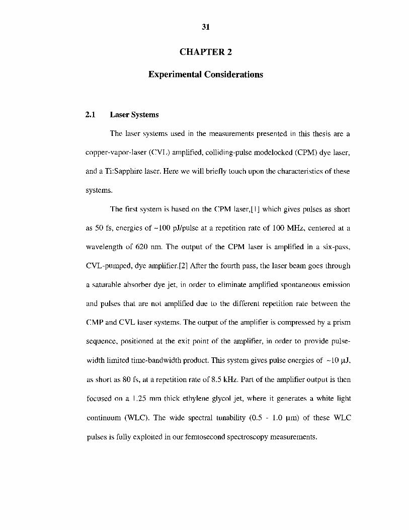
2.1 Laser Systems
The laser systems used in the measurements presented in this thesis are a
copper-vapor-laser (CVL) amplified, colliding-pulse modelocked (CPM) dye laser,
and a Ti:Sapphire laser. Here we will briefly touch upon the characteristics of these
systems.
The first system is based on the CPM laser,[l] which gives pulses as short
as 50 fs, energies of -100 pJIpulse at a repetition rate of 100 MHz, centered at a
wavelength of 620 nm. The output of the CPM laser is amplified in a six-pass,
CVL-pumped, dye amplifier.[2] After the fourth pass, the laser beam goes through
a saturable absorber dye jet, in order to eliminate amplified spontaneous emission
and pulses that are not amplified due to the different repetition rate between the
CMP and CVL laser systems. The output of the amplifier is compressed by a prism
sequence, positioned at the exit point of the amplifier, in order to provide pulse-
width limited time-bandwidth product. This system gives pulse energies of -10 pJ,
as short as 80 fs, at a repetition rate of 8.5 kHz. Part of the amplifier output is then
focused on a 1.25 rnrn thick ethylene glycol jet, where it generates a white light
continuum (WLC). The wide spectral tunability (0.5 - 1.0 pm) of these WLC
pulses is fully exploited in our femtosecond spectroscopy measurements.

The duration of the CVL pulse is -25 ns, and it is during this interval that
energy is stored in the amplifier dye. This is, therefore, the time span during which
the six passes of the CPM beam should take place. We need, therefore, a reliable
electronic circuit, in order to synchronize the CPM and the CVL lasers. The
synchronization electronics along with the laser system are shown in Figure 2.1.
Additionally, the CVL laser needs to be prevented from being turned off, if the
CPM laser is disturbed. The synchronization is accomplished by a gating
discriminator, in which the 100 MHz output from a photodiode detecting the CPM
pulses is gated by an 8.5 kHz, 15 ns, TTL signal. A digital delay is used to adjust
the triggering phase of the CVL, so that the six passes of the CPM beam coincide
with the peak of the CVL output pulse on the gain dye cell. Protection from shut-
down is accomplished by means of a coincidence unit, which is used to trigger the
CVL only when the CPM is off.
The Ti:Sapphire laser[3] is a folded cavity design, pumped by an "All lines"
Ar+ laser (Coherent Laser Group, model Innova 100). It produces 90 fs pulses at a
repetition rate of 85 MHz and with an energy of -10 nJ. An intracavity, two prism
sequence, provides the proper amount of group velocity dispersion for production
of transform limited pulses, and an adjustable slit is used to tune the central
wavelength of the light pulses from 800 nm to 900 nm. A schematic of the cavity is
shown in Figure 2.2.

-------------__-__ I I I CPM I
I "BAT" amplifier
22009
Figure 2.1 Schematic of the CVL-amplified CPM laser together with synchronization electronics. PD = photodiode, TA = timing amplifier, GD = gating descriminator, PG = pulse generator, DD = digit.al delay, CU = coincidence unit, BS = beam splitter.

All lines Ar-ion (13 W)
Figure 2.2 Schematic of the Ti:Sapphire laser cavity. OC = output coupler, MI, M2, M3, M4, and M5 = cavity mirrors, PI , P2 = prisms, S = tuning slit.

2.2 Sample Preparation
The thin film samples used in our measurements were grown by Solid
Source Molecular Beam Epitaxy (SSMBE) at The Institute of Optics of the
University of Rochester. The method used to remove the substrate differs,
depending on the epilayer, but all are based on a technique developed by
Yablonovitch et. al. for GaAs [5].
We will start our description of the sample preparation with the case of
GaAs. Two 0.3 pm thick layers of this material were prepared, at growth
temperatures of 250°C and 195°C. After growth, a piece of each was in situ
annealed at 600°C for 10 rnin. A 0.8 Fm thick layer of A10 gGa0 2As was stacked
between the epilayer and the substrate and served as a lift-off layer. A solution of
25 mg wax (Apiezon W) dissolved in 100 rnl of trichloroethylene was applied
uniformly on the epilayer side. After annealing at -100°C for < 112 h, the sides of
the sample were exposed, and the sample was stored in dilute (-20%) HF acid, at
0°C. At this high A1 concentration, HF etches the AlGaAs layer a few orders of
magnitude faster than it attacks GaAs. A selectivity of -107 has been measured
between AlAs and A10 4Ga0 AS, with the onset of etching occuring very suddenly
at about 40% to 50% A1 composition [5]. The annealing condition produces the
right amount of tension and curvature for the LT-GaAs film. The slight up-lifting
of the epilayer edges permits the resulting H2 gas to diffuse from the etching zone,
allowing the etching process to continue unimpaired. Typically, after -24 h in this
environment, the AlGaAs layer has been etched away completely, and the LT-
GaAs epilayer floats off. The layer, supported by the wax, is then carefully placed
on a sapphire window where it remains attached due to van der Waals forces. The
wax is then removed by submerging the whole structure in trichloroethylene for
five minutes. We have chosen sapphire instead of glass due to its excellent thermal
conductivity which minimizes thermal effects. The electronic quality of the
epitaxially grown films is unaffected by this lift-off process [5].
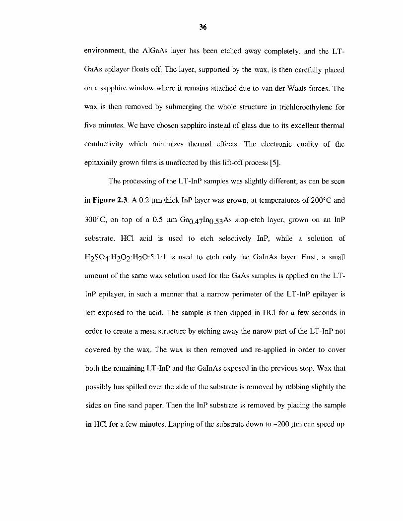
The processing of the LT-InP samples was slightly different, as can be seen
in Figure 2.3. A 0.2 pm thick InP layer was grown, at temperatures of 200°C and
300°C, on top of a 0.5 pm Gag 471110 53As stop-etch layer, grown on an InP
substrate. HC1 acid is used to etch selectively InP, while a solution of
H2S04:H202:H20:5:1:1 is used to etch only the GaInAs layer. First, a small
amount of the same wax solution used for the GaAs samples is applied on the LT-
InP epilayer, in such a manner that a narrow perimeter of the LT-InP epilayer is
left exposed to the acid. The sample is then dipped in HC1 for a few seconds in
order to create a mesa structure by etching away the narow part of the LT-InP not
covered by the wax. The wax is then removed and re-applied in order to cover
both the remaining LT-InP and the GaInAs exposed in the previous step. Wax that
possibly has spilled over the side of the substrate is removed by rubbing slightly the
sides on fine sand paper. Then the InP substrate is removed by placing the sanlple
in HC1 for a few minutes. Lapping of the substrate down to -200 pm can speed up
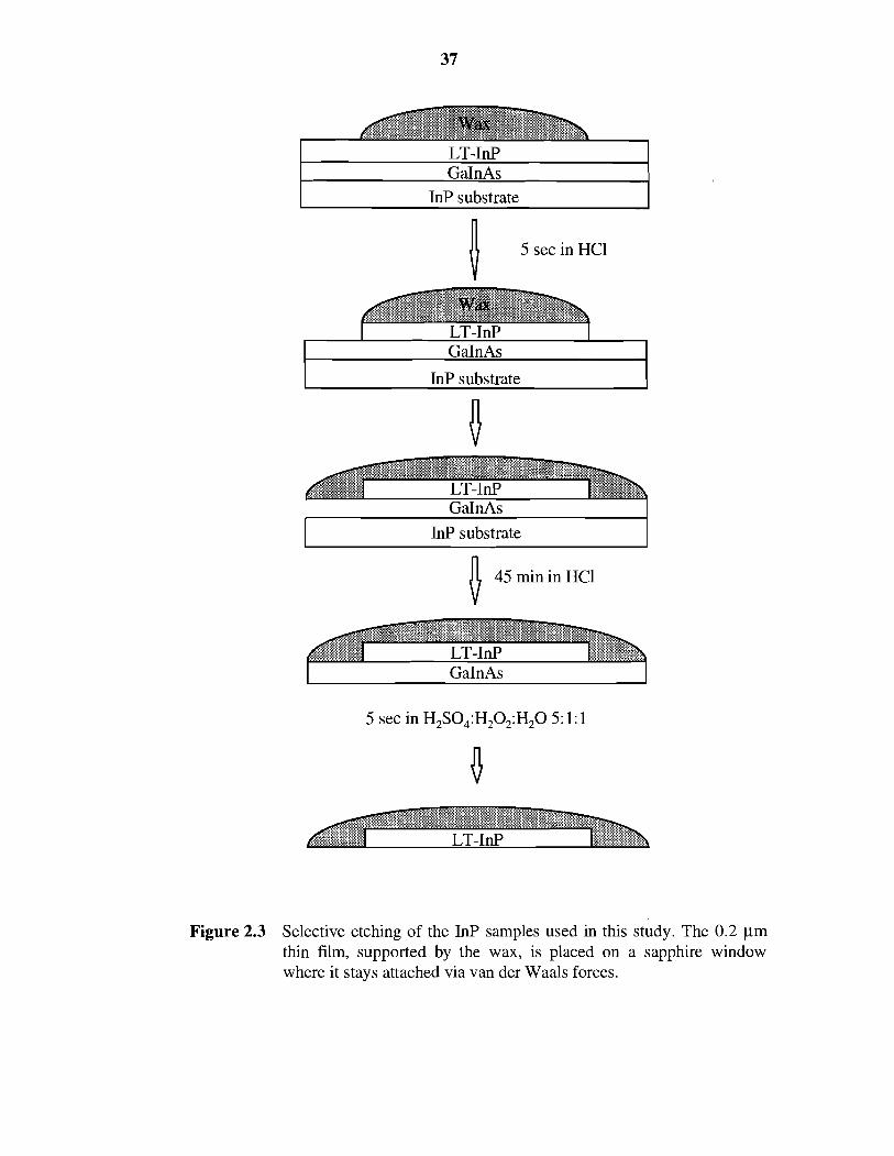
LT-InP GaInAs
InP substrate
0 5 sec in HCl
GaInAs
InP substrate
GaInAs
InP substrate
0 45 rnin in HCl
5 sec in H2S0,:H202:H20 5: 1: I
Figure 2.3 Selective etching of the InP samples used in this study. The 0.2 pm thin film, supported by the wax, is placed on a sapphire window where it stays attached via van der Waals forces.
this process. This is desired since a long exposure in the HC1 environment will
affect the LT-InP epilayer even if it is covererd by wax. This is evident by presence
of small holes in samples treated for -50 minutes and also by the appearance of
small air bubbles during etching of the substrate. Lapping the substrate down to an
even smaller thickness not only reduces etching time, but also makes the sample
difficult to handle. A subsequent dip for -10 sec in a H2S04:H202:H20:5: 1: 1
solution, completely etches the GaInAs layer, leaving only the LT-InP on the wax.
As in the GaAs case, the sample is van der Waals attached on a sapphire window.
A slightly different method was used in the case of Gag 5 lIno 4gP. The
epitaxial layers were directly grown on GaAs substrates, which were then lapped
down to -100 Lm thickness. After wax was applied on the epilayer, the samples
were placed in a solution of H2S04:H202:H20:5: 1: 1 at O°C, in order to etch
selectively the GaAs substrate at an etching rate of -8 pdhour. The 200°C, as-
grown and annealed, Ga051In049P samples, were prepared by using
NH40H:H202: 1:30 as a selective etch, reducing the processing time significantly.
2.3 Experimental Methods
Both the pump-probe and the up-conversion luminescence techniques are
used extensively to study the dynamics of excitations in a variety of materials and
physical systems. In this section we will give a brief description of both
experimental set-ups.
Illustrated in Figure 2.4 is the complete 2-eV-pump~WLC-probe
experimental arrangement. A simpler version of it has been used for the degenerate
pump-probe measurements with the Ti:Sapphire system. About 4% of the
amplified CPM pulse was split off as a 1100 fs pump pulse at 620 nm (-2 eV). The
remainder was used to generate a white light continuum in a flowing jet of ethylene
glycol, from which a wavelength tunable probe pulse was selected by means of
interference filters of 10 nm or 25 nm bandwidth. This allowed the probe
wavelength to be chosen in the range of 570 nm to 900 nm. Typical cross-
correlation measurements of the pump and probe pulses at 620 nm yielded widths
of 80 fs. When the probe is extracted from the WLC, it is usually slightly longer
by -15%-20%. Both pump and probe pulses are focused on the sample (at near
normal incidence) using the same lens. The polarization of the pump was rotated
by means of a half-wave plate to 90° with respect to that of the probe in order to
reduce coherent artifacts. The variable delay was achieved by diverting the pump
into a retroreflector mounted on a computer controlled, stepper-motor driven,
translation stage. The transmitted and reflected beams were collected
simultaneously by focusing lenses on two different photodiodes. Each of these
photodiodes was part of a subtraction scheme that made possible the measurement
of only the pump-induced changes in the transmission, AT, and reflection, AR, of
the sample and simultaneously was compensating for noise in the probe pulse train.
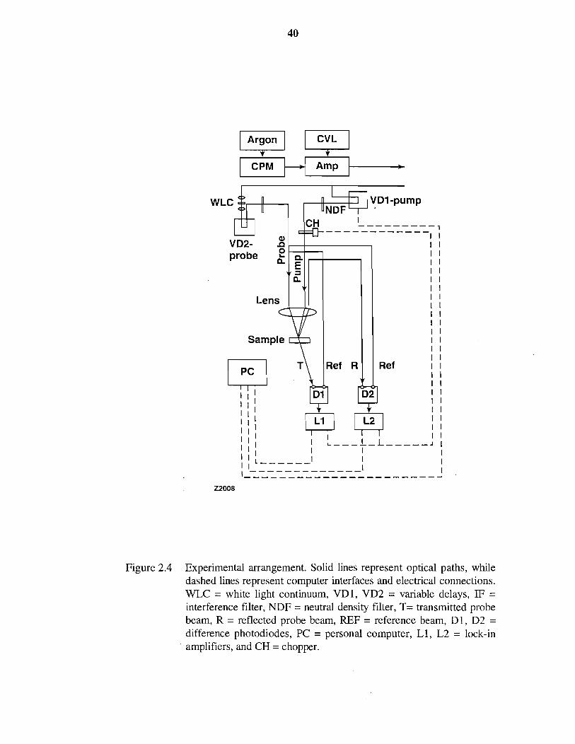
Figure 2.4 Experimental arrangement. Solid lines represent optical paths, while dashed lines represent computer interfaces and electrical connections. WLC = white light continuum, VD1, VD2 = variable delays, IF = interference filter, NDF = neutral density filter, T= transmitted probe beam, R = reflected probe beam, REF = reference beam, D l , D2 = difference photodiodes, PC = personal computer, L1, L2 = lock-in amplifiers, and CH = chopper.
The resulting AT and AR were induced in phase with the modulation of the pump
beam by an optical chopper, and were measured by two lock-in amplifiers. The
outputs of these amplifiers were read at each point of the variable time delay, and
averaged over many sweeps of the pre-determined time window. The control of
the two lock-in amplifiers, of the stepper motor, and the averaging of the raw data,
was implemented by a personal computer. The intensity of the pump pulse was
varied by up to three orders of magnitude, and the injected carrier density was
estimated from the energy per pulse, the absorption coefficient of the sample at the
pump wavelength, the measured focal spot size and the sample thickness. Typical
carrier densities range from 1017 cm-3 to 1019 ~ m - ~ . Due to the relatively low
repetition rate, it was difficult to achieve a good S/N ratio at lower carrier
densities, and in order to achieve carrier densities less than 1016 ~ m - ~ , we used the
unamplified CPM. Uncertainties in the beam parameters and/or in the absorption
coefficient of some of the samples, as well as the efficient surface recombination
on un-passivated samples [6], make the overall uncertainty of the absolute carrier
density about +50%.
Together with AT and AR, we also measure carefully To and Ro, the
undisturbed transmission and reflectivity, at each probe wavelength. With this
information at hand, we can determine T(T) and R(T) as a function of the time
delay z, from the relations: T(z)=To(l+AT/To) and R(T)=R~(I+AR/R,). The
samples used in this thesis are thin films on thick transparent substrates and show
clear Fabry-Perot fringes, especially when the probe wavelength is in the
transparency regime of the material. These fringes can obstruct the extraction of
physical information since both AT and AR can contribute to the observed signal.
In order to avoid this problems we transformed our data from T(T) and R(T) to
n(7) and k ( ~ ) , where n and k are the real and imaginary part of the index of
refraction, by reversing the Fabry-Perot formulas. The transmission T and
reflection R at normal incidence and at wavelength h, are given by [7 ] :
where

Here n and k are the real and imaginary parts of the refractive index of the film, d
is the thickness of the film, n l=l is the refractive index of air, and n3 is the
refractive index of the sapphire window which is given by [8]:
with h in units of Fm. Equations (1) and (2) are solved numerically, in order to
calculate the absorption coefficient a that is related to the imaginary part k of the
refractive index through: a=4nklh. Typical T and R traces are shown in Figure
2.5(a), while the calculated n and a are shown in Figure 2(b). Our system allowed
detection of changes as small as 10-5. The extraction of n and k from the
experimental values of T and R requires the use of initial guesses for the values of
no and ko, the unperturbed real and imaginary parts of the refractive index. These

1 2
Time (ps)
Figure 2.5 Measured reflection and transmission (a) and calculated index of refraction and absorption coefficient (b) using the Fabry-Perot formulas, of a LT-GaInP film grown at 200°C.

initial guesses are taken from the existing literature, and while they are well known
for GaAs [9] and InP [9], they are still under study in the case of GaInP [lo]. We
have found that the calculated values of n and k are sensitive to variations in these
initial guesses and also to uncertaintjes in the film thickness (mostly An).
The time resolved differential reflection has also been measured in bulk LT-
GaAs and LT-InP. The reflectivity at normal incidence is given by:
Then the change of the refractive index is related to the change in reflection by
2 2
- 4 . (n -k -1) 8 . n, . k, - " .An+
2 . Ak (no + I ) ~ + k, (n, + 1>2 + k
where no (ko) is the undisturbed real (imaginary) part of the refractive index of the
sample. This type of reflectivity measurements is mostly sensitive to probe
wavelengths near that of the pump, since probe light with penetration depth much
longer than that of the pump cannot detect the change effectively, due to the small
interaction length. For the pump, and consequently for the probe wavelengths used
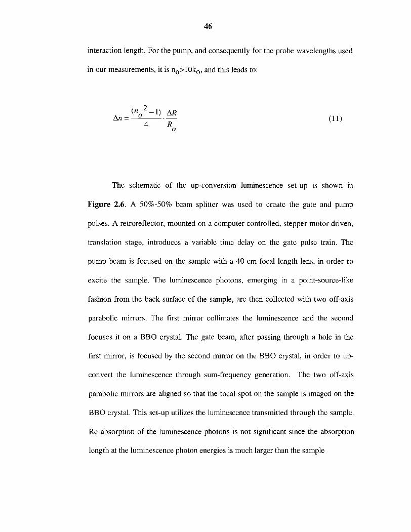
in our measurements, it is no>lOko, and this leads to:
The schematic of the up-conversion luminescence set-up is shown in
Figure 2.6. A 50%-50% beam splitter was used to create the gate and pump
pulses. A retroreflector, mounted on a computer controlled, stepper motor driven,
translation stage, introduces a variable time delay on the gate pulse train. The
pump beam is focused on the sample with a 40 cm focal length lens, in order to
excite the sample. The luminescence photons, emerging in a point-source-like
fashion from the back surface of the sample, are then collected with two off-axis
parabolic mirrors. The first mirror collimates the luminescence and the second
focuses it on a BBO crystal. The gate beam, after passing through a hole in the
first mirror, is focused by the second mirror on the BBO crystal, in order to up-
convert the luminescence through sum-frequency generation. The two off-axis
parabolic mirrors are aligned so that the focal spot on the sample is imaged on the
BBO crystal. This set-up utilizes the luminescence transmitted through the sample.
Re-absorption of the luminescence photons is not significant since the absorption
length at the luminescence photon energies is much larger than the sample
Monochromator
Figure 2.6 Schematic of the up-conversion luminescence set-up. BS = 50150 beam splitter, S = sample, BBO = P-Barium Borate, PMT = photomultiplier. The luminescence photons, together with the gate beam are up-converted in the BBO crystal. The resulting ultraviolet photons are then dispersed with the monochromator and counted with the PMT
thickness. The up-converted UV photons are then focused on the entrance slit of a
monochromator and detected using -photon-counting techniques. Both the rise time
and the decay time of the luminescence can be used to extract information about
the carrier dynamics.
References
J. A. Valdmanis, and R. L. Fork, IEEE J. Quantum Electron. QE-22, 112
(1986).
W. N. Nighan Jr., and P. M. Fauchet, Applications of Ultrafast Laser
Pulses in Science and Technology, SPIE Proc. 1268,79 (1990).
D. E. Spence, P. N. Kean, arid W. Sibbett, Opt. Lett. 16 ,42 (1991).
B. C. Tousley, Ph.D. Thesis, Department of Electrical Engineering,
Unniversity of Rochester, ( 1993).
E. Yablonovitch, T. Gmitter, J. P. Harrison, and R. Bhat, Appl. Phys. Lett.
51,2222 (1987).
J. F. Young, K. Wan, A. J. Springthorpe, and P. Mandeville, Phys. Rev. B
36, 13 16 (1987).
M. Born and E. Wolf, Principles of Optics, (Pergammon, Oxford, 1985) p.
630.
I. H. Malitson, J. Opt. Soc. Am. 52, 1377 (1967).
9. Handbook of the Optical Constants of Solids, ed. by E. D. Palik,
(Academic, London, 1985) p. 429.
10. M. Moser, R. Winterhoff, C. Geng, I. Queisser, F. Scholz, and A. Dornen,
Appl. Phys. Lett. 64, 235 (1994).

50
CHAPTER 3
Femtosecond Carrier Dynamics In Low Temperature-Grown
Indium Phosphide
3.1 Introduction
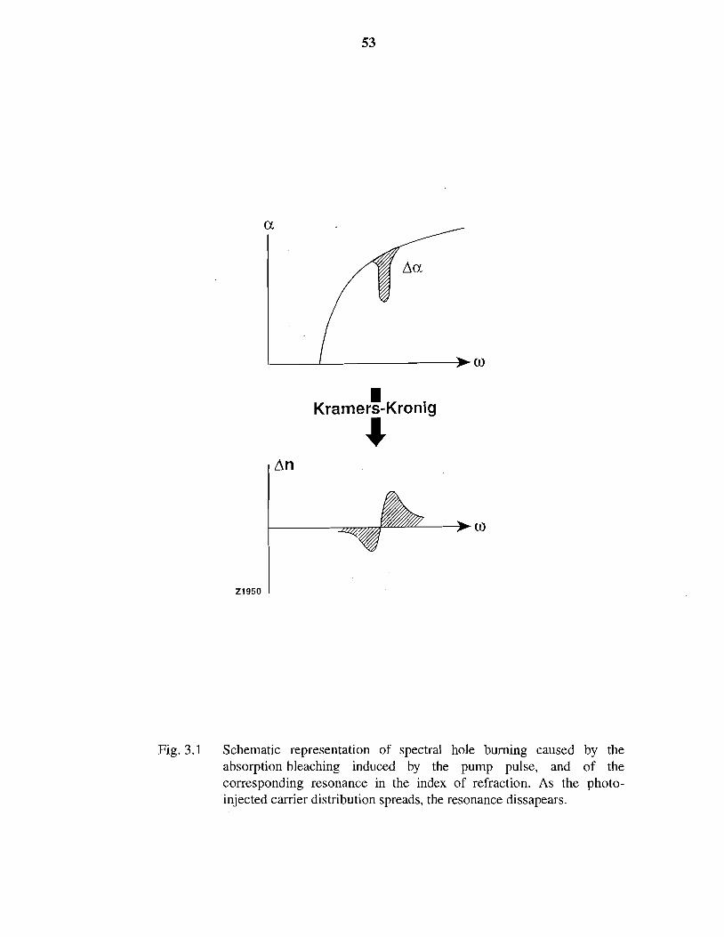
Electron and hole populatioris can be monitored through the band to band
absorption saturation. Before evolving toward a quasi-equilibrium, the electron-
hole distribution is expected to be peaked at the excitation energy, giving rise to a
dynamic spectral hole burning effect, i.e. a preferential bleaching at the excitation
energy. This absorption saturation is the result of filling of the states connected via
the excitation photons. As the as-excited carrier distribution thermalizes, the
carriers spread over a wide spectral distribution in the conduction band and the
spectral hole disappears.
With the advent of the femtosecond lasers, it has been possible to observe
in real time the spectral hole burning associated with the absorption saturation of
valence-to-conduction band transitions. The absorption spectral hole burning was
first directly observed near the band edge of bulk GaAs by Oudar [ I ] and also later
by Hunsche [2] and in intrinsic ancl doped quantum wells by Knox [3,4] and its
recovery was used to deduce the dwell times of the carriers in the as-excited states.
Later such hole burning was observed for excitation high (-2 eV) in the
conduction band of GaAs by pump and continuum-probe measurements [5-71.
When the Kramers-Kronig relations are applied, a dynamic spectral hole burned in
the absorption spectrum gives rise to a spectral resonance in the index of refraction
[S]. Changes in the index of refractjon are readily observable in an optically thick
sample for which AR-An (see chapter 2 page 52) and information about refractive
nonlinearities and carrier dynamics c.an be extracted.
If pump and probe measurements are performed at the same wavelength,
the recovery of the bleaching yields information on the dwell time of the carriers in
the as-excited states. Both equal-pulse correlation and non-linear pump-probe
techniques have been used to measure the time it takes for carriers to scatter out of
the initially excited states. When the excitation takes place high in the conduction
band and states close to the band edge are probed, the rise time of the signal also
contains information about the carrier cooling [9,10]. When pump-probe
spectroscopy is used to study the carrier trapping time or lifetime, complications
arise from carrier relaxation which can contribute significantly to the observed
signal decay.
The decay of the band edge luminescence, on the other hand, can provide
transparent information about the carrier trapping time or lifetime.
In this chapter we use these two complementary methods to study the
dynamics of photoexcited carriers in low-temperature grown InP. By contrasting
the results from the two methods we find that carrier trapping and not
recombination is the ultrafast effect :in this material.
52
3.2 Refractive Index Spectral Hole Burning
For a conventionally grown III-V semiconductor, the pump pulse at t - 0+
causes a sharp reduction of the absorption at the pump wavelength due to state
filling. By means of the Krarners - Kronig relations this dynamic bleaching will
cause a spectral resonance in the index of refraction. For an optically thick
semiconductor (thickness >> absorption length at the pump photon energy), a
change in reflectivity is proportional to a change in the index of refraction and the
above mentioned resonance should therefore be evident in the reflectivity data. The
manifestation of such a spectral resonance is a short-lived negative dip at z - 0+
for probe photon energies smaller than the pump. At the zero point of the spectral
resonance, which takes place when hprobe = hpump, we expect no spectral
features at t - O+. When the probe photon energy becomes larger than that of the
pump, we probe the positive part of the spectral resonance and we would
anticipate a short-lived positive feature to appear in the reflectivity right after
carrier injection. This can be see.n in Figure 3.1 where a schematic of the
absorption and refractive index spectral hole burning is depicted.
Figure 3.2 shows the time resolved differential reflection of an intrinsic
bulk GaAs sample grown at normal temperatures measured using the CPMJCVL
laser system (T. Gong, Ph.D. Thesis [ l l ]) . The probe wavelength varies from 600
nm to 700 nrn and the injected carrier density is 2-3x10~8 ~ m - ~ . The data at 600
nm and 620 nm exhibit a short-lived positive spike right after carrier injection,
I Kramers-Kronig
Fig. 3.1 Schematic representation of spectral hole burning caused by the absorption bleaching induced by the pump pulse, and of the corresponding resonance in the index of refraction. As the photo- injected carrier distribution spreads, the resonance dissapears.

whereas the data at 680 nm and 700 nm exhibit a negative spike. No fast feature is
observed at a probe wavelength of 650 nm. These positive and negative spectral
features observed right after carrier injection are a clear demonstration of the
refractive index spectral hole burning. In reflectivity measurements, the probe
wavelength cannot be varied much compared to that of the pump since the
penetration depth increases or decreases quicldy leading to a small overlap and
consequently to a small interaction length in the sample. The relatively large width
of the spectral hole (-200 meV) indicates that carrier-carrier scattering has
redistributed electrons in the r valley within the pulse width. In addition, the zero
point of the spectral resonance appears to be at 650 nm instead of the pump
wavelength of 620 nm. This peculiarity is due to the influence of intervalley
scattering which leads to an apparent accumulation of carriers in the r valley at an
energy -30 meV below the X-valley minimum, causing the peak of the spectral
resonance to appear at -650 nm [12].
After -200 fs, the resonance disappears because carriers leave the initial
excited Bloch states by various scattering processes. The similar gradual rise of An
on a picosecond time scale in the 600 nm - 700 nm spectral range is due to band
filling which is controlled in part by the slow return of carriers from the L valley.
Having the GaAs differential reflectivity measurements as a benchmark, we
proceed to investigate the behavior of bulk InP grown at normal temperatures
under the same experimental conditions. The corresponding data for an injected
carrier density of 8x1018 cm-3 are depicted in Figure 3.3. Again the spectral

Fig. 3.2 Transient spectral hole burning: as the probe wavelength varies around 2 eV, we clearly see t:he positive and negative part of the spectral resonance at z -0+ for conventionally grown GaAs [after T. Gong, Ph.D Thesis, Princeton TJniversity 1991).

h V) C, .- s 3
5 (El L C, ..I
0 L (El V
A C, ..I > ..I
C, 0 Q) I - Q) a
0.0 1.0 2.0 3.0
Time (ps)
Fig. 3.3 Transient spectral hole burning in the case of conventionally grown InP substrate (comp. Figure 3.2). The high injected carrier density (-1019 cm-3) leads to a significant spread of the carrier distribution within the pulse width. This prevents the resolution of the falling edge of the 590 nm signal at z -O+ fs.
resonance is clearly visible. The band structure of InP is different than that of
GaAs. The X and L valley minima are at higher energies than in GaAs and
therefore, no significant intervalley transfer can take place. As a result, the zero of
the spectral resonance is at the pump wavelength of 620 nm. At the smaller probe
photon energies the negative part of the spectral resonance is clearly visible. As the
photon energy is increased above that of the pump, only the rise time of the
resonance can be resolved as can be seen from the much faster rise of the signal at
590 nm compared to that at 620 nm. The reason for that is the fast thermalization
through carrier-carrier scattering at these high injected carrier densities. This leads
to an appreciable spread of the injected carrier distribution within the probe pulse
width. As the excited carriers undergo fast relaxation, the positive contribution of
bandfilling [13] to the index of refraction becomes prominent. The negative part of
the spectral resonance is not affected by this change of sign. The positive part of
the spectral resonance on the other hand, is overwelmed by the contribution of
bandfilling which obstructs the resolution of its falling edge.
The same measurements are performed on a 5 km thick LT-InP layer
grown at 200°C, and can be seen in Figure 3.4. This sample is polycrystalline and
has -7% excess phosphorus due to the growth at low substrate temperatures [14].
Under the same experimental conditions the LT-InP sample exhibits a totally
different behavior. As the probe wavelength is varied we observe no transient
spectral hole burning: the change in reflectivity right after carrier injection is
always negative. For all probe wavelengths the signal recovers on a fast time scale
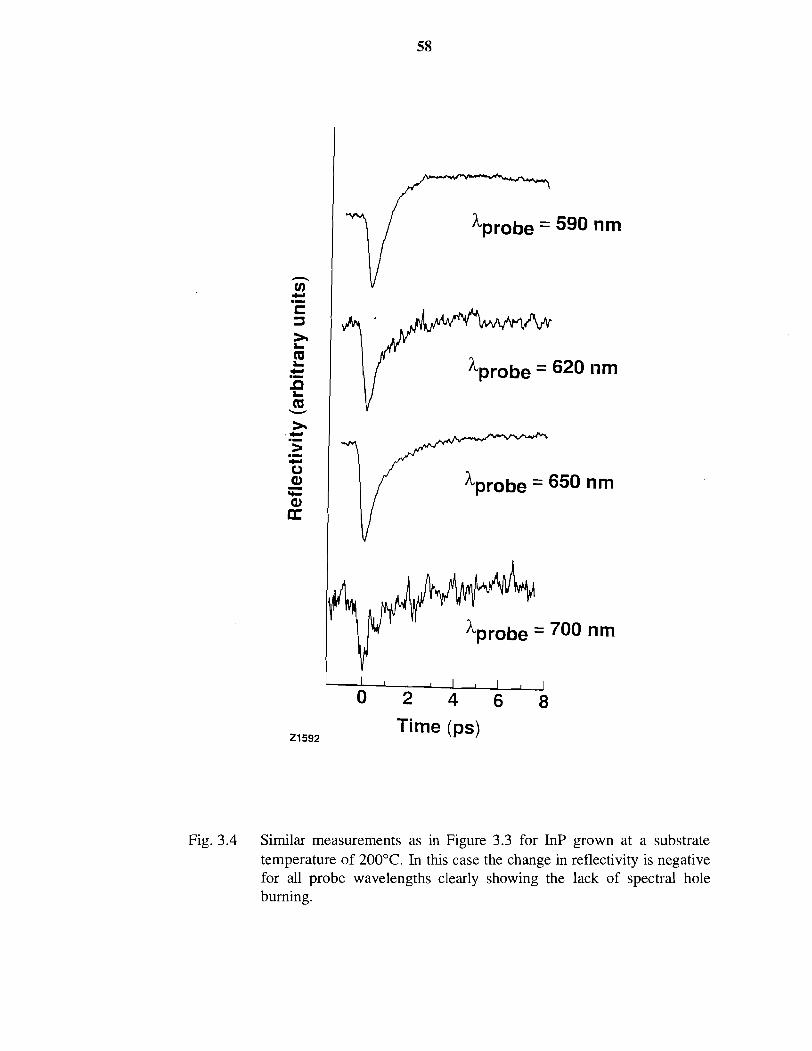
0 2 4 6 8
Time (ps)
Fig. 3.4 Similar measurements as in Figure 3.3 for InP grown at a substrate temperature of 200°C. In this case the change in reflectivity is negative for all probe wavelengths clearly showing the lack of spectral hole burning.
(-1 ps) and reaches a positive plateau. A similar behavior has been observed at 2
eV by Gupta etal. [15] in single crystalline LT-GaAs grown at 200°C. This
negative change in reflectivity for all probe wavelengths is a characteristic
signature of free carrier absorption,, but this is not compatible with transmission
experiments on LT-InP films as we ,will see below. The existence of a defect band
in the LT-material which affects our data through the integration over all energies
in the Kramers-Krijnig relations complicates the interpretation of the reflectivity
measurements.
3.3 Carrier Trapping vs Carrier Recombination
In order to avoid the complications introduced by the Kramers-Krijnig
relations and to investigate more thoroughly the carrier trappinglrecombination
lifetimes in LT-InP, we performed. up-conversion luminescence experiments in
conjunction with 2 - e V- pu mpl WLC - pr o be differential transmission
measurements, on two LT-InP thin films grown at 200°C and 300°C. No annealing
was performed and X-ray diffraction measurements show both samples to be of
good crystalline quality. Their thickness was 0.2 Fm which is approximately equal
to one absorption length for the 12 eV pump photons, ensuring fairly uniform
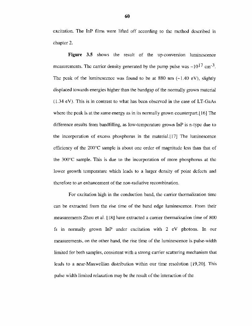
excitation. The InP films were lifted off according to the method described in
chapter 2.
Figure 3.5 shows the result of the up-conversion luminescence
measurements. The carrier density generated by the pump pulse was -1017 cm-3.
The peak of the luminescence was found to be at 880 nrn (-1.40 eV), slightly
displaced towards energies higher than the bandgap of the normally grown material
(1.34 eV). This is in contrast to what has been observed in the case of LT-GaAs
where the peak is at the same energy as in its normally grown counterpart.[l6] The
difference results from bandfilling, as low-temperature grown InP is n-type due to
the incorporation of excess phosphorus in the material.[l7] The luminescence
efficiency of the 200°C sample is about one order of magnitude less than that of
the 300°C sample. This is due to .the incorporation of more phosphorus at the
lower growth temperature which leads to a larger density of point defects and
therefore to an enhancement of the n.on-radiative recombination.
For excitation high in the conduction band, the carrier thermalization time
can be extracted from the rise time of the band edge luminescence. From their
measurements Zhou et al. [18] have extracted a carrier thermalization time of 800
fs in normally grown InP unde.r excitation with 2 eV photons. In our
measurements, on the other hand, the rise time of the luminescence is pulse-width
limited for both samples, consistent .with a strong carrier scattering mechanism that
leads to a near-Maxwellian distribution within our time resolution [19,20]. This
pulse width limited relaxation may be the result of the interaction of the
Time (ps)
Fig. 3.5 Up-conversion photoluminescence traces of (a) the 300°C sample and (b) the 200°C sample. The signal is measured at the peak of the photoluminescence. The pulse width limited rise time indicates a carrier distribution that extends to the bottom of the conduction band within our time resolution.
photoexcited carrier distribution with a cold Ferrni sea of electrons of higher
density already present in the conduction band. (An extremely fast initial scattering
time of -25 fs has been observed in 11-type GaAs arising from the coupled phonon-
plasmon modes) [20]. The fact that a pulse width limited thermalization has also
been observed in other LT-IIINs that are of high resistivity, indicates that other
scattering mechanisms, such as defect ionization scattering can also contribute to
this effect. The relaxation of carriers to the band edge within the pump pulsewidth
shows that in the thin film samples, as in the polycrystalline sample, no spectral
hole is observed.
The up-conversion luminescence signal decays exponentially with a time
constant (without deconvolution) of 0.45 ps for the 200°C sample and 1.6 ps for
the 300°C sample. These time constants are due to carrier trapping and not
recombination, as will be seen from the pump-probe measurements. A similar
carrier trapping time has also been observed in the case of GaAs grown at 200°C
[16].
The differential transmission measurements are shown in Figure 3.6. The
carrier density generated by the pump pulse was - 1 0 ~ 9 cm-3 for these
measurements. We observe a pulse-width limited rise time of the bleaching signal
for both samples, at all probe wavelengths from 570 to 860 nm. The photo-
excitation of a nearly monoenergetic electron distribution in the conduction band
of conventionally grown GaAs using 2 eV photons induces a bleaching signal with
a slow rise at probe wavelengths close to the band edge [20,2:1]. This effect is

- 3 (PS) - Time
Fig. 3.6 Differential transmissiorl measurements on the same samples as in Figure 3.5. The fast decay of the bleaching is due to carrier trapping with the recombination tiking place in a much longer time scale.
caused by the cooling of the photo-generated carriers down to states near the
bottom of the conduction band. Such behavior is not observed in low temperature
grown InP, indicating that the carrier distribution broadens significantly within our
time resolution. This wavelength-independent, pulsewidth limited rise time is
consistent with what we observe from the luminescence measurements and
confirms that the carrier distribution extends to the bottom of the conduction band
in a time less than the excitation pulse.
In the case of the 200°C sample, the recovery of the signal is qualitatively
similar for all probe wavelengths. The bi-exponential decay has a fast component
of -150 fs and a slower component of -650 fs. A bi-exponential decay of the
bleaching signal is also observed in the case of the 300°C sample but the amplitude
of the fast component becomes smaller at longer probe wavelengths and the slower
time constant is longer, -2 ps. Trap saturation largely contributes to these longer
time constants, as will be seen below. The fast component is attributed to cooling
of the photo-excited carriers in the conduction band while the slower component,
which is close to the time constant observed in the up-conversion luminescence
measurements, describes carrier trapping. The fast decay of the signal is partly the
result of electron-electron interactions between a cold Fermi sea and the hot
distribution of photo-excited carriers, which results an efficient channel for carrier
relaxation [20,22]. This can be seen also in Figure 3.7, where we plot the 620-620
nrn pump-probe trace at three injected carrier densities differing by more than an
order of magnitude. The initial decay of the bleaching is faster at lower injected

Fig. 3.7 Differential transmission measurements on the 200°C sample at 620 nm and three injected carrier densities: The initial decay of the bleaching becomes faster as the carrier density is decreased. The traces are normalized with respect to their peaks for comparison.

carrier densities since the number of' photo-injected hot electrons interacting with
the cold Fermi sea at the bottom of the conduction band is smaller, resulting in a
faster temperature equilibration. We note that intervalley scattering does not
contribute significantly to the fast recovery of the signal in the case of InP, since 2
eV photons excite electrons in the conduction band with an excess energy below
the intervalley scattering threshold.
In an attempt to deduce the contribution of carrier-carrier scattering to the
fast carrier relaxation observed in our experiments, we performed differential
transmission measurements at 2 e'V on a normally grown InP film which was
intentionally n-type doped to N ~ = ~ X I O ~ ~ ~ m - ~ . The results are contrasted with
those of the 200°C sample in Figure 3.8. Both traces are taken under similar
injected carrier densities (-1019 cm-3) and are normalized to their peak values for
comparison. Even though both samples have a similar density of residual electrons
in their conduction bands, their response at 2 eV is markedly different. A small
partial relaxation is observed right after photo-excitation in the n-type InP sample,
followed by a slow recovery due to bandfilling. A small increase of the
transmission observed at longer time delays is probably due to the return of
carriers from the satellite valleys. Even though in InP carriers injected with 2 eV
do not have enough excess energy for intervalley scattering, at high injected carrier
densities, electron-electron scattering causes the tail of the carrier distribution to
extends to energies high enough for intervalley transfer. In the 200°C grown
sample, on the other hand, the initial carrier relaxation is of much larger amplitude.
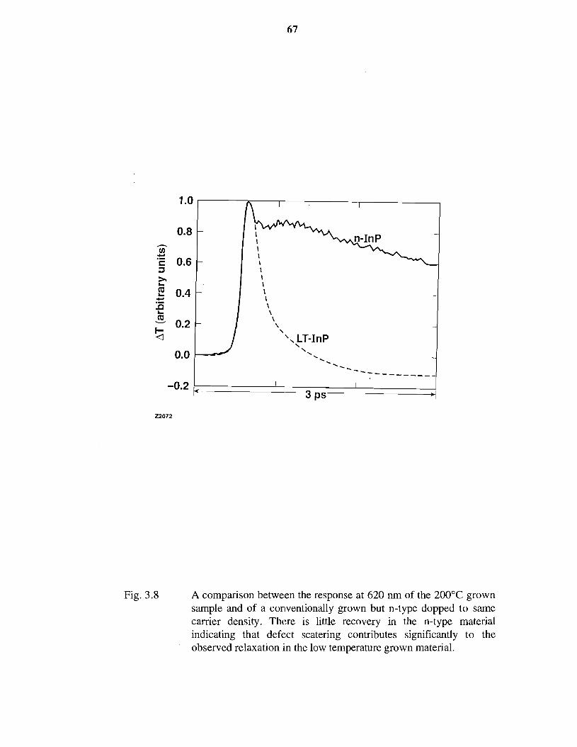
Fig. 3.8 A comparison between the response at 620 nrn of the 200°C grown sample and of a conventionally grown but n-type dopped to same carrier density. There is little recovery in the n-type material indicating that defect scatering contributes significantly to the observed relaxation in the low temperature grown material.
These differences indicate that other scattering mechanisms such as ionized
impurity scattering contribute significantly to the fast relaxation observed in the In
the sample grown at 200°C, the bleaching observed immediately after photo-
injection turns into induced absorption (i.e. negative transmission plateau) after 1
ps. This plateau does not decay for tens of picoseconds and has also been observed
in femtosecond transmission spectroscopy measurements close to the band gap of
GaAs as-grown at 250°C [23].
Even if we assume that the energy of each photon absorbed during the
excitation process is transferred to the lattice through multi-phonon, non-radiative
recombination, the change in the optical properties of the material due to lattice
heating cannot account for the observed induced absorption. For a photo-excited
carrier density of n-1019 cm-3, a pump photon energy of 2 eV and taking the heat
-1 -1 capacity of InP at 298 K to be 0.32. J g K [24], we find a lattice temperature
increase of AT -2 K if all carriers recombine non-radiatively. Since the bandgap
energy depends on temperature as E ~ ( T ) = E ~ ( o ) - ~ T ~ / ( T + ~ ) with Eg(0)=l .421 eV,
a=3.63 eV/K and b=162 K [25], an increase in the lattice temperature by -2
K, will cause an increase of the absorption coefficient by -30 cm-l. A lattice
temperature increase by -2 K is an overestimate, since it assumes that all photo-
excited carriers recombine non-radiatively. Therefore the actual induced
absorption due to lattice heating is expected to be even smaller than 30 cm-l. This
can not explain our experimental results which at 620 nm and at an injected carrier
of - 1019 cm-3 show an increase jn absorption by a factor of -1000 cm-l. We
conclude that the large induced absorption plateau is caused by re-absorption of
the probe photons by the carriers trapped in the defects. From the magnitude of the
induced absorption we can estimate the absorption cross section: with Aa -1000
cm- l and for n- 10 ~ m - ~ , we find o = A d n - 10- cm2. Even though the nature
of these traps is not known at present, their photo-ionization cross-section is
similar to that of the EL2 defect in GaAs [26]. We conclude that the photo-excited
carriers are first undergoing a fast trapping process, with recombination following
at a longer time scale (>> 10 ps). The decay constant of the luminescence signal,
therefore, describes the trapping time and not the lifetime of the photo-excited
carriers. The fast carrier lifetime observed in LT-grown GaAs [23] and LT-grown
InGaAs [27] may also be interpreted in the same way.
The induced absorption plateau is also observed in the case of the 300°C
sample but at longer time delays. This is due to the saturation of the traps at the
high injected carrier densities used in our pump-probe measurements. In Figure
3.9 we compare the change in transmission at 620 nrn in the 200°C and 300°C
samples, at injected carrier densities of -1016 ~ m - ~ , i.e. three orders of magnitude
smaller than the 2-eV-pump/WLC.-probe measurements depicted in figure 3.6.
After normalizing both traces to their peak values for comparison, we see that the
signal recovers in both samples at the same rate. In other words, when the injected
carrier density is lower than the density of point defects in both samples, their
behavior is identical. The decay of the bleaching in the sample grown at 200°C
changes only slightly as the injected carrier density is increased from 1016 cm-3 to

Fig. 3.9 Saturation of the traps at high injected carrier densities is evident when the recovery of the bleaching at 620 nm is found to be identical for both the 200°C and the 300°C samples at Nhj - 1o16 cm-3.
1019 cm-3 indicating that the density of the traps is t 1019 in this sample. In
the sample grown at 300°C, on the other hand, a similar estimate leads to a trap
density of mid- 1017 cm-3.
In conclusion, we have presented the results of differential reflection,
transmission, and up-conversion luminescence measurements on optically thick and
thin LT-InP films grown at 200°C and 300°C. Even though the electronic and
structural properties of this material differ appreciably from those of LT-grown
GaAs, the optical response is very similar.
No spectral hole is observed in the reflectivity measurements within our
time resolution. This is consistent with the pulse width limited rise time of the band
edge luminescence and of the band edge photo-induced bleaching measurements.
Trapping of photoexcited carriers takes place in a subpicosecond time scale
with time constants of 0.45 ps for the 200°C sample and 1.6 ps for the 300°C
sample. Carrier recombination takes place on a much longer time scale. A strong
scattering mechanism appears to dominate the carrier dynamics in the first 100 fs
after photo-excitation. This relaxation is mostly due to mechanisms such as defect
ionization scattering as can be seen from a comparison with an n-type film, grown
at high (-500°C) temperature.
Re-absorption of the probe photons by the trapped carriers leads to
induced absorption at time delays greater than -1 ps. The trap photo-ionization
cross-section is -10-l6 cm2 at 2 eV. Saturation of the traps is observed at high

injected carrier densities, leading to a slower recovery of the bleaching for samples
grown at the higher substrate temperatures.
References
1. J. L. Oudar, D. Hulin, A. Migus, A. Antonetti, and F. Alexandre, Phys.
Rev. Lett. 55, 2074 (1985).
2. S. Hunsche, H. Heesel, A. Ewertz, H. Kurtz, and J. H. Collet, Phys. Rev. B
48, 17818 (1993).
3. W. H. Knox, D. S. Chemla, G. Livescu, L. E. Cunningham, and J. E.
Henry, Phys. Rev. Lett. 61, 1 290 (1 988).
4. W. H. Knox, C. Hirlimann, D. A. B. Miller, J. Shah, D. S. Chemla, and C.
V. Chang, Phys. Rev. Lett. 56, 1191 (1986).
5. C. H. Brito-Cruz, R. L. Fork, and C. V. Shank, IQEC Technical Digest, p.
82 (1987).
6. R. W. Schoenlein, W. Z. Lin, E. P. Ippen, and J. G. Fujimoto, Appl. Phys.
Lett. 51, 1442, (1987).
7. W. Z. Lin, R. W. Schoenlein, J. G. Fujimoto, and E. P. Ippen, IEEE J.
Quantum Electron. QE-24,267 (1988).
8. D. C. Hutchings, M. Sheik-Bahae, D. J. Hagan, and E. W. Van Stryland,
Opt. Quantum Electron. 24, 1 (199 1).

J. Shah, B. Deveaud, T. C. Damen, W. T. Tsang, A. C. Gossard, and P.
Lugli, Phys. Rev. Lett. 59, 2222 (1987).
J. N. Sweetser, T. J. Duhn, I,. Waxer, I. A. Walmsley, S. M. Shank and G.
W. Wicks, Appl. Phys. Lett. 63, 3461, (1993).
T. Gong, "Femtosecond Nonlinearities And Hot Carrier Dynamics In
GaAs", Ph. D. Thesis Princeton University, (1991).
J. -Y. Bigot, M. T. Portella, R. W. Schoenlein, J. E. Cuningham, C. V.
Shank, Phys. Rev. Lett. 65, 3429 (1990).
B. R. Bennett, R. A. Soref, and J. A. Del Alamo, IEEE J. Quantum
Electron. QE-26, 1 13 (1 990:).
K. Xie, C. R. Wie and G. W. Wicks, Mat. Res. Soc. Symp. Proc. 241, 265
(1992).
S. Gupta, J. F. Whitaker, and G. A. Mourou, IEEE J. Quantum Electron.
QE-28,2464 (1 992).
X. Q. Zhou, H. M. van Driel, W. W. Riihle, Z. Gogolak, and K. Ploog,
Appl. Phys. Lett. 61, 3020 (1992).
P. Dreszer, W. M. Chen, K. Seendripu, J. A. Wolk, W. Walukiewitz, B. W.
Liang, C. W. Tu, and E. R. Weber, Phys. Rev. B. 47,4111, (1993).
X. Q. Zhou, G. C. Cho, U. L,emmer, W. Kiitt, K. Volter, and H. Kurz, Sol.
State Electron. 32, 159 1 (1989).
A very fast luminescence rise time could also arise from recombination of
electrons from the large cold electron reservoir with the photogenerated
holes. The pump-probe measurements shown in Fig. 2, however, support
the interpretation in the text.
T. Gong, P. Mertz, W. L. Nighan Jr., and P. M. Fauchet, Appl. Phys. Lett.
59,721-723 (1991).
T. Gong, W. L. Nighan Jr. and P. M. Fauchet, Appl. Phys. Lett. 57, 2713,
(1990).
T. Gong, P. M. Fauchet, J. F. Young, and P. J. Kelly, Phys. Rev. B 44,
6542 (1991).
E. S. Harmon, M. R. Melloch, J. M. Woodall, D. D. Nolte, N. Otsuka, and
C. L. Chang, Appl. Phys. Lett. 63,2248 (1993).
U. Piesbergen, "Semiconductors and Semimetals," in Physics of 111-V
Compounds, edited by R. K. Willardson and A. C. Beer (Academic Press,
NY, 1966), Vol. 2, p. 52.
"Properties of Indium Phosphide," EMIS Datareviews Series, Vol. 6,
(INSPEC Institution of Elect.rica1 Engineers , London, 199 1).
G. C. Valley, T. F. Boggess, J. Dubard, and A. L. Srnirl, "Picosecond
Pump-Probe Techniques to Measure Deep-Level, Free-Carrier, and Two
Photon Cross Sections in GaAs," J. Appl. Phys. 66, 2407 (1989).
B. C. Tousley, S. M. Mehta, A. I. Lobad, P. J. Rodney, P. M. Fauchet, and
P. Cooke, "Femtosecond Optical Response of Low Temperature Grown
In0 53Ga0 47As," J. Electron. Mater. 22, 1477 (1 993).
CHAPTER 4
Femtosecond Carrier Dynamics In Low Temperature-Grown
Ga0.5 1In0.49P
4.1 Introduction
The success of LT-GaAs in a variety of applications has prompted the
study not only of other As-based, low temperature grown 111-V compounds, but
also of the P-based materials. In the previous chapter we discussed the results of
pump-probe and up-conversion luminescence spectroscopy on LT-InP. The optical
response of this material is similar to that of LT-GaAs, even though their electrical
properties are quite different. We have seen that InP when grown at low
temperatures (-200°C) is heavily n-type due to the donor nature of the PI, antisite
defect, which has an energy level degenerate with the conduction band. This does
not change even after annealing at high temperatures.
Another phosphorus based material of technological importance is the
ternary Gag 511110 4 9 P It is lattice matched to GaAs and thus epitaxial layers
made of this material are compatible with the relatively mature GaAs technology.
With both n- and p-type doping available and a relatively wide band gap of 1.9 eV,
many device applications have been proposed and are implemented. For example, a
high valence band discontinuity w:ith GaAs and a low Be diffusion coefficient,
make GaInP an attractive material for GaInPIGaAslGaAs heterojunction bipolar
transistors [I]. However, a common problem in many semiconductor materials is
the lack of a stable, semi-insulating form. In the case of GaInP, growth at low
substrate temperatures can solve this problem effectively.
When as-grown between 150°C and 250°C, low-temperature
Gag 5 1Ino 49P (LT-GaInP) is weakly n-type with a room temperature resistivity
of -9x10⁵ Qcm, a mobility of 120 c m 2 ~ s , and a donor activation energy of 0.48
e ~ . ~ The lattice constant is increased by 0.05%, which corresponds to a -47% In
content.[3] After annealing at 600°C for 1 hour, the resistivity increases to lo9
Qcm and the activation energy to 0.8 eV.[2,3] These properties, if accompanied by
a short carrier trapping time, make LT-GaInP an attractive candidate for fast
photoconductive switch and metal-insulator field-effect (MISFET) transistor
applications. In this chapter we show that the carrier trapping time in this material
is <1 ps, depending on the growth temperature and the annealing conditions, and
that the point defects caused by the low temperature growth are directly
responsible for this ultrafast response.
We make use of the 2-eV-pump/WLC-probe system in order to investigate
carrier dynamics in samples grown at 500°C, 300°C, and 200°C. Due to the
proximity of the band gap luminescence to the pump photon energy, it is
impossible to perform up-conversion luminescence measurements with this system.
The noise introduced from the doubled pump photons obscures the low level
photon counting of the band gap luminescence.
77
4.2 Carrier Dynamics in High Temperature Grown GaInP
In order to investigate properly the dynamics of carriers in LT-grown
GaInP, we first attempt a characterization of the material grown at normal
substrate temperatures of -500°C. In Table I we summarize the material
parameters for GaInP. The corresponding values of GaAs are quoted for
comparison.
The sample that was used in this study was grown by gas source molecular
beam epitaxy (GSMBE) at a substrate temperatures of 500°C. X-ray diffraction
measurements showed good crystalline quality. The thickness was 0.5 pm, which
is approximately equal to one absorption length for 2 eV photons. The GaAs
substrates were selectively etched (see chapter 2), and the epitaxial layers were
attached to sapphire windows using van der Waals forces. In order to verify that
the substrate was completely removed after the etching process, we performed CW
luminescence measurements exciting the sample with the 514 nm Ar+ laser line.
This measurement was also used to determine the band gap of the epitaxial layer.
The results are shown in Figure 4.1. There is no evidence of the GaAs substrate in
the CW luminescence trace and the band gap energy of the GaInP layer is found to
be 1.89 eV at room temperature. In all the experiments reported here, the
excitation energy is 2 eV. From the material parameters of Table I we calculate the
carrier kinetic energies to be: &,hh = 89 meV , &Lh = 68 meV , for the
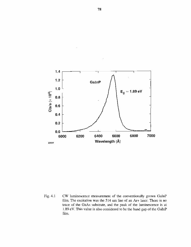
6000 6200 6400 6600 6800 7000
22032 Wavelength (A)
Fig. 4.1 CW luminescence measurement of the conventionally grown GaInP film. The excitation was the 514 nm line of an Ar+ laser. There is no trace of the GaAs substrate, and the peak of the luminescence is at 1.89 eV. This value is also considered to be the band gap of the GaInP fh.
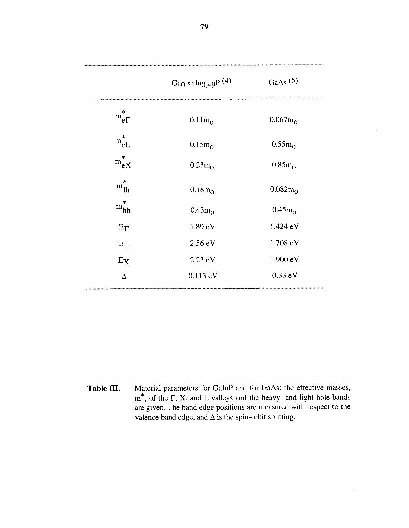
Ga0.5 1 ~ ~ 0 . 4 9 ~ (4) GaAs (5)
Table 111. Material parameters for GaInP and for GaAs: the effective masses, * m , of the r, X, and L valleys and the heavy- and light-hole bands are given. The band e,dge positions are measured with respect to the valence band edge, and A is the spin-orbit splitting.
electrons from the heavy and light holes, and ehh = 22 meV, and
~ l h = 42 meV for the heavy and light holes respectively. With a value of A=O. 11
eV, excitation of carriers from the spin-split off band at the bottom of
theconduction band is also allowed. The vanishing density of states though,
renders the effect of this transition negligible. The satellite valleys are at much
higher energies, as can be seen from Table I, so that for 2 eV photon excitation we
can ignore intervalley scattering.
Numerous pump-probe and equal-pulse correlation experiments have been
performed to date, and theoretical analysis attempted, in order to explore the
contributions of the fundamental carrier scattering processes to the measured
results in both quantum wells and the bulk. While the near band gap regime has
been studied extensively in quantum wells, in the bulk the attention has been
almost exclusively focused to excitation far from the band edge. Excitation close to
the band edge has been recently addressed in the work of Bair et. a1.6 on GaInAs
and of Ulman et. al.[7] on A10 lGao gAs. Our experiments belong to the same
category.
In Figure 4.2 are depicted the results of the 2 eV pump-probe
measurement at two injected carrier densities (Nhj -5x10 ~ m - ~ and
-1019 ~ m - ~ ) . The behavior at the low injected carrier density is what might be
expected for excitation above the gap of a direct gap semiconductor. The initial
hole burning peak is short-lived as can be seen by the small relaxation right after
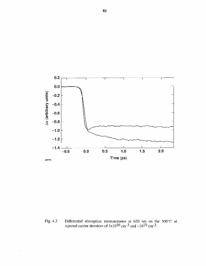
Time (ps)
Fig. 4.2 Differential absorption measurements at 620 nrn on the 500°C at injected carrier densities of 5x1 0 ti and - 10 ~ r n - ~ .

carrier injection. This results from scattering of carriers out of their initial excited
states. The relatively large width of the peak is due to the fact that carriers leave
slowly the as-excited states through carrier-carrier and LO-phonon scattering.
Taking into account the spectral extend of the 100 femtosecond pulses at 2 eV, the
electron distributions excited from the heavy and light hole bands overlap, creating
an effective carrier distribution that extends from - 100 meV to -50 meV above the
band edge. Fast carrier-carrier scattering will also broaden this distribution during
photo-excitation. Thus, the phase space available for scattering is appreciably
reduced. This leads to the observed small amplitude and relatively slow relaxation.
Exciting carriers close to the bottom of the conduction band, allows the
observation of the effects of Fermi level increasing with carrier density to be
observed. In Figure 4.2(b) we show the same experiment performed at an injected
carrier density of - 1 0 ~ 9 cm-3. This value is determined form the beam spot size,
the average power and the absorption coefficient at 2 eV. At these high densities,
the small fast relaxation disappears. Instead, the bleaching continues to increase
slowly after photoexcitation. This is the result of the slow relaxation of holes
towards the bottom of the valence band. At ~ ~ ~ - 1 0 ' ~ ~ m - ~ , electron
thermalization through carrier-carrier scattering takes place in less than 100 fs.8,9
Thus, the electron distribution is expected to contribute the most to the observed
bleaching within the pump pulsewidth. Because of their mass, heavy holes are
excited in a relatively narrow energy range even for a wide distribution of wave
vectors. Therefore, the relaxation in energy of the heavy holes is not dramatic [7].
Additionally, the initial average hole energy (-22 meV) is very close to the thermal
energy, indicating that heavy hole relaxation is minimal. The light holes on the
other hand, have an average thermal energy of 42 meV and as they relax to the
heavy hole band through intervalence band scattering, the bleaching increases. A
simple calculation of the band filling factor shows that at these high injected carrier
densities, the contribution of the heavy hole transition to the percentage change of
absorption is twice that of the light hole, leading to a net positive contribution to
bleaching. The limited phase space available for hole scattering due to the high
injected carrier density, also slows down the relaxation of holes. Recent
measurements on GaAs,[lO] have shown that heavy holes thermalize with the
lattice at -500 fs.
For excitation low in the conduction band additional effects such as band
gap renormalization and Coulomb enhancement, have to be taken into account.
Both processes increase the excited carrier density, and band renormalization also
broadens the excited distributions. Coulomb enhancement is a band edge
phenomenon, and for sufficiently high excitation energy ceases to be important.
Band renormalization in contrast, continues to grow in importance for hotter initial
electron distributions, and the canceling effect of Coulomb enhancement becomes
smaller. The bandgap will shrink and band renormalization will slow the apparent
relaxation and broaden the carrier distribution. It seems likely that this aspect of
band gap renormalization will make its greatest contribution for excitation higher
in the conduction band, and not at the band edge. Bair [6] have performed Monte
Carlo simulations for similar conditions in the case of GaInAs. They have shown
that for a cooling carrier distribution the effects of the two processes are opposite,
with bandgap renormalization slowing the carrier relaxation. Additionally, the
dominant contributions to the observed signal for the first 400 fs are from the
heavy holes, in contrast to excitation at higher energies where holes contribute
only on much shorter time scales.
In order to examine in more detail the carrier dynamics at high injected
carrier densities we performed pump-probe measurements with 2 eV pump and
WLC probe. The results are shown in Figure 4.3. The absorption change is
extracted from the transmission and reflection measurements by inverting the
Fabry-Perot formulas as described in Chapter 2. We observe absorption bleaching
at all wavelengths from 570 nm to 670 nm. In agreement with the results of Figure
4.2, we do not observe any relaxation at any wavelength. Instead the behavior is
qualitatively the same for all probe wavelengths. This is due to the large density of
injected carriers which saturates the involved transitions within the pulse width. In
spite of the fact that the band gap is at 1.89 eV, (656 nm), we observe bleaching at
-40 meV below the gap (670 nm probe wavelength). This is due to the
renormalization of the bandgap. Using an empirical formula [ l 11, the reduction of
the bandgap due to band gap renormalization is
AE (N) = 0, g
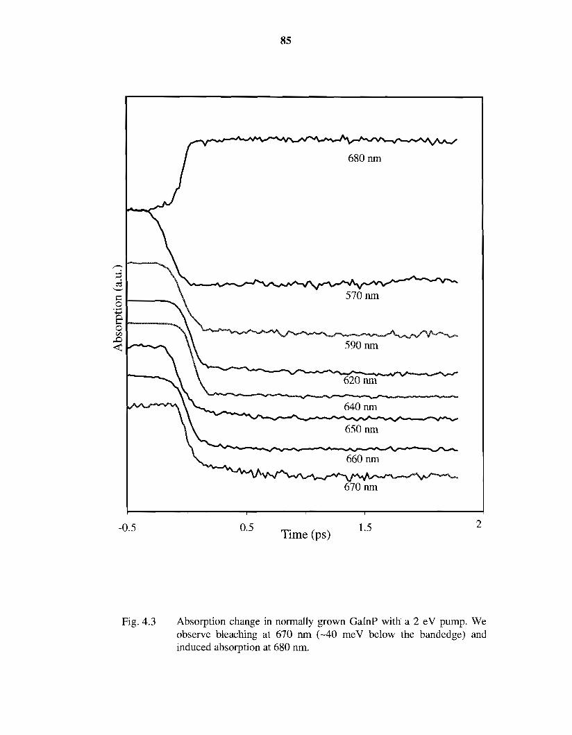
Time (ps) 1.5
Fig. 4.3 Absorption change in normally grown GaInP with a 2 eV pump. We observe bleaching at 670 nm (-40 meV below the bandedge) and induced absorption at 680 nm.

where E, is the static dielectric constant of the material, c is a fitting parameter and
Ncr is a critical carrier density. The values of some of these parameters were
extrapolated from those of GaAs since there are no data available for GaInP. Using
the above formula, we estimate the band gap renormalization to be 32 meV, in
good agreement with our results. At 680 nm the probe photons are not energetic
enough to cause a transition to the conduction band even after renormalization,
and we observe an increase in absorption. This increase is due to free carrier
absorption which becomes possible after carrier injection. The absorption change
at 680 nm is 462 cm-1, and for an injected carrier density of 1019 cm-3 we
estimate the free carrier absorption cross section to be o= oe+ oh=ba/n - 5x10-l7
4.3 Carrier-Carrier Scattering in Conventionally Grown GaAs and
GaInP
Time resolved spectroscopy of semiconductors has been one of the most
useful tools in the study of the dynamics of non-equilibrium carriers. Laser
excitation of semiconductors results in generation of electrons and holes with
relatively well defined kinetic energies in the conduction and valence bands
respectively. If the exciting pulse duration is less than or comparable to the fastest
scattering mechanisms then one should be able to monitor the evolution from

nonthermal to thermal distributions through carrier-carrier interaction among the
photoexcited carriers. At low injected carrier densities(<lo15 cm-3) this transition
takes on the order of picoseconds. l2 When the injected carrier density is higher (>
1017 ~ r n - ~ , more typical of semiconductor devices), the thermalization time is
much shorter(< 100 fs), as was found by a variety of optically based
experiments.Ll3- 161
Femtosecond bleaching experiments provide information about the dwell
time of the photogenerated carriers in the optically coupled states. The role of
carrier-carrier scattering is difficult to identify from the temporal behavior of the
bleaching signal since it is more complicated than carrier-phonon scattering and it
does not lead to an exponential recovery of the bleaching. In a degenerate
femtosecond pump-probe experiment, very fast scattering mechanisms such as
carrier-carrier interaction will significantly broaden the as-excited electron
distribution before absorption of the pump pulse is completed. This affects the
maximum bleaching, Act,,, since the faster the carriers leave the as-excited
states, the smaller the amplitude of the bleaching is. Thus, we come to the
conclusion that by monitoring Actmax under various excitation conditions, we can
directly study carrier-carrier scattering. For example, it has been reported that
Actmax varies sublinearly with increasing injected carrier density in the case of
intrinsic GaAs[l7] and superlinearly in n-type GaAs.[l8]
In the present work we employ an experimental technique that allows us to
monitor carrier-carrier scattering with improved sensitivity. This technique consists

of monitoring the maximum absorption bleaching Aamax, in the presence of an
additional electron-hole distribution. Two pulses, the pump and the probe, are
fixed at z - O+, i.e. on the maximum of the absorption bleaching, Aam. A third
pulse, the pre-pump, centered at the same wavelength as both pump and probe
pulses, injects an additional electron-hole plasma at different time delays with
respect to the pump pulse. As the time delay increases, this additional carrier
distribution relaxes towards the bottom of the conduction band and affects Aam
accordingly. Since Aam is a direct measure of carrier-carrier scattering, this type
of experiments is designed to measure the dependence of this scattering process on
both carrier density and carrier temperature. First, we examine the behavior of
normally grown GaAs under these experimental conditions. This material, being
investigated extensively, serves as a benchmark for a comparison with GaInP.
In Figure 4.4 we present a three-pulse experiment performed on the
intrinsic GaAs thin film at the low carrier density regime. Both pump and pre-
pump pulses inject N - Npre - 3x10~6 carriers. The inset shows the signal
measured in a conventional pump and probe arrangement and the arrow indicates
the time delay in which Aam, is monitored. When an additional 3x10~6 cm-3
carriers are present, IAam,l is reduced by 5%. As the delay between the pre-
pump and pump pulses increases, there is a very fast partial recovery of the
maximum bleaching, followed by a 10 ps decay. The initial maximum bleaching
reduction results from enhanced electron-electron scattering, thus, it directly
measures the efficiency of' carrier-carrier scattering.

-2 0 10 Delay between pre-pump
and pump pulses (ps)
Fig. 4.4 Three-pulse experiment on i-GaAs thin film (d - 0.2 pm) at low injected carrier densities (N - Npre - 3 x 10 ~ m - ~ ) . The inset shows where Aa- was monitored.
When the same experiment is performed at the high carrier density regime
(N - Npre - 5x10¹⁸ ~ m - ~ ) , the result is strikingly different as can be seen in
Figure 4.5. When pre-pump and pump pulses overlap temporally we see again a
decrease in IAamml due to enhanced electron-electron scattering. After - 1 ps
however, a fast recovery causes the signal to change sign and then slowly reach a
plateau. The dwell time of the electrons increases because electron-electron
scattering becomes less efficient in the presence of a high density, thermalized
electron distribution resulting an increase in IAa-I. When the carrier density is
reduced this plateau is seen to decrease with respect to the fast feature. At -
1017 cm-3, the reversal of the signal sign does not take place at all.
Two important conclusions can be deduced from Fig. 4.4. First, electron-
electron scattering is detectable even for carrier densities as low as 3 x 1 0 ~ ~ cm-3.
Second, the interaction between the two electron distributions (with 3x10¹⁶
each) is more efficient when all electrons are in similar Bloch states. In GaAs, the 2
eV photons excite three nearly monoenergetic electron distributions from the
heavy hole(hh:c), light hole(1h:c) and spin-split-off(so:c) bands. Of these
distributions, the hh:c and 1h:c have excess energy above the intervalley scattering
threshold. As the time delay between the pre-pump and pump pulses increases,
most of the hh:c and 1h:c carriers injected by the pre-pump pulse transfer to the
satellite valleys. Scattering between electrons in the X and L valleys and electrons
in the r valley becomes less efficient due to the large difference in effective
masses. This causes the fast partial recovery seen in Fig. 4.4, since - 80% of the
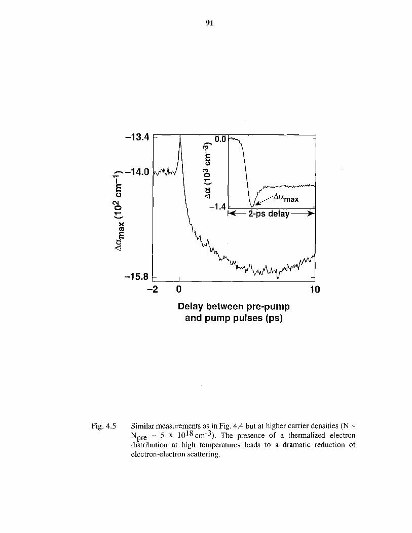
Delay between pre-pump and pump pulses (ps)
Fig. 4.5 Similar measurements as in Fig. 4.4 but at higher carrier densities (N - Npre - 5 x 1018 cm3). The presence of a thermalized electron distribution at high temperatures leads to a dramatic reduction of electron-electron scattering.
pre-pump injected electrons have transferred to the satellite valleys and only 20%
of the pump can interact efficiently with the pre-pump electrons. At later time
delays, the pre-pump carriers return to the r valley forming a colder thermalized
distribution. When the pump injected hot electrons interact with this colder
distribution, the change in momentum involved is larger than when the two
distributions occupy states with similar energy. In this single-particle picture [19]
scattering with large momentum exchange is less efficient thus leading to the slow
decay of the observed signal. When the injected carrier density is two orders of
magnitude higher, we again see an increase in electron-electron scattering when
pump and pre-pump overlap temporally on the sample, a result consistent with the
sublinear change of Actmm with density. At this high density enhanced phase-
space filling also contributes to the fast recovery. Band gap renormalization does
not contribute significantly to the observed behavior since it is primarily a band
edge phenomenon. The so:c carrier distribution injected by the pre-pump is of the
order of -1018 cm-3. As this distribution thermalizes, it populates the states with
momentum below the as-injected pump distribution, leading to increased phase
space filling and therefore less electron-electron scattering.[20] In addition,
increased screening at these high densities can also reduce the electron-electron
scattering rate. As the carriers return to the r valley, state filling and screening
lead to further reduction of electron-electron interaction which causes the large
plateau.

When 2 eV photons are used to excite electrons in GaAs, intervalley
scattering is unavoidable, complicating the interpretation of three-pulse
experiments. In order to examine electron-electron scattering without this
additional complication we performed experiments on an intrinsic In0 gGa0 5P
thin film. The bandgap of this material was determined by photoluminescence
measurements to be 1.89 eV. As a result the electrons are excited with -70 meV
excess energy and cannot transfer to the satellite valleys.
Figure 4.6 shows how the maximum change in absorption is affected by
the pre-pump pulse. When pre-pump and pump pulses overlap temporally, we
observe a sharp decrease in Actmax (increase in ATm), i.e. a reduction in
electron-electron scattering. This behavior is followed by a fast partial recovery
taking place in -0.3 ps and then a long lasting plateau. It is difficult to explain the
behavior at early time delays. Due to the fact that this is a three-beam experiment,
two beams are of the same polarization and therefore, coherent artifact can
contribute to the initial rise of the signal. Additionally, for excitation close to the
band edge, band gap renormalization also complicates the results. First, band gap
re-normalization caused by the pre-pump, induces an effective increase to the
pump and probe photons which now probe higher densities of states. This results
in a stronger bleaching. Second, this increase of the density of states increases the
phase space available for relaxation. Reduced electron-electron scattering due to
phase-space filling is believed to play a significant role at later times. We also
performed conventional pump-probe measurements at injected carrier densities
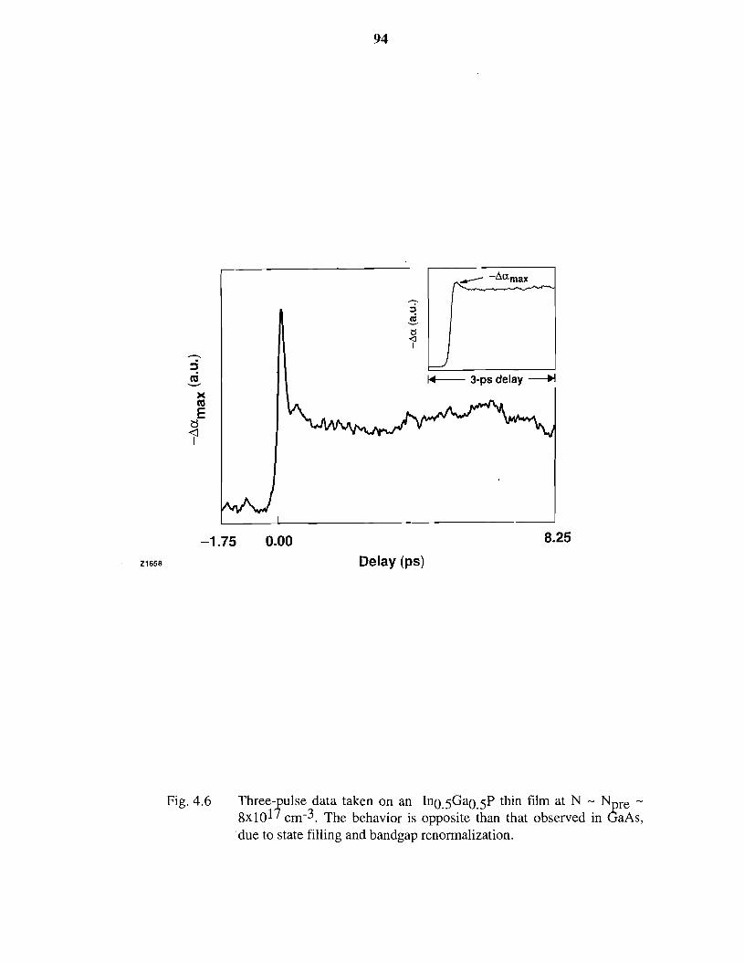
Fig. 4.6 Three-pulse data taken on an In0 5Ga0 gP thin film at N - N re - 8 x 1 0 ~ ~ ~ m - ~ . The behavior is opposite ihan that observed in & a h , 'due to state filling and bandgap renormalization.
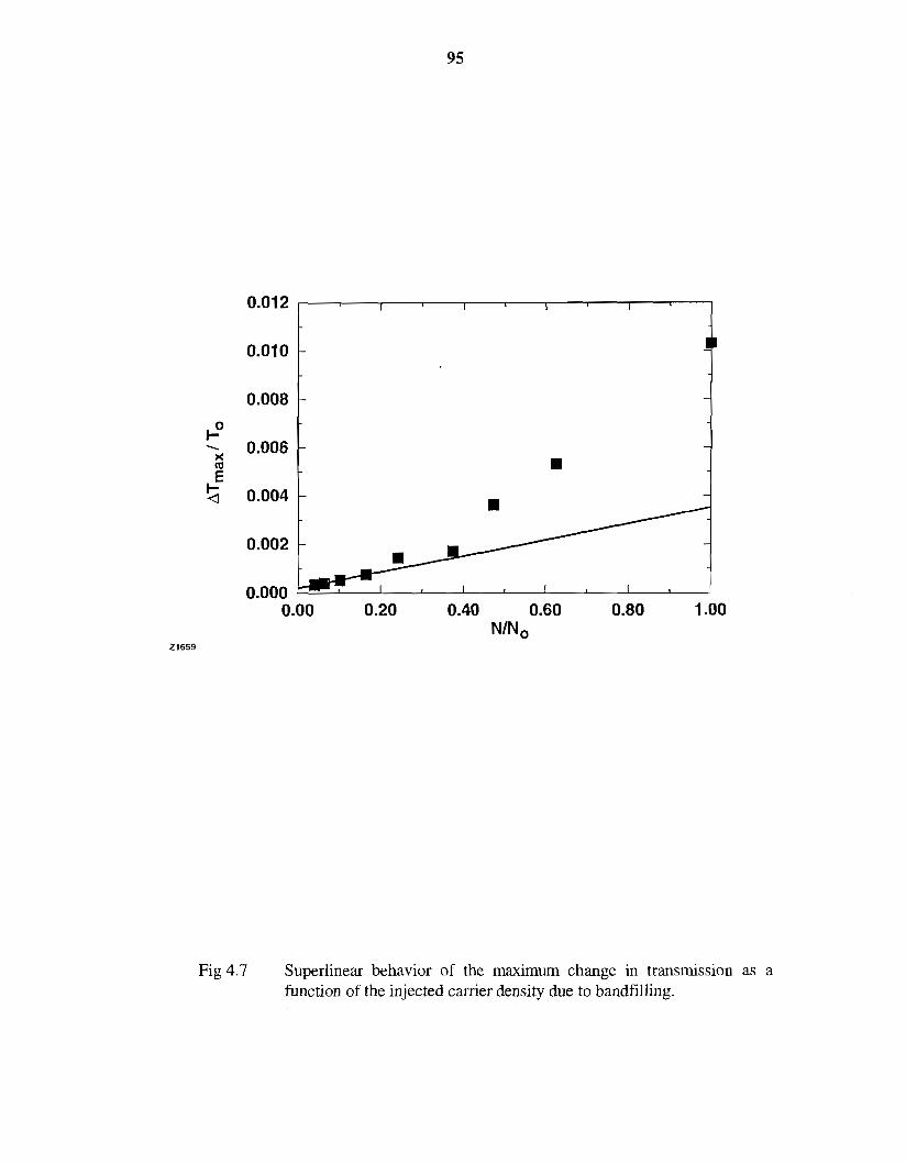
Fig 4.7 Superlinear behavior of the maximum change in transmission as a function of the injected carrier density due to bandfilling.
varying from 2 x 1 0 ~ ~ - 8x10~7 cm-3 and measured the variation of ATmn with
the carrier density as depicted in Figure 4.7. The behavior of ATm, is strongly
superlinear, a result reinforcing the hypothesis that reduced electron-electron
scattering is caused by phase-space filling. A similar superlinear behavior was
observed in heavily doped n-type GaAs [18] pumped at 2 eV.
4.4 Carrier Dynamics In Low Temperature Grown GaInP
In the previous paragraph we investigated the properties and optical
response of conventionally grown GaInP. We found that for excitation at 2 eV,
carrier relaxation is evident only at low injected carrier densities due to band
filling. Here, our goal is to perform similar measurements on material grown at low
substrate temperatures and compare its behavior to that of conventionally grown
GaInP.
The samples that were used in this study were grown by gas source
molecular beam epitaxy (GSMBE) at substrate temperatures of 300°C and 200°C.
Part of the 200°C grown sample underwent a modest in situ annealing at 450°C
for 10 min under P overpressure. X-ray diffraction measurements showed all
samples to be of good crystalline quality. Their thickness was 0.5 pm for the 300"
C sample which is equal to approximately one absorption length for 2 eV photons,

and 1 Fm for the samples grown at 200°C. The LT-grown samples did not show
any CW luminescence. Their nominal bandgap is assumed to be 1.89 eV.
Figure 4.8 shows the results of differential absorption measurements
performed at 2 eV following injection of -1019 cm-3 carriers with a 2 eV pump.
The trace of the 500°C sample is included for comparison and shows no recovery
after carrier injection due to band filling and phase space filling.[21,22] When the
growth temperature is lowered, a much faster response is observed. The recovery
of the bleaching is bi-exponential and leads to a small induced absorption plateau in
all samples. This plateau does not decay for tens of picoseconds and has also been
observed in differential transmission measurements close to the band edge of LT-
GaAs[23] and LT-InP.[24] The existence of this induced absorption plateau, is
attributed to photo-ionization of the defect centers after trapping of the
photoexcited carriers. The fact that it is a long-lived component, indicates that the
ultrafast response in LT-GaInP, similarly to what has been seen in LT-InP and LT-
GaAs, corresponds to carrier trapping and not carrier recombination which takes
place in a time scale of tens of picoseconds. In the 300°C as-grown sample, a time
constant of 1200 fs is extracted for the fast component, and it describes the dwell
time of the carriers in the as-excited states. The slower component which is 0.9 ps,
is attributed to carrier trapping as in the case of LT-InP grown at 200°C and 300"
C.[24] When the growth temperature is lowered even further to 200°C, we
observe the fastest response. This ultrafast relaxation is probably due to impurity
scattering. The component describing carrier relaxation in the as-grown sample is
21999 Time (ps)
Fig. 4.8 Bleaching at 2 eV in three samples grown at: 500°C, 200°C as-grown, 300°C as-grown and 200°C annealed at 450°C for 10 rnin. For the samples grown at lower temperatures the trapping times are 350 fs (see text), 900 fs, and 700 fs correspondingly.
found to be 50 fs (deconvoluted). It is difficult, however, to extract the carrier
trapping time from a biexponential fit, in the case of the 200°C as-grown sample,
since carrier relaxation dominates the recovery of the signal at early time delays.
This is due to the existence of a large band tail, which increases the phase space
available for carrier relaxation, as is evident by the observation of a small bleaching
component even at a probe photon energy of 1.82 eV (more than 70 meV below
the nominal band gap). This band tail is the result of the large density of point
defects due to the growth at low substrate temperatures.
A modest anneal of the 200°C grown sample at 450°C for 10 minutes,
slows the 2 eV optical response appreciably. The fast component is found to be
again 1200 fs while the slower component is 0.7 ps. This slower response after
annealing is a direct indication that the fast response in LT-GaInP is due to the
large density of point defects. No formation of phosphorus precipitates has been
observed in LT-GaInP even after an 1 hour anneal at 600°C.[3] In contrast, the
concentration of point defects is reduced, as is evident by the smaller strain
observed in the annealed sample. [3]
In order to extract the carrier trapping time in the 200°C, as-grown sample,
we compare the experiments performed at -80 meV above (620 nm probe) and
-240 meV below (750 nrn probe) the nominal conduction band edge. These
measurements are displayed in Figure 4.9. Both traces are normalized to their
peak values for comparison. The signal at 620 nm is characterized by a pulse-width
limited rise time, commensurate to the convolution of the pump and probe pulses.
22001 Time (ps)
Fig. 4.9 An ultrafast recovery of 50 fs is observed in the as-grown 200°C sample at early time delays. The trapping time, which is found to be 0.35 ps, is better resolved by a comparison of the 620 nm and the 750 nm curves. Both traces are normalized to their respective peaks.
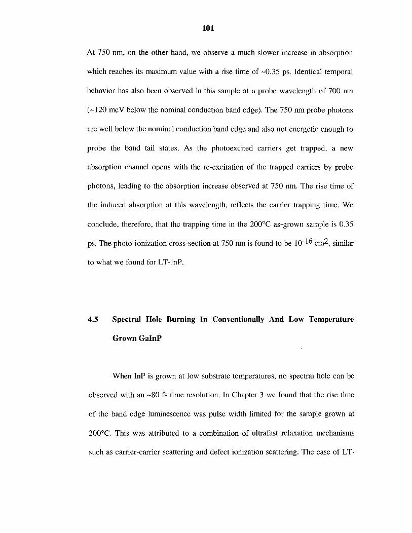
At 750 nm, on the other hand, we observe a much slower increase in absorption
which reaches its maximum value with a rise time of -0.35 ps. ldentical temporal
behavior has also been observed in this sample at a probe wavelength of 700 nm
(- 120 meV below the nominal conduction band edge). The 750 nm probe photons
are well below the nominal conduction band edge and also not energetic enough to
probe the band tail states. As the photoexcited carriers get trapped, a new
absorption channel opens with the re-excitation of the trapped carriers by probe
photons, leading to the absorption increase observed at 750 nm. The rise time of
the induced absorption at this wavelength, reflects the carrier trapping time. We
conclude, therefore, that the trapping time in the 200°C as-grown sample is 0.35
ps. The photo-ionization cross-section at 750 nm is found to be 10-l6 cm2, similar
to what we found for LT-InP.
4.5 Spectral Hole Burning In Conventionally And Low Temperature
Grown GaInP
When InP is grown at low substrate temperatures, no spectral hole can be
observed with an -80 fs time resolution. In Chapter 3 we found that the rise time
of the band edge luminescence was pulse width limited for the sample grown at
200°C. This was attributed to a combination of ultrafast relaxation mechanisms
such as carrier-carrier scattering and defect ionization scattering. The case of LT-
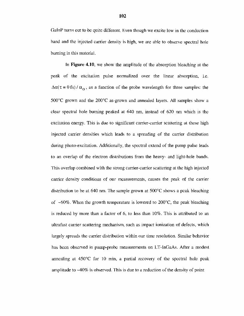
GaInP turns out to be quite different. Even though we excite low in the conduction
band and the injected carrier density is high, we are able to observe spectral hole
burning in this material.
In Figure 4.10, we show the amplitude of the absorption bleaching at the
peak of the excitation pulse normalized over the linear absorption, 1.e.
Aa(7 = 0 fs) / a. , as a function of the probe wavelength for three samples: the
500°C grown and the 200°C as-grown and annealed layers. All samples show a
clear spectral hole burning peaked at 640 nm, instead of 620 nm which is the
excitation energy. This is due to significant carrier-carrier scattering at these high
injected carrier densities which leads to a spreading of the carrier distribution
during photo-excitation. Additionally, the spectral extend of the pump pulse leads
to an overlap of the electron distributions from the heavy- and light-hole bands.
This overlap combined with the strong carrier-carrier scattering at the high injected
carrier density conditions of our measurements, causes the peak of the carrier
distribution to be at 640 nm. The sample grown at 500°C shows a peak bleaching
of -60%. When the growth temperature is lowered to 200°C, the peak bleaching
is reduced by more than a factor of 6, to less than 10%. This is attributed to an
ultrafast carrier scattering mechanism, such as impact ionization of defects, which
largely spreads the carrier distribution within our time resolution. Similar behavior
has been observed in pump-probe measurements on LT-InGaAs. After a modest
annealing at 450°C for 10 rnin, a partial recovery of the spectral hole peak
amplitude to -40% is observed. This is due to a reduction of the density of point
I I
-
---A- 200 C as-grown - --w- 200 C annealed
500 C
Probe wavelength (nm)
Figure 4.10 Contrary to LT-InP (Ref. lo), Spectral hole burning is observed in LT-GaInP and is more pronounced in the normally grown sample. Its amplitude reduces by more than a factor of 6 when a large density (>lo19 cm-3) of point defects is present, and recovers partially after annealing the sample at 450°C for 10 min.

defects introduced by the low temperature growth, as can also be seen by the
slower recovery of the bleaching signal in Figure 4.8.
A similar ultrafast spreading of the as-excited carrier distribution has also
been observed in the case of 200°C grown LT-InP.[24] No spectral hole was
observed in this material as was evident by the pulse-width limited rise time of the
band edge luminescence after excitation at 2 eV with 80 fs pulses.
4.6 Carrier Trapping vs Recombination in Low Temperature Grown
GaInP
In order to distinguish between carrier trapping in the defect levels and
carrier recombination, we performed experiments in which both pump and probe
are well below the conduction band edge of GaInP. From resistivity measurements,
the activation energy (at T-0 K) of the dominant donor in as-grown GaInP is 0.48
eV below the conduction band edge. With 840 nrn photons (-0.42 eV below the
band edge) we can therefore directly probe the defect states. After annealing, the
situation becomes a bit more uncertain. The room temperature resistivity is very
high and its value (-109 Rcm) as well as the activation energy (-0.8 eV) are
extrapolated from measurements at higher temperatures.[2]
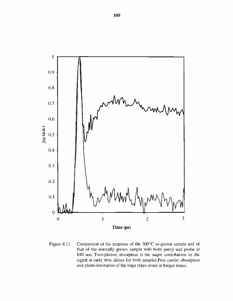
1 2 3
Time (ps)
Figure 4.11 Comparison of the response of the 300°C as-grown sample and of that of the normally grown sample with both pump and probe at 840 nm. Two-photon absorption is the major contribution to the signal at early time delays for both samples.Free carrier absorption and photo-ionization of the traps takes oveer at longer times.

In Figure 4.11 we show the results of differential absorption measurements
performed with both pump and probe at 840 nrn on the 500°C and 300°C as-
grown samples. Both layers show an increase of absorption after photoexcitation.
In the 500°C grown sample, the signal is dominated by two photon absorption
(TPA), followed by a small absorption plateau due to free carrier absorption
(FCA). By solving
where Gaussian transverse mode profiles are assumed, I and Ip are the pump and
probe intensities, P2 is the TPA coefficient, a is the free carrierabsorption cross
section, we can determine the values of P2 and a. The carrier concentration N, is
given by
In (1) we assumed that the linear absorption is negligible at the wavelength
used and in (2) that there are not memory effects between pulses. We determine
the values of the TPA coefficient to be P2 = 3.3 cm/GW, in good agreement with
the P ~ - E ~ - ~ scaling law,[25] and the induced absorption cross section to be -10-
16 cm2. This value is about an order of magnitude larger than what has been
observed for FCA in the case of GaAs[26] at similar A o / E ratios, where A w , is g
the photon energy and Eg is the bandgap energy of the material. This is probably
due to the existence of a small density of defects in the epilayer[27] whose photo-
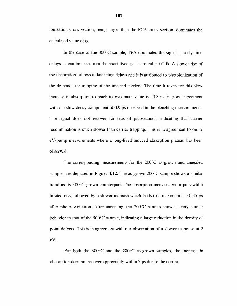
ionization cross section, being larger than the FCA cross section, dominates the
calculated value of o.
In the case of the 300°C sample, TPA dominates the signal at early time
delays as can be seen from the short-lived peak around z-0+ fs. A slower rise of
the absorption follows at later time delays and it is attributed to photoionization of
the defects after trapping of the injected carriers. The time it takes for this slow
increase in absorption to reach its maximum value is -0.8 ps, in good agreement
with the slow decay component of 0.9 ps observed in the bleaching measurements.
The signal does not recover for tens of picoseconds, indicating that carrier
recombination is much slower than carrier trapping. This is in agreement to our 2
eV-pump measurements where a long-lived induced absorption plateau has been
observed.
The corresponding measurements for the 200°C as-grown and annealed
samples are depicted in Figure 4.12. The as-grown 200°C sample shows a similar
trend as its 300c'C grown counterpart. The absorption increases via a pulsewidth
limited rise, followed by a slower increase which leads to a maximum at -0.35 ps
after photo-excitation. After annealing, the 200°C sample shows a very similar
behavior to that of the 500°C sample, indicating a large reduction in the density of
point defects. This is in agreement with our observation of a slower response at 2
eV .
For both the 300°C and the 200°C as-grown samples, the increase in
absorption does not recover appreciably within 3 ps due to the carrier
-0.2 I I I I
-0.5 0.0 0.5 1 .O 1.5 2.0 2.5
22077 Time (ps)
Figure 4.12 Similar measurements as in Figure 4.1 1 but for the 200°C as-grown and annealed samples. Even a modest anneal of 10 min at 450 "C reduces the number of traps and the response of the material is very similar to that of a conventionally grown sample.
recombination being much slower than carrier trapping. Similar behavior has been
found in LT-GaInAs and LT-GaAs. The photo-ionization cross-section of the
traps in the 200°C as-grown sample is estimated to be -5xlO-l6 cm2.
4.7 Conclusions
In this chapter we have presented the results of differential absorption
measurements at energies above and below the bandgap, on Gag 5 lIno 4gP grown
at 500°C, 300°C and 200°C. Due to the excitation low in the conduction
band,only a small relaxation of the injected carriers is observed at low densities in
the conventionally grown material. At high injected densities a slow increase of the
bleaching is observed, probably due to a slow interband relaxation of light holes.
Bandgap renormalization and Coulomb enhancement play also a role in the carrier
dynamics. Under these experimental conditions, bandgap renormalization is more
important since Coulomb enhancement is a band edge effect. Band filling together
with renormalization of the band edge, lead to behavior opposite than what is
observed for experiments where excitation high in the conduction band takes
place.
When the material is grown at low temperatures, a high density of defects
is present. These defects are probably PI, and are of a density >1019 ~ m - ~ , since
no saturation is observed in the response of the sample grown at the lowest
temperature. Trapping of the photoexcited carriers, in the low temperature grown
samples, takes place at sub-picosecond time scales with time constants of 0.35 ps
and 0.9 ps for the as-grown 200°C and 300°C samples, and of 0.7 ps for the 200"
C annealed sample. In contrast, a study below the gap, with 880 nm photons,
shows a long (>lo ps) recombination time. Re-absorption of the trapped carriers
by the probe photons leads to induced absorption with a cross section of 210-l6
cm2. A modest anneal of the 200°C sample, slows its response indicating that the
point defects are responsible for the sub-picosecond trapping times. In contrast to
what has been observed in the case of LT-InP, the burning of a spectral hole is
observed in LT-GaInP.
References
1. K. H. Bachem, Th. Lauterbach, M. Maier, W. Pletschen, and K. Winkler,
Inst. Phys. Conf. Ser. 120, 293 (1991).
2. D. C. Look, Y. He, J. Ramdani, N. El-Masry, and S. M. Bedair, Appl.
Phys. Lett. 63, 123 1 (1993).
3. Y. He, J. Ramdani, N. A. El-Masry, D. C. Look, and S. M. Bedair, J.
Electron. Mat. 22, 148 1 (1993).
4. C. Alibert, G. Bordure, A. Laugier, and J. Chevalier, Phys. Rev. B 6, 1301
(1972).

H. C. Casey, and M. B. Panish, Heterostructure Lasers (Academic, New
York, 1978), part A.
J. E. Bair, D. Cohen, J. P. Krusius, and C. R. Pollock, Phys. Rev. B 50,
4350 (1994).
M. Ulman, D. W. Bailey, L. H. Acioli, F. G. VallCe, C. J. Stanton, E. P.
Ippen, and J. G. Fujimoto, Phus. Rev. B 47, 10267 (1993).
T. Gong, P. Mertz, W. L. Nighan Jr., and P. M. Fauchet, Appl. Phys. Lett.
59, 721 (1991).
T. Gong, P. M. Fauchet, J. F. Young, and P. J. Kelly, Phys. Rev. B 44,
6542 (1991).
R. Tommasi, P. Langot, and F. VallCe Appl. Phys. Lett. 66, 1361 (1995).
B. R. Bennett, R. A. Soref, and J. A. Del Alamo, IEEE J. Quantum
Electron. QE-26, 113 (1990).
D. W. Snoke, D. W. Riihle, Y. C. Lu and E. Bauser, Phys. Rev. B 45,
10970,(1992).
T. Elsaesser, J. Shah, L. Rota and P. Lugli, Phys. Rev. Lett. 66, 1757,
(1991).
J. F. Young, T. Gong, P. J. Kelly and P. M. Fauchet, submitted to Phys.
Rev. B
P. C. Becker, H. L. Fragnito, C. H. Brito Cruz, R. L. Fork, J. E.
Cunningham, J. E. Henry and C. V. Shank, Phys. Rev. Lett. 61, 1647,
(1988).
W. H. Knox, D. S. Chelma, G. Livescu, J. E. Cunningham and J. E. Henry,
Phys. Rev. Lett. 61, 1290, (1988).
T. Gong, P. M. Fauchet, J. F. Young and P. J. Kelly, Phys. Rev. B 44
6542, (199 1).
J. F. Young, T. Gong, P. M. Fauchet, and P. J. Kelly, Phys. Rev. B 50,
2208 (1994).
plasmon emission is negligible at these carrier densities since hwp - 8
meV.
D. C. Scott, R. Binder, and S. W. Koch, Phys. Rev. Lett. 69, 347, (1992).
T. Gong, W. L. Nighan Jr, and P. M. Fauchet, Appl. Phys. Lett. 57, 2713
(1990).
J. E. Bair, D. Cohen, J. P. Krusius, and C. R. Pollock, Phys. Rev. B 50,
4355 (1994).
E. S. Harmon, M. R. Melloch, J. M. Woodall, D. D. Nolte, N. Otsuka, and
C. L. Chang, Appl. Phys. Lett. 63, 2248 (1993).
Y. Kostoulas, L. J. Waxer, I. A. Walrnsley, G. W. Wicks, and P. M.
Fauchet, Appl. Phys. Lett. 66, (1995).
E. W. Van Stryland, H. Vanherzeele, M. A. Woodall, M. J. Soileau, A. L.
Smirl, S. Guha, T. F. Bogges, Opt. Eng. 24,613 (1985).
A. S. Jordan, J. Appl. Phys. 51,2218 (1980).
R. E. Viturro, J. D. Varriano, and G. W. Wicks, Mat. Res. Soc. Symp.
Proc. 325, 5 13 (1 994).

113
CHAPTER 5
Femtosecond Carrier Dynamics In Low Temperature-Grown
GaAs
5.1 Introduction
Many semiconductor optoelectronic devices, such as photoconductive
switches and photodetectors, must operate in the multi-GHz regime. This requires
a photoinjected carrier lifetime of -1 picosecond, which can be achieved with
appropriate defect engineering. There are at least two important challenges. One is
to identify the defects and the necessary density level that not only produce such an
ultrafast response time but also yield acceptable electrical properties and long term
stability. The second is to understand the detailed role of the defects and eventually
manipulate them to achieve the desired functionality.
In the previous chapters we have investigated the dynamics of carriers in
InP and GaInP grown at low substrate temperatures. The electrical properties of
these materials are quite different. InP, when grown at low substrate temperatures,
is heavily n-type both as-grown and annealed. This severely limits its
optoelectronic applications. GaInP, on the other hand, is highly resistive in both
forms. In spite of these differences, their optical response appears to be
qualitatively the same at the lowest growth temperatures. This naturally leads to a
comparison with LT-GaAs, a material that has been more extensively studied and
characterized. As growth temperature is reduced, more As is incorporated in the
material during epitaxial growth, which leads to a high density of point defects
that form a defect band with an average energy of 0.75 eV below the conduction
band edge. In a sense, LT-GaAs is an intermediate material between LT-InP and
LT-GaInP. As-grown, it is of low resistivity (0.3-20 Rcm) due to nearest neighbor
hopping of holes in the defect band, and, like LT-InP, of limited use in electrooptic
applications. After annealing at -600°C for 10 min, its resistivity increases by a
several orders of magnitude (up to 106 Rcm) and As clusters appear. This is the
form of the material that is useful and has generated so much interest.
In this chapter we make use of the 2-eV-pump/WLC-probe system in order
to investigate carrier dynamics in two samples grown at temperatures of 250°C
and 195°C. After growth, part of the 195°C sample is annealed at 600°C for 10
minutes in As overpressure in order to investigate the effects of annealing in the
optical response. We also present some preliminary experiments performed with a
- 100 fs, 1.53-eV-pump/WLC-probe laser system on the above samples as well as
on a normally grown GaAs layer.
5.2 LT-GaAs grown at 250°C
The results of the pump-probe measurements performed on the sample
grown at a substrate temperature of 250°C are presented in Figure 5.1. The
injected carrier density is -8x10¹⁸ ~ m - ~ . The probe wavelength is varied from 570
nm to 890 nm, which corresponds to -31 meV below the room temperature band
edge of normally grown GaAs. The behavior of the sample resembles that of a
conventionally grown material throughout the range of wavelengths studied. At
the shortest wavelengths (570 nm and 590 nm), we observe a small partial
relaxation in the first 200 fs. A slower time constant takes over at longer times.
Intervalley transfer together with LO-phonon emission causes the fast relaxation.
Combining the r-X,L scattering time of -120 fs and the e-LO phonon emission
time of 180 fs yields an effective initial scattering time of 65 fs. As a result only
less than 35% of the total excited electrons ever accumulate in the as-excited
states for 2 eV excitation [I]. Most of them have already scattered away within the
pulse width since the effective initial scattering time is about half the pump
pulsewidth at room temperature. After the first -200 fs (without deconvolution)
the spin-split-off probe will make a major contribution to the signal by monitoring
bandfilling and cooling of the r-valley electron distribution [I].
As the probe photon energy becomes smaller (longer wavelengths), a slow
increase in the observed bleaching appears after -1.5 ps. It becomes visible at 650
nm and increases in magnitude up to 800 nm probe wavelength. It is due to the
return of the carriers from the L-valley and their relaxation towards the bottom of
the conduction band. About 80% of the electrons in the X valley transfer to the L-
valley and only 20% to the r-valley [2]. The X-to-L transition takes place
in- 130 fs [2] at room temperature while the L-to-r transition takes -2 ps, which

Time
+ 3 (Ps)-
Time
Figure 5.1 Pump-probe using the 2-eV-pumpNLC-probe system on LT-GaAs as-grown at 250°C.
is comparable to our observations.
As the probe wavetlength is increased to 870 nm and 890 nm, the slow rise
of the bleaching completely takes over. This behavior is commensurate with what
has been observed in GaAs grown at high temperatures (-500°C) and it is due to
band filling from the carriers returning from the sattelite valleys. We do not see any
short lived increase in absorption around z-0 fs which has been attributed to band
gap renormalization in the case of the conventionally grown material. Bleaching
due to band filling dominates the signal even at z-0 fs, indicating that a strong
scattering mechanism has extended the carrier distribution close to the band edge.
This is in agreement to what we have observed in other materials such as LT-InP
and LT-GaInP. Similar results have been seen in the case of LT-GaInAs.
The absorption plateau at longer time delays, which has been seen in LT-
InP and LT-GaInP and is attributed to re-absorption of the probe photons by the
trapped carriers, is not observed within the 3 ps time window shown in Figure 5.1.
We performed experiments at time delays of up to 15 ps but we were not able to
see any induced absorption.
We need to note that there is some uncertainty of the order of 50 K, in
determining the temperature of the substrate during growth. A higher growth
temperature leads to a lower density of point defects. This low defect density, in
turn, can be saturated at our experimental conditions of high injected carrier
densities, leading to an optical response that resembles that of the conventionally
grown material. This would put an upper bound to the defect density in this sample
at -1018 ~ m - ~ . Saturation of the traps at high injected carrier densities has also
been observed in LT-InP grown at 300°C (chapter 3). Unfortunately, it is
difficult to test this hypothesis with the 2-eV-pump/WLC-probe system since a
reduction of the injected carrier density leads to fast deterioration of the signal-to-
noise ratio due to the low repetition rate of the laser system.
5.3 LT-GaAs grown at 195°C
When the growth temperature is lowered from 250°C to 195"C, the transient
behavior changes appreciably. At this very low growth temperature, a total density
of defects of 102O cm-3 has been reported, mostly comprised of As antisite
defects. Of these, 5% are ionized leading to a hole density of 5x1018 cm-3 in the
defect band. The result of the measurements using the 2-eV-pump/WLC-probe
system are depicted in Figure 5.2. From 570 nm to 750 nrn the response of the
sample is qualitatively the same. A fast relaxation is observed in the first 200 fs,
followed by a slower component of -2 ps (without deconvolution). This is a much
faster response than what has been observed in the conventionally grown material
at these high injected carrier densities. For example, after a fast partial relaxation
due to intervalley transfer, the signal at 2 eV is dominated by the spin-split-off
transition. At high injected carrier densities, this transition is saturated leading to a
plateau that does not recover for tens of picoseconds. In LT- GaAs, as in LT-InP,
the bleaching signal gives way to an induced absorption plateau at about 3 ps after

Figure 5.2 Pump-probe using the 2-eV-pump/WLC-probe system on LT-GaAs as-grown at 195OC (see text for details).
the maximum bleaching.
At about 3 1 meV below the band gap (890 nm) we observe a fast recovery
of the signal. At this probe wavelength, the kinetic energy of the carriers is
neglidgible and the deca.y time observed is due to carrier trapping. A single
exponential fit of the data., shown in Figure 5.3, yields a trapping time of 1.4 ps.
Annealing the 195°C-grown sample at 600°C for 10 min under As
overpressure changes the optical response towards that of the conventionally
grown material. The resullts of our experiments using the 2-eV-pump~WLC-probe
system are shown in Figure 5.4. The bleaching at the shortest wavelengths (590
nm - 620 nm) recovers th.rough two components, in a manner similar to what has
been observed in the case of the as-grown 250°C sample. At 650 nrn a slow
increase of the bleaching is observed, which keeps increasing in amplitude up to
the 800 nm probe wavelength. This component is due to the relaxation of the
carriers excited at 2 eV to the bottom of the conduction band and also to the
return of the carriers frorn the satellite valleys. At 870 nm, which corresponds to
the room temperature unperturbed band edge of high temperature grown GaAs,
the slowly increasing c:omponent completely takes over. When the probe
wavelength is increased even further to 890 nm, an increase of the absorption is
observed around zero time delay. This initial increase of absorption below the band
edge is attributed to band gap renormalization and plasma screenning of Coulomb
interactions. A similar observation was made by Shank et al. at low temperatures
and with 0.5 ps time resolution and by Gong et al. at room temperature and sub-
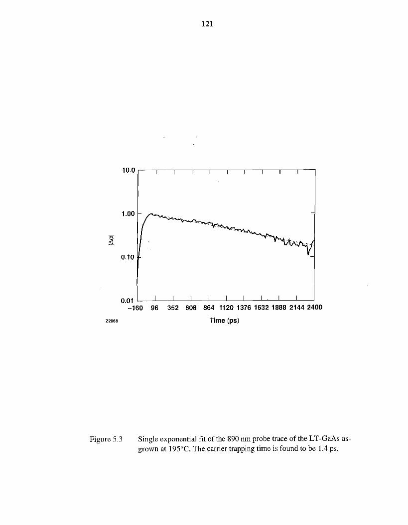
Figure 5.3 Single exponential fit of the 890 nm probe trace of the LT-GaAs as- grown at 195OC. The carrier trapping time is found to be 1.4 ps.
10.0 I 1 I I I I I I I
- a d -
0.01 -160 96 352 608 864 1120 1376 1632 1888 2144 2400
22068 Time (ps)
I I I I I . I I
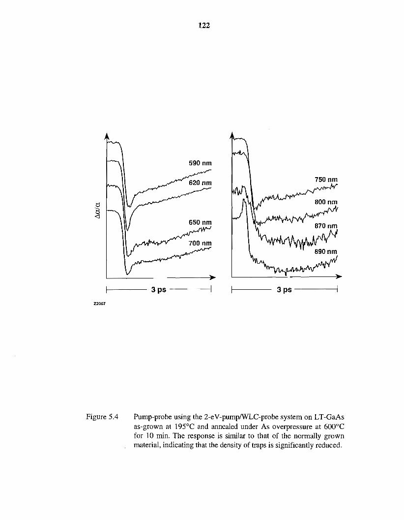
750 nrn
Figure 5.4 Pump-probe using the 2-eV-pump~WLC-probe system on LT-GaAs as-grown at 195OC and annealed under As overpressure at 600°C for 10 min. The response is similar to that of the normally grown material, indicating that the density of traps is significantly reduced.
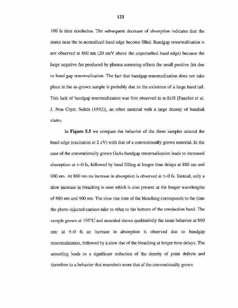
100 fs time resolution. The subsequent decrease of absorption indicates that the
states near the re-normalized band edge become filled. Bandgap renormalization is
not observed at 860 nm (20 meV above the unperturbed band edge) because the
large negative Aa producled by plasma screening offsets the small positive Aa due
to band gap renormalization. The fact that bandgap renormalization does not take
place in the as-grown sample is probably due to the existence of a large band tail.
This lack of bandgap renormalization was first observed in a-Si:H [Fauchet et al.
J. Non Cryst. Solids (1992)], an other material with a large density of bandtail
states.
In Figure 5.5 we compare the behavior of the three samples around the
band edge (excitation at 2 eV) with that of a conventionally grown material. In the
case of the conventionally grown GaAs bandgap renormalization leads to increased
absorption at 7-0 fs, followed by band fillling at longer time delays at 880 nm and
900 nm. At 860 nm no increase in absorption is observed at 7-0 fs. Instead, only a
slow increase in bleaching is seen which is also present at the longer wavelengths
of 880 nm and 900 nm. The slow rise time of the bleaching corresponds to the time
the photo-injected carrier:; take to relax to the bottom of the conduction band. The
sample grown at 195OC and annealed shows qualitatively the same behavior at 890
nrn: at 7-0 fs an increase in absorption is observed due to bandgap
renormalization, followed by a slow rise of the bleaching at longer time delays. The
annealing leads to a significant reduction of the density of point defects and
therefore to a behavior that resembels more that of the conventionally grown
Figure 5.5
500°C grown
Comparison of the bandedge response of four samples grown at , different conditions: 500°C, 250°C as-grown, 195°C as-grown, and
195°C annealed.
material. The behavior of the 250°C as-grown sample is very similar to the
normally grown, and the 195°C grown and annealed samples apart from one
difference: no bandgap renormalization is evident at 7-0 fs. The behavior of the as-
grown 195°C sample, on the other hand, is drastically different from that of the
above mentioned samples. The maximum of the bleaching is reached within the
pulse width, indicating a carrier distribution that extends to the bottom of the
conduction band within our time resolution. Thus no spectral hole burning should
be observed in this sample, in agreement to what we have observed in the case of
the LT-InP. As in the 250°C sample, no renormalization of the band edge is
observed in the195"C as-grown sample, and the existence of a large bandtail is
believed to play an important role in this effect.
5.4 Carrier Dynamics Near and Below the Band Edge
In order to investigate the trapping dynamics of carriers in LT-GaAs,
experiments were performed with an amplified Ti:Sapphire laser system producing
-80 fs pulses centered at 800 nm (1.55 eV). The pulses are amplified by means of
a regenerative amplifier to several hundred pJ at a repetition rate of 1 kHz. A small
part of the amplifier output is used as the pump pulse while the rest is focused on a
sapphire window in order to create a white light continuum from which we select
the probe wavelengths by means of interference filters. The probe wavelengths
used in our experiments range from 870 nm, which is the unperturbed bandedge of
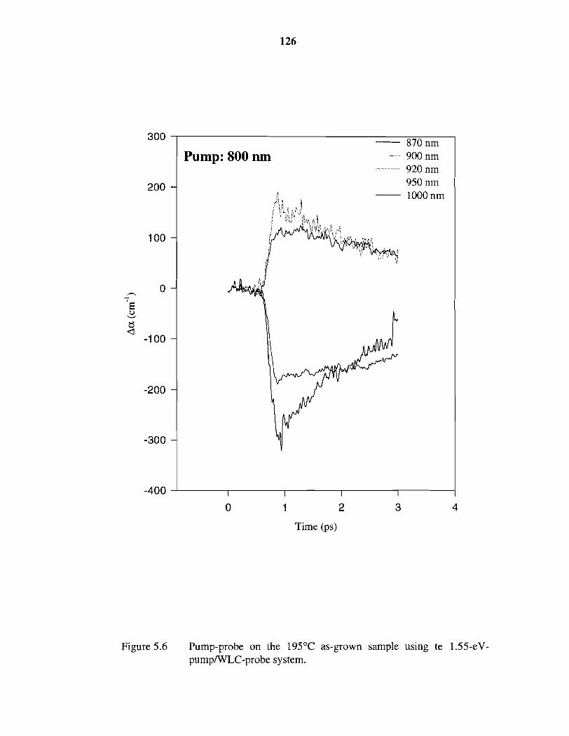
Pump: 800 nrn
-400 \ I I I
0 1 2 3 4
Time (ps)
Figure 5.6 Pump-probe on the 195°C as-grown sample using te 1.55-eV- pump1WLC-probe system.
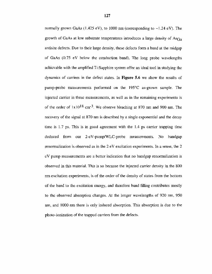
normally grown GaAs (1.425 eV), to 1000 nm (corresponding to - 1.24 eV). The
growth of GaAs at low substrate temperatures introduces a large density of ASG,
antisite defects. Due to their large density, these defects form a band at the midgap
of GaAs (0.75 eV below the conduction band). The long probe wavelengths
achievable with the amplified Ti:Sapphire system offer an ideal tool in studying the
dynamics of carriers in the defect states. In Figure 5.6 we show the results of
pump-probe measurements performed on the 195°C as-grown sample. The
injected carrier in these measurements, as well as in the remaining experiments is
of the order of lxlOLg ~ m - ~ . We observe bleaching at 870 nm and 900 nm. The
recovery of the signal at 870 nm is described by a single exponential and the decay
time is 1.7 ps. This is in good agreement with the 1.4 ps carrier trapping time
deduced from our 2-eV-pumpNLC-probe measurements. No bandgap
renormalization is observed as in the 2 eV excitation experiments. In a sense, the 2
eV pump measurements are a better indication that no bandgap renormalization is
observed in this material. This is so because the injected carrier density in the 800
nm excitation experiments, is of the order of the density of states from the bottom
of the band to the excitation energy, and therefore band filling contributes mostly
to the observed absorption changes. At the longer wavelengths of 920 nm, 950
nm, and 1000 nm there is only induced absorption. This absorption is due to the
photo-ionization of the trapped carriers from the defects.
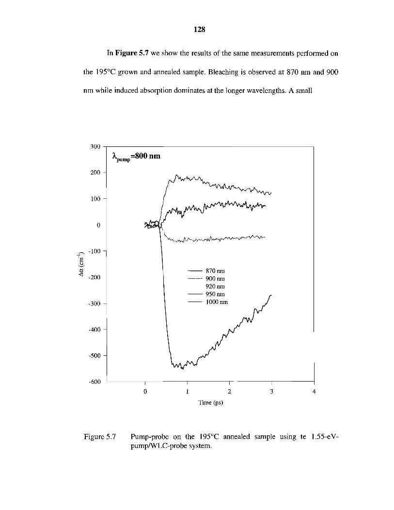
In Figure 5.7 we show the results of the same measurements performed on
the 195°C grown and annealed sample. Bleaching is observed at 870 nm and 900
nm while induced absorption dominates at the longer wavelengths. A small
-600 I I-
0 1 2 3 4
Time (ps)
Figure 5.7 Pump-probe on the 195°C annealed sample using te 1.55-eV- pump~WLC-probe sys tem.
increase of absorption is observed around zero time delay at the wavelengths of
870 nm and 900 nm (it is clearly obvious when the traces are plotted individually).
This is due to band gap renormalization and is visible in this sample since the
annealing reduces the disorder and therefore the bandtail, as compared with the as-
grown material. The recovery of the signal is slower than in the as-grown sample,
which is consistent with the lower defect density. The photo-ionization cross-
section at 1000 nm is fourid to be -5~10- l7 cm2. The same experiments performed
on the 250°C as-grown sample are shown in Figure 5.8. This material shows a
differernt behavior than ihe samples grown at 195°C (as-grown and annealed).
Bleaching is observed at 870 nm, 900 nm, 920 nm and 950 nm while induced
absorption takes over at 1000 nm. A large induced absorption at 1000 nm
indicates some resonance. It is possible that at this higher growth temperature, the
defects are of a different nature than in the material grown at the lower
temperatures. This can lead to some resonant enhancement of the absorption at
this wavelength. Indeed there is some controversy as to where the defects levels
are located in the bandgap. D. C. Look etal. [3] have measured an activation
energy of 0.65 eV for material grown at substrate temperatures of 300°C, 350°C,
and 400°C. Several other experiments have also suggested that the dominant
donor in LT-GaAs is shallower than EL2 [4-81. The results of these measurements
performed on the normally grown material are shown in Figure 5.9. They were
carried out at a smaller injected carrier density (-1017 cm-3) than the previous
measurements (-1018 cm-3). There is bandgap renormalization at 7-0 fs at

-800 I I I 4 0 1 2 3 4
Time (ps)
Figure 5.8 Pump-probe on the 250°C as-grown sample using te 1.55-eV- pump/WLC-probe system.

-600 I I I
0 1 2 3 4
Time (ps)
Figure 5.9 Pump-probe on the normally grown sample using the 1.55-eV- pump/WLC-probe system.

870 nm. This wavelength probes the bandedge of the normally grown material. As
the carriers relax, band filling leads to bleaching. The relatively slow rise of the
bleaching observed hen: is probably due to a combination of bandgap
renormalization and Coulomb enhancement. Monte Carlo calculations which take
into account these two mc:chanisms and dynamic screening, have shown that for a
cooling distribution bandgap renormalization slows the observed relaxation while
Coulomb enhancement accelerates it. The rest of the wavelengths indicate only
induced absorption due to free carrier absorption.
In conclusion we have measured the dynamics of carriers in LT-GaAs using
a 2-eV-pump/WLC-probe and a 1.55-eV-pumpfWLC-probe systems. The carrier
trapping time is found to be -1.5 ps for the 195°C as-grown material. The large
disorder in this material, increases the scattering of the photo-excited carriers
leading to a carier distribution that extends to the bottom of the conduction band
within our time resolution. Additionally, no bandgap renormalization is observed in
the as-grown material both at 250°C and at 195°C. It is recovered after annealing
of the 195°C material which leads to a significant reduction of the disorder. The
behavior of the material ilppears to be complicated when probing well below the
conduction band edge. Both the sign and the magnitude of the absorption change
indicate that the dominant defect may be different for different growth
temperatures and annealing conditions. More detailed measurements on samples
grown and annealed at different temperatures will shed light into these effects.
References
T. Gong, P. Mertz, W. L. Nighan, Jr., and P. M. Fauchet, Appl, Phys. Lett.
59,721, (1991).
S. Zollner, S. Gopalan, and M. Cardona SPIE vol. 1282, p. 78 (1990).
D. C. Look, Thin Solid Films, 2331,61, (1993).
H. J. von Bardeleben, M. 0. Manasreh, D. C. Look, K. R. Evans, and C.
E. Stutz, Phys. Rev. B, 45, 3372, (1992).
D. C. Look, D. C. Walters, C. E. Stutz, K. R. Evans, and J. R. Sizelove, J.
Appl. Phys. 71,5981, (1992).
A. C. Warren, J. M. Woodall, P. D. Kirchner, X. Yin, F. Pollak, M. R.
Melloch, N. Otsuka, and K. Mahalingam, Phys. Rev. B, 46,4617, (1992).
H. Shen, F. C. Rong, R. Lux, J. Pamulapati, M. Taysing-Lara, M. Dutta, E.
H. Poindexter, L. Calderon, and Y. Lu, Appl. Phys. Lett., 61, 1585,
(1 992).
D. C. Look, J. T. Grant, and J. R. Sizelove, Appl. Phys. Lett., 61, 1329,
(1992).
J. E. Bair, D. Cohen, J. P. Krusius, and C. R. Pollock, Phys. Rev. B, 50,
4355, (1994).

134
CHAPTER 6
Conclusions and Future Directions
GaAs layers grown by molecular beam epitaxy (MBE) at substrate
temperatures of 200°C-400°C, well under the normal growth temperature of 600"
C, exhibit unique properti'es and can be profitably used in a variety of applications
such as buffer layers for metal-semiconductor field effect transistors (FETs), gate
insulator layers for metal-insulator-semiconductor FETs, and channel layers in fast
photoconductive switches;. The most outstanding features of LT-GaAs are very
high point defect densities e.g. about 102O A S C ~ centers per cm3 in the 200°C
material and a large concentration (-1017 cm-3) of As precipitates after annealing
for 10 min at 600°C. 0the:r 111-V materials, such as AlGaAs, InAlAs, InGaAs, InP,
GaInP, and Gap have also been grown at low substrate temperatures and some
have shown promise for applications.
In this work we fcbcused on three materials which have properties that span
the spectrum of the observed material properties in LT 111-V compounds: InP,
GaInP, and GaAs. InP exhibits low resistivity in both its as-grown and annealed
forms due to the fact that P h , the dominant defect, has an ionization level
degenerate with the conduction band. GaInP exhibits high resistivity both as-
grown and annealed while GaAs is low resistivity when as-grown and it becomes
resistive after annealing.
How do these differences in electrical properties affect the optical response
of the materials? We showed that all these compounds exhibit a very similar
behavior: ultrafast scattering due to the disorder in the material spreads the carrier
distribution within -100 f!; to the bottom of the conduction band which makes the
observation of spectral hole burning at least problematic. In all cases, carrier
relaxation is followed by carrier trapping with recombination taking place at longer
time scales.
What happens to the carriers after photoexcitation? Is trapping or
recombination the observed ultrafast response in these materials? The assumption
implicit in most work up to now is that recombination is the cause of the fast
response. Our pump-probe measurements in conjunction with up-conversion
luminescence measurements show clearly that carrier trapping causes the fast
response. The trapping times in these materials are measured to be -350 fs for InP
and GaInP, and 1.4 ps for GaAs. Carrier recombination is a much slower process
that takes place in tens of picoseconds. This also leads to an induced absorption
plateau due to re-excitation of the trapped carriers which can lead to complications
in optoelectronics applications such as high bit rate optical communications
components.
The course of this research has uncovered more questions than it has
answered, as is often the case, and therefore much remains to be done. It is also
quite likely that new questions will arise faster than satisfactory answers can be
obtained for the few questions presented here. What happens when excitation close
to the band edge takes pllace? How does the behavior change? When the probe
wavelengths are well below the band edge, the change in the index of refraction
becomes significant. How large is the change in the index of refraction and how
does its magnitude and sign correlate with the observed changes in the absorption
coefficient? These are que:stions that can be answered with future experiments. A
detailed study of the carrier dynamics as a function of annealing would also yield
useful information about the physical effects determining the behavior of these
materials. For example, it has been observed [I.] that the intensity of midgap
luminescence (1.39 eV and 1.24 eV) in LT-GaAs, increases with annealing. Time
resolving the dynamics of this midgap luminescence will answer important
questions about the changes occuring in the material after annealing.
Of direct technological implication would be materials that are of high
resistivity, good crystalline quality, and have a bandgap that corresponds to 1.55
pm, an important wavelength for optical communications. In order to achieve that,
changes in composition a.re necessary which unavoidably lead to changes in the
position of the valence an~d conduction bands. Intuitively, the valence band is more
rigid than the conduction. Upon any perturbation that causes changes in volume,
the change in conduction band is larger than the change in valence band.
Theoretical and experimental work confirm this picture: the change in bandgap
energy is mostly due to changes in conduction band energy. Similar concepts apply

GaAs Gao.5Ino.sP InP Gao,471no.53As GaSb or
AlGaSb
Known to be Known to be Expected to be of Expected to be of high n-type high resistivity P-tY Pe resistivity
Figure 6.1 Schematic of the expected behavior of other 111-V compounds grown at low substrate temperatures.
to shallow donor and acce:ptor states where the impurity potential is dominated by
the long range (Coulomb) term. The case of the deep defects, which are dominant
in LT materials, is different. A deep level originates from the central-cell defect
potential which is very strong within the effective radius of the defect. It follows
that as the material composition is altered to achieve smaller bandgaps, the
position of the defects remains roughly unaltered. Therefore, appropriate defect
engineering can lead to materials relevant to optical communications wavelengths.
Some candidates can be seen in Figure 6.1 [2].
It is hopped that the techniques and observations presented in this thesis
will help guide future endeavors in this rich and not yet fully explored field.
References
1. I. Ohbu, M. Takahama, and K. Hiruma, Appl. Phys. Lett. 61, 1679, (1992).
2. G. Wicks, (private communication).


![PbTe thin films grown by femtosecond pulsed laser deposition. · electrodeposition [5], molecular beam epitaxy [6] and pulsed laser deposition [7,8,9 ] More recently, PbTe grown in](https://img.pdfslide.net/doc/110x75/5c0d44a109d3f247038d61bf/pbte-thin-films-grown-by-femtosecond-pulsed-laser-electrodeposition-5-molecular.jpg)