Embed Size (px)
Citation preview

General DescriptionThe MAX1996A integrated controller is optimized todrive cold-cathode fluorescent lamps (CCFLs) usingsynchronized full-bridge inverter architecture.Synchronized drive provides near sinusoidal waveformsover the entire input range to maximize the life ofCCFLs. The controller also operates over a wide input-voltage range with high efficiency and broad dimmingrange.
The MAX1996A includes safety features that limit thetransformer secondary voltage and protect against sin-gle-point fault conditions including lamp-out and short-circuit faults.
The MAX1996A regulates the CCFL brightness in threeways: linearly controlling the lamp current, digital pulse-width modulating (DPWM) the lamp current, or usingboth methods simultaneously to achieve the widestdimming range (>30:1). CCFL brightness can be con-trolled with either an analog voltage or a 2-wireSMBus™-compatible interface. The MAX1996A directlydrives the four external N-channel power MOSFETs ofthe full bridge inverter. An internal 5.3V linear regulatorpowers the MOSFET drivers, the synchronizable DPWMoscillator, and most of the internal circuitry.
The MAX1996A has the same pin configuration as theMAX1895, but with modified SMBus slave address(0x58) and command bytes. In addition, the lamp-outprotection timer has been reduced to approximately 1sand the DPWM frequency is guaranteed from 200Hz to220Hz over the operating temperature range withoutexternal components or trimming. The MAX1996A isavailable in the space-saving 28-pin thin QFN packageand operates over a -40°C to +85°C temperaturerange.
ApplicationsNotebook Computers
Multibulb LCD Monitors
Portable Display Electronics
Features SMBus Slave Address (0x58) for Wide Dimming
Range Inverters
Guaranteed 200Hz to 220Hz DPWM Frequency
Externally Synchronizable DPWM Frequency
Lamp-Out Protection with 1s Timeout
Synchronized to Resonant FrequencyGood Crest Factor for Longer Lamp Life Ensures Maximum Strike Capability
High Power-to-Light Efficiency
Wide Dimming Range (3 Methods)Lamp Current Adjust: >3 to 1DPWM: >10 to 1Combined: >30 to 1
Feed-Forward for Fast Response to Step Changeof Input Voltage
Wide Input-Voltage Range (4.6V to 28V)
Transformer Secondary Voltage Limiting toReduce Transformer Stress
Protected Against Short-Circuit and Other Single-Point Faults
Dual-Mode Brightness Control Interface
Small Footprint 28-Pin Thin QFN (5mm 5mm)Package
MA
X1
99
6A
High-Efficiency, Wide Brightness Range, CCFL Backlight Controller
________________________________________________________________ Maxim Integrated Products 1
28 27 26 25 24 23 22
V CC
BATT
CCV
CCI
IFB
N.C.
VFB
8 9 10 11 12 13 14
SH/S
US N.C.
N.C.
N.C.
VDD
PGND GL
2
15
16
17
18
19
20
21
GL1
GH1
LX1
BST1
BST2
LX2
GH2
7
6
5
4
3
2
1
CTL/SCL
CRF/SDA
MODE
GND
MINDAC
REF
ILIM
MAX1996A
THIN QFN5mm × 5mm
TOP VIEW
Pin Configuration
19-2267; Rev 1; 10/02
For pricing, delivery, and ordering information, please contact Maxim/Dallas Direct! at 1-888-629-4642, or visit Maxim’s website at www.maxim-ic.com.
Ordering InformationPART TEMP RANGE PIN-PACKAGE
MAX1996AETI -40°C to +85°C 28 Thin QFN 5 5
MAX1996AEGI* -40°C to +85°C 28 QFN 5 5
SMBus is a trademark of Intel Corp.
*Contact factory for availability.

MA
X1
99
6A
High-Efficiency, Wide Brightness Range, CCFL Backlight Controller
2 _______________________________________________________________________________________
ABSOLUTE MAXIMUM RATINGS
Stresses beyond those listed under “Absolute Maximum Ratings” may cause permanent damage to the device. These are stress ratings only, and functionaloperation of the device at these or any other conditions beyond those indicated in the operational sections of the specifications is not implied. Exposure toabsolute maximum rating conditions for extended periods may affect device reliability.
BATT to GND..........................................................-0.3V to +30VBST1, BST2 to GND ...............................................-0.3V to +36VBST1 to LX1, BST2 to LX2 ........................................-0.3V to +6VGH1 to LX1 ...............................................-0.3V to (BST1 + 0.3V)GH2 to LX2 ...............................................-0.3V to (BST2 + 0.3V)VCC, VDD to GND .....................................................-0.3V to +6VREF, ILIM to GND.......................................-0.3V to (VCC + 0.3V)GL1, GL2 to GND.......................................-0.3V to (VDD + 0.3V)MINDAC, IFB, CCV, CCI to GND .............................-0.3V to +6V
MODE to GND...........................................................-6V to +12VVFB to GND.................................................................-6V to +6VCRF/SDA, CTL/SCL, SH/SUS to GND ......................-0.3V to +6VPGND to GND .......................................................-0.3V to +0.3VContinuous Power Dissipation (TA = +70°C)
28-Pin QFN (derate 20.84mW/°C above +70°C) .......1667mWOperating Temperature Range ...........................-40°C to +85°CStorage Temperature Range .............................-65°C to +150°CLead Temperature (soldering, 10s) .................................+300°C
ELECTRICAL CHARACTERISTICS(VBATT = 12V, MINDAC = GND, VCC = VDD, VSH/SUS = 5.3V, TA = 0°C to +85°C, unless otherwise noted. Typical values are at TA = +25°C.) (Note 1)
PARAMETER CONDITIONS MIN TYP MAX UNITS
VCC = VDD = VBATT 4.6 5.5VBATT Input Voltage Range
VCC = VDD = open 5.5 28V
VBATT = 28V 3.2 6.0VBATT Quiescent Current V SH /SUS = 5.5V
VBATT = VCC = 5V 6mA
VBATT Quiescent Current, Shutdown SH /SUS = 0 6 20 µA
VCC Output Voltage, Normal OperationV SH /SUS = 5.5V, 6V < VBATT < 28V0 < ILOAD < 20mA
5.00 5.35 5.50 V
VCC Output Voltage, Shutdown SH /SUS = GND, no load 3.5 4.6 5.5 V
VCC rising (leaving lockout) 4.5VCC Undervoltage Lockout (UVLO)Threshold VCC falling (entering lockout) 4.0
V
VCC UVLO Lockout Hysteresis 200 mV
VCC Power-On Reset (POR) Threshold Rising edge 0.90 1.75 2.70 V
VCC POR Hysteresis Falling edge 50 mV
REF Output Voltage, Normal Operation 4.5V < VCC < 5.5V, ILOAD = 40µA 1.96 2.00 2.04 V
GH1, GH2, GL1, GL2 On-Resistance ITEST = 100mA, VCC = VDD = 5.3V 2 6 Ω
GH1, GH2, GL1, GL2 Maximum OutputCurrent
1 A
BST1, BST2 Leakage Current BST_ = 12V, LX_ = 7V 5 µA
Input Resonant Frequency Guaranteed by design 20 300 kHz
Minimum Off-Time 210 315 420 ns
Maximum Off-Time 21.0 31.5 42.0 µs
Maximum Current-Limit ThresholdLX1-GND, LX2-GND (Fixed)
ILIM = VCC 180 200 220 mV
VILIM = 0.5V 80 100 120Maximum Current-Limit ThresholdLX1-GND, LX2-GND (Adjustable) VILIM = 2.0V 370 400 430
mV
MA
X1
99
6A
High-Efficiency, Wide Brightness Range, CCFL Backlight Controller
_______________________________________________________________________________________ 3
ELECTRICAL CHARACTERISTICS (continued)(VBATT = 12V, MINDAC = GND, VCC = VDD, VSH/SUS = 5.3V, TA = 0°C to +85°C, unless otherwise noted. Typical values are at TA = +25°C.) (Note 1)
PARAMETER CONDITIONS MIN TYP MAX UNITS
Minimum Current-Crossing ThresholdLX1-GND, LX2-GND
6 mV
Current-Limit Leading-Edge Blanking 210 315 420 ns
D/A Converter Resolution Guaranteed monotonic 5 Bits
MINDAC Input Voltage Range 0 2 V
MINDAC Input Bias Current -2 +2 µA
MINDAC Digital PWM Disable Threshold MINDAC = VCC 2.4 3.5 4.0 V
IFB Input Voltage Range 0 1.7 V
VMINDAC = 0V, DAC code = 11111 binary 368 388 408
VMINDAC = 0V, DAC code = 00100 binary 30 50 70IFB Regulation Point
VMINDAC = 1V, DAC code = 00000 binary 180 200 220
mV
IFB Input Bias Current -2 +2 µA
IFB Lamp-Out Threshold 125 150 175 mV
IFB to CCI Transconductance 1V < VCCI < 2.5V 100 µS
CCI Output Impedance 20 MΩVFB Input Voltage Range -2 +2 V
VFB Input Bias Current VFB = 0V -0.5 +0.5 µA
VFB Regulation Point 490 510 530 mV
VFB to CCV Transconductance 1V < VCCV < 2.7V 40 µS
VFB Zero-Voltage Crossing Threshold -10 +10 mV
CCV Output Impedance 20 MΩNo AC signal on MODE 200 210 220
32kHz AC signal on MODE 250Digital PWM Chop-Mode Frequency
100kHz AC signal on MODE 781
Hz
MODE-to-DPWM Sync Ratio fMODE/fDPWM 128
No AC signal on MODE 1.14 1.22 1.30
32kHz AC signal on MODE 1.02Lamp-Out Detection Timeout Timer(Note 2)
VIFB < 0.1V
100kHz AC signal on MODE 0.33
s
MODE Operating Voltage Range -5.5 11.0 V
MODE Input Current MODE = GND or VCC -1 +1 µA
Positive Analog Interface Mode,MODE = GND Threshold (VCTL/SCL = 0VSets Minimum Brightness)
Sync clock average value on MODE to syncDPWM oscillator, not in shutdown (Note 3)
0.6 V
Negative Analog Interface Mode,MODE = REF Threshold (VCTL/SCL = 0VSets Maximum Brightness = 0V)
Sync clock average value on MODE to syncDPWM oscillator, not in shutdown (Note 3)
1.4 2.6 V
SMBus Interface Mode, MODE = VCCThreshold
Sync clock average value on MODE to syncDPWM oscillator, not in shutdown (Note 3)
VCC -0.6
V
MA
X1
99
6A
High-Efficiency, Wide Brightness Range, CCFL Backlight Controller
4 _______________________________________________________________________________________
ELECTRICAL CHARACTERISTICS (continued)(VBATT = 12V, MINDAC = GND, VCC = VDD, VSH/SUS = 5.3V, TA = 0°C to +85°C, unless otherwise noted. Typical values are at TA = +25°C.) (Note 1)
PARAMETER CONDITIONS MIN TYP MAX UNITS
MODE AC Signal Amplitude Peak-to-peak (Note 4) 2 5 V
MODE AC Signal Synchronization Range Chopping oscillator synchronized to MODE 32 100 kHz
CRF/SDA Input Range 2.7 5.5 V
VCRF/SDA = 5.5V, SH /SUS = VCC 20CRF/SDA Input Current
VCRF/SDA = 5.5V, SH /SUS = 0V -1 +1µA
CTL/SCL Input Range 0 VCRF/SDA V
CTL/SCL Input Current MODE = REF or GND -1 +1 µA
A/D Converter Resolution Guaranteed monotonic 5 Bits
A/D Converter Hysteresis 1 LSB
SH /SUS Input Low Voltage 0.8 V
SH /SUS Input High Voltage 2.1 VSH /SUS Input Hysteresis 300 mV
SH /SUS Input Bias Current -1 +1 µA
SDA, SCL Input Low Voltage 0.8 V
SDA, SCL Input High Voltage 2.1 V
SDA, SCL Input Hysteresis 300 mV
SDA Output Low Sink Current VCRF/SDA = 0.4V 4 mA
SCL Serial Clock High Period THIGH 4 µs
SCL Serial Clock Low Period TLOW 4.7 µs
Start Condition Setup Time tSU:STA 4.7 µs
Start Condition Hold Time tHD:STA 4 µs
SDA Valid to SCL Rising-Edge SetupTime, Slave Clocking in Data
tSU:DAT 250 ns
SCL Falling Edge to SDA Transition tHD:DAT 0 ns
SCL Falling Edge to SDA Valid, ReadingOut Data
TDV 700 ns
ELECTRICAL CHARACTERISTICS(VBATT = 12V, MINDAC = GND, VCC = VDD, VSH/SUS = 5.3V, TA = -40°C to +85°C, unless otherwise noted.) (Note 1)
PARAMETER CONDITIONS MIN TYP MAX UNITS
VCC = VDD = VBATT 4.6 5.5VBATT Input Voltage Range
VCC = VDD = open 5.5 28.0V
VBATT = 28V 6VBATT Quiescent Current V SH/SUS = 5.5V
VBATT = VCC = 5V 6mA
VBATT Quiescent Current, Shutdown V SH/SUS = 0V 20 µA

MA
X1
99
6A
High-Efficiency, Wide Brightness Range, CCFL Backlight Controller
_______________________________________________________________________________________ 5
ELECTRICAL CHARACTERISTICS (continued)(VBATT = 12V, MINDAC = GND, VCC = VDD, VSH/SUS = 5.3V, TA = -40°C to +85°C, unless otherwise noted.) (Note 1)
PARAMETER CONDITIONS MIN TYP MAX UNITS
VCC Output Voltage, Normal OperationV SH/SUS = 5.5V, 6V < VBATT < 28V,0 < ILOAD < 20mA
5.0 5.5 V
VCC Output Voltage, Shutdown SH/SUS = GND, no load 3.5 5.5 V
VCC rising (leaving lockout) 4.5VCC UVLO Threshold
VCC rising (entering lockout) 4V
VCC POR Threshold Rising edge 0.9 2.7 V
REF Output Voltage, Normal Operation 4.5V < VCC < 5.5V, ILOAD = 40µA 1.96 2.04 V
GH1, GH2, GL1, GL2 On-Resistance ITEST = 100mA 10 Ω
Maximum Current-Limit ThresholdLX1-GND, LX2-GND (Fixed)
ILIM = VCC 180 220 mV
VILIM = 0.5V 80 120Maximum Current-Limit ThresholdLX1-GND, LX2-GND (Adjustable) VILIM = 2.0V 360 440
mV
IFB Input Voltage Range 0 1.7 V
IFB Regulation Point VMINDAC = 0V, DAC code = 11111 binary 335 440 mV
IFB Input Bias Current -2 +2 µA
IFB Lamp-Out Threshold 120 180 mV
VFB Input Voltage Range -2 +2 V
VFB Input Bias Current VFB = 0V -0.5 0.5 µA
VFB Regulation Point 480 540 mV
VFB Zero-Voltage Crossing Threshold -20 +20 mV
SHVSUS Input Low Voltage 0.8 V
SHVSUS Input High Voltage 2.1 V
SDA, SCL Input Low Voltage 0.8 V
SDA, SCL Input High Voltage 2.1 V
SDA Output Low Sink Current VCRF/SDA = 0.4V 4 mA
Note 1: Specifications to -40°C are guaranteed by design based on final test characterization results. Note 2: Corresponds to 256 DPWM cycles or 32768 MODE cycles.Note 3: The MODE pin thresholds are only valid while the part is operating. When in shutdown, VREF = 0 and the part only differenti-
ates between SMB mode and ADC mode. When in shutdown and with ADC mode selected, the CRF/SDA and CTL/SCLpins are at high impedance and do not cause extra supply current when their voltages are not at GND or VCC.
Note 4: The amplitude is measured with the following circuit:
VAMPLITUDE > 2V
MODE
500pF
10kΩ

MA
X1
99
6A
High-Efficiency, Wide Brightness Range, CCFL Backlight Controller
6 _______________________________________________________________________________________
1050 2015 25
VCC vs. VBATT
MAX
1996
toc0
9
VBATT (V)
V CC
(V)
1
2
3
0
5
6
4
NORMAL OPERATION
SHUTDOWN
1ms/div
STARTUP
0V
12V VBATT
VFB2V/div
IFB2V/div
MAX1996 toc04
IBATT500mA/div
1ms/div
SYNCHRONIZED DPWM(fMODE = 100kHz, DPWM = 50%)
VFB1V/div
IFB1V/div
LX110V/div
LX210V/div
MAX1996 toc05
1ms/div
SYNCHRONIZED DPWM(fMODE = 32kHz, DPWM = 50%)
VFB1V/div
IFB1V/div
LX110V/div
LX210V/div
MAX1996 toc06
2ms/div
LAMP-OUT VOLTAGE LIMITING
VFB2V/div
VSECONDARY2kV/div
IFB1V/div
MAX1996 toc07
LAMP REMOVED
200ms/div
LAMP-OUT PROTECTION
VSECONDARY2kV/div
VFB2V/div
IFB1V/div
MAX1996 toc08
1s
LAMP REMOVED
Typical Operating Characteristics(VBATT = 12V, VCTL = VCRF, VMINDAC = 1V, MODE = GND, circuit of Figure 1, Table 4.)
10µs/div
LOW INPUT-VOLTAGE OPERATION(VBATT = 8V)
IFB2V/div
VFB2V/div
LX110V/div
LX210V/div
MAX1996 toc01
10µs/div
HIGH INPUT-VOLTAGE OPERATION(VBATT = 20V)
IFB2V/div
VFB2V/div
LX110V/div
LX210V/div
MAX1996 toc02
20µs/div
FEED-FORWARD COMPENSATION
10VVBATT
20V
VFB2V/div
IFB2V/div
MAX1996 toc03
LX110V/div

MA
X1
99
6A
High-Efficiency, Wide Brightness Range, CCFL Backlight Controller
_______________________________________________________________________________________ 7
5.40
5.100.01 0.1 10 100
VCC LOAD REGULATION
5.15
5.30
5.35
MAX1996 toc10
ILOAD (mA)
V CC
(V)
1
5.20
5.25
NORMAL OPERATION
SHUTDOWN
4.6
4.0
4.1
4.4
4.5
4.2
4.3SH
UTDO
WN
V CC
(V)
-15-40 603510 85
VCC vs. TEMPERATUREMAX1996 toc11
TEMPERATURE (°C)
V CC
(V)
5.32
5.33
5.31
5.35
5.36
5.34
SHUT
DOW
N V C
C (V
)
4.40
4.45
4.35
4.55
4.60
4.50
NORMAL OPERATION
SHUTDOWN
Typical Operating Characteristics (continued)(VBATT = 12V, VCTL = VCRF, VMINDAC = 1V, MODE = GND, circuit of Figure 1, Table 4.)
PIN NAME FUNCTION
1 ILIM
Current-Limit Threshold Adjustment. Bias ILIM with a resistive voltage-divider between REF or VCCand GND. The current-limit threshold measured between LX_ and GND is 1/5th the voltage at ILIM;ILIM adjustment range is 0V to 3V. Connect ILIM to VCC to set the default current-limit threshold to0.2V.
2 REF2V Reference Output. Bypass REF to GND with a 0.1µF capacitor. REF is discharged to GND whenshut down.
3 MINDACDAC Zero-Scale Input. VMINDAC sets the D/A converter’s minimum-scale output voltage. DisableDPWM by connecting MINDAC to VCC.
4 GNDSystem Ground. The GND input to the maximum and minimum current-limit comparators. Thecomparators sense the low-side FET NL1 and NL2 for zero-current crossing and current limit.
5 MODE
Interface Selection Input and Sync Input for DPWM Chopping. The average voltage on the MODEpin selects one of three CCFL brightness control interfaces:
MODE = VCC enables SMBus serial interface.MODE = GND enables the analog interface (positive analog interface mode), VCTL/SCL = 0V setsminimum brightness.MODE = REF enables the analog interface (reverse analog interface mode), VCTL/SCL = 0V setsmaximum brightness.
An AC clocking signal superimposed on the DC average MODE pin voltage can be used tosynchronize the DPWM chopping frequency. See Synchronizing the DPWM Frequency.
6 CRF/SDAReference and Serial Data Input. In analog interface mode, pin 6 is the reference input to the 5-bitbrightness control ADC. Bypass CRF to GND with a 0.1µF capacitor. In SMBus interface mode,SDA is an SMBus serial data input/open-drain output.
Pin Description
MA
X1
99
6A
High-Efficiency, Wide Brightness Range, CCFL Backlight Controller
8 _______________________________________________________________________________________
PIN NAME FUNCTION
7 CTL/SCLBrightness Control and Serial Clock Input. In analog interface mode, pin 7 is a CCFL brightnesscontrol input. CTL varies from 0V to REF to linearly control lamp brightness. In SMBus interfacemode, SCL is an SMBus serial clock input.
8 SH/SUSShutdown and Suspend Mode Control. In analog interface mode, pin 8 is an active-low shutdowninput. In SMBus interface mode, pin 8 is an SMBus suspend control input.
9, 10, 11, 23 N.C. No Connection. Not internally connected.
12 VDDPower Supply for Gate Drivers. Connect VDD to the output of the linear regulator (VCC). Bypass VDDwith a 0.1µF capacitor to PGND.
13 PGND Power Ground. Gate-driver current flows through this pin.
14 GL2 Low-Side FET NL2 Gate-Driver Output
15 GL1 Low-Side FET NL1 Gate-Driver Output
16 GH1 High-Side FET NH1 Gate-Driver Output
17 LX1Switching Node Connection. LX1 is the internal lower supply rail for the GH1 high-side gate driver.LX1 is also the sense input to the current comparators.
18 BST1High-Side FET NH1 Driver Bootstrap Input. Connect BST1 through a diode to VDD and through a0.1µF capacitor to LX1 (Figure 1).
19 BST2High-Side FET NH2 Driver Bootstrap Input. Connect BST2 through a diode to VDD and through a0.1µF capacitor to LX2 (Figure 1).
20 LX2Switching Node Connection. LX2 is the internal lower supply rail for the GH2 high-side gate driver.LX2 is also the sense input to the current comparators.
21 GH2 High-Side FET NH2 Gate-Driver Output
22 VFB
Lamp-Output Feedback-Sense Input. The average value on VFB is regulated during startup andopen-lamp conditions to 0.5V by controlling the on-time of high-side switches. A capacitive voltage-divider between the CCFL lamp output and GND is sensed to set the maximum average lampoutput voltage.
24 IFBLamp Current-Sense Input. The voltage on IFB is used to regulate the lamp current. If the IFB inputfalls below 150mV for 1s, then the MAX1996A signals an open-lamp fault.
25 CCI
Current-Loop Compensation Pin. CCI is the output of the current-loop transconductance amplifier(GMI) that regulates the CCFL current. The CCI voltage controls the time interval in which full-bridge applies the input voltage (BATT) to transformer network. Connect CCI to GND through a0.1µF capacitor. CCI is internally discharged to GND in shutdown.
26 CCV
Voltage-Loop Compensation Pin. CCV is the output of the voltage-loop transconductance amplifier(GMV) that regulates the maximum average secondary transformer voltage. Connect CCV to GNDwith a 10nF capacitor. The CCV voltage controls the time interval that the full bridge applies theinput voltage (BATT) to transformer network. CCV is internally discharged to GND in shutdown.
27 BATTSupply Input. Input to the internal 5.3V linear regulator that provides power (VCC) to the chip.Bypass BATT to GND with a 0.1µF capacitor.
28 VCC5.3V Linear-Regulator Output. VCC is the supply voltage for the MAX1996A. Bypass VCC to GNDwith a 0.47µF ceramic capacitor. VCC can also be connected to BATT if VBATT < 5.5V.
Pin Description (continued)

MA
X1
99
6A
High-Efficiency, Wide Brightness Range, CCFL Backlight Controller
_______________________________________________________________________________________ 9
Detailed DescriptionThe MAX1996A is optimized to drive CCFLs using asynchronized full-bridge inverter architecture. The driveto the full-bridge MOSFETs is synchronized to the reso-nant frequency of the tank circuit so that the CCFL’sfull-strike voltage develops for all operating conditions.The synchronized architecture provides near sinusoidaldrive waveforms over the entire input range to maxi-mize the life of CCFLs. The MAX1996A operates over awide input voltage range (4.6V to 28V), achieves highefficiency, and maximizes dimming range.
The MAX1996A regulates the brightness of a CCFL inthree ways:
1) Linearly controlling the lamp current.
2) Digitally pulse-width modulating (or chopping) thelamp current (DPWM).
3) Using both methods simultaneously for widest dim-ming range.
DPWM is implemented by pulse-width modulating thelamp current at a rate faster than the eye can detect.
The MAX1996A includes a 5.3V linear regulator topower the drivers for full-bridge switches, the synchro-nizable DPWM oscillator, and most of the internal cir-cuitry. The MAX1996A is very flexible and can becontrolled with an analog interface or with an SMBusinterface.
Figure 1. Standard Application Circuit
MAX1996A
REF ILIM
MIN
DAC
GND
MOD
E
CRF/
SDA
CTL/
SCL
GH2
LX2
BST2BST1
LX1
C3
C2T1
C1
C6
ON/OFF
REFERENCE INPUT
CONTROL INPUT
R3
C10
C8
C7
C5
D2-1
C9
D2-2
GH1
GL1
VCC
BATT
CCV
CCI
IFB
VFB
GL2
PGND
VDD
SH/S
US
NL1 NL2
NH1 NH2
C4 R2
R4
R1
D1
VIN5V TO 28V
CCFL

MA
X1
99
6A
High-Efficiency, Wide Brightness Range, CCFL Backlight Controller
10 ______________________________________________________________________________________
Resonant OperationThe MAX1996A drives the four N-channel powerMOSFETs that make up the zero-voltage switching(ZVS) full-bridge inverter as shown in Figure 1. The LX1and LX2 switching nodes are AC coupled to the prima-ry side of the transformer.
Assume that NH1 and NL2 are turned on at the begin-ning of the cycle as shown in Figure 2(a). The primarycurrent flows through MOSFET NH1, DC blocking capC2, the primary side of transformer T1, and finally MOS-FET NL2. During this interval, the primary current rampsup until the controller turns off NH1. When NH1 is off,the primary current forward biases the body diode ofNL1 and brings the LX1 node down as shown in Figure2(b). When the controller turns on NL1, its drain-to-source voltage is near zero because its forward-biasedbody diode clamps the drain. Since NL2 is still on, theprimary current flows through NL1, C2, the primary sideof T1, and finally NL2. Once the primary current drops
to the minimum current threshold (6mV/RDSON), thecontroller turns off NL2. The remaining energy in T1charges up the LX2 node until the body diode of NH2 isforward biased. When NH2 turns on, it does so withnear zero drain-to-source voltage. The primary currentreverses polarity as shown in Figure 2(c), beginning anew cycle with the current flowing in the opposite direc-tion, with NH2 and NL1 on. The primary current rampsup until the controller turns off NH2. When NH2 is off,the primary current forward biases the body diode ofNL2, and brings the LX2 node down as shown in Figure2(d). After the LX2 node goes low, the controller loss-lessly turns on NL2. Once the primary current drops tothe minimum current threshold, the controller turns offNL1. The remaining energy charges up the LX1 nodeuntil the body diode of NH1 is forward biased. Finally,NH1 losslessly turns on, beginning a new cycle asshown in Figure 2(a).
Figure 2. Resonant Operation
VBATT
NH1ON
NH2OFF
NL1OFF
NL2ON
T1
(a)
C2
VBATT
NH1OFF
NH2OFF
NL1ON
(BODY DIODE TURNS ON FIRST)
NL2ON
T1
(b)
C2
VBATT
NH1OFF
NH2ON
NL1ON
(BODY DIODE TURNS ON FIRST)
NL2OFF
T1
(c)
C2
VBATT
NH1OFF
NH2OFF
NL1ON
NL2ON
T1
(d)
C2
LX1 LX2 LX1 LX2
LX1 LX2 LX1 LX2
MA
X1
99
6A
High-Efficiency, Wide Brightness Range, CCFL Backlight Controller
______________________________________________________________________________________ 11
Note that switching transitions on all four powerMOSFETs occur under ZVS conditions, which reducestransient power losses and EMI.
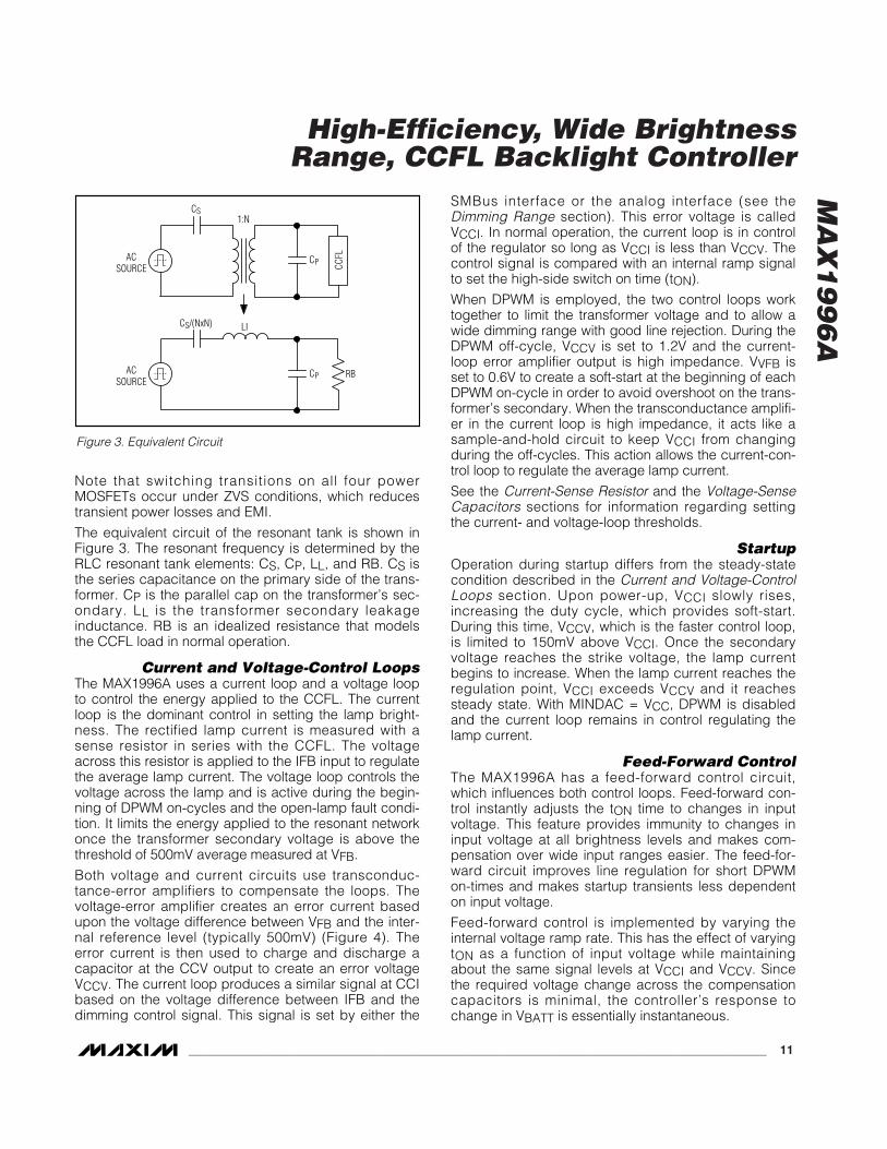
The equivalent circuit of the resonant tank is shown inFigure 3. The resonant frequency is determined by theRLC resonant tank elements: CS, CP, LL, and RB. CS isthe series capacitance on the primary side of the trans-former. CP is the parallel cap on the transformer’s sec-ondary. LL is the transformer secondary leakageinductance. RB is an idealized resistance that modelsthe CCFL load in normal operation.
Current and Voltage-Control LoopsThe MAX1996A uses a current loop and a voltage loopto control the energy applied to the CCFL. The currentloop is the dominant control in setting the lamp bright-ness. The rectified lamp current is measured with asense resistor in series with the CCFL. The voltageacross this resistor is applied to the IFB input to regulatethe average lamp current. The voltage loop controls thevoltage across the lamp and is active during the begin-ning of DPWM on-cycles and the open-lamp fault condi-tion. It limits the energy applied to the resonant networkonce the transformer secondary voltage is above thethreshold of 500mV average measured at VFB.
Both voltage and current circuits use transconduc-tance-error amplifiers to compensate the loops. Thevoltage-error amplifier creates an error current basedupon the voltage difference between VFB and the inter-nal reference level (typically 500mV) (Figure 4). Theerror current is then used to charge and discharge acapacitor at the CCV output to create an error voltageVCCV. The current loop produces a similar signal at CCIbased on the voltage difference between IFB and thedimming control signal. This signal is set by either the
SMBus interface or the analog interface (see theDimming Range section). This error voltage is calledVCCI. In normal operation, the current loop is in controlof the regulator so long as VCCI is less than VCCV. Thecontrol signal is compared with an internal ramp signalto set the high-side switch on time (tON).
When DPWM is employed, the two control loops worktogether to limit the transformer voltage and to allow awide dimming range with good line rejection. During theDPWM off-cycle, VCCV is set to 1.2V and the current-loop error amplifier output is high impedance. VVFB isset to 0.6V to create a soft-start at the beginning of eachDPWM on-cycle in order to avoid overshoot on the trans-former’s secondary. When the transconductance amplifi-er in the current loop is high impedance, it acts like asample-and-hold circuit to keep VCCI from changingduring the off-cycles. This action allows the current-con-trol loop to regulate the average lamp current.
See the Current-Sense Resistor and the Voltage-SenseCapacitors sections for information regarding settingthe current- and voltage-loop thresholds.
StartupOperation during startup differs from the steady-statecondition described in the Current and Voltage-ControlLoops section. Upon power-up, VCCI slowly rises,increasing the duty cycle, which provides soft-start.During this time, VCCV, which is the faster control loop,is limited to 150mV above VCCI. Once the secondaryvoltage reaches the strike voltage, the lamp currentbegins to increase. When the lamp current reaches theregulation point, VCCI exceeds VCCV and it reachessteady state. With MINDAC = VCC, DPWM is disabledand the current loop remains in control regulating thelamp current.
Feed-Forward ControlThe MAX1996A has a feed-forward control circuit,which influences both control loops. Feed-forward con-trol instantly adjusts the tON time to changes in inputvoltage. This feature provides immunity to changes ininput voltage at all brightness levels and makes com-pensation over wide input ranges easier. The feed-for-ward circuit improves line regulation for short DPWMon-times and makes startup transients less dependenton input voltage.
Feed-forward control is implemented by varying theinternal voltage ramp rate. This has the effect of varyingtON as a function of input voltage while maintainingabout the same signal levels at VCCI and VCCV. Sincethe required voltage change across the compensationcapacitors is minimal, the controller’s response tochange in VBATT is essentially instantaneous.
Figure 3. Equivalent Circuit
LI
RB
ACSOURCE
ACSOURCE
CCFL
1:NCS
CP
CP
CS/(NxN)

MA
X1
99
6A
High-Efficiency, Wide Brightness Range, CCFL Backlight Controller
12 ______________________________________________________________________________________
Transient Overvoltage Protection from Dropout
The MAX1996A is designed to maintain tight control ofthe transformer secondary under all transient conditionsincluding dropout. To maximize run time, it is desirableto allow the circuit to operate in dropout at extremelylow battery voltages where the backlight’s performanceis not critical. When VBATT is very low, the controllercan lose regulation and run at maximum duty cycle.Under these circumstances, a transient overvoltagecondition can occur when the AC adapter is suddenlyapplied to power the circuit. The feed-forward circuitryminimizes variations in lamp voltage due to such inputvoltage steps. The regulator also clamps the voltage onVCCI. Both features ensure that overvoltage transients
do not appear on the transformer when leavingdropout.
The VCCI clamp is unique in that it limits at the peaks ofthe voltage-ramp generator. As the circuit reachesdropout, VCCI approaches the peaks of the ramp gener-ator in order to reach maximum tON. If VBATT decreasesfurther, the control loop loses regulation and VCCI tries toreach its positive supply rail. The clamp on VCCI pre-vents this from happening and VCCI rides just above thepeaks of the PWM ramp. If VBATT continues to decrease,the feed-forward PWM ramp generator loses amplitudeand the clamp drags VCCI down with it to a voltagebelow where VCCI would have been if the circuit were notin dropout. When VBATT suddenly steps out of dropout,VCCI is still low and the MAX1996A maintains the driveon the transformer at the old dropout level. The control
BST1
BST2
GH1
LX1
GH2
LX2
GL1
GL2
PGND
CCFL
SH/SUS
MINDAC
CRF/SDA
CTL/SCL
MODE
CCV
VFB
CCI
IFB
LX2
LX1
ILMIT
GND
REF
BATT
VCC
REFSUPPLY
0.15V
0.5V
GMV
GMI
4mV
GND
VDD
DPWMOSC
LAMP CURRENT ANDDPWM CONTROL
SMBus
DPWMCOMP
PWM COMP
MINDAC = VCCY = 1, N =0
RAMPGENERATOR
IMIN COMP
IMAX COMP
CONTROLLOGIC
PEAKDETECTOR
PK_DETCLAMP
CCVCLAMP
MUX
MAX1996A
REFERENCEINPUT
CONTROLINPUT
INPUTVOLTAGE
Figure 4. Functional Diagram
MA
X1
99
6A
High-Efficiency, Wide Brightness Range, CCFL Backlight Controller
______________________________________________________________________________________ 13
loop then slowly corrects the lamp current by increasingVCCI, which brings the circuit back into regulation.
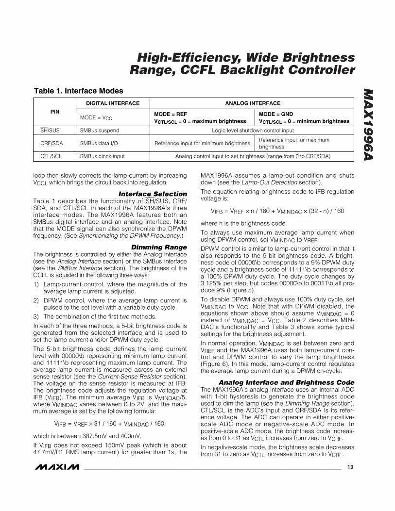
Interface SelectionTable 1 describes the functionality of SH/SUS, CRF/SDA, and CTL/SCL in each of the MAX1996A’s threeinterface modes. The MAX1996A features both anSMBus digital interface and an analog interface. Notethat the MODE signal can also synchronize the DPWMfrequency. (See Synchronizing the DPWM Frequency.)
Dimming RangeThe brightness is controlled by either the Analog Interface(see the Analog Interface section) or the SMBus Interface(see the SMBus Interface section). The brightness of theCCFL is adjusted in the following three ways:
1) Lamp-current control, where the magnitude of theaverage lamp current is adjusted.
2) DPWM control, where the average lamp current ispulsed to the set level with a variable duty cycle.
3) The combination of the first two methods.
In each of the three methods, a 5-bit brightness code isgenerated from the selected interface and is used toset the lamp current and/or DPWM duty cycle.
The 5-bit brightness code defines the lamp currentlevel with 00000\b representing minimum lamp currentand 11111\b representing maximum lamp current. Theaverage lamp current is measured across an externalsense resistor (see the Current-Sense Resistor section).The voltage on the sense resistor is measured at IFB.The brightness code adjusts the regulation voltage atIFB (VIFB). The minimum average VIFB is VMINDAC/5,where VMINDAC varies between 0 to 2V, and the maxi-mum average is set by the following formula:
VIFB = VREF 31 / 160 + VMINDAC / 160,
which is between 387.5mV and 400mV.
If VIFB does not exceed 150mV peak (which is about47.7mV/R1 RMS lamp current) for greater than 1s, the
MAX1996A assumes a lamp-out condition and shutsdown (see the Lamp-Out Detection section).
The equation relating brightness code to IFB regulationvoltage is:
VIFB = VREF n / 160 + VMINDAC (32 - n) / 160
where n is the brightness code.
To always use maximum average lamp current whenusing DPWM control, set VMINDAC to VREF.
DPWM control is similar to lamp-current control in that italso responds to the 5-bit brightness code. A bright-ness code of 00000\b corresponds to a 9% DPWM dutycycle and a brightness code of 11111\b corresponds toa 100% DPWM duty cycle. The duty cycle changes by3.125% per step, but codes 00000\b to 00011\b all pro-duce 9% (Figure 5).
To disable DPWM and always use 100% duty cycle, setVMINDAC to VCC. Note that with DPWM disabled, theequations shown above should assume VMINDAC = 0instead of VMINDAC = VCC. Table 2 describes MIN-DAC’s functionality and Table 3 shows some typicalsettings for the brightness adjustment.
In normal operation, VMINDAC is set between zero andVREF and the MAX1996A uses both lamp-current con-trol and DPWM control to vary the lamp brightness(Figure 6). In this mode, lamp-current control regulatesthe average lamp current during a DPWM on-cycle.
Analog Interface and Brightness CodeThe MAX1996A’s analog interface uses an internal ADCwith 1-bit hysteresis to generate the brightness codeused to dim the lamp (see the Dimming Range section).CTL/SCL is the ADC’s input and CRF/SDA is its refer-ence voltage. The ADC can operate in either positive-scale ADC mode or negative-scale ADC mode. Inpositive-scale ADC mode, the brightness code increas-es from 0 to 31 as VCTL increases from zero to VCRF.
In negative-scale mode, the brightness scale decreasesfrom 31 to zero as VCTL increases from zero to VCRF.
Table 1. Interface Modes
DIGITAL INTERFACE ANALOG INTERFACE
PINMODE = VCC
MODE = REFVCTL/SCL = 0 = maximum brightness
MODE = GNDVCTL/SCL = 0 = minimum brightness
SH/SUS SMBus suspend Logic level shutdown control input
CRF/SDA SMBus data I/O Reference input for minimum brightnessReference input for maximumbrightness
CTL/SCL SMBus clock input Analog control input to set brightness (range from 0 to CRF/SDA)

MA
X1
99
6A
High-Efficiency, Wide Brightness Range, CCFL Backlight Controller
14 ______________________________________________________________________________________
Figure 6. Combined Power Level
0
10
20
30
60
70
40
50
80
90
100
0 124 8 2016 24 28 32BRIGHTNESS CODE
COM
BINE
D PO
WER
LEV
EL (%
)
COMBINED POWER LEVEL (BOTHDPWM AND LAMP-CONTROL CURRENT)
Figure 5. DPWM Settings
0
10
20
30
60
70
40
50
80
90
100
0 124 8 2016 24 28 32BRIGHTNESS CODE
DPW
M D
UTY
CYCL
E (%
)
DPWM SETTINGS
Table 2. MINDAC FunctionalityCONDITION FUNCTION
MINDAC = VCCDPWM disabled (always on 100% duty cycle). Operates in lamp-current control only.(Use VMINDAC = 0 in the equations.)
MINDAC = REFDPWM control enabled, duty cycle ranges from 9% to 100%.Lamp-current control is disabled (always maximum current).
0 ≤ VMINDAC < VREF The device uses both lamp-current control and DPWM.
Table 3. Brightness Adjustment Ranges
RANGEPOSITIVE-SCALE
ADC MODENEGATIVE-SCALE
ADC MODESMBus
DACOUTPUT
DPWMDUTY
CYCLE (%)
COMBINEDPOWER
LEVEL (%)
MaximumBrightness
MODE = GND,VCRF/SDA =VCTL/SCL
MODE = REF,VCRF/SDA = 0
Bright [4:0] = 11111Full-scaleDAC output =387.5mV
100 100
MinimumBrightness
MODE = GND,VCRF/SDA = 0,VMINDAC = 1/3VREF
MODE = REF,VCRF/SDA = VCTL/SCL,VMINDAC = 1/3VREF
Bright [4:0] = 00000VMINDAC = 1/3VREF
Zero-scaleDAC output =VMINDAC/5
9 3
Note: The current level range is solely determined by the MINDAC to REF ratio and is externally set.
MA
X1
99
6A
High-Efficiency, Wide Brightness Range, CCFL Backlight Controller
______________________________________________________________________________________ 15
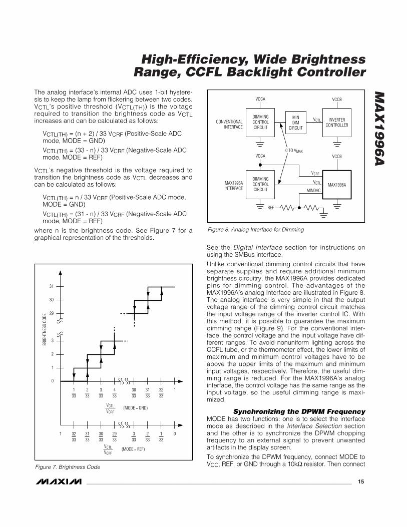
The analog interface’s internal ADC uses 1-bit hystere-sis to keep the lamp from flickering between two codes.VCTL’s positive threshold (VCTL(TH)) is the voltagerequired to transition the brightness code as VCTLincreases and can be calculated as follows:
VCTL(TH) = (n + 2) / 33 VCRF (Positive-Scale ADCmode, MODE = GND)
VCTL(TH) = (33 - n) / 33 VCRF (Negative-Scale ADCmode, MODE = REF)
VCTL’s negative threshold is the voltage required totransition the brightness code as VCTL decreases andcan be calculated as follows:
VCTL(TH) = n / 33 VCRF (Positive-Scale ADC mode, MODE = GND)
VCTL(TH) = (31 - n) / 33 VCRF (Negative-Scale ADC mode, MODE = REF)
where n is the brightness code. See Figure 7 for agraphical representation of the thresholds.
See the Digital Interface section for instructions onusing the SMBus interface.
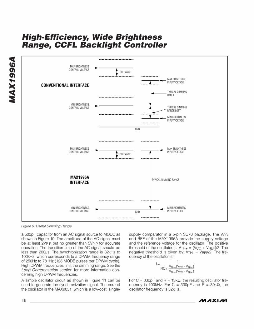
Unlike conventional dimming control circuits that haveseparate supplies and require additional minimumbrightness circuitry, the MAX1996A provides dedicatedpins for dimming control. The advantages of theMAX1996A’s analog interface are illustrated in Figure 8.The analog interface is very simple in that the outputvoltage range of the dimming control circuit matchesthe input voltage range of the inverter control IC. Withthis method, it is possible to guarantee the maximumdimming range (Figure 9). For the conventional inter-face, the control voltage and the input voltage have dif-ferent ranges. To avoid nonuniform lighting across theCCFL tube, or the thermometer effect, the lower limits ofmaximum and minimum control voltages have to beabove the upper limits of the maximum and minimuminput voltages, respectively. Therefore, the useful dim-ming range is reduced. For the MAX1996A’s analoginterface, the control voltage has the same range as theinput voltage, so the useful dimming range is maxi-mized.
Synchronizing the DPWM FrequencyMODE has two functions: one is to select the interfacemode as described in the Interface Selection sectionand the other is to synchronize the DPWM choppingfrequency to an external signal to prevent unwantedartifacts in the display screen.
To synchronize the DPWM frequency, connect MODE toVCC, REF, or GND through a 10kΩ resistor. Then connectFigure 7. Brightness Code
BRIG
HTNE
SS C
ODE
31
30
29
3
2
1
0
133
233
333
433
VCTLVCRF
(MODE = GND)
VCTLVCRF
(MODE = REF)
3033
3133
3233
1
3233
3133
3033
2933
333
233
133
01
Figure 8. Analog Interface for Dimming
0 TO VMAX
DIMMINGCONTROLCIRCUIT
VCCA
INVERTERCONTROLLER
VCCB
MINDIM
CIRCUIT
MAX1996A
VCTL
VCTL
MINDAC
VCRF
REF
CONVENTIONALINTERFACE
MAX1996AINTERFACE
DIMMINGCONTROLCIRCUIT
VCCA VCCB
MA
X1
99
6A
High-Efficiency, Wide Brightness Range, CCFL Backlight Controller
16 ______________________________________________________________________________________
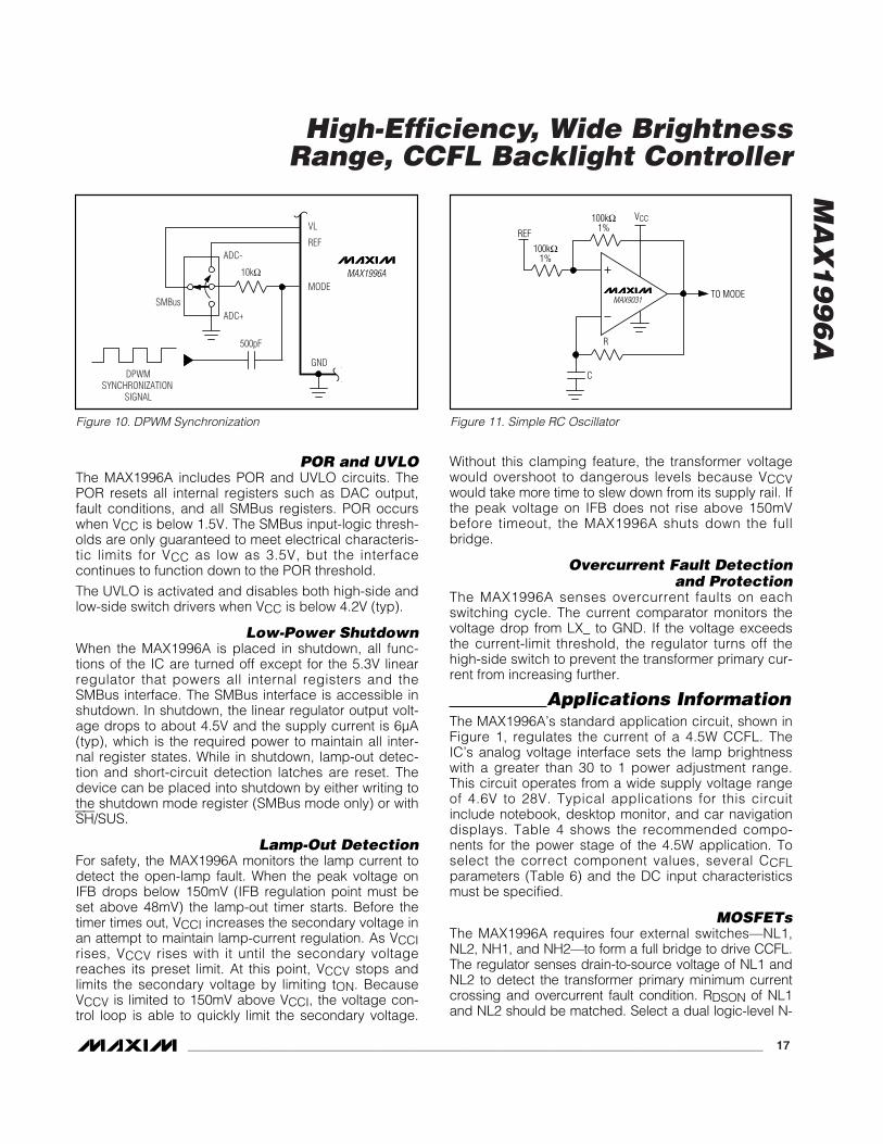
a 500pF capacitor from an AC signal source to MODE asshown in Figure 10. The amplitude of the AC signal mustbe at least 2VP-P but no greater than 5VP-P for accurateoperation. The transition time of the AC signal should beless than 200µs. The synchronization range is 32kHz to100kHz, which corresponds to a DPWM frequency rangeof 250Hz to 781Hz (128 MODE pulses per DPWM cycle).High DPWM frequencies limit the dimming range. See theLoop Compensation section for more information con-cerning high DPWM frequencies.
A simple oscillator circuit as shown in Figure 11 can beused to generate the synchronization signal. The core ofthe oscillator is the MAX9031, which is a low-cost, single-
supply comparator in a 5-pin SC70 package. The VCCand REF of the MAX1996A provide the supply voltageand the reference voltage for the oscillator. The positivethreshold of the oscillator is: VTH+ = (VCC + VREF)/2. Thenegative threshold is given by: VTH- = VREF/2. The fre-quency of the oscillator is:
For C = 330pF and R = 13kΩ, the resulting oscillator fre-quency is 100kHz. For C = 330pF and R = 39kΩ, theoscillator frequency is 32kHz.
fRC
V V VV V V
TH CC TH
TH CC TH
=+ − −
− − +
1
ln( )( )
Figure 9. Useful Dimming Range
GND
GND
MAX BRIGHTNESSCONTROL VOLTAGE
TOLERANCE
MIN BRIGHTNESSCONTROL VOLTAGE
MAX BRIGHTNESSINPUT VOLTAGE
MIN BRIGHTNESSINPUT VOLTAGE
MAX BRIGHTNESSCONTROL VOLTAGE
TOLERANCE
MIN BRIGHTNESSCONTROL VOLTAGE
MAX BRIGHTNESSINPUT VOLTAGE
MIN BRIGHTNESSINPUT VOLTAGE
TYPICAL DIMMINGRANGE
TYPICAL DIMMING RANGE
TYPICAL DIMMINGRANGE LOST
CONVENTIONAL INTERFACE
MAX1996AINTERFACE
MA
X1
99
6A
High-Efficiency, Wide Brightness Range, CCFL Backlight Controller
______________________________________________________________________________________ 17
POR and UVLOThe MAX1996A includes POR and UVLO circuits. ThePOR resets all internal registers such as DAC output,fault conditions, and all SMBus registers. POR occurswhen VCC is below 1.5V. The SMBus input-logic thresh-olds are only guaranteed to meet electrical characteris-tic limits for VCC as low as 3.5V, but the interfacecontinues to function down to the POR threshold.
The UVLO is activated and disables both high-side andlow-side switch drivers when VCC is below 4.2V (typ).
Low-Power ShutdownWhen the MAX1996A is placed in shutdown, all func-tions of the IC are turned off except for the 5.3V linearregulator that powers all internal registers and theSMBus interface. The SMBus interface is accessible inshutdown. In shutdown, the linear regulator output volt-age drops to about 4.5V and the supply current is 6µA(typ), which is the required power to maintain all inter-nal register states. While in shutdown, lamp-out detec-tion and short-circuit detection latches are reset. Thedevice can be placed into shutdown by either writing tothe shutdown mode register (SMBus mode only) or withSH/SUS.
Lamp-Out DetectionFor safety, the MAX1996A monitors the lamp current todetect the open-lamp fault. When the peak voltage onIFB drops below 150mV (IFB regulation point must beset above 48mV) the lamp-out timer starts. Before thetimer times out, VCCI increases the secondary voltage inan attempt to maintain lamp-current regulation. As VCCIrises, VCCV rises with it until the secondary voltagereaches its preset limit. At this point, VCCV stops andlimits the secondary voltage by limiting tON. BecauseVCCV is limited to 150mV above VCCI, the voltage con-trol loop is able to quickly limit the secondary voltage.
Without this clamping feature, the transformer voltagewould overshoot to dangerous levels because VCCVwould take more time to slew down from its supply rail. Ifthe peak voltage on IFB does not rise above 150mVbefore timeout, the MAX1996A shuts down the fullbridge.
Overcurrent Fault Detection and Protection
The MAX1996A senses overcurrent faults on eachswitching cycle. The current comparator monitors thevoltage drop from LX_ to GND. If the voltage exceedsthe current-limit threshold, the regulator turns off thehigh-side switch to prevent the transformer primary cur-rent from increasing further.
Applications InformationThe MAX1996A’s standard application circuit, shown inFigure 1, regulates the current of a 4.5W CCFL. TheIC’s analog voltage interface sets the lamp brightnesswith a greater than 30 to 1 power adjustment range.This circuit operates from a wide supply voltage rangeof 4.6V to 28V. Typical applications for this circuitinclude notebook, desktop monitor, and car navigationdisplays. Table 4 shows the recommended compo-nents for the power stage of the 4.5W application. Toselect the correct component values, several CCFLparameters (Table 6) and the DC input characteristicsmust be specified.
MOSFETsThe MAX1996A requires four external switches—NL1,NL2, NH1, and NH2—to form a full bridge to drive CCFL.The regulator senses drain-to-source voltage of NL1 andNL2 to detect the transformer primary minimum currentcrossing and overcurrent fault condition. RDSON of NL1and NL2 should be matched. Select a dual logic-level N-
Figure 10. DPWM Synchronization
MODE
GNDDPWM
SYNCHRONIZATION SIGNAL
10kΩ
500pF
ADC-
ADC+SMBus
VL
REF
MAX1996A
Figure 11. Simple RC Oscillator
TO MODE
100kΩ1%
100kΩ1%
R
C
REF
VCC
MAX9031

MA
X1
99
6A
High-Efficiency, Wide Brightness Range, CCFL Backlight Controller
18 ______________________________________________________________________________________
channel MOSFET with low RDSON to minimize conductionloss for NL1/NL2 and NH1/NH2 (Fairchild FDC6561). Theregulator softly turns on each of four switches in the fullbridge. ZVS occurs when the external power MOSFETsare turned on while their respective drain-to-source volt-ages are near zero volts. ZVS effectively eliminates theMOSFET transition losses caused by CRSS (drain-to-
source capacitance) and parasitic capacitance dis-charge. ZVS improves efficiency and reduces switch-ing-related EMI.
Current-Sense ResistorThe MAX1996A regulates the CCFL average currentthrough sense resistor R1 in Figure 1. The voltage at
Table 4. Components for the Standard Application Circuit
DESIGNATION DESCRIPTION RECOMMENDED DEVICE MANUFACTURER
TMK325BJ475MNTaiyo Yudenwww.t-yuden.com
C1 4.7µF, 25V X5R ceramic capacitor
C3225X7R1E475MTDKwww.tdk.com
C2 1µF, 25V X7R ceramic capacitorTMK316BJ105KLC3216X7R1E105K
Taiyo YudenTDK
GHM1038-SL-150J-3KMuratawww.murata.comC3
15pF, 3.1kV high-voltage ceramiccapacitor
C4520C0G3F150K TDK
EMK105BJ153KV Taiyo YudenC4 0.015µF, 16V X7R ceramic capacitor
GRM36X7R153K016 Murata
LMK105BJ104MV Taiyo Yuden
GRM36X5R104K010 MurataC5–C8, C10 0.1µF,10V X5R ceramic capacitors
C10055R1A104K TDK
C9 0.01µF, 16V X7R ceramic capacitor ECJ-0EB1C103KPanasonicwww.panasonic.com
MMBD4148SEFairchild Semiconductorwww.fairchildsemi.com
MMBD7000General Semiconductorwww.gensemi.com
D1 100mA dual-series diode
CMPD7000Central Semiconductorwww.centralsemi.com
BAT54AWDiodes Incorporatedwww.diodes.comD2
100mA dual Schottkydiode common anode
CMSSH-3A Central Semiconductor
FDC6561AN Fairchild SemiconductorNH1/NL1,NH2/NL2
Dual N-channel MOSFETs(30V, 0.095Ω, SOT23-6) TPC6201
Toshibawww.toshiba.com
R1 150Ω ±1% resistor — —
R2 2kΩ ±5% resistor — —
R3 100kΩ ±1% resistor — —
R4 49.9kΩ ±1% resistor — —
T1 1:100 transformer T912MG-1018Tokowww.tokoam.com

MA
X1
99
6A
High-Efficiency, Wide Brightness Range, CCFL Backlight Controller
______________________________________________________________________________________ 19
IFB is the half-wave rectified representation of the cur-rent through the lamp. The inverter regulates the aver-age voltage at IFB, which is controlled by either theanalog interface or the SMBus interface. To set themaximum lamp RMS current, determine R1 as follows:R1 = 0.444V/ICCFL, RMS, MAX, where ICCFL, RMS, MAXis the maximum RMS lamp current. MINDAC and thewave shape influence the actual maximum RMS lampcurrent. If necessary, use an RMS current meter tomake final adjustments to R1.
Voltage-Sense CapacitorsThe MAX1996A limits the transformer secondary voltageduring open-lamp fault through the capacitive dividerC3/C4. The voltage of VFB is proportional to CCFL volt-age. To set the maximum RMS secondary transformervoltage, choose C3 around 10pF to 22pF, and select C4such that C4 = VT(MAX)/1.11V C3, where VT(MAX) com-prises the maximum RMS secondary transformer voltage(above the strike voltage). R2 sets the VFB DC bias pointto zero volts. Choose R2 =10/(C4 6.28 FSW), whereFSW is the nominal resonant operating frequency.
Loop CompensationCCI sets the speed of the current loop that is used dur-ing startup, maintaining lamp-current regulation, andduring transients, caused by changing the lamp-cur-rent settling. The typical CCI capacitor value is 0.1µF.Larger values l imit lamp-current overshoot, butincrease setting time. Smaller values speed up itsresponse time, but extremely small values can lead toinstability.
CCV sets the speed of the voltage loop that affects start-up, DPWM transients, and operation in an open-tubefault condition. If DPWM is not used, the voltage controlloop should only be active during startup or an open-lamp fault. The CCV capacitors typical value is 0.01µF.Use the smallest value of CCV capacitor necessary toset an acceptable fault-transient response and not causeexcessive ringing at the beginning of a DPWM pulse.Larger CCV capacitor values reduce transient overshoot,but can degrade regulation at low DPWM duty cycles byincreasing the delay to strike voltage.
Resonant Components The MAX1996A works well with air-gap transformerswith turns ratio N in the order of NP:NS = 1:90 to 1:100for most applications. The transformer secondary reso-nant frequency must be controlled. A low-profile CCFLtransformer typically operates between 50kHz (Fmin)and 200kHz (Fmax). Transformer T1, DC blockingcapacitor C2, parallel capacitor C3, and the CCFLlamp form a resonant tank. The resonant frequency is
determined by the transformer secondary leakageinductance L, C2, and C3. The tank is a bandpass filterwhose lower frequency is bounded by L, N, and C2. Nis the transformer’s turns ratio. Choose C2 ≤ N2 (10
F2MIN L). The upper frequency is bounded by L andC3. Choose C3 ≥ 1/(40 F2MIN L).
Other ComponentsThe high-side MOSFET drivers (GH1 and GH2) arepowered by the external bootstrap circuit formed byD2, C5, and C6. Connect BST1/BST2 through a dualsignal-level Schottky diode D2 to VDD, and connect it toLX1/LX2 with 0.1µF ceramic capacitors. Use a dual-series signal-level diode (D1) to generate the half-waverectified current-sense voltage across R1. The currentthrough these diodes is the lamp current.
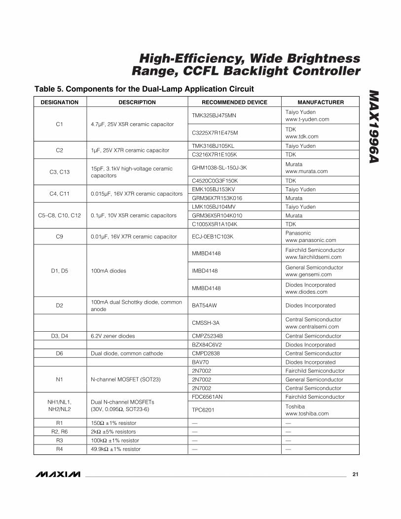
Dual-Lamp RegulatorThe MAX1996A can be used to drive two CCFL tubesas shown in Figure 12. See Table 5 for componentselection. The circuit consists of two identical trans-formers with primary windings connected in paralleland secondary windings in series. The two transform-ers can also be replaced with a single transformer,which has one primary winding and two secondarywindings. The advantage of the series secondary wind-ings is that the same current flows through both lamps,resulting in approximately the same brightness.
In normal operation, C12 is charged to approximately6V biasing N1 on, which permits current to flow in theloop as follows: in the first half cycle, current flowsthrough the secondary winding of T1, CCFL1, diodeD1, MOSFET N1, sense resistor R1, zener diode D4(forward bias), CCFL2, and finally returning to T2. In thesecond half cycle, the lamp current flows through T2,CCFL2, D4 (breakdown), D3 (forward bias), CCFL1,and back to T1.
The roundabout path of current flow is necessary inorder to detect an open-lamp condition when eitherCCFL is removed. If CCFL1 is open, the lamp currentcannot flow through sense resistor R1. When IFB dropsbelow 150mV, the controller detects the condition andshuts down after a 1s delay. During the delay, currentcan flow from T2 through CCFL2, D4 (breakdown), andR6 back to T2. If CCFL2 is removed, the voltage acrossD4 drops to zero and C11 is discharged through R5.N1 is biased off, which forces the voltage at IFB to dropto zero once again. During the 1s turn-off delay, currentflows from T1 to CCFL1 through D3 (breakdown) andR6 back to T1. D3 clamps the drain of N1 enabling theuse of a MOSFET with modest breakdown characteristics.

MA
X1
99
6A
High-Efficiency, Wide Brightness Range, CCFL Backlight Controller
20 ______________________________________________________________________________________
The secondary voltages of both transformers are moni-tored through the two identical capacitive voltage-dividers (C3/C4 and C13/C11). Dual-diode D6 rectifiesthe two sensed voltages and passes the signal to theVFB pin. A full-wave rectified sinusoidal waveformappears at the VFB pin. The RMS value of this new VFBsignal is greater than the half-wave rectified signal inthe single-lamp application. To compensate for thewaveform change and the forward-voltage drop in thediodes, the capacitive voltage-divider ratio must bedecreased. Choose C3 around 10pF to 22pF, andselect C4 according to C4 = VT, MAX/1.33V C3, whereVT, MAX is the maximum transformer secondary RMSvoltage.
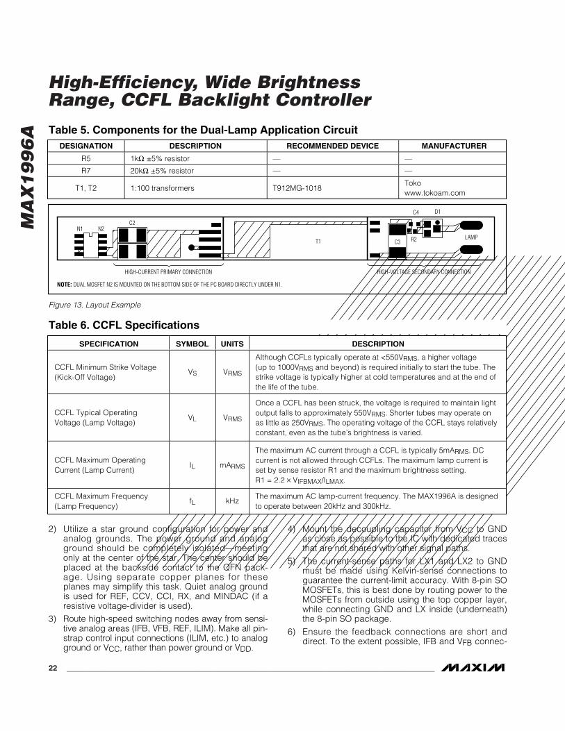
Layout GuidelinesCareful PC board layout is critical to achieve lowswitching losses and clean, stable operation. The high-voltage and switching-power stages require particularattention (Figure 13). The high-voltage sections of thelayout need to be well separated from the control cir-cuit. Most layouts are constrained to long narrow PCboards, so this separation occurs naturally.
Follow these guidelines for good PC board layout:1) Keep the high-current paths short and wide, espe-
cially at the ground terminals. This is essential forstable, jitter-free operation, and high efficiency.
Figure 12. Dual-Lamp Application Circuit
MAX1996A
REF ILIM
MIN
DAC
GND
MOD
E
CRF/
SDA
CTL/
SCL
GH2
LX2
BST2BST1
LX1
C3
C2T1
T2
C1
C6
ON/OFF
REFERENCE INPUT
CONTROL INPUT
R3
C10
C8
C7
C5
D2-1
C9
D2-2
GH1
GL1
VCC
BATT
CCV
CCI
IFB
VFB
GL2
PGND
VDD
SH/S
USNL1 NL2
NH1 NH2
C4
R4
C12
C11
C13D4
D5
D3D6
R6
N1
R2 R7
R6
R5
R1
D1
VIN5V TO 28V
CCFL
CCFL2
MA
X1
99
6A
High-Efficiency, Wide Brightness Range, CCFL Backlight Controller
______________________________________________________________________________________ 21
Table 5. Components for the Dual-Lamp Application Circuit
DESIGNATION DESCRIPTION RECOMMENDED DEVICE MANUFACTURER
TMK325BJ475MNTaiyo Yudenwww.t-yuden.com
C1 4.7µF, 25V X5R ceramic capacitor
C3225X7R1E475MTDKwww.tdk.com
TMK316BJ105KL Taiyo YudenC2 1µF, 25V X7R ceramic capacitor
C3216X7R1E105K TDK
GHM1038-SL-150J-3KMuratawww.murata.comC3, C13
15pF, 3.1kV high-voltage ceramiccapacitors
C4520C0G3F150K TDK
EMK105BJ153KV Taiyo YudenC4, C11 0.015µF, 16V X7R ceramic capacitors
GRM36X7R153K016 Murata
LMK105BJ104MV Taiyo Yuden
GRM36X5R104K010 MurataC5–C8, C10, C12 0.1µF, 10V X5R ceramic capacitors
C1005X5R1A104K TDK
C9 0.01µF, 16V X7R ceramic capacitor ECJ-0EB1C103KPanasonicwww.panasonic.com
MMBD4148Fairchild Semiconductorwww.fairchildsemi.com
IMBD4148General Semiconductorwww.gensemi.com
D1, D5 100mA diodes
MMBD4148Diodes Incorporatedwww.diodes.com
D2100mA dual Schottky diode, commonanode
BAT54AW Diodes Incorporated
CMSSH-3ACentral Semiconductorwww.centralsemi.com
D3, D4 6.2V zener diodes CMPZ5234B Central Semiconductor
BZX84C6V2 Diodes Incorporated
D6 Dual diode, common cathode CMPD2838 Central Semiconductor
BAV70 Diodes Incorporated
2N7002 Fairchild Semiconductor
2N7002 General SemiconductorN1 N-channel MOSFET (SOT23)
2N7002 Central Semiconductor
FDC6561AN Fairchild SemiconductorNH1/NL1,NH2/NL2
Dual N-channel MOSFETs(30V, 0.095Ω, SOT23-6) TPC6201
Toshibawww.toshiba.com
R1 150Ω ±1% resistor — —
R2, R6 2kΩ ±5% resistors — —
R3 100kΩ ±1% resistor — —
R4 49.9kΩ ±1% resistor — —
MA
X1
99
6A
High-Efficiency, Wide Brightness Range, CCFL Backlight Controller
22 ______________________________________________________________________________________
2) Utilize a star ground configuration for power andanalog grounds. The power ground and analogground should be completely isolated—meetingonly at the center of the star. The center should beplaced at the backside contact to the QFN pack-age. Using separate copper planes for theseplanes may simplify this task. Quiet analog groundis used for REF, CCV, CCI, RX, and MINDAC (if aresistive voltage-divider is used).
3) Route high-speed switching nodes away from sensi-tive analog areas (IFB, VFB, REF, ILIM). Make all pin-strap control input connections (ILIM, etc.) to analogground or VCC, rather than power ground or VDD.
4) Mount the decoupling capacitor from VCC to GNDas close as possible to the IC with dedicated tracesthat are not shared with other signal paths.
5) The current-sense paths for LX1 and LX2 to GNDmust be made using Kelvin-sense connections toguarantee the current-limit accuracy. With 8-pin SOMOSFETs, this is best done by routing power to theMOSFETs from outside using the top copper layer,while connecting GND and LX inside (underneath)the 8-pin SO package.
6) Ensure the feedback connections are short anddirect. To the extent possible, IFB and VFB connec-
Figure 13. Layout Example
NOTE: DUAL MOSFET N2 IS MOUNTED ON THE BOTTOM SIDE OF THE PC BOARD DIRECTLY UNDER N1.
HIGH-CURRENT PRIMARY CONNECTION HIGH-VOLTAGE SECONDARY CONNECTION
LAMPN1 N2
T1
C4
C2
D1
R2C3
Table 6. CCFL Specifications
SPECIFICATION SYMBOL UNITS DESCRIPTION
CCFL Minimum Strike Voltage(Kick-Off Voltage)
VS VRMS
Although CCFLs typically operate at <550VRMS, a higher voltage(up to 1000VRMS and beyond) is required initially to start the tube. Thestrike voltage is typically higher at cold temperatures and at the end ofthe life of the tube.
CCFL Typical OperatingVoltage (Lamp Voltage)
VL VRMS
Once a CCFL has been struck, the voltage is required to maintain lightoutput falls to approximately 550VRMS. Shorter tubes may operate onas little as 250VRMS. The operating voltage of the CCFL stays relativelyconstant, even as the tube’s brightness is varied.
CCFL Maximum OperatingCurrent (Lamp Current)
IL mARMS
The maximum AC current through a CCFL is typically 5mARMS. DCcurrent is not allowed through CCFLs. The maximum lamp current isset by sense resistor R1 and the maximum brightness setting.R1 = 2.2 VIFBMAX/ILMAX.
CCFL Maximum Frequency(Lamp Frequency)
fL kHzThe maximum AC lamp-current frequency. The MAX1996A is designedto operate between 20kHz and 300kHz.
Table 5. Components for the Dual-Lamp Application CircuitDESIGNATION DESCRIPTION RECOMMENDED DEVICE MANUFACTURER
R5 1kΩ ±5% resistor — —
R7 20kΩ ±5% resistor — —
T1, T2 1:100 transformers T912MG-1018Tokowww.tokoam.com
MA
X1
99
6A
High-Efficiency, Wide Brightness Range, CCFL Backlight Controller
______________________________________________________________________________________ 23
tions should be far away from the high-voltagetraces and the transformer.
7) To the extent possible, high-voltage trace clearanceon the transformer’s secondary should be widelyseparated. The high-voltage traces should also beseparated from adjacent ground planes to preventcapacitive coupling losses.
8) The traces to the capacitive voltage-divider on thetransformer’s secondary need to be widely separat-ed to prevent arcing. Moving these traces to oppo-site sides of the board can be beneficial in somecases (Figure 13).
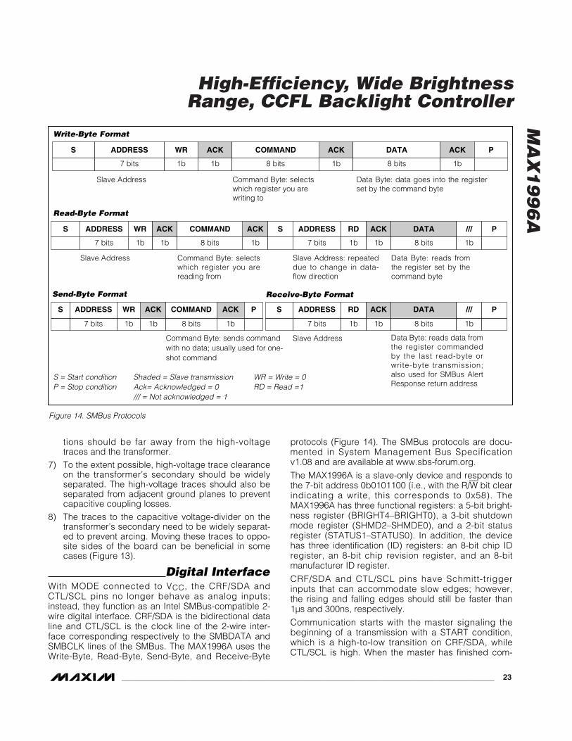
Digital InterfaceWith MODE connected to VCC, the CRF/SDA andCTL/SCL pins no longer behave as analog inputs;instead, they function as an Intel SMBus-compatible 2-wire digital interface. CRF/SDA is the bidirectional dataline and CTL/SCL is the clock line of the 2-wire inter-face corresponding respectively to the SMBDATA andSMBCLK lines of the SMBus. The MAX1996A uses theWrite-Byte, Read-Byte, Send-Byte, and Receive-Byte
protocols (Figure 14). The SMBus protocols are docu-mented in System Management Bus Specificationv1.08 and are available at www.sbs-forum.org.
The MAX1996A is a slave-only device and responds tothe 7-bit address 0b0101100 (i.e., with the R/W bit clearindicating a write, this corresponds to 0x58). TheMAX1996A has three functional registers: a 5-bit bright-ness register (BRIGHT4–BRIGHT0), a 3-bit shutdownmode register (SHMD2–SHMDE0), and a 2-bit statusregister (STATUS1–STATUS0). In addition, the devicehas three identification (ID) registers: an 8-bit chip IDregister, an 8-bit chip revision register, and an 8-bitmanufacturer ID register.
CRF/SDA and CTL/SCL pins have Schmitt-triggerinputs that can accommodate slow edges; however,the rising and falling edges should still be faster than1µs and 300ns, respectively.
Communication starts with the master signaling thebeginning of a transmission with a START condition,which is a high-to-low transition on CRF/SDA, whileCTL/SCL is high. When the master has finished com-
1b
ACK
1b7 bits
ADDRESS ACK
1b
WR
8 bits
DATA
1b
ACK P
8 bits
S COMMAND
Write-Byte Format
Receive-Byte Format
Slave Address Command Byte: selectswhich register you arewriting to
Data Byte: data goes into the registerset by the command byte
1b
ACK
1b7 bits
ADDRESS ACK
1b
WR S
1b
ACK
8 bits
DATA
7 bits
ADDRESS
1b
RD
1b8 bits
/// PS COMMAND
Slave Address
Slave AddressCommand Byte: sends commandwith no data; usually used for one-shot command
Command Byte: selectswhich register you arereading from
Slave Address: repeateddue to change in data-flow direction
Data Byte: reads fromthe register set by thecommand byte
1b
ACK
7 bits
ADDRESS
1b
RD
8 bits
DATA
1b
/// PS
Data Byte: reads data fromthe register commandedby the last read-byte orwrite-byte transmission;also used for SMBus AlertResponse return address
S = Start condition Shaded = Slave transmission WR = Write = 0P = Stop condition Ack= Acknowledged = 0 RD = Read =1
/// = Not acknowledged = 1
1b
ACK
7 bits
ADDRESS
1b
WR
8 bits
COMMAND
1b
ACK PS
Send-Byte Format
Read-Byte Format
Figure 14. SMBus Protocols

MA
X1
99
6A
High-Efficiency, Wide Brightness Range, CCFL Backlight Controller
24 ______________________________________________________________________________________
municating with the slave, the master issues a STOPcondition (P), which is low-to-high transition onCRF/SDA, while CTL/SCL is high. The bus is then freefor another transmission. Figures 15 and 16 show thetiming diagram for signals on the 2-wire interface. Theaddress-byte, command-byte, and data-byte are trans-mitted between the START and STOP conditions. TheCRF/SDA state is allowed to change only whileCTL/SCL is low, except for the START and STOP condi-tions. Data is transmitted in 8-bit words and is sampledon the rising edge of CTL/SCL. Nine clock cycles arerequired to transfer each byte in or out of theMAX1996A since either the master or the slaveacknowledges the receipt of the correct byte during theninth clock. If the MAX1996A receives its correct slaveaddress followed by R/W = 0, it expects to receive 1 or2 bytes of information (depending on the protocol). If
the device detects a START or STOP condition prior toclocking in the bytes of data, it considers this an errorcondition and disregards all the data. If the transmis-sion is completed correctly, the registers are updatedimmediately after a STOP (or RESTART) condition. Ifthe MAX1996A receives its correct slave address fol-lowed by R/W = 1, it expects to clock out the registerdata selected by the previous command byte.
SMBus CommandsThe MAX1996A registers are accessible through sever-al different redundant commands (i.e., the command-byte in the read-byte and write-byte protocols), whichcan be used to read or write the brightness, SHMD_,status, or ID registers.
Table 6 summarizes the command-byte’s registerassignments, as well as each register’s power-on state.
Figure 15. SMBus Write Timing
SMBCLK
A B C D E F G H I J K
SMBDATA
tSU:STA tHD:STA
tLOW tHIGH
tSU:DAT tHD:DATtHD:DAT tSU:STO tBUF
A = START CONDITIONB = MSB OF ADDRESS CLOCKED INTO SLAVEC = LSB OF ADDRESS CLOCKED INTO SLAVED = R/W BIT CLOCKED INTO SLAVEE = SLAVE PULLS SMBDATA LINE LOW
L M
F = ACKNOWLEDGE BIT CLOCKED INTO MASTERG = MSB OF DATA CLOCKED INTO SLAVE H = LSB OF DATA CLOCKED INTO SLAVEI = SLAVE PULLS SMBDATA LINE LOW
J = ACKNOWLEDGE CLOCKED INTO MASTERK = ACKNOWLEDGE CLOCK PULSEL = STOP CONDITION, DATA EXECUTED BY SLAVEM = NEW START CONDITION
Figure 16. SMBus Read Timing
SMBCLK
A = START CONDITIONB = MSB OF ADDRESS CLOCKED INTO SLAVEC = LSB OF ADDRESS CLOCKED INTO SLAVED = R/W BIT CLOCKED INTO SLAVE
A B C D E F G H I J
SMBDATA
tSU:STA tHD:STA
tLOW tHIGH
tSU:DAT tHD:DAT tSU:DAT tSU:STO tBUF
K
E = SLAVE PULLS SMBDATA LINE LOWF = ACKNOWLEDGE BIT CLOCKED INTO MASTERG = MSB OF DATA CLOCKED INTO MASTERH = LSB OF DATA CLOCKED INTO MASTER
I = ACKNOWLEDGE CLOCK PULSEJ = STOP CONDITIONK = NEW START CONDITION
MA
X1
99
6A
High-Efficiency, Wide Brightness Range, CCFL Backlight Controller
______________________________________________________________________________________ 25
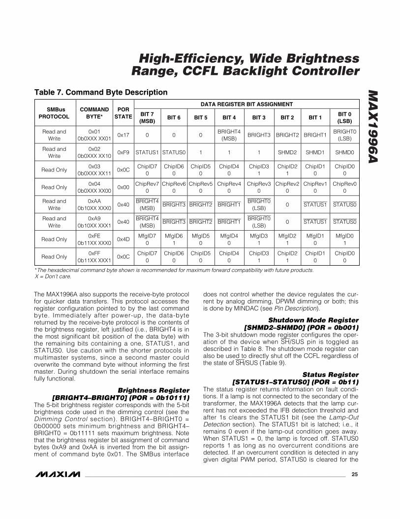
The MAX1996A also supports the receive-byte protocolfor quicker data transfers. This protocol accesses theregister configuration pointed to by the last commandbyte. Immediately after power-up, the data-bytereturned by the receive-byte protocol is the contents ofthe brightness register, left justified (i.e., BRIGHT4 is inthe most significant bit position of the data byte) withthe remaining bits containing a one, STATUS1, andSTATUS0. Use caution with the shorter protocols inmultimaster systems, since a second master couldoverwrite the command byte without informing the firstmaster. During shutdown the serial interface remainsfully functional.
Brightness Register [BRIGHT4–BRIGHT0] (POR = 0b10111)
The 5-bit brightness register corresponds with the 5-bitbrightness code used in the dimming control (see theDimming Control section). BRIGHT4–BRIGHT0 =0b00000 sets minimum brightness and BRIGHT4–BRIGHT0 = 0b11111 sets maximum brightness. Notethat the brightness register bit assignment of commandbytes 0xA9 and 0xAA is inverted from the bit assign-ment of command byte 0x01. The SMBus interface
does not control whether the device regulates the cur-rent by analog dimming, DPWM dimming or both; thisis done by MINDAC (see Pin Description).
Shutdown Mode Register [SHMD2–SHMD0] (POR = 0b001)
The 3-bit shutdown mode register configures the oper-ation of the device when SH/SUS pin is toggled asdescribed in Table 8. The shutdown mode register canalso be used to directly shut off the CCFL regardless ofthe state of SH/SUS (Table 9).
Status Register[STATUS1–STATUS0] (POR = 0b11)
The status register returns information on fault condi-tions. If a lamp is not connected to the secondary of thetransformer, the MAX1996A detects that the lamp cur-rent has not exceeded the IFB detection threshold andafter 1s clears the STATUS1 bit (see the Lamp-OutDetection section). The STATUS1 bit is latched; i.e., itremains 0 even if the lamp-out condition goes away.When STATUS1 = 0, the lamp is forced off. STATUS0reports 1 as long as no overcurrent conditions aredetected. If an overcurrent condition is detected in anygiven digital PWM period, STATUS0 is cleared for the
Table 7. Command Byte DescriptionDATA REGISTER BIT ASSIGNMENT
SMBusPROTOCOL
COMMANDBYTE*
PORSTATE BIT 7
(MSB)BIT 6 BIT 5 BIT 4 BIT 3 BIT 2 BIT 1
BIT 0(LSB)
Read andWrite
0x010b0XXX XX01
0x17 0 0 0BRIGHT4
(MSB)BRIGHT3 BRIGHT2 BRIGHT1
BRIGHT0(LSB)
Read andWrite
0x020b0XXX XX10
0xF9 STATUS1 STATUS0 1 1 1 SHMD2 SHMD1 SHMD0
Read Only0x03
0b0XXX XX110x0C
ChipID70
ChipID60
ChipID50
ChipID40
ChipID31
ChipID21
ChipID10
ChipID00
Read Only0x04
0b0XXX XX000x00
ChipRev70
ChipRev60
ChipRev50
ChipRev40
ChipRev30
ChipRev20
ChipRev10
ChipRev00
Read andWrite
0xAA0b10XX XXX0
0x40BRIGHT4
(MSB)BRIGHT3 BRIGHT2 BRIGHT1
BRIGHT0(LSB)
0 STATUS1 STATUS0
Read andWrite
0xA90b10XX XXX1
0x40BRIGHT4
(MSB)BRIGHT3 BRIGHT2 BRIGHT1
BRIGHT0(LSB)
0 STATUS1 STATUS0
Read Only0xFE
0b11XX XXX00x4D
MfgID70
MfgID61
MfgID50
MfgID40
MfgID31
MfgID21
MfgID10
MfgID01
Read Only0xFF
0b11XX XXX10x0C
ChipID70
ChipID60
ChipID50
ChipID40
ChipID31
ChipID21
ChipID10
ChipID00
*The hexadecimal command byte shown is recommended for maximum forward compatibility with future products. X = Don’t care.

MA
X1
99
6A
High-Efficiency, Wide Brightness Range, CCFL Backlight Controller
26 ______________________________________________________________________________________
duration of the following digital PWM period. If an over-current condition is not detected in any given digitalPWM period, STATUS0 is set for the duration of the fol-lowing digital PWM period. Forcing the CCFL lamp offby entering shutdown, writing to the mode register, orby toggling SHB/SUS sets STATUS1. Note that the sta-tus register bit assignment of command byte 0xA9 isinverted from the bit assignment of command byte 0x80.
ID RegistersThe ID registers return information on the manufacturer,the chip ID, and the chip revision number. TheMAX1996A is the first-generation advanced CCFL con-troller and its ChipRev is 0x00. Reading from MfgIDregister returns 0x4D, which is the ASCII code for M(for Maxim), the ChipID register returns 0x0C. Writing tothese registers has no effect.
Chip InformationTRANSISTOR COUNT: 7364
Table 8. SHMD Register Bit Descriptions
BIT NAMEPOR
STATEDESCRIPTION
2 SHMD2 0SHMD2 = 1 forces the lamp off and sets STATUS1. SHMD2 = 0 allows the lamp to operatealthough it may still be shut down by the /SH\/SUS pin (depending on the state of SHMD1and SHMD0).
1 SHMD1 0When SH/SUS = 0, this bit has no effect. SH/SUS = 1 and SHMD1 = 1 forces the lamp offand sets STATUS1. SH/SUS = 1 and SHMD1 = 0 allows the lamp to operate although itmay still be shut down by the SHMD2 bit.
0 SHMD0 1When SH/SUS = 1, this bit has no effect. SH/SUS = 0 and SHMD0 = 1 forces the lamp offand sets STATUS1. SH/SUS = 0 and SHMD0 = 0 allows the lamp to operate although itmay still be shut down by the SHMD2 bit.
Table 9. SH/SUS and SHMD Register Truth TableSH/SUS SHMD2 SHMD1 SHMD0 OPERATING MODE
0 0 X 0 Operate
0 0 X 1 Shutdown, STATUS1 set
1 0 0 X Operate
1 0 1 X Shutdown, STATUS1 set
X 1 X X Shutdown, STATUS1 set
X = Don’t care.
Table 10. Status Register Bit Descriptions (Read Only/Writes Have No Effect)
BIT NAMEPOR
STATEDESCRIPTION
1 STATUS1 1STATUS1 = zero means that a lamp-out condition has been detected. The STATUS1 bitstays clear even after the lamp-out condition has gone away. The only way to set STATUS1is to shut off the lamp by programming the mode register or by toggling SHB/SUS.
0 STATUS0 1STATUS0 = zero means that an overcurrent condition was detected during the previousdigital PWM period. STATUS0 = 1 means that no overcurrent condition was detectedduring the previous digital PWM period.

MA
X1
99
6A
High-Efficiency, Wide Brightness Range, CCFL Backlight Controller
______________________________________________________________________________________ 27
QFN
TH
IN 5
x5x0
.8 .E
PS
D2
(ND-1) X e
e
D
C
PIN # 1 I.D.
(NE-1) X e
E/2
E
0.08 C
0.10 C
A
A1 A3
DETAIL A
0.15 C B
0.15 C A
DOCUMENT CONTROL NO.
21-0140
PACKAGE OUTLINE16, 20, 28, 32L, QFN THIN, 5x5x0.8 mm
PROPRIETARY INFORMATION
APPROVAL
TITLE:
CREV.
21
E2/2
E2
0.10 M C A B
PIN # 1 I.D.
b
0.35x45
L
D/2D2/2
LC
LC
e e
LCCL
k
k
LL
22
21-0140REV.DOCUMENT CONTROL NO.APPROVAL
PROPRIETARY INFORMATION
TITLE:
COMMON DIMENSIONS EXPOSED PAD VARIATIONS
1. DIMENSIONING & TOLERANCING CONFORM TO ASME Y14.5M-1994.
2. ALL DIMENSIONS ARE IN MILLIMETERS. ANGLES ARE IN DEGREES.
3. N IS THE TOTAL NUMBER OF TERMINALS.
4. THE TERMINAL #1 IDENTIFIER AND TERMINAL NUMBERING CONVENTION SHALL CONFORM TO JESD 95-1 SPP-012. DETAILS OF TERMINAL #1 IDENTIFIER ARE OPTIONAL, BUT MUST BE LOCATED WITHIN THE ZONE INDICATED. THE TERMINAL #1 IDENTIFIER MAY BE EITHER A MOLD OR MARKED FEATURE.
5. DIMENSION b APPLIES TO METALLIZED TERMINAL AND IS MEASURED BETWEEN 0.25 mm AND 0.30 mm FROM TERMINAL TIP.
6. ND AND NE REFER TO THE NUMBER OF TERMINALS ON EACH D AND E SIDE RESPECTIVELY.
7. DEPOPULATION IS POSSIBLE IN A SYMMETRICAL FASHION.
8. COPLANARITY APPLIES TO THE EXPOSED HEAT SINK SLUG AS WELL AS THE TERMINALS.
9. DRAWING CONFORMS TO JEDEC MO220.
NOTES:
10. WARPAGE SHALL NOT EXCEED 0.10 mm.
C
PACKAGE OUTLINE16, 20, 28, 32L, QFN THIN, 5x5x0.8 mm
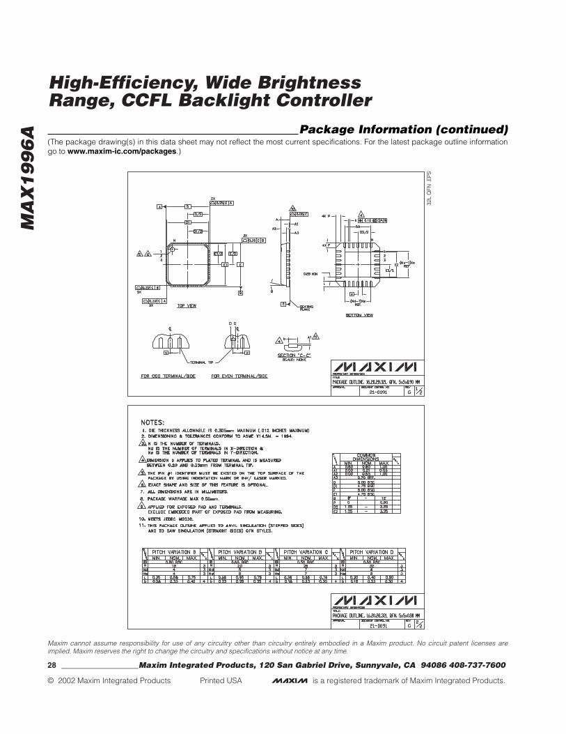
Package Information(The package drawing(s) in this data sheet may not reflect the most current specifications. For the latest package outline informationgo to www.maxim-ic.com/packages.)
MA
X1
99
6A
High-Efficiency, Wide Brightness Range, CCFL Backlight Controller
Maxim cannot assume responsibility for use of any circuitry other than circuitry entirely embodied in a Maxim product. No circuit patent licenses areimplied. Maxim reserves the right to change the circuitry and specifications without notice at any time.
28 ____________________Maxim Integrated Products, 120 San Gabriel Drive, Sunnyvale, CA 94086 408-737-7600
© 2002 Maxim Integrated Products Printed USA is a registered trademark of Maxim Integrated Products.
32L
QFN
.EP
S
Package Information (continued)(The package drawing(s) in this data sheet may not reflect the most current specifications. For the latest package outline informationgo to www.maxim-ic.com/packages.)