Embed Size (px)
Citation preview
Ping Gui, ProfessorDepartment of Electrical Engineering
Lyle School of EngineeringSouthern Methodist University
HEPIC 2017 @SLACOct. 4-6, 2017
IC Design at SMU EE Led by Ping Gui
[email protected] [email protected]
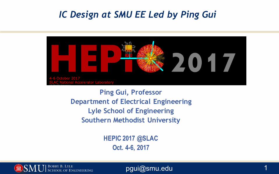
Ping Gui’s Research on IC Design
uAnalog, Mixed-signal and RF IC design for a variety of applications
uFunded by federal agencies, industry, foundations etc.
uCurrently 8 full-time Ph.D. students, several MS and undergraduate students
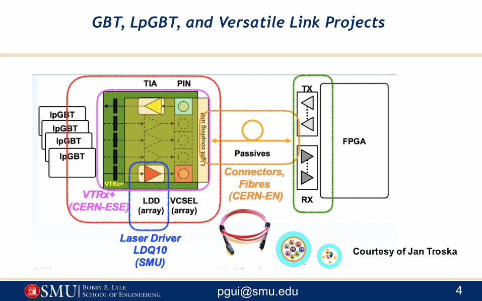
u ICs for HEP experiments u with CERN: GBT, LpGBT, Versatile Link
u Fermilab: COLDATA
u ICs for consumer electronics and communicationsu High-speed optical and wireline communicationsu 5G wireless and automotive radar
u ICs for Biomedical applications
Recent and On-going Research Projects
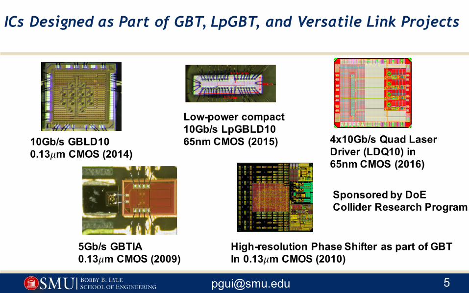
ICs Designed as Part of GBT, LpGBT, and Versatile Link Projects
10Gb/s GBLD10 0.13𝜇m CMOS (2014)
Low-power compact 10Gb/s LpGBLD10 65nm CMOS (2015) 4x10Gb/s Quad Laser
Driver (LDQ10) in65nm CMOS (2016)
5Gb/s GBTIA0.13𝜇m CMOS (2009)
High-resolution Phase Shifter as part of GBT In 0.13𝜇m CMOS (2010)
Sponsored by DoE Collider Research Program
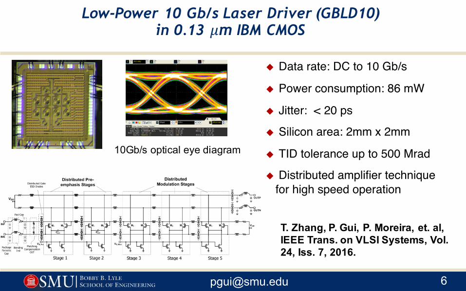
Low-Power 10 Gb/s Laser Driver (GBLD10) in 0.13 𝜇m IBM CMOS
u Data rate: DC to 10 Gb/s
u Power consumption: 86 mW
u Jitter: < 20 ps
u Silicon area: 2mm x 2mm
u TID tolerance up to 500 Mrad
u Distributed amplifier technique for high speed operation
T. Zhang, P. Gui, P. Moreira, et. al, IEEE Trans. on VLSI Systems, Vol. 24, Iss. 7, 2016.
10Gb/s optical eye diagram
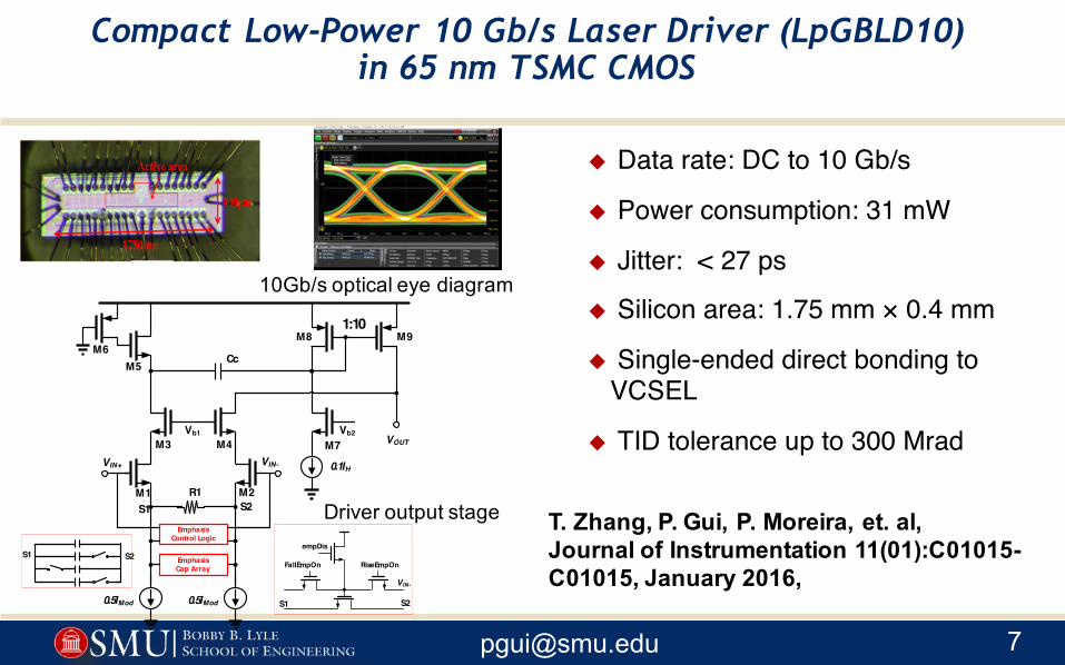
Compact Low-Power 10 Gb/s Laser Driver (LpGBLD10) in 65 nm TSMC CMOS
u Data rate: DC to 10 Gb/s
u Power consumption: 31 mW
u Jitter: < 27 ps
u Silicon area: 1.75 mm × 0.4 mm
u Single-ended direct bonding to VCSEL
u TID tolerance up to 300 Mrad
T. Zhang, P. Gui, P. Moreira, et. al, Journal of Instrumentation 11(01):C01015-C01015, January 2016,
VIN+
0.5IMod
M1 M2
VIN-
Emphasis Control Logic
Emphasis Cap Array
0.5IMod
R1
M3 M4Vb1 Vb2
0.1IH
empDis
VIN-
S1 S2
S1 S2
FallEmpOn RiseEmpOn
VOUT
M5M6
M7
M8 M9
Cc
S1 S2
1:10
10Gb/s optical eye diagram
Driver output stage
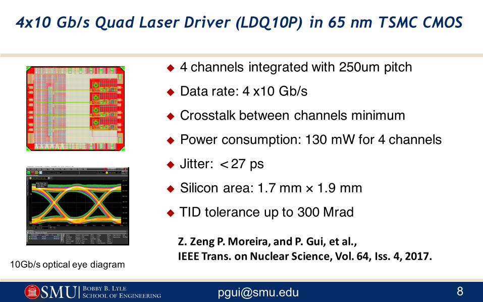
4x10 Gb/s Quad Laser Driver (LDQ10P) in 65 nm TSMC CMOS
u 4 channels integrated with 250um pitch
u Data rate: 4 x10 Gb/s
u Crosstalk between channels minimum
u Power consumption: 130 mW for 4 channels
u Jitter: < 27 ps
u Silicon area: 1.7 mm × 1.9 mm
u TID tolerance up to 300 Mrad
Z.ZengP.Moreira,andP.Gui,etal.,IEEETrans.onNuclearScience,Vol.64,Iss.4,2017.
10Gb/s optical eye diagram
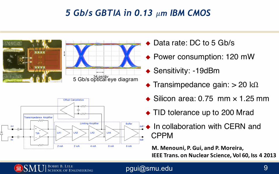
5 Gb/s GBTIA in 0.13 𝜇m IBM CMOS
u Data rate: DC to 5 Gb/s
u Power consumption: 120 mW
u Sensitivity: -19dBm
u Transimpedance gain: > 20 kΩ
u Silicon area: 0.75 mm × 1.25 mm
u TID tolerance up to 200 Mrad
u In collaboration with CERN and CPPMM.Menouni,P.Gui,andP.Moreira,IEEETrans.onNuclearScience,Vol60,Iss 42013
5 Gb/s optical eye diagram
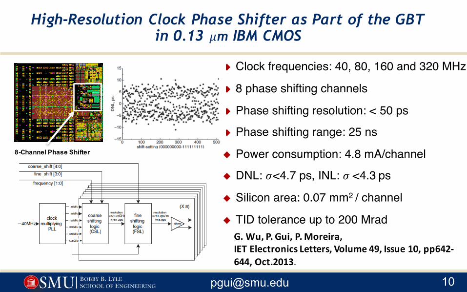
High-Resolution Clock Phase Shifter as Part of the GBT in 0.13 𝜇m IBM CMOS
u Clock frequencies: 40, 80, 160 and 320 MHz
u 8 phase shifting channels
u Phase shifting resolution: < 50 ps
u Phase shifting range: 25 ns
u Power consumption: 4.8 mA/channel
u DNL: 𝜎<4.7 ps, INL: 𝜎<4.3 ps
u Silicon area: 0.07 mm2 / channel
u TID tolerance up to 200 MradG.Wu,P.Gui,P.Moreira,IETElectronicsLetters,Volume49,Issue10,pp642-644,Oct.2013.
8-Channel Phase Shifter
IC Designs in Collaborations with Fermilab
u Cold PLL, serializer and line driver as part of COLDATA chip for protoDune
u PLL designed and demonstrated in room and cryogenic in 2015-2016
u Serializer as part of COLDATA chip in 65nm submitted in May 2017
u Transistor characterizations under room and cryogenic (77K)
u Both 0.13𝜇m and 65nm technologiesu Thermal analysis for the proto-VIPRAM00 chip
u URA (University Research Association) visiting scholars with Fermilab
u One MS thesis and 4 joint journal publications (IEEE TCAS-I 2017, IEEE TNS 2015, JINST 2015, and IEEE TDMR 2014)
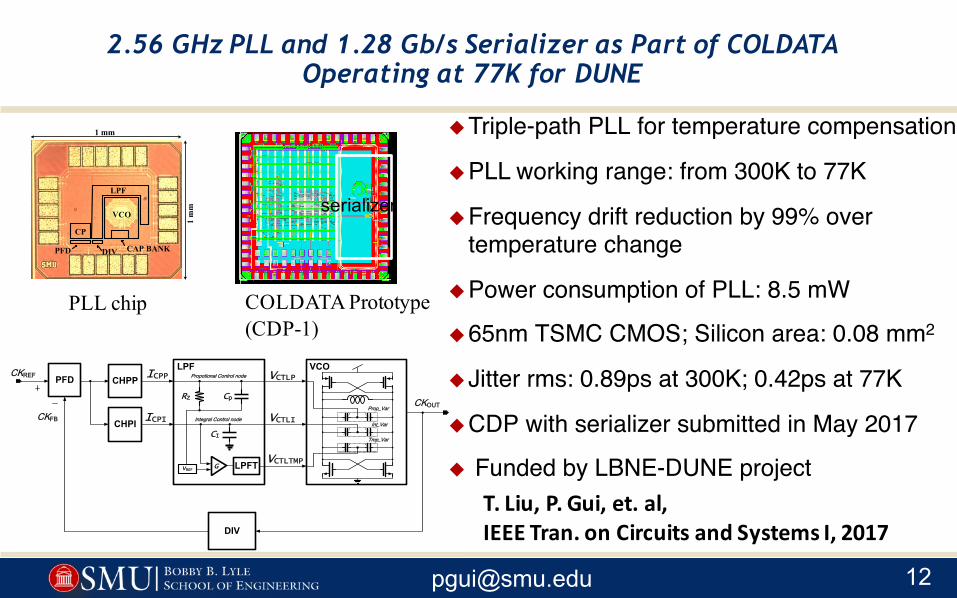
2.56 GHz PLL and 1.28 Gb/s Serializer as Part of COLDATA Operating at 77K for DUNE
uTriple-path PLL for temperature compensation
uPLL working range: from 300K to 77K
uFrequency drift reduction by 99% over temperature change
uPower consumption of PLL: 8.5 mW
u65nm TSMC CMOS; Silicon area: 0.08 mm2
uJitter rms: 0.89ps at 300K; 0.42ps at 77K
uCDP with serializer submitted in May 2017
u Funded by LBNE-DUNE projectT.Liu,P.Gui,et.al,IEEETran.onCircuitsandSystemsI,2017
1 mm
1 m
mLPF
DIV
CP
VCO
PFD CAP BANK
CHPI
DIV
VCTLPCKREF
CKOUT
CKFB
VCTLTMP
VCTLI
PFD LPF
ICPP
ICPI
CHPP
CI
Cp
LPFTG
VCO
VREF
Prop_Var
RZ
Tmp_Var
Int_VarIntegral Control node
Propotional Control node
PLL chip COLDATA Prototype (CDP-1)
serializer
[email protected] [email protected]
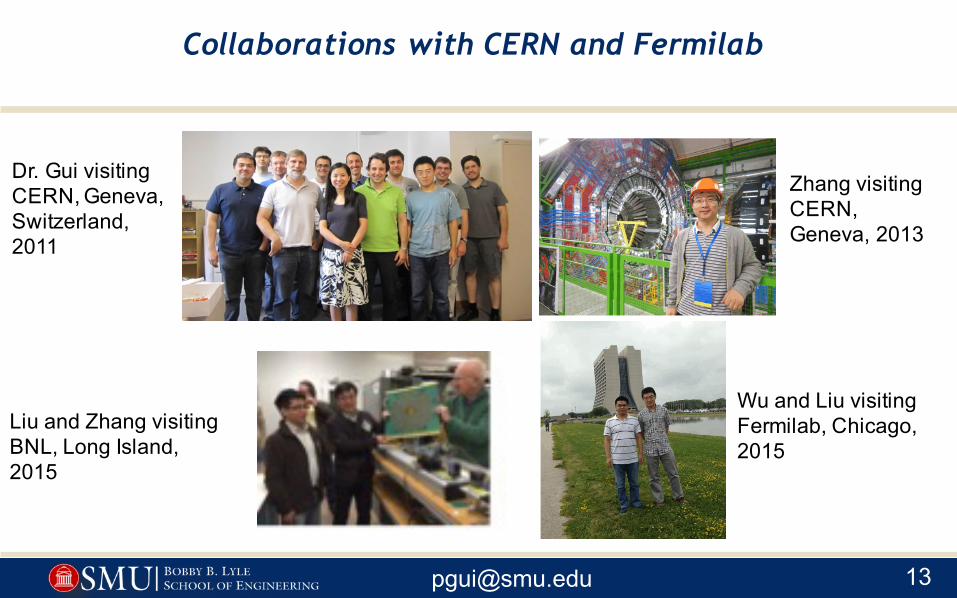
Dr. Gui visiting CERN, Geneva, Switzerland, 2011
Wu and Liu visiting Fermilab, Chicago, 2015
Liu and Zhang visiting BNL, Long Island, 2015
Zhang visiting CERN, Geneva, 2013
Collaborations with CERN and Fermilab
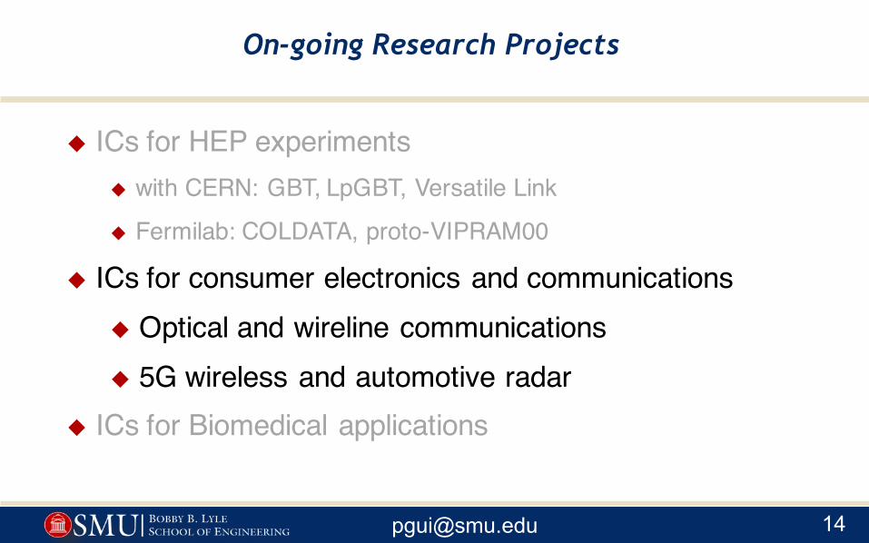
u ICs for HEP experiments u with CERN: GBT, LpGBT, Versatile Link
u Fermilab: COLDATA, proto-VIPRAM00
u ICs for consumer electronics and communicationsu Optical and wireline communicationsu 5G wireless and automotive radar
u ICs for Biomedical applications
On-going Research Projects
[email protected] [email protected]
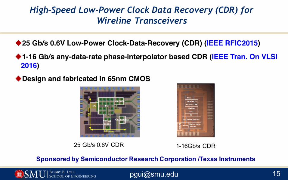
High-Speed Low-Power Clock Data Recovery (CDR) for Wireline Transceivers
u25 Gb/s 0.6V Low-Power Clock-Data-Recovery (CDR) (IEEE RFIC2015)
u1-16 Gb/s any-data-rate phase-interpolator based CDR (IEEE Tran. On VLSI 2016)
uDesign and fabricated in 65nm CMOS
25 Gb/s 0.6V CDR 1-16Gb/s CDR
Sponsored by Semiconductor Research Corporation /Texas Instruments
[email protected] [email protected]
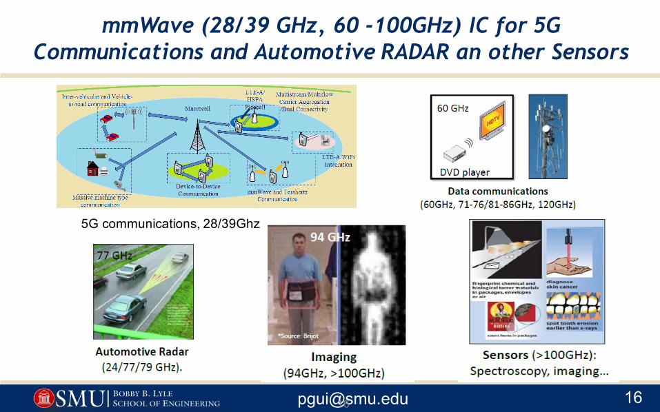
mmWave (28/39 GHz, 60 -100GHz) IC for 5G Communications and Automotive RADAR an other Sensors
16
5G communications, 28/39Ghz
[email protected] [email protected]
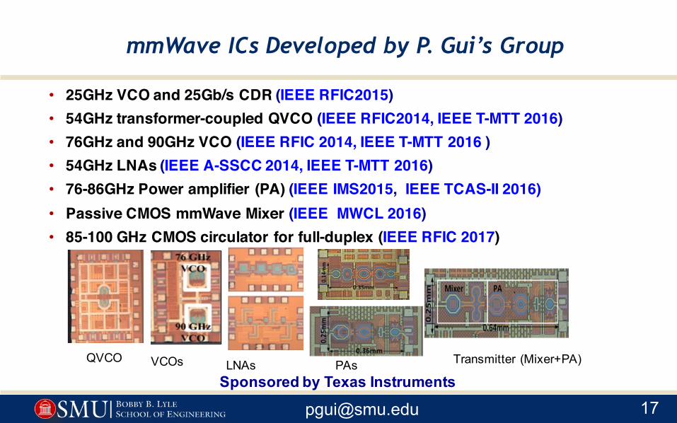
mmWave ICs Developed by P. Gui’s Group
• 25GHz VCO and 25Gb/s CDR (IEEE RFIC2015) • 54GHz transformer-coupled QVCO (IEEE RFIC2014, IEEE T-MTT 2016)• 76GHz and 90GHz VCO (IEEE RFIC 2014, IEEE T-MTT 2016 )• 54GHz LNAs (IEEE A-SSCC 2014, IEEE T-MTT 2016)• 76-86GHz Power amplifier (PA) (IEEE IMS2015, IEEE TCAS-II 2016)• Passive CMOS mmWave Mixer (IEEE MWCL 2016)• 85-100 GHz CMOS circulator for full-duplex (IEEE RFIC 2017)
QVCO VCOs LNAs PAs Transmitter (Mixer+PA)
Sponsored by Texas Instruments
[email protected] [email protected]
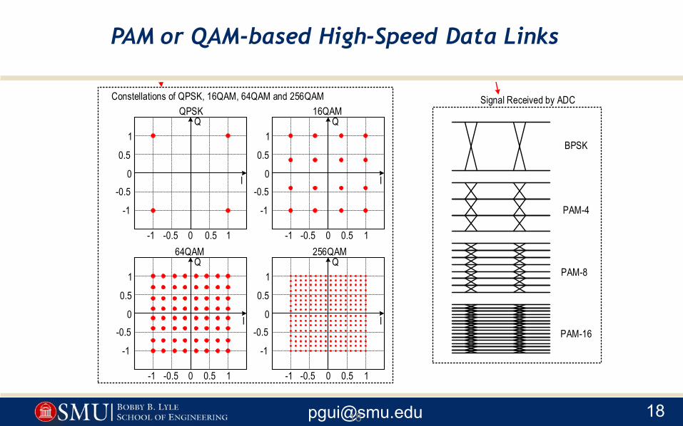
PAM or QAM-based High-Speed Data Links
18
90 DegreeMixer
90 DegreeMixer
XI
XQ
TIA
TIA
XIVPXIVNXQVPXQVN
YI
YQ
TIA
TIA
YIVPYIVNYQVPYQVN
ADC
ADC
ADC
ADC
DSPBeam Splitter
Polarizition Beam Splitter
LO Laser
Demodulator
Modulated SignalDP(Dual Plorization)-QPSK
DP-16QAMDP-64QAM
DP-256QAM
Coherent Receiver
Signal Received by ADC
I
Q
10.50-0.5-1
1
0.5
0-0.5
-1
QPSK
I
Q
10.50-0.5-1
1
0.5
0-0.5
-1
16QAM
I
Q
10.50-0.5-1
1
0.5
0-0.5
-1
64QAM
I
Q
10.50-0.5-1
1
0.5
0-0.5
-1
256QAM
Constellations of QPSK, 16QAM, 64QAM and 256QAM
BPSK
PAM-4
PAM-8
PAM-16
Fiber
[email protected] [email protected]
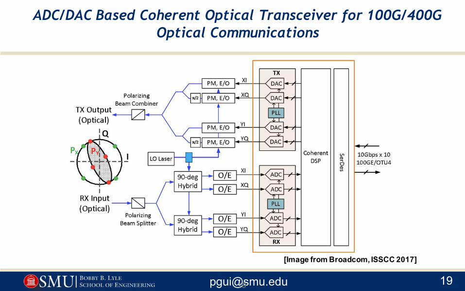
ADC/DAC Based Coherent Optical Transceiver for 100G/400G Optical Communications
19
[Image from Broadcom, ISSCC 2017]
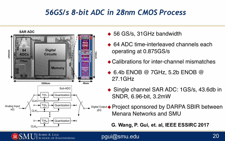
56GS/s 8-bit ADC in 28nm CMOS Process
G. Wang, P. Gui, et. al, IEEE ESSIRC 2017
T/H1
T/H2
T/HM Quantization
CLK1
Quantization
Quantization
CLK2
CLKM
Analog Inputx(t)
Digital Outputy[n]
Sub-ADC
u 56 GS/s, 31GHz bandwidth
u 64 ADC time-interleaved channels each operating at 0.875GS/s
uCalibrations for inter-channel mismatches
u 6.4b ENOB @ 7GHz, 5.2b ENOB @ 27.1GHz
u Single channel SAR ADC: 1GS/s, 43.6db in SNDR, 6.96-bit, 3.2mW
uProject sponsored by DARPA SBIR between Menara Networks and SMU
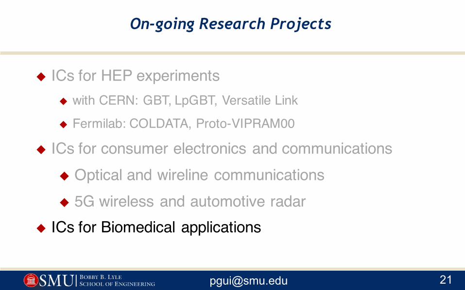
u ICs for HEP experiments u with CERN: GBT, LpGBT, Versatile Link
u Fermilab: COLDATA, Proto-VIPRAM00
u ICs for consumer electronics and communicationsu Optical and wireline communicationsu 5G wireless and automotive radar
u ICs for Biomedical applications
On-going Research Projects
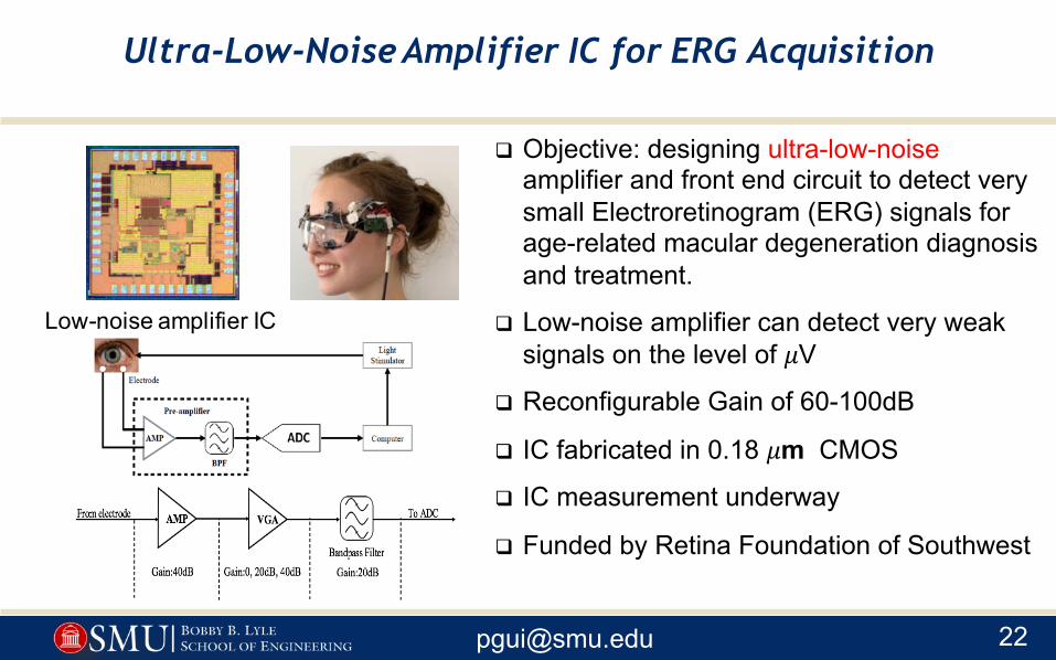
Ultra-Low-Noise Amplifier IC for ERG Acquisition
q Objective: designing ultra-low-noise amplifier and front end circuit to detect very small Electroretinogram (ERG) signals for age-related macular degeneration diagnosis and treatment.
q Low-noise amplifier can detect very weak signals on the level of 𝜇V
q Reconfigurable Gain of 60-100dB
q IC fabricated in 0.18 𝜇m CMOS
q IC measurement underway
q Funded by Retina Foundation of Southwest
Low-noise amplifier IC
Summary
u We work on analog/mixed-signal IC design with HEP community as well as with semiconductor industry and other foundations
u Extensive design experiences have been gained on high-speed and low-power design and on using advanced technologies from 180nm down to 28nm CMOS
u Continuing the efforts and collaborations