Embed Size (px)
Citation preview
Dharmapuri – 636 703
Regulation : 2013
Branch : B.E. – ECE
Year & Semester : II Year / IV Semester
ICAL ENG
EC6411 - CIRCUITS AND SIMULATIONINTEGRATED LABORATORY
LAB MANUAL
EC6411 CIRCUITS AND SIMULATION INTEGRATED LABORATORY 2
VVIT Department of Electronics and Communication Engineering
ANNA UNIVERSITY CHENNAIRegulation 2013
EC6411 CIRCUITS AND SIMULATION INTEGRATED LABORATORY
DESIGN AND ANALYSIS OF THE FOLLOWING CIRCUITS
1. Series and Shunt feedback amplifiers-Frequency response, Input and output impedance
calculation
2. RC Phase shift oscillator and Wien Bridge Oscillator
3. Hartley Oscillator and Colpits Oscillator
4. Single Tuned Amplifier
5. RC Integrator and Differentiator circuits
6. Astable and Monostable Multivibrators
7. Clippers and Clampers
8. Free running Blocking Oscillators
SIMULATION USING SPICE (Using Transistor):
9. Tuned Collector Oscillator
10. Twin -T Oscillator / Wein Bridge Oscillator
11. Double and Stager tuned Amplifiers
12. Bistable Multivibrator
13. Schmitt Trigger circuit with Predictable hysteresis
14. Monostable multivibrator with emitter timing and base timing
15. Voltage and Current Time base circuits
TOTAL: 45 Periods
EC6411 CIRCUITS AND SIMULATION INTEGRATED LABORATORY 3
VVIT Department of Electronics and Communication Engineering
INDEXEXPNo LIST OF EXPERIMENTS
PAGENo
SIGNATURE REMARKS
DESIGN AND ANALYSIS OF THE FOLLOWING CIRCUITS
1 Voltage Shunt Feedback Amplifier 15
2 Current Series Feedback Amplifier 21
3 RC Phase Shift Oscillator 29
4 Wein- Bridge Oscillator 35
5 Hartley Oscillator 39
6 Colpitt’s Oscillator 43
7 Single Tuned Amplifier 47
8 Integrator And Differentiator 53
9 Astable Multivibrator 57
10 Monostable Multivibrator 61
11 Clipper and Clamper Circuits 65
12 Free Running Blocking Oscillators 73
SIMULATION USING SPICE (Using Transistor):
13 Tuned Collector Oscillators 79
14 Twin-T Oscillator 81
15 Double and Stager Tuned Amplifiers 83
16 Bi-Stable Multivibrator 85
17Schmitt Trigger Circuit with PredictableHysteresis 87
18 Mono Stable Multivibrator 91
19 Voltage and Current Time Base Circuits 93
EC6411 CIRCUITS AND SIMULATION INTEGRATED LABORATORY 4
VVIT Department of Electronics and Communication Engineering
INTRODUCTION ABOUT CIRCUITS AND SIMULATION LAB
CIRCUITS LAB:
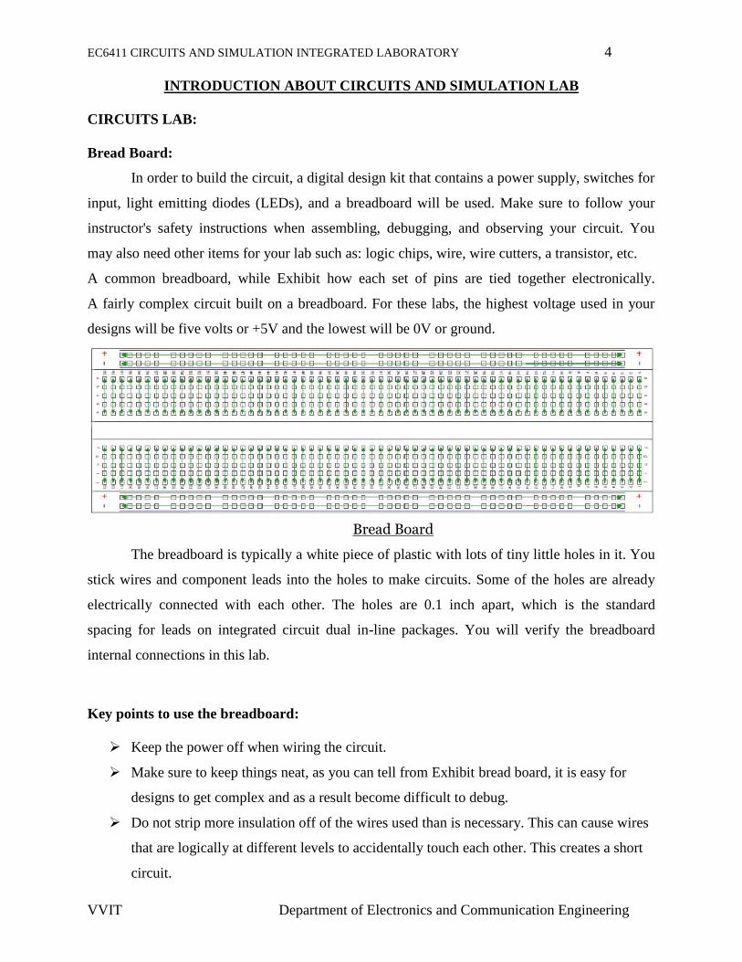
Bread Board:
In order to build the circuit, a digital design kit that contains a power supply, switches for
input, light emitting diodes (LEDs), and a breadboard will be used. Make sure to follow your
instructor's safety instructions when assembling, debugging, and observing your circuit. You
may also need other items for your lab such as: logic chips, wire, wire cutters, a transistor, etc.
A common breadboard, while Exhibit how each set of pins are tied together electronically.
A fairly complex circuit built on a breadboard. For these labs, the highest voltage used in your
designs will be five volts or +5V and the lowest will be 0V or ground.
Bread Board
The breadboard is typically a white piece of plastic with lots of tiny little holes in it. You
stick wires and component leads into the holes to make circuits. Some of the holes are already
electrically connected with each other. The holes are 0.1 inch apart, which is the standard
spacing for leads on integrated circuit dual in-line packages. You will verify the breadboard
internal connections in this lab.
Key points to use the breadboard:
Keep the power off when wiring the circuit.
Make sure to keep things neat, as you can tell from Exhibit bread board, it is easy for
designs to get complex and as a result become difficult to debug.
Do not strip more insulation off of the wires used than is necessary. This can cause wires
that are logically at different levels to accidentally touch each other. This creates a short
circuit.
EC6411 CIRCUITS AND SIMULATION INTEGRATED LABORATORY 5
VVIT Department of Electronics and Communication Engineering
Do not push the wires too far into each hole in the breadboard as this can cause two
different problems.
The wire can be pushed so far that only the insulation of the wire comes into contact with
the breadboard, causing an open circuit.
Too much wire is pushed into the hole; it curls under and ends up touching another
component at a different logical level. This causes a short circuit.
Use the longer outer rows for +5V on one side and ground on the other side.
Wire power to the circuit first using a common color (say red) for +5V and another
(black) for ground.
CIRCUIT SIMULATION
A common tool (computer aided design or CAD / electronic design automation or EDA
software) for the electronic circuit designer is circuit simulation software. Although most often
called simply a simulator, it is a software application that typically may include many functions
beyond electrical circuit simulation, including schematic capture, printed circuit board layout,
and bill of materials generation.
Most circuit simulator software grew out of a public domain program called SPICE
(Simulation Program with Integrated Circuit Emphasis) developed at UC Berkeley in the 1970s.
The original SPICE program operated in a batch mode and was text based. That is, the user
created a text file which described the circuit using special circuit netlist syntax. This file also
included simulation directives which told the software what type of simulation is to be
performed. The SPICE program read the input file, performed the appropriate analyses, and
produced a text output file that contained the results.

EC6411 CIRCUITS AND SIMULATION INTEGRATED LABORATORY 6
VVIT Department of Electronics and Communication Engineering
Over time EDA companies began adding graphical “back-ends” that could produce better
looking graphs and plots of the simulation results. A next obvious step was to add a graphical
interface for building the circuit (GUI). This had the dual benefit of both describing the circuit
for the simulation engine (generating the SPICE netlist) and allowing for the production of
publication quality schematic diagrams. Some of the early popular graphical versions included
PSpice and Electronics Workbench (EW being the precursor to Multisim).
More recent features include instrumentation simulation. That is, simulations of real
world commercial measurement devices may be used as part of the circuit simulation. In this
way, a sort of “virtual lab bench” may be created. With this feature, the circuit being designed
will look very similar to the actual circuit sitting on your lab bench. That is, if a transistor is used
in the simulation, it will look like a real transistor instead of the standard schematic symbol.
While this may initially appear to be very useful, especially for beginners, in practical terms it
sometimes slows down the design process by making the schematic less clear and more cluttered
to the user.
PSPICE SOFTWARE PROCEDURE.
1. Run the CAPTURE (SPICE) program.
2. Select File/New/Project from the File menu.
3. On the New Project window select Analog or Mixed A/D, and give a name to your project
then click OK.
4. The Create PSpice Project window will pop up, select Create a blank project, and then click
OK.
5. Now you will be in the schematic environment where you are to build your circuit.
6. Select Place/Part from the Place menu.
7. Click ANALOG from the box called Libraries: then look for the part called R. You can do it
either by scrolling down on the Part List: box or by typing R on the Part box. Then click OK.
8. Use the mouse to place the resistor where you want and then click to leave the resistor there.
You can continue placing as many resistors as you need and once you have finished placing
the resistors right-click your mouse and select end mode.
EC6411 CIRCUITS AND SIMULATION INTEGRATED LABORATORY 7
VVIT Department of Electronics and Communication Engineering
9. To rotate the components there are two options:
Rotate a component once it is placed: Select the component by clicking on it then Ctrl-R
Rotate the component before it is placed: Just Ctrl-R.
10. Select Place/Part from the Place menu.
11. Click SOURCE from the box called Libraries:, then look for the part called VDC. You can
do it either by scrolling down on the Part List: box or by typing VDC on the Part box, and then
click OK. Place the Source.
12. Repeat steps 10 - 12 to get and place a current source named IDC.
13. Select Place/Wire and start wiring the circuit. To start a wire click on the component terminal
where you want it to begin, and then click on the component terminal where you want it to
finish. You can continue placing wires until all components are wired. Then right-click and
select end wire.
14. Select Place/Ground from the Place menu, click on GND/CAPSYM. Now you will see the
ground symbol. Type 0 on the Name: box and then click OK. Then place the ground. Wire it
if necessary.
16. Now change the component values to the required ones. To do this you just need to double-
click on the parameter you want to change. A window will pop up where you will be able to
set a new value for that parameter.
17. Once you have finished building your circuit, you can move on to the next step – prepare it
for simulation.
18. Select PSpice/New Simulation Profile and type a name, this can be the same name as your
project, and click Create.
19. The Simulations Settings window will now appear. You can set up the type of analysis you
want PSpice to perform. In this case it will be Bias Point. Click Apply then OK.
20. Now you are ready to simulate the circuit. Select PSpice/Run and wait until the PSpice
finishes. Go back to Capture and see the voltages and currents on all the nodes.
21. If you are not seeing any readout of the voltages and currents then select PSpice/Bias
Point/Enable Bias Voltage Display and PSpice/Bias Point/Enable Bias Current Display. Make
sure that PSpice/ Bias Point/Enable is checked.
EC6411 CIRCUITS AND SIMULATION INTEGRATED LABORATORY 8
VVIT Department of Electronics and Communication Engineering
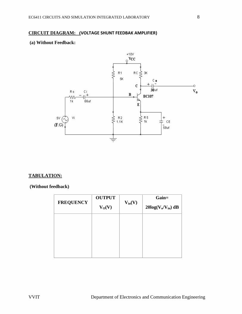
CIRCUIT DIAGRAM: (VOLTAGE SHUNT FEEDBAK AMPLIFIER)
(a) Without Feedback:
TABULATION:
(Without feedback)
FREQUENCYOUTPUT
VO(V)Vin(V)
Gain=
20log(Vo/Vin) dB
EC6411 CIRCUITS AND SIMULATION INTEGRATED LABORATORY 8
VVIT Department of Electronics and Communication Engineering
CIRCUIT DIAGRAM: (VOLTAGE SHUNT FEEDBAK AMPLIFIER)
(a) Without Feedback:
TABULATION:
(Without feedback)
FREQUENCYOUTPUT
VO(V)Vin(V)
Gain=
20log(Vo/Vin) dB
EC6411 CIRCUITS AND SIMULATION INTEGRATED LABORATORY 8
VVIT Department of Electronics and Communication Engineering
CIRCUIT DIAGRAM: (VOLTAGE SHUNT FEEDBAK AMPLIFIER)
(a) Without Feedback:
TABULATION:
(Without feedback)
FREQUENCYOUTPUT
VO(V)Vin(V)
Gain=
20log(Vo/Vin) dB
EC6411 CIRCUITS AND SIMULATION INTEGRATED LABORATORY 9
VVIT Department of Electronics and Communication Engineering
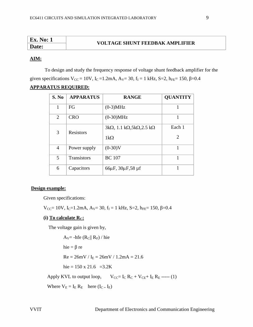
Ex. No: 1VOLTAGE SHUNT FEEDBAK AMPLIFIER
Date:
AIM:
To design and study the frequency response of voltage shunt feedback amplifier for the
given specifications VCC = 10V, IC =1.2mA, AV= 30, fI = 1 kHz, S=2, hFE= 150, β=0.4
APPARATUS REQUIRED:
S. No APPARATUS RANGE QUANTITY
1 FG (0-3)MHz 1
2 CRO (0-30)MHz 1
3 Resistors3k, 1.1 k,5k,2.5 k
1k
Each 1
2
4 Power supply (0-30)V 1
5 Transistors BC 107 1
6 Capacitors 66F, 30F,58 µf 1
Design example:
Given specifications:
VCC= 10V, IC=1.2mA, AV= 30, fI = 1 kHz, S=2, hFE= 150, β=0.4
(i) To calculate RC:
The voltage gain is given by,
AV= -hfe (RC|| RF) / hie
hie = β re
Re = 26mV / IE = 26mV / 1.2mA = 21.6
hie = 150 x 21.6 =3.2K
Apply KVL to output loop, VCC= IC RC + VCE+ IE RE ----- (1)
Where VE = IE RE here (IC ~ IE)
EC6411 CIRCUITS AND SIMULATION INTEGRATED LABORATORY 10
VVIT Department of Electronics and Communication Engineering
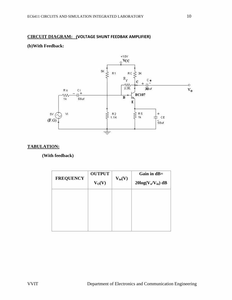
CIRCUIT DIAGRAM: (VOLTAGE SHUNT FEEDBAK AMPLIFIER)
(b)With Feedback:
TABULATION:
(With feedback)
FREQUENCYOUTPUT
VO(V)Vin(V)
Gain in dB=
20log(Vo/Vin) dB
EC6411 CIRCUITS AND SIMULATION INTEGRATED LABORATORY 10
VVIT Department of Electronics and Communication Engineering
CIRCUIT DIAGRAM: (VOLTAGE SHUNT FEEDBAK AMPLIFIER)
(b)With Feedback:
TABULATION:
(With feedback)
FREQUENCYOUTPUT
VO(V)Vin(V)
Gain in dB=
20log(Vo/Vin) dB
EC6411 CIRCUITS AND SIMULATION INTEGRATED LABORATORY 10
VVIT Department of Electronics and Communication Engineering
CIRCUIT DIAGRAM: (VOLTAGE SHUNT FEEDBAK AMPLIFIER)
(b)With Feedback:
TABULATION:
(With feedback)
FREQUENCYOUTPUT
VO(V)Vin(V)
Gain in dB=
20log(Vo/Vin) dB
EC6411 CIRCUITS AND SIMULATION INTEGRATED LABORATORY 11
VVIT Department of Electronics and Communication Engineering
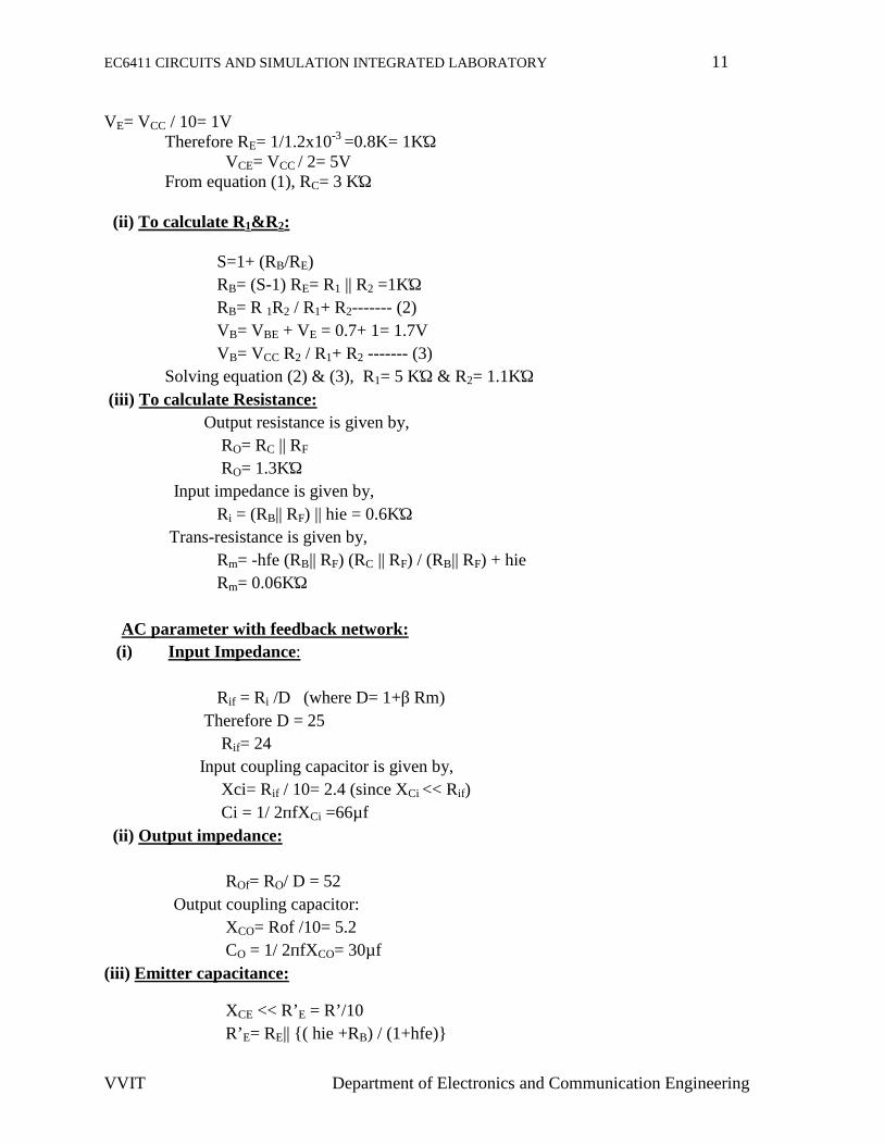
VE= VCC / 10= 1VTherefore RE= 1/1.2x10-3 =0.8K= 1KΏ
VCE= VCC / 2= 5VFrom equation (1), RC= 3 KΏ
(ii) To calculate R1&R2:
S=1+ (RB/RE)RB= (S-1) RE= R1 || R2 =1KΏRB= R 1R2 / R1+ R2------- (2)VB= VBE + VE = 0.7+ 1= 1.7VVB= VCC R2 / R1+ R2 ------- (3)
Solving equation (2) & (3), R1= 5 KΏ & R2= 1.1KΏ(iii) To calculate Resistance:
Output resistance is given by,RO= RC || RF
RO= 1.3KΏInput impedance is given by,
Ri = (RB|| RF) || hie = 0.6KΏTrans-resistance is given by,
Rm= -hfe (RB|| RF) (RC || RF) / (RB|| RF) + hieRm= 0.06KΏ
AC parameter with feedback network:(i) Input Impedance:
Rif = Ri /D (where D= 1+β Rm)Therefore D = 25
Rif= 24Input coupling capacitor is given by,
Xci= Rif / 10= 2.4 (since XCi << Rif)Ci = 1/ 2пfXCi =66µf
(ii) Output impedance:
ROf= RO/ D = 52Output coupling capacitor:
XCO= Rof /10= 5.2CO = 1/ 2пfXCO= 30µf
(iii) Emitter capacitance:
XCE << R’E = R’/10R’E= RE|| ( hie +RB) / (1+hfe)
EC6411 CIRCUITS AND SIMULATION INTEGRATED LABORATORY 12
VVIT Department of Electronics and Communication Engineering
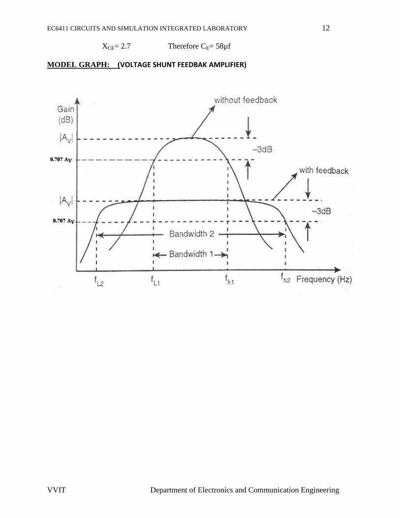
XCE= 2.7 Therefore CE= 58µf
MODEL GRAPH: (VOLTAGE SHUNT FEEDBAK AMPLIFIER)
EC6411 CIRCUITS AND SIMULATION INTEGRATED LABORATORY 13
VVIT Department of Electronics and Communication Engineering
THEORY:
Negative feedback in general increases the bandwidth of the transfer function
stabilized by the specific type of feedback used in a circuit. In Voltage shunt feedback
amplifier, consider a common emitter stage with a resistance R’ connected from collector to
base. This is a case of voltage shunt feedback and we expect the bandwidth of the Trans
resistance to be improved due to the feedback through R’. The voltage source is represented by
its Norton’s equivalent current source IS=Vs/Rs.
PROCEDURE:
1. Connect the amplifier without feedback circuit as per the circuit diagram.
2. Set VCC = 10V; set input voltage using audio frequency oscillator.
3. By varying audio frequency oscillator take down output frequency oscillator voltage
for difference in frequency.
4. Calculate the gain in dB.
5. Plot gain Vs frequency curve in semi-log sheet.
6. Connect the amplifier with feedback circuit as per the circuit diagram.
7. Set VCC = 10V; set input voltage using audio frequency oscillator.
8. By varying audio frequency oscillator take down output frequency oscillator voltage
for difference in frequency.
9. Calculate the gain in dB
10. Plot gain Vs frequency curve in semi-log sheet.
11. Compare response with respect to the amplifier with and without feedback.
Abbreviations:
FG – Function Generator.
CRO- Cathode Ray Oscilloscope.
VO – Output Voltage; Vi – Input Voltage.
dB – Decibel unit
RESULT:
Thus voltage shunt feedback amplifier is designed and Bandwidth is calculated.
EC6411 CIRCUITS AND SIMULATION INTEGRATED LABORATORY 14
VVIT Department of Electronics and Communication Engineering
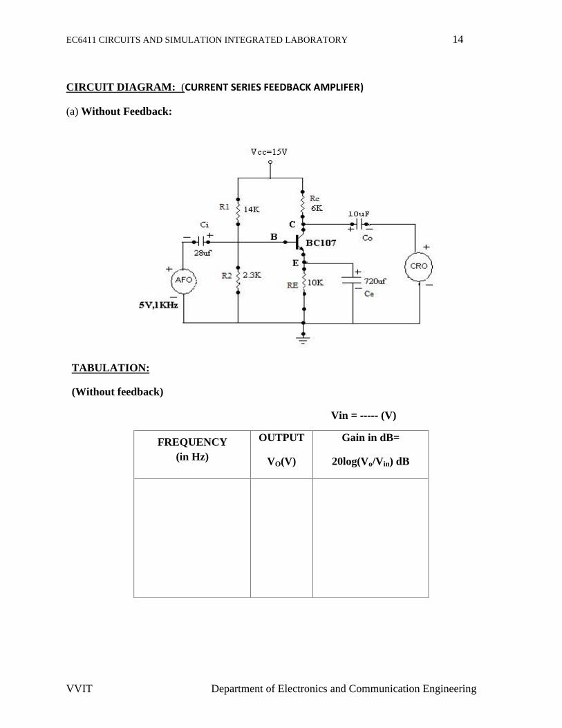
CIRCUIT DIAGRAM: (CURRENT SERIES FEEDBACK AMPLIFER)
(a) Without Feedback:
TABULATION:
(Without feedback)
Vin = ----- (V)
FREQUENCY(in Hz)
OUTPUT
VO(V)
Gain in dB=
20log(Vo/Vin) dB
EC6411 CIRCUITS AND SIMULATION INTEGRATED LABORATORY 15
VVIT Department of Electronics and Communication Engineering
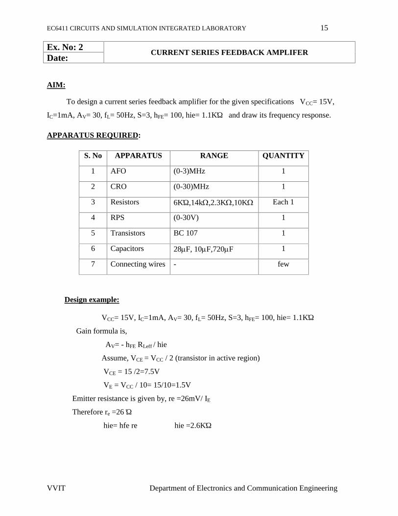
Ex. No: 2CURRENT SERIES FEEDBACK AMPLIFER
Date:
AIM:
To design a current series feedback amplifier for the given specifications VCC= 15V,
IC=1mA, AV= 30, fL= 50Hz, S=3, hFE= 100, hie= 1.1KΏ and draw its frequency response.
APPARATUS REQUIRED:
S. No APPARATUS RANGE QUANTITY
1 AFO (0-3)MHz 1
2 CRO (0-30)MHz 1
3 Resistors 6KΏ,14k,2.3K,10K Each 1
4 RPS (0-30V) 1
5 Transistors BC 107 1
6 Capacitors 28F, 10F,720F 1
7 Connecting wires - few
Design example:
VCC= 15V, IC=1mA, AV= 30, fL= 50Hz, S=3, hFE= 100, hie= 1.1KΏ
Gain formula is,
AV= - hFE RLeff / hie
Assume, VCE = VCC / 2 (transistor in active region)
VCE = 15 /2=7.5V
VE = VCC / 10= 15/10=1.5V
Emitter resistance is given by, re =26mV/ IE
Therefore re =26 Ώ
hie= hfe re hie =2.6KΏ
EC6411 CIRCUITS AND SIMULATION INTEGRATED LABORATORY 16
VVIT Department of Electronics and Communication Engineering
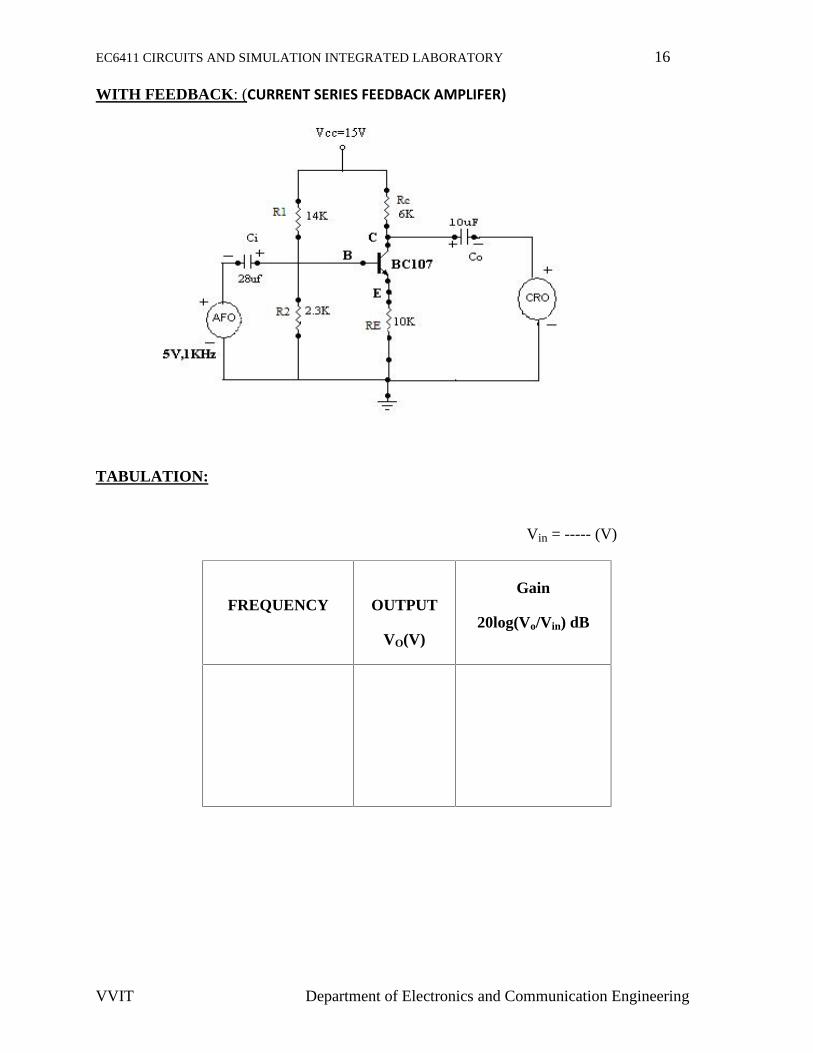
WITH FEEDBACK: (CURRENT SERIES FEEDBACK AMPLIFER)
TABULATION:
Vin = ----- (V)
FREQUENCY OUTPUT
VO(V)
Gain
20log(Vo/Vin) dB
EC6411 CIRCUITS AND SIMULATION INTEGRATED LABORATORY 17
VVIT Department of Electronics and Communication Engineering
(i) To calculate RC:
Applying KVL to output loop,
VCC= IC RC + VCE+ IE RE ----- (1)
Where RE = VE / IE (IC= IE)
RE = 1.5 / 1x10-3= 1.5KΏ
From equation (1),
RC= 6KΏ
(ii) To calculate RB1&RB2:
Since IB is small when compared with IC,
IC ~ IE
VB= VBE + VE= 0.7 + 1.5=2.2V
VB= VCC (RB2 / RB1+ RB2) ----- (2)
S=1+ (RB / RE)
RB= 2KΏ
We know that RB= RB1|| RB2
RB= R B1RB2/ RB1+RB2--------- (3)
Solving equation (2) & (3),
Therefore,
RB1 = 14KΏ
From equation (3), RB2= 2.3KΏ
(iii) To find input coupling capacitor (Ci):
XCi = (hie|| RB) / 10
XCi = 113
XCi= 1/ 2пf Ci
Ci = 1 / 2пf XCi
Ci = 1/ 2X3.14X 50 X 113=28µf
EC6411 CIRCUITS AND SIMULATION INTEGRATED LABORATORY 18
VVIT Department of Electronics and Communication Engineering
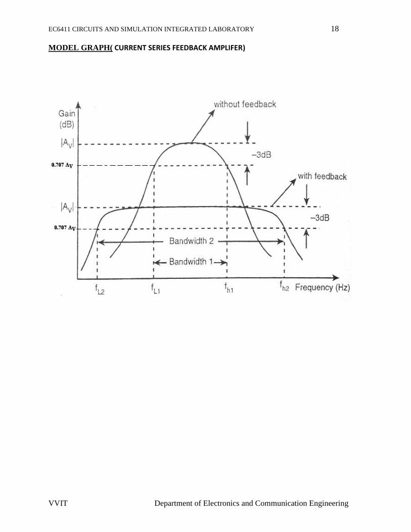
MODEL GRAPH( CURRENT SERIES FEEDBACK AMPLIFER)
EC6411 CIRCUITS AND SIMULATION INTEGRATED LABORATORY 19
VVIT Department of Electronics and Communication Engineering
(iv)To find output coupling capacitor (CO):
XCO= (RC || RL) / 10, (Assume RL= 10KΏ)
XCO= 375
XCO= 1/ 2пf CO
CO = 1/ 2x 3.14x 50 x 375=8µf =10 µf
(v) To find Bypass capacitor (CE):
(Without feedback)
XCE = (RB + hie / 1+ hfe) || RE/ 10
XCE = 4.416
CE= 1 / 2пf XCE
CE = 720 µf
Design with feedback:
To design with feedback remove the bypass capacitor (CE).
Assume RE = 10K
THEORY:
Negative feedback in general increases the bandwidth of the transfer function
stabilized by the specific type of feedback used in a circuit. In Voltage series feedback amplifier,
consider a common emitter stage with a resistance R’ connected from emitter to ground. This is
a case of voltage series feedback and we expect the bandwidth of the Trans resistance to be
improved due to the feedback through R’ .The voltage source is represented by its Norton’s
equivalent current source Is=Vs/Rs.
EC6411 CIRCUITS AND SIMULATION INTEGRATED LABORATORY 20
VVIT Department of Electronics and Communication Engineering
PROCEDURE:
1. Connect the circuit as per the circuit diagram.
2. Set VCC = 10V; set input voltage using audio frequency oscillator.
3. By varying audio frequency oscillator take down output
frequency oscillator voltage for difference in frequency.
4. Calculate the gain in dB
5. Plot gain Vs frequency curve in semi-log sheet.
Abbreviations:
AFO – Audio frequency oscillator.
CRO - Cathode Ray Oscilloscope.
VO – Output Voltage; Vi – Input Voltage.
dB – Decibel unit
RPS – Regulated Power Supply.
RESULT:
Thus current series feedback amplifier is designed and Bandwidth is calculated.
EC6411 CIRCUITS AND SIMULATION INTEGRATED LABORATORY 21
VVIT Department of Electronics and Communication Engineering
CIRCUIT DIAGRAM: (RC PHASE SHIFT OSCILLATOR)
MODEL GRAPH:
Amplitude (V)
Time (sec)
EC6411 CIRCUITS AND SIMULATION INTEGRATED LABORATORY 22
VVIT Department of Electronics and Communication Engineering
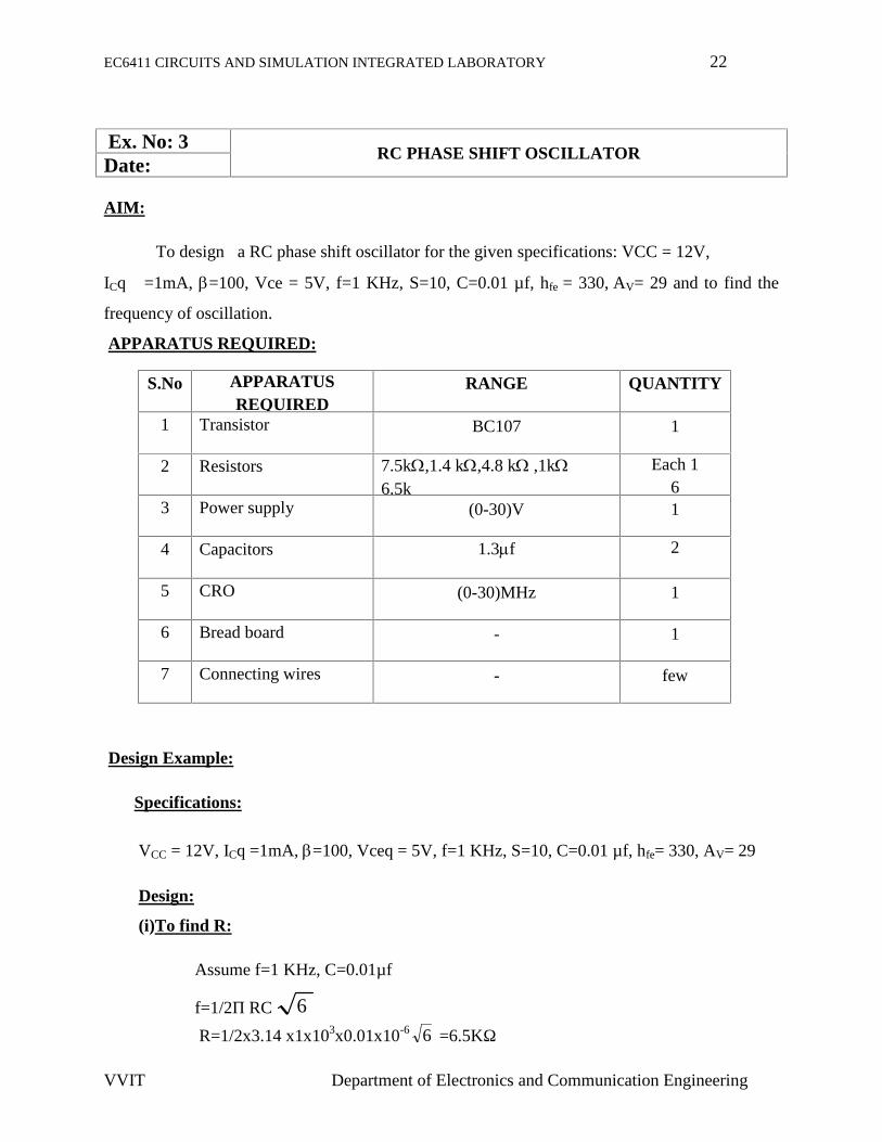
Ex. No: 3RC PHASE SHIFT OSCILLATOR
Date:
AIM:
To design a RC phase shift oscillator for the given specifications: VCC = 12V,
ICq =1mA, =100, Vce = 5V, f=1 KHz, S=10, C=0.01 µf, hfe = 330, AV= 29 and to find the
frequency of oscillation.
APPARATUS REQUIRED:
S.No APPARATUSREQUIRED
RANGE QUANTITY
1 Transistor BC107 1
2 Resistors 7.5k,1.4 k,4.8 k ,1k6.5k
6.5K
Each 16
3 Power supply (0-30)V 1
4 Capacitors 1.3f
0.01F
2
3
3
5 CRO (0-30)MHz 1
6 Bread board - 1
7 Connecting wires - few
Design Example:
Specifications:
VCC = 12V, ICq =1mA, =100, Vceq = 5V, f=1 KHz, S=10, C=0.01 µf, hfe= 330, AV= 29
Design:
(i)To find R:
Assume f=1 KHz, C=0.01µf
f=1/2П RC 6
R=1/2x3.14 x1x103x0.01x10-6 6 =6.5KΩ
EC6411 CIRCUITS AND SIMULATION INTEGRATED LABORATORY 23
VVIT Department of Electronics and Communication Engineering
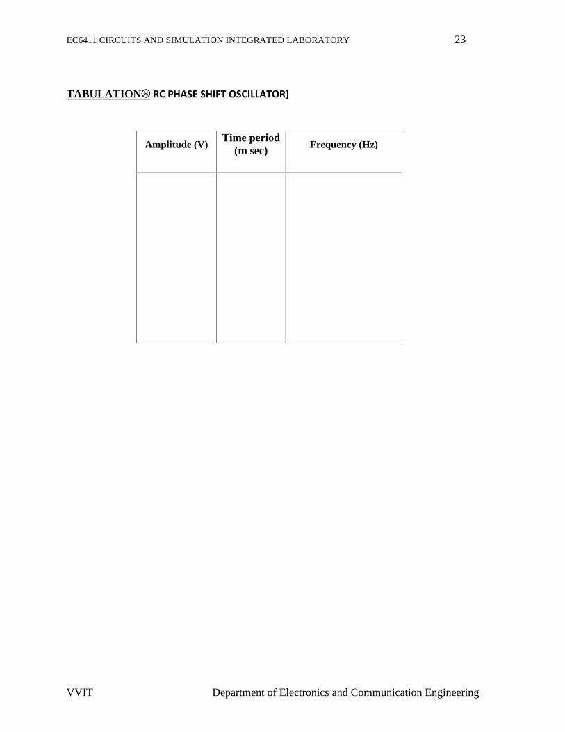
TABULATION RC PHASE SHIFT OSCILLATOR)
Amplitude (V)Time period
(m sec)Frequency (Hz)
EC6411 CIRCUITS AND SIMULATION INTEGRATED LABORATORY 24
VVIT Department of Electronics and Communication Engineering
(ii)To find RE & RC:
VCE = VCC /2 = 6V
re= 26mV / IE= 26
hie = hfe re= 330 x 26= 8580
On applying KVL to output loop,
VCC=ICRC + VCE + IERE ----- (1)
VE = IE RE
RE = VE / IE =1.2/ 10-3 =1.2K
From equation (1), 12= 10-3(RC+ 1200) +6= RC= 4800=4.8K
(iii)To calculate R1 & R2:
VBB= VCC R2 / R1+ R2 ------ (2)
VB= VBE +VE = 0.7+12 =1.9V
From equation (2), 1.9= 12 R2 / R1+ R2
R2 / R1+ R2= 0.158 -------- (3)
S = 1+ RB / RE= RB = 1.2K
RB =R1 || R2
0.15R1= 1.2x10-3=7.5K
R2 =0.158 R1 + 0.158 R2, R2= 1.425K
EC6411 CIRCUITS AND SIMULATION INTEGRATED LABORATORY 25
VVIT Department of Electronics and Communication Engineering
(iv)To calculate Coupling capacitors:
(i) XCi= [hie + (1+hfe) RE] || RB / 10 = 0.12K
XCi= 1 / 2∏ f Ci == 1.3f
(ii) XCO= RLeff / 10 [ AV = - hfe RLeff / hie]
RLeff = 0.74K, XCO=0.075 K
XCO= 1 / 2∏ f CO , CO = 2.1f
(iii) XCE= RE / 10 = 1.326 f; XCE = 1 / 2∏ f CE=49.
(iv) Feedback capacitor, XCF = Rf / 10 ;Cf = 0.636f = 0.01f
THEORY:
The low frequencies RC oscillators are more suitable. Tuned circuit is not an
essential requirement for oscillation. The essential requirement is that there must be a 180o
phase shift around the feedback network and loop gain should be greater than unity. The 180o
phase shift in feedback signal can be achieved by suitable RC network.
PROCEDURE:
1. Connect the circuit as per the circuit diagram.
2. Set VCC = 15V.
3. For the given supply the amplitude and time period is measured from CRO.
4. Frequency of oscillation is calculated by the formula f=1/T.
5. Amplitude Vs time graph is drawn.
Abbreviations:
Av – Voltage Gain.
Β – Stability Factor
f - Frequency
KVL – Kirchhoff Voltage Law
RESULT:
Thus the RC-phase shift oscillator is designed and constructed for the given
frequency.
Frequency :
EC6411 CIRCUITS AND SIMULATION INTEGRATED LABORATORY 26
VVIT Department of Electronics and Communication Engineering
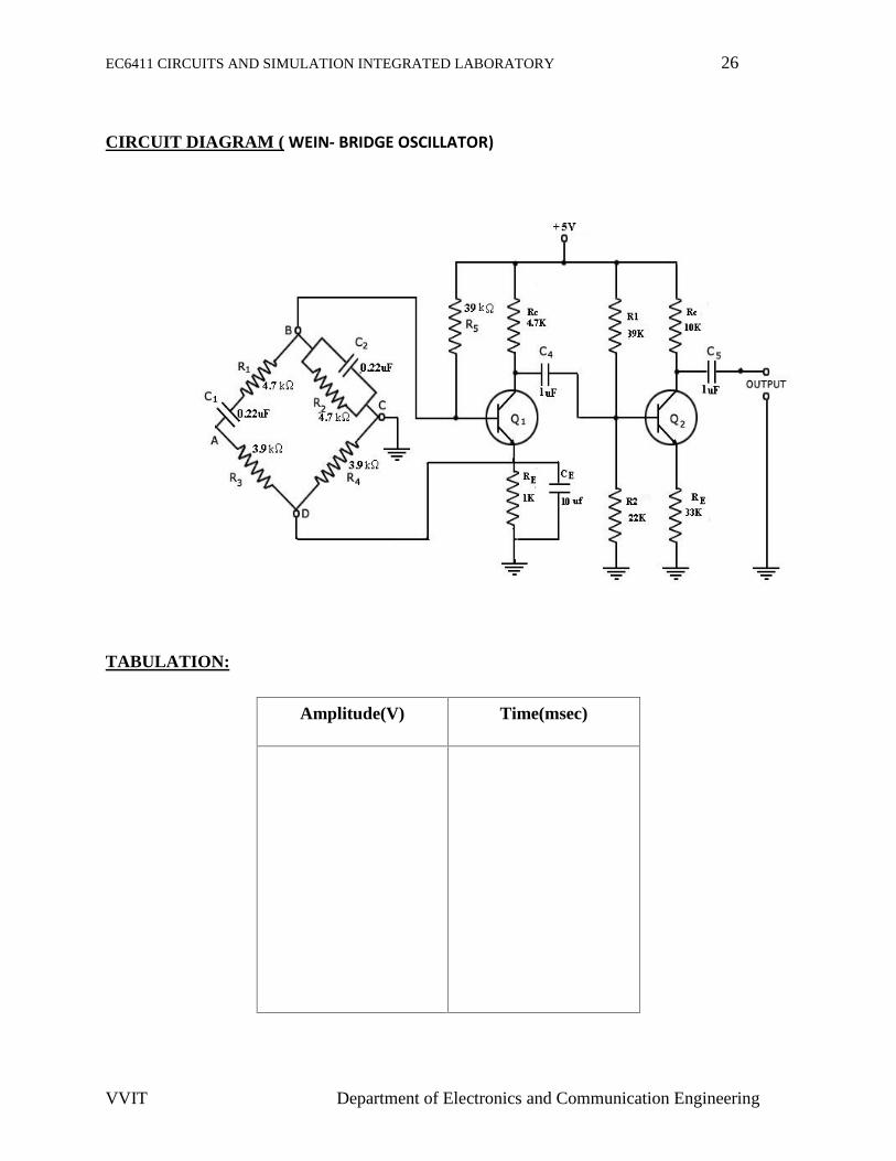
CIRCUIT DIAGRAM ( WEIN- BRIDGE OSCILLATOR)
TABULATION:
Amplitude(V) Time(msec)
EC6411 CIRCUITS AND SIMULATION INTEGRATED LABORATORY 27
VVIT Department of Electronics and Communication Engineering
Ex. No: 4WEIN- BRIDGE OSCILLATOR
Date:
AIM:
To design a Wein-bridge oscillator using transistors and to find the frequency of
oscillation for the given operating frequency 1 KHz.
APPARATUS REQUIRED:
S.No APPARATUSREQUIRED
RANGE QUANTITY
1 Resistors 3.9 k, 4.7 k, 39k,
1k, 10k,22K,33k2,3,2,1,1,1,1
2 Power supply (0-30)V 1
3 Transistor BC107 2
4 Capacitors 0.22F,1F
10F
Each 2
15 CRO (0-30)MHz 1
6 Bread board -
-
1
7 Connecting wires - few
THEORY:
Generally in an oscillator, amplifier stage introduces 180o phase shift and
feedback network introduces additional 180o phase shift, to obtain a phase shift of 360o around a
loop. This is a condition for any oscillator. But Wein bridge oscillator ses a non-inverting
amplifier and hence does not provide any phase shift during amplifier stage. As total phase shift
requires is 0o or 2n radians, in Wein bridge type no phase shift is necessary through feedback.
Thus the total phase shift around a loop is 0o.
EC6411 CIRCUITS AND SIMULATION INTEGRATED LABORATORY 28
VVIT Department of Electronics and Communication Engineering
The output of the amplifier is applied between the terminals 1 and 3, which are
the input to the feedback network. While the amplifier input is supplied from the diagonal
terminals 2 and 4, which is the output from the feedback network. Thus amplifier supplied its
own output through the Wein Bridge as a feedback network.
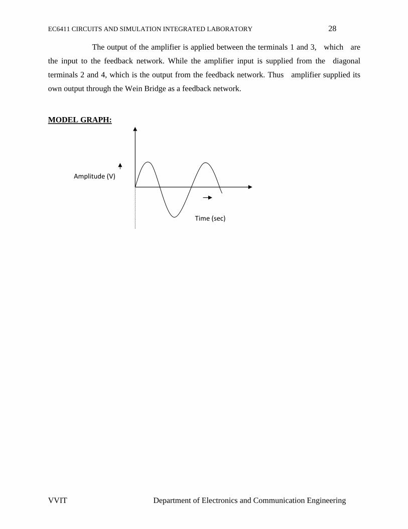
MODEL GRAPH:
Amplitude (V)
Time (sec)
EC6411 CIRCUITS AND SIMULATION INTEGRATED LABORATORY 29
VVIT Department of Electronics and Communication Engineering
The two arms of the bridge, namely R1, C1 in series and R2, C2 in parallel are called
frequency sensitive arms. This is because the components of these two arms decide the
frequency of the oscillator.
PROCEDURE:
1. Connect the circuit as per the circuit diagram.
2. Set VCC = 5V.
3. For the given supply the amplitude and time period is measured from CRO.
4. Frequency of oscillation is calculated by the formula f=1/T
5. Amplitude Vs Time graph is drawn.
RESULT:
Thus the Wein – bridge oscillator is designed for the given frequency of oscillation.
Frequency :
EC6411 CIRCUITS AND SIMULATION INTEGRATED LABORATORY 30
VVIT Department of Electronics and Communication Engineering
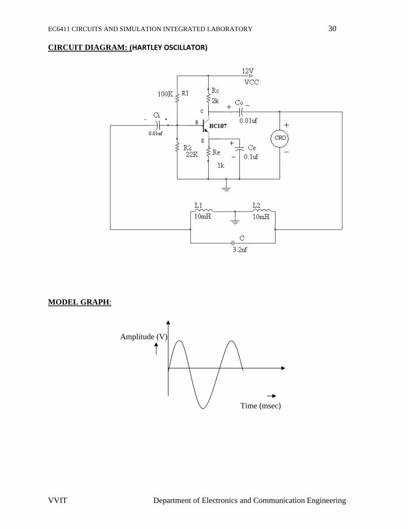
CIRCUIT DIAGRAM: (HARTLEY OSCILLATOR)
MODEL GRAPH:
Amplitude (V)
Time (msec)
EC6411 CIRCUITS AND SIMULATION INTEGRATED LABORATORY 30
VVIT Department of Electronics and Communication Engineering
CIRCUIT DIAGRAM: (HARTLEY OSCILLATOR)
MODEL GRAPH:
Amplitude (V)
Time (msec)
EC6411 CIRCUITS AND SIMULATION INTEGRATED LABORATORY 30
VVIT Department of Electronics and Communication Engineering
CIRCUIT DIAGRAM: (HARTLEY OSCILLATOR)
MODEL GRAPH:
Amplitude (V)
Time (msec)
EC6411 CIRCUITS AND SIMULATION INTEGRATED LABORATORY 31
VVIT Department of Electronics and Communication Engineering
Ex.No.5HARTLEY OSCILLATOR
Date:
AIM:
To design and construct a Hartley oscillator for the given specifications L1= L2=10mH,
f=20 KHz, VCC=12V, IC=3mA, S=12
APPARATUS REQUIRED:
S.No APPARATUSREQUIRED
RANGE QUANTITY
1 Resistors 2k,1K,100 k,22k Each one
2 RPS (0-30)V 1
3 Transistor BC107 1
4 Capacitors 3.2nf,0.1F, 0.01F
0.01F
Each 1
25 Inductor 10mH 2
6 CRO (0-30)MHz 1
7 Bread board - 1
8 Connecting wires - few
Design Example:
Design of feedback Network:
Given L1= L2=10mH, f=20 KHz, VCC=12V, IC=3mA, S=12
Frequency Formula:
F=1/2П LeqC , Where, Leq = L1+L2
Therefore,
F = 1/2П CLL )21(
C= 3.2nf
EC6411 CIRCUITS AND SIMULATION INTEGRATED LABORATORY 32
VVIT Department of Electronics and Communication Engineering
TABULATION( HARTLEY OSCILLATOR)
Amplitude(V) Time(msec) Frequency(Hz)
EC6411 CIRCUITS AND SIMULATION INTEGRATED LABORATORY 33
VVIT Department of Electronics and Communication Engineering
THEORY:
Hartley oscillator is very popular and is commonly used as local oscillator in radio
receivers. The collector voltage is applied to the collector through inductor L whose reactance is
high compared with X2 and may therefore be omitted from equivalent circuit, at zero frequency,
however capacitor Cb acts as an open circuit.
PROCEDURE:
1. Connect the circuit as per the circuit diagram.
2. Set VCC = 12V.
3. For the given supply the amplitude and time period is measured from CRO.
4. Frequency of oscillation is calculated by the formula F=1/T
5. Verify it with theoretical frequency, F= 1/2П ( CLL )21( )
6. Amplitude Vs time graph is drawn.
RESULT:
Thus the Hartley oscillator is designed and constructed for the given frequency.
Frequency :
EC6411 CIRCUITS AND SIMULATION INTEGRATED LABORATORY 34
VVIT Department of Electronics and Communication Engineering
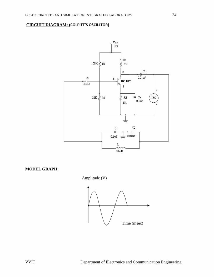
CIRCUIT DIAGRAM: (COLPITT’S OSCILLTOR)
MODEL GRAPH:
Amplitude (V)
Time (msec)
EC6411 CIRCUITS AND SIMULATION INTEGRATED LABORATORY 34
VVIT Department of Electronics and Communication Engineering
CIRCUIT DIAGRAM: (COLPITT’S OSCILLTOR)
MODEL GRAPH:
Amplitude (V)
Time (msec)
EC6411 CIRCUITS AND SIMULATION INTEGRATED LABORATORY 34
VVIT Department of Electronics and Communication Engineering
CIRCUIT DIAGRAM: (COLPITT’S OSCILLTOR)
MODEL GRAPH:
Amplitude (V)
Time (msec)
EC6411 CIRCUITS AND SIMULATION INTEGRATED LABORATORY 35
VVIT Department of Electronics and Communication Engineering
Ex. No: 6 COLPITT’S OSCILLTORDate:
AIM:
To design and construct a Colpitt’s oscillator for the given specifications C1= 0.1 F,
L=10mH, f=20 KHz, VCC=12V,IC=3mA, S=12.
APPARATUS REQUIRED:
S. No APPARATUS RANGE QUANTITY
1 Resistors 2k,1K,100 k, 22k Each One
2 RPS (0-30)V 1
3 Transistor BC107 1
4 Capacitors 0.1F, 0.01F
0.01F
Each 2
25 Inductor 10mH 1
6 CRO (0-30)MHz 1
7 Bread board - 1
8 Connectingwires
- few
Design of feedback Network:
Given C1= 0.1 F, C2= 0.01 F, L=10mH, f=20 KHz, VCC=12V.
Frequency Formula:
F = 1/ 2П LCeq , Where21
21
CC
CCCeq
F = (1 / 2П)21
21
CLC
CC , C2= 0.01F
EC6411 CIRCUITS AND SIMULATION INTEGRATED LABORATORY 36
VVIT Department of Electronics and Communication Engineering
TABULATION:
Amplitude(V) Time( msec ) Frequency(Hz)
EC6411 CIRCUITS AND SIMULATION INTEGRATED LABORATORY 37
VVIT Department of Electronics and Communication Engineering
THEORY:
Colpitt’s oscillator is very popular and is commonly used as local oscillator in radio
receivers. The collector voltage is applied to the collector through inductor L whose reactance
is high compared with X2 and may therefore be omitted from equivalent circuit, at zero
frequency. The circuit operates as Class C. the tuned circuit determines basically the frequency
of oscillation.
PROCEDURE:
1. Connect the circuit as per the circuit diagram.
2. Set VCC = 12V.
3. For the given supply the amplitude and time period is measured from CRO.
4. Frequency of oscillation is calculated by the formula f=1/T
5. Amplitude Vs time graph is drawn.
RESULT:
Thus the colpitt’s oscillator is designed and constructed for the given frequency.
Frequency :
EC6411 CIRCUITS AND SIMULATION INTEGRATED LABORATORY 38
VVIT Department of Electronics and Communication Engineering
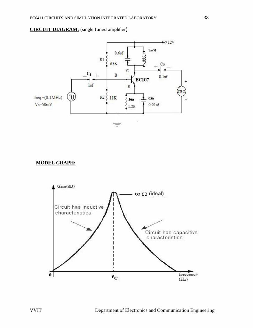
CIRCUIT DIAGRAM: (single tuned amplifier)
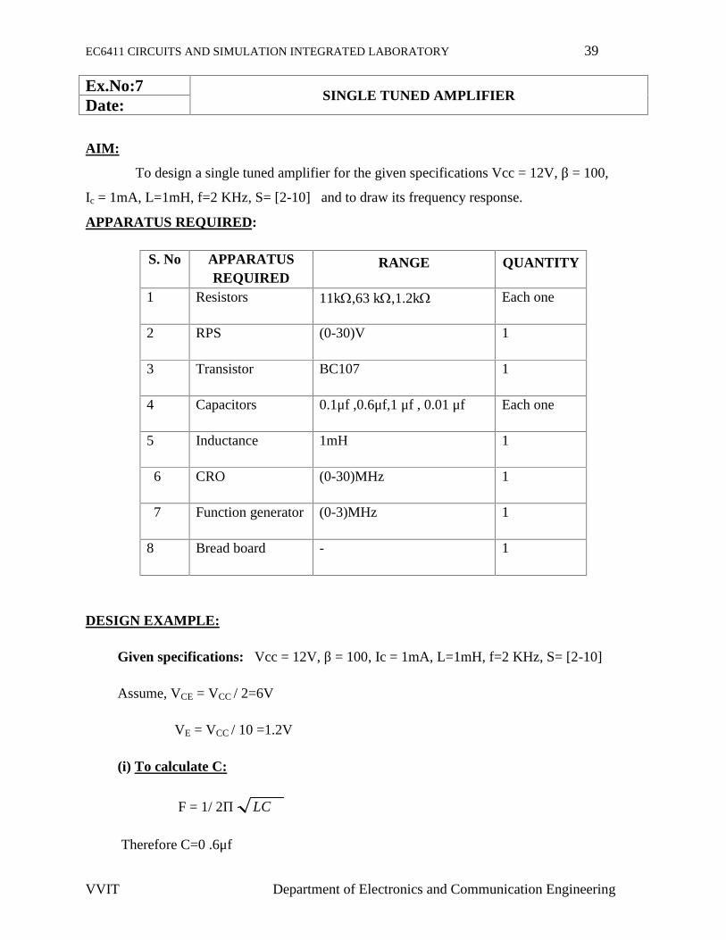
MODEL GRAPH:
EC6411 CIRCUITS AND SIMULATION INTEGRATED LABORATORY 38
VVIT Department of Electronics and Communication Engineering
CIRCUIT DIAGRAM: (single tuned amplifier)
MODEL GRAPH:
EC6411 CIRCUITS AND SIMULATION INTEGRATED LABORATORY 38
VVIT Department of Electronics and Communication Engineering
CIRCUIT DIAGRAM: (single tuned amplifier)
MODEL GRAPH:
EC6411 CIRCUITS AND SIMULATION INTEGRATED LABORATORY 39
VVIT Department of Electronics and Communication Engineering
Ex.No:7SINGLE TUNED AMPLIFIER
Date:
AIM:
To design a single tuned amplifier for the given specifications Vcc = 12V, β = 100,
Ic = 1mA, L=1mH, f=2 KHz, S= [2-10] and to draw its frequency response.
APPARATUS REQUIRED:
S. No APPARATUSREQUIRED
RANGE QUANTITY
1 Resistors 11k,63 k,1.2k Each one
2 RPS (0-30)V 1
3 Transistor BC107 1
4 Capacitors 0.1μf ,0.6μf,1 μf , 0.01 μf Each one
5 Inductance 1mH 1
6 CRO (0-30)MHz 1
7 Function generator (0-3)MHz 1
8 Bread board - 1
DESIGN EXAMPLE:
Given specifications: Vcc = 12V, β = 100, Ic = 1mA, L=1mH, f=2 KHz, S= [2-10]
Assume, VCE = VCC / 2=6V
VE = VCC / 10 =1.2V
(i) To calculate C:
F = 1/ 2П LC
Therefore C=0 .6μf
EC6411 CIRCUITS AND SIMULATION INTEGRATED LABORATORY 40
VVIT Department of Electronics and Communication Engineering
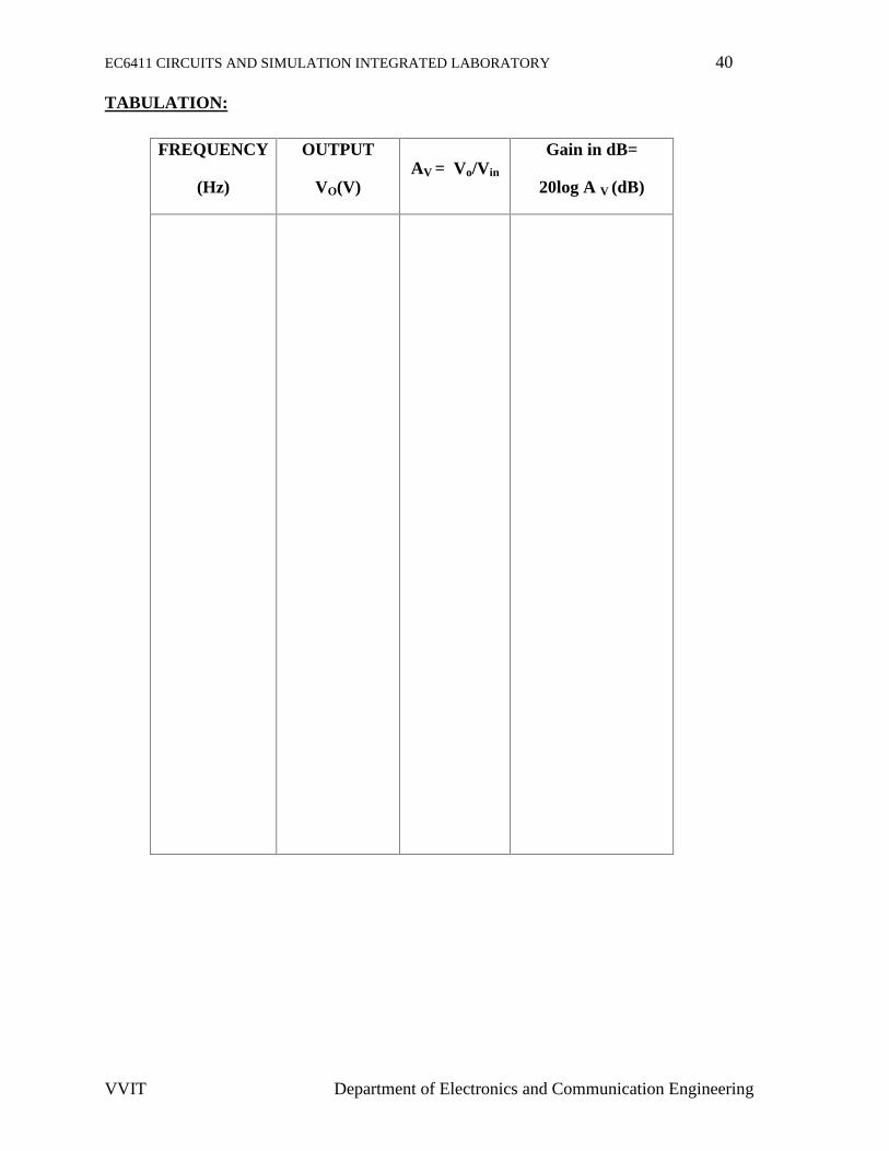
TABULATION:
FREQUENCY
(Hz)
OUTPUT
VO(V)AV = Vo/Vin
Gain in dB=
20log A V (dB)
EC6411 CIRCUITS AND SIMULATION INTEGRATED LABORATORY 41
VVIT Department of Electronics and Communication Engineering
(ii) To calculate RE:
The voltage drop across emitter resistance is given as ,
VE= IE RE , Where (IC~ IE)
RE = VE / IE= 1.2 / 1x10-3 = 1.2K
Assume S= 10, S= 1+ (RB / RE) & So, RB= 10.8 K
(iii) To find R1 & R2:
RB = R1 || R2
RB= R1 R2 / R1+ R2 ------------- (1)
By applying voltage divider rule,
VB= VCC x (R2 / R1+ R2) ------ (2)
From equation 1 & 2
RB / R1 = VB/ VCC --------------- (3)
VB = VBE + VE (VBE= 0.7 for silicon transistor)
VB= 0.7 + 1.2 = 1.9V
Substitute values in equation 3, R1 = 63K
From equation 2, R2= 11K≈ 10K
(iv) To calculate coupling capacitors:
(i)Input capacitance (Ci):
XCi = [hie + (1+ hfe) RE] || RB /10 (OR) RB /10
XCi = 10.8k/10=1.08k
XCi = 1/ 2ПfCi
Therefore Ci = 0.7 μf ≈ 1μf
EC6411 CIRCUITS AND SIMULATION INTEGRATED LABORATORY 42
VVIT Department of Electronics and Communication Engineering
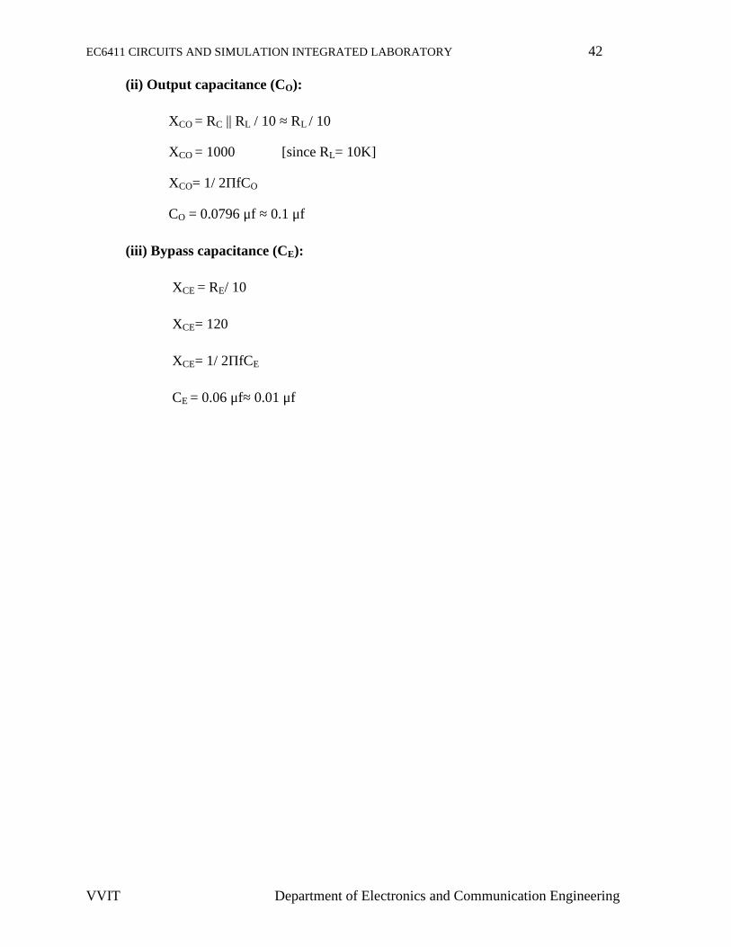
(ii) Output capacitance (CO):
XCO = RC || RL / 10 ≈ RL / 10
XCO = 1000 [since RL= 10K]
XCO= 1/ 2ПfCO
CO = 0.0796 μf ≈ 0.1 μf
(iii) Bypass capacitance (CE):
XCE = RE/ 10
XCE= 120
XCE= 1/ 2ПfCE
CE = 0.06 μf≈ 0.01 μf
EC6411 CIRCUITS AND SIMULATION INTEGRATED LABORATORY 43
VVIT Department of Electronics and Communication Engineering
THEORY:
The single tuned amplifier selecting the range of frequency the resistance load
replaced by the tank circuit. Tank circuit is nothing but inductors and capacitor in parallel with
each other. The tuned amplifier gives the response only at particular frequency at which the
output is almost zero. The resistor R1 and R2 provide potential diving biasing, Re and Ce
provide the thermal stabilization. This it fixes up the operating point.
PROCEDURE:
1. Connections are given as per the circuit diagram
2. By varying the frequency, amplitude is noted down
3. Gain is calculated in dB
4. Frequency response curve is drawn.
RESULT:
Thus the class – C single tuned amplifier is designed and frequency response is plotted.
EC6411 CIRCUITS AND SIMULATION INTEGRATED LABORATORY 44
VVIT Department of Electronics and Communication Engineering
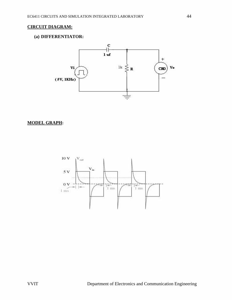
CIRCUIT DIAGRAM:
(a) DIFFERENTIATOR:
MODEL GRAPH:
EC6411 CIRCUITS AND SIMULATION INTEGRATED LABORATORY 44
VVIT Department of Electronics and Communication Engineering
CIRCUIT DIAGRAM:
(a) DIFFERENTIATOR:
MODEL GRAPH:
EC6411 CIRCUITS AND SIMULATION INTEGRATED LABORATORY 44
VVIT Department of Electronics and Communication Engineering
CIRCUIT DIAGRAM:
(a) DIFFERENTIATOR:
MODEL GRAPH:
EC6411 CIRCUITS AND SIMULATION INTEGRATED LABORATORY 45
VVIT Department of Electronics and Communication Engineering
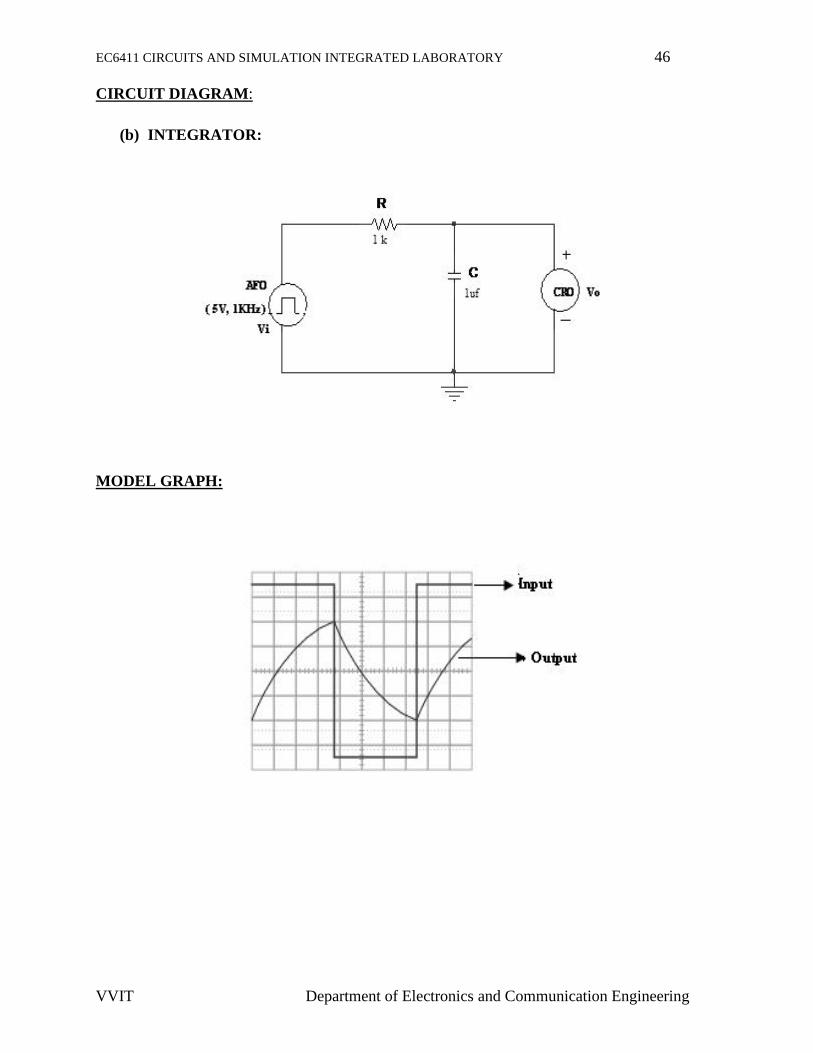
Ex. No: 8INTEGRATOR AND DIFFERENTIATOR
Date:
AIM:
To design and construct, differentiator and integrator circuit.
APPARATUS REQUIRED:
THEORY:
Differentiator:
Differentiator is a circuit which differentiates the input signal, it allows highorder frequency and blocks low order frequency. If time constant is very low it acts as adifferentiator. In this circuit input is continuous pulse with high and low value.
Integrator:In a low pass filter when the time constant is very large it acts as an
integrator. In this the voltage drop across C will be very small in comparison with the dropacross resistor R. Therefore, the total input appears across the R.
PROCEDURE:
1. Connections are given as per the circuit diagram.
2. Set the signal voltage Vi (5V, 1KHz) in the function generator.
3. Observe the output waveform in the CRO.
4. Sketch the output waveform.
S. No. APPARATUSREQUIRED
RANGE QUANTITY
1. Function generator (0-3)MHz 1
2. CRO (0-30)MHz 1
3. Capacitor 1μf 1
4. Resistor 1KΩ 1
5. Bread board - 1
EC6411 CIRCUITS AND SIMULATION INTEGRATED LABORATORY 46
VVIT Department of Electronics and Communication Engineering
CIRCUIT DIAGRAM:
(b) INTEGRATOR:
MODEL GRAPH:
EC6411 CIRCUITS AND SIMULATION INTEGRATED LABORATORY 46
VVIT Department of Electronics and Communication Engineering
CIRCUIT DIAGRAM:
(b) INTEGRATOR:
MODEL GRAPH:
EC6411 CIRCUITS AND SIMULATION INTEGRATED LABORATORY 46
VVIT Department of Electronics and Communication Engineering
CIRCUIT DIAGRAM:
(b) INTEGRATOR:
MODEL GRAPH:
EC6411 CIRCUITS AND SIMULATION INTEGRATED LABORATORY 47
VVIT Department of Electronics and Communication Engineering
RESULT:
Thus the integrator and differentiator circuit is constructed and output waveform is
observed.
EC6411 CIRCUITS AND SIMULATION INTEGRATED LABORATORY 48
VVIT Department of Electronics and Communication Engineering
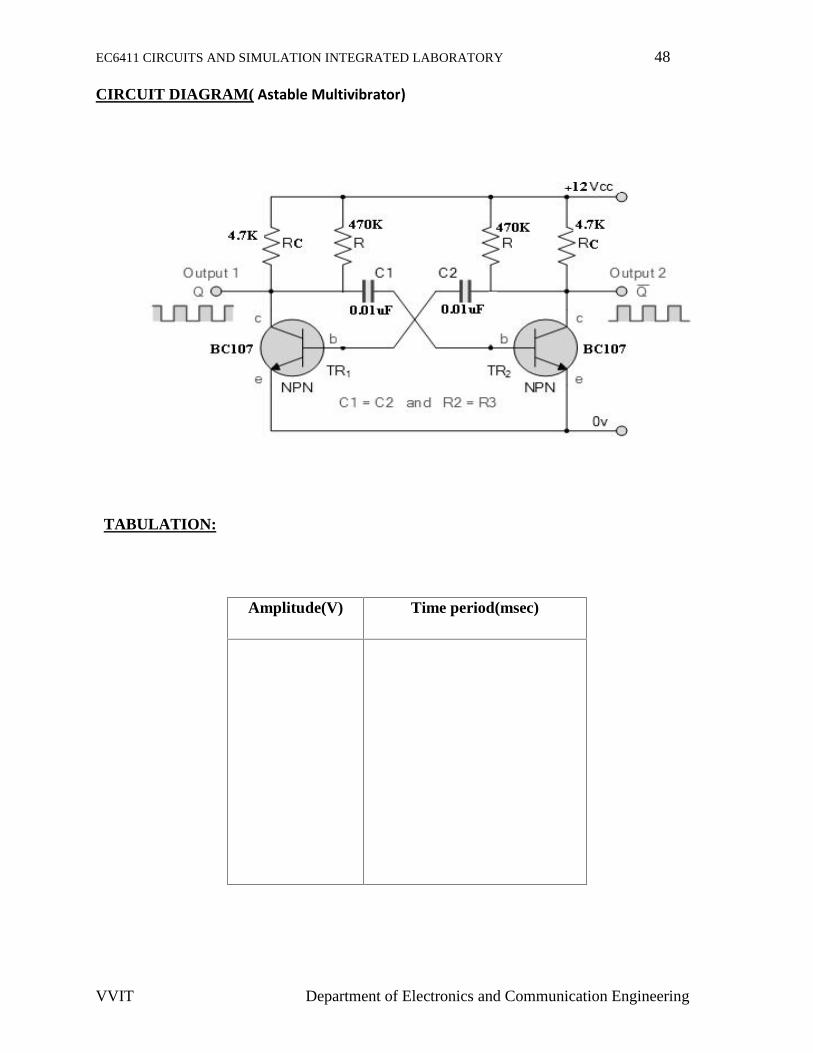
CIRCUIT DIAGRAM( Astable Multivibrator)
TABULATION:
Amplitude(V) Time period(msec)
EC6411 CIRCUITS AND SIMULATION INTEGRATED LABORATORY 48
VVIT Department of Electronics and Communication Engineering
CIRCUIT DIAGRAM( Astable Multivibrator)
TABULATION:
Amplitude(V) Time period(msec)
EC6411 CIRCUITS AND SIMULATION INTEGRATED LABORATORY 48
VVIT Department of Electronics and Communication Engineering
CIRCUIT DIAGRAM( Astable Multivibrator)
TABULATION:
Amplitude(V) Time period(msec)
EC6411 CIRCUITS AND SIMULATION INTEGRATED LABORATORY 49
VVIT Department of Electronics and Communication Engineering
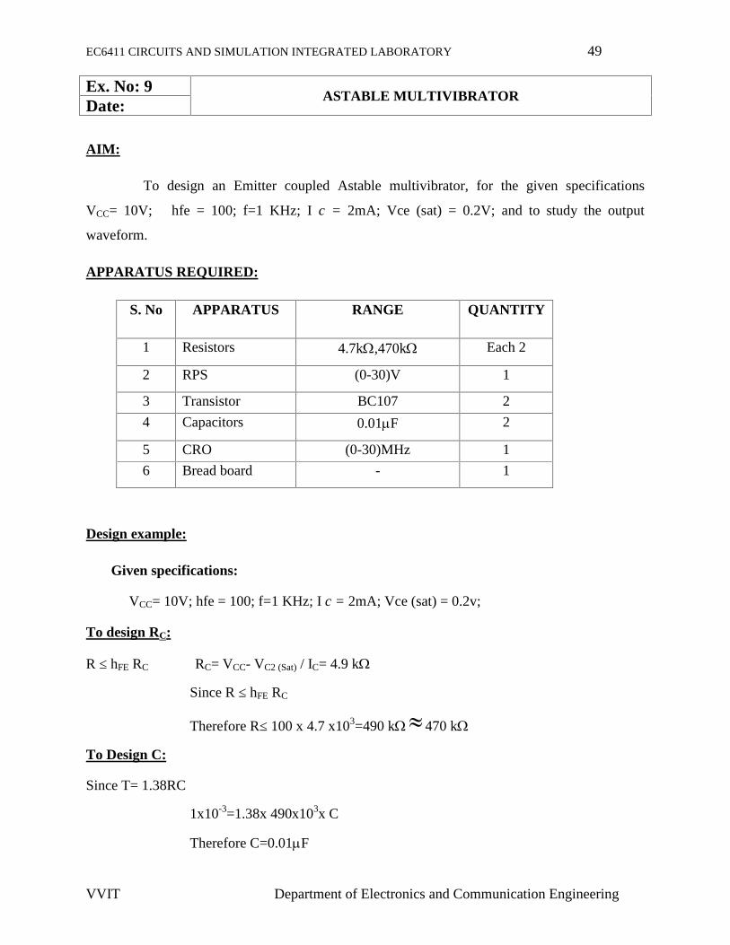
Ex. No: 9ASTABLE MULTIVIBRATOR
Date:
AIM:
To design an Emitter coupled Astable multivibrator, for the given specifications
VCC= 10V; hfe = 100; f=1 KHz; I c = 2mA; Vce (sat) = 0.2V; and to study the output
waveform.
APPARATUS REQUIRED:
S. No APPARATUS RANGE QUANTITY
1 Resistors 4.7k,470k Each 2
2 RPS (0-30)V 1
3 Transistor BC107 2
4 Capacitors 0.01F 2
5 CRO (0-30)MHz 1
6 Bread board - 1
Design example:
Given specifications:
VCC= 10V; hfe = 100; f=1 KHz; I c = 2mA; Vce (sat) = 0.2v;
To design RC:
R ≤ hFE RC RC= VCC- VC2 (Sat) / IC= 4.9 k
Since R ≤ hFE RC
Therefore R≤ 100 x 4.7 x103=490 k470 k
To Design C:
Since T= 1.38RC
1x10-3=1.38x 490x103x C
Therefore C=0.01F
EC6411 CIRCUITS AND SIMULATION INTEGRATED LABORATORY 50
VVIT Department of Electronics and Communication Engineering
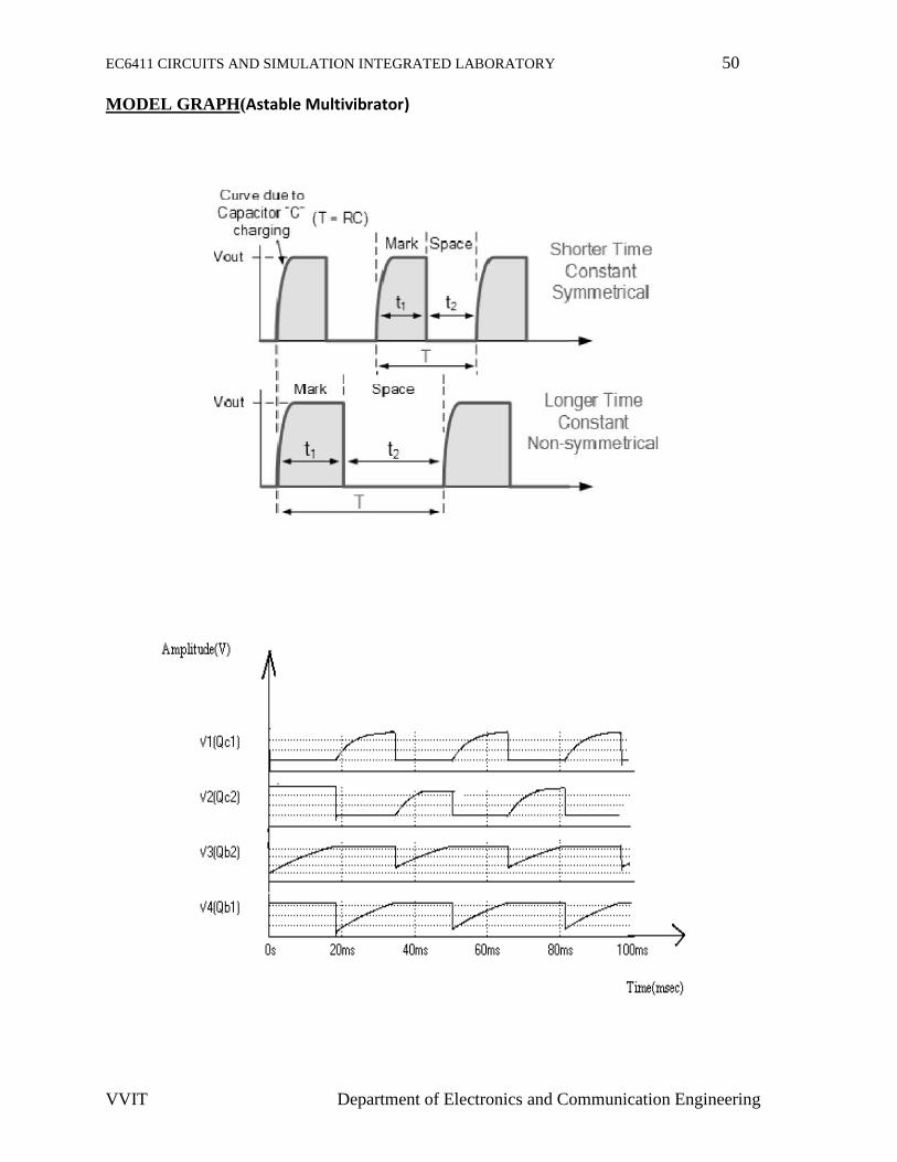
MODEL GRAPH(Astable Multivibrator)
EC6411 CIRCUITS AND SIMULATION INTEGRATED LABORATORY 50
VVIT Department of Electronics and Communication Engineering
MODEL GRAPH(Astable Multivibrator)
EC6411 CIRCUITS AND SIMULATION INTEGRATED LABORATORY 50
VVIT Department of Electronics and Communication Engineering
MODEL GRAPH(Astable Multivibrator)
EC6411 CIRCUITS AND SIMULATION INTEGRATED LABORATORY 51
VVIT Department of Electronics and Communication Engineering
THEORY:
The Astable multivibrator generates square wave without any external triggering pulse.
It has no stable state, i.e., it has two quasi- stable states. It switches back and forth from one
stable state to other, remaining in each state for a time depending upon the discharging of
a capacitive circuit. When supply voltage +Vcc is applied, one transistor will conduct more than
the other due to some circuit imbalance.
PROCEDURE:
1. Connect the circuit as per the circuit diagram.
2. Set VCC = 5V.
3. For the given supply the amplitude and time period is measured from CRO.
4. Frequency of oscillation is calculated by the formula f=1/T
5. Amplitude Vs time graph is drawn.
RESULT:
Thus the Astable Multivibrator is designed and output waveform is plotted.
EC6411 CIRCUITS AND SIMULATION INTEGRATED LABORATORY 52
VVIT Department of Electronics and Communication Engineering
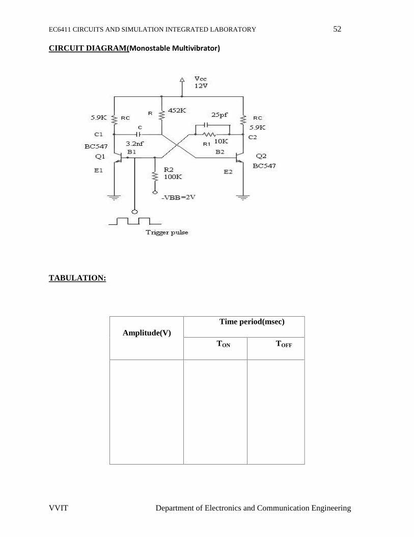
CIRCUIT DIAGRAM(Monostable Multivibrator)
TABULATION:
Amplitude(V)Time period(msec)
TON TOFF
EC6411 CIRCUITS AND SIMULATION INTEGRATED LABORATORY 52
VVIT Department of Electronics and Communication Engineering
CIRCUIT DIAGRAM(Monostable Multivibrator)
TABULATION:
Amplitude(V)Time period(msec)
TON TOFF
EC6411 CIRCUITS AND SIMULATION INTEGRATED LABORATORY 52
VVIT Department of Electronics and Communication Engineering
CIRCUIT DIAGRAM(Monostable Multivibrator)
TABULATION:
Amplitude(V)Time period(msec)
TON TOFF
EC6411 CIRCUITS AND SIMULATION INTEGRATED LABORATORY 53
VVIT Department of Electronics and Communication Engineering
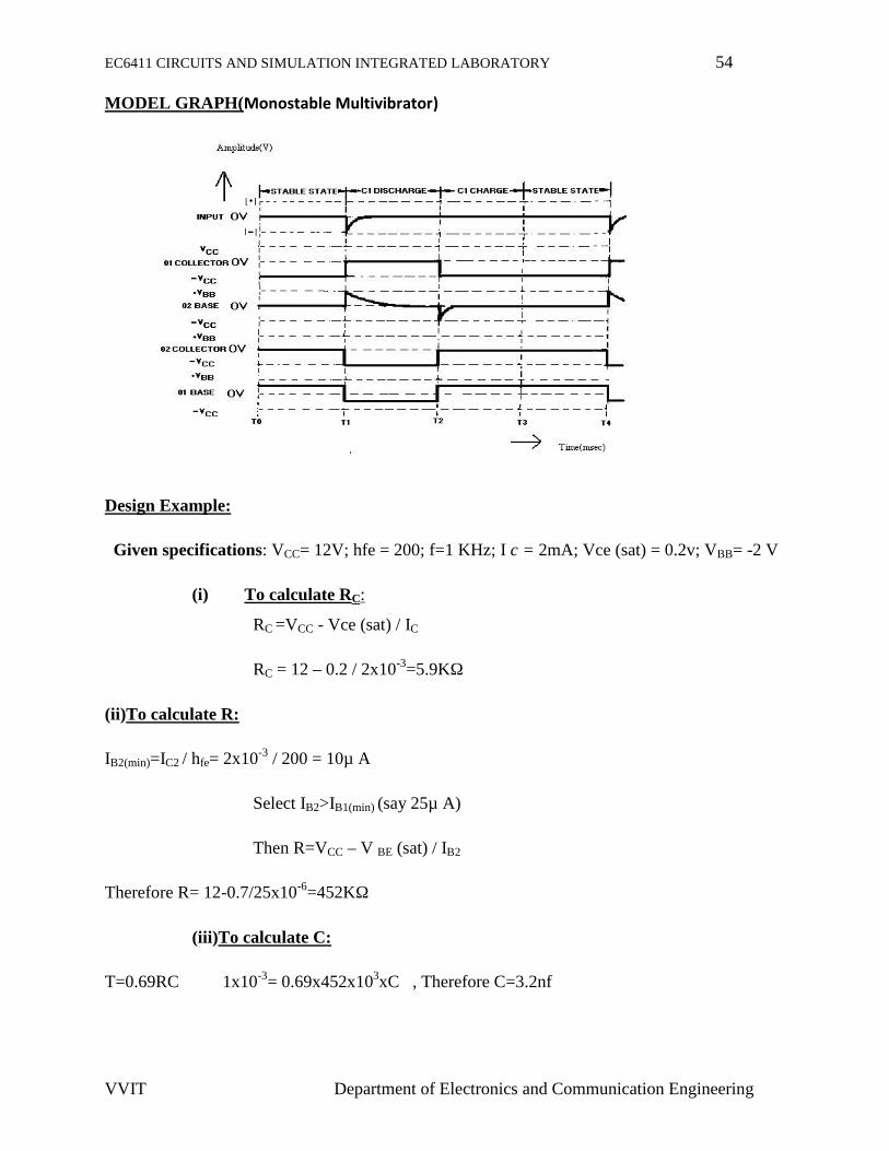
Ex. No: 10MONOSTABLE MULTIVIBRATOR
Date:
AIM:
To design and test the performance of Monostable Multivibrator for the given
specifications VCC= 12V; hfe = 200; f=1 KHz; Ic = 2mA; Vce (sat) = 0.2v; VBB= - 2V and to
obtain its output waveform.
APPARATUS REQUIRED:
S.No APPARATUS RANGE QUANTITY
1Resistors 5.9 k,452 k,100
k,10K
2,1,1,1
2 RPS (0-30)V 1
3 Transistor BC547 2
4 CRO (0-30)MHz 1
5 Capacitor 3.2nf,25pf Each One
6 Bread board - 1
To calculate R1 & R2:
VB1= (VBB R1/ R1 +R2) + (VCE (sat) R2 / R1+R2)
Since Q1 is in off state, VB1 ≤ 0
Then (VBB R1/ R1 +R2) = (VCE (sat) R2 / R1+R2)
VBB R1 = VCE (sat) R2
2 R1 = 0.2 R2
Assume R1=10KΩ, then R2=100 KΩ
Consider, C1= 25pf (commutative capacitor)
EC6411 CIRCUITS AND SIMULATION INTEGRATED LABORATORY 54
VVIT Department of Electronics and Communication Engineering
MODEL GRAPH(Monostable Multivibrator)
Design Example:
Given specifications: VCC= 12V; hfe = 200; f=1 KHz; I c = 2mA; Vce (sat) = 0.2v; VBB= -2 V
(i) To calculate RC:
RC =VCC - Vce (sat) / IC
RC = 12 – 0.2 / 2x10-3=5.9KΩ
(ii)To calculate R:
IB2(min)=IC2 / hfe= 2x10⁻³ / 200 = 10µ A
Select IB2>IB1(min) (say 25µ A)
Then R=VCC – V BE (sat) / IB2
Therefore R= 12-0.7/25x10-6=452KΩ
(iii)To calculate C:
T=0.69RC 1x10-3= 0.69x452x103xC , Therefore C=3.2nf
EC6411 CIRCUITS AND SIMULATION INTEGRATED LABORATORY 55
VVIT Department of Electronics and Communication Engineering
THEORY:
The Monostable multivibrator has one stable state when an external trigger input is
applied the circuit changes its state from stable to quasi -stable state. And then automatically
after some time interval the circuit returns back to the original normal stable state. The time T is
dependent on circuit components.
The capacitor C1 is a speed-up capacitor coupled to base of Q2 through C. Thus
DC coupling in Bistable multivibrator is replaced by a capacitor coupling. The resistor R, at
input of Q2 is returned to VCC.
The value of R2, V BB are chosen such that transistor Q1 is off by reverse biasing it. Q2 is on.
This is possible by forward biasing Q2 with the help of VCC and resistance R. Thus Q2-ON and
Q1-OFF is normal stable state of circuit.
PROCEDURE:
1. Connect the circuit as per the circuit diagram.
2. Give a negative trigger input to the base of Q1.
3. Note the output of transistor Q2 and Q1.
4. Find the value of Ton and Toff.
5. Plot the response of the Monostable Multivibrator
RESULT:
Thus the Monostable Multivibrator is designed and the performance is verified.
Theoretical period :
Practical period :
EC6411 CIRCUITS AND SIMULATION INTEGRATED LABORATORY 56
VVIT Department of Electronics and Communication Engineering
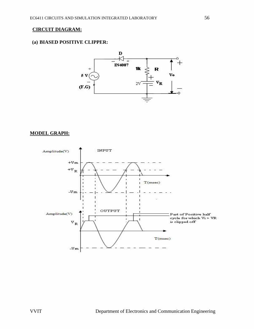
CIRCUIT DIAGRAM:
(a) BIASED POSITIVE CLIPPER:
MODEL GRAPH:
EC6411 CIRCUITS AND SIMULATION INTEGRATED LABORATORY 56
VVIT Department of Electronics and Communication Engineering
CIRCUIT DIAGRAM:
(a) BIASED POSITIVE CLIPPER:
MODEL GRAPH:
EC6411 CIRCUITS AND SIMULATION INTEGRATED LABORATORY 56
VVIT Department of Electronics and Communication Engineering
CIRCUIT DIAGRAM:
(a) BIASED POSITIVE CLIPPER:
MODEL GRAPH:
EC6411 CIRCUITS AND SIMULATION INTEGRATED LABORATORY 57
VVIT Department of Electronics and Communication Engineering
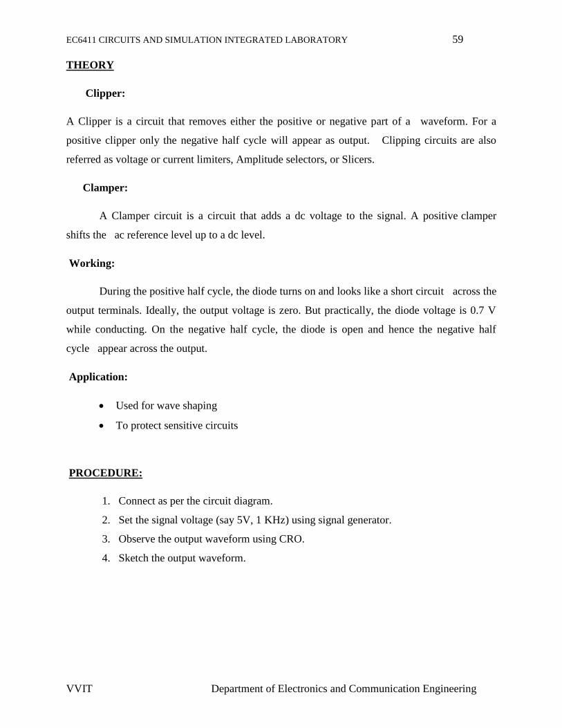
Ex. No: 11CLIPPER AND CLAMPER CIRCUITS
Date:
AIM:
To construct and design the clipper and clamper circuits using diodes at 1 KHz
APPARATUS REQUIRED:
S.No APPARATUS RANGE QUANTITY
1 Resistors 1 k 1
2 RPS (0-30)V 1
3 Diode IN4007 1
4 CRO (0-30)MHz 1
6 Function generator (0-3)MHz 1
7 Capacitor 1 μf 2
8 Bread board - 1
DESIGN:
Given f=1 kHz,
T=t=1/f=1x10-3 sec=RC
Assume, C=1uF
Then, R=1K
EC6411 CIRCUITS AND SIMULATION INTEGRATED LABORATORY 58
VVIT Department of Electronics and Communication Engineering
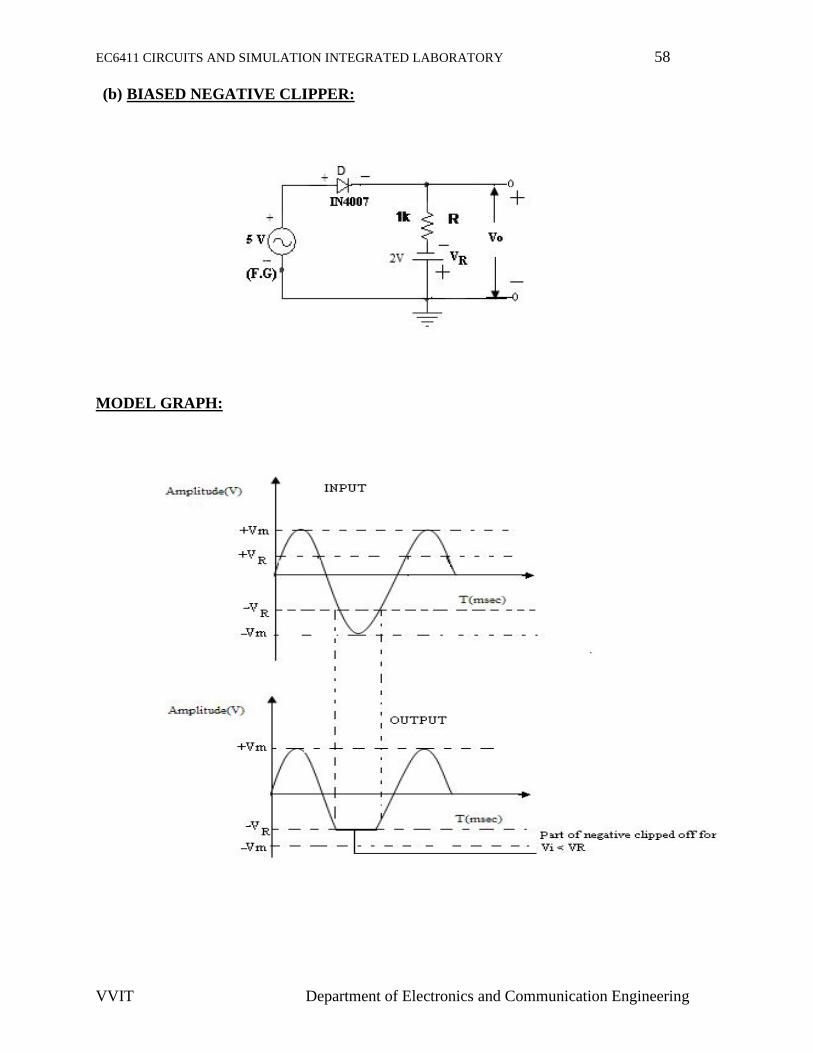
(b) BIASED NEGATIVE CLIPPER:
MODEL GRAPH:
EC6411 CIRCUITS AND SIMULATION INTEGRATED LABORATORY 58
VVIT Department of Electronics and Communication Engineering
(b) BIASED NEGATIVE CLIPPER:
MODEL GRAPH:
EC6411 CIRCUITS AND SIMULATION INTEGRATED LABORATORY 58
VVIT Department of Electronics and Communication Engineering
(b) BIASED NEGATIVE CLIPPER:
MODEL GRAPH:
EC6411 CIRCUITS AND SIMULATION INTEGRATED LABORATORY 59
VVIT Department of Electronics and Communication Engineering
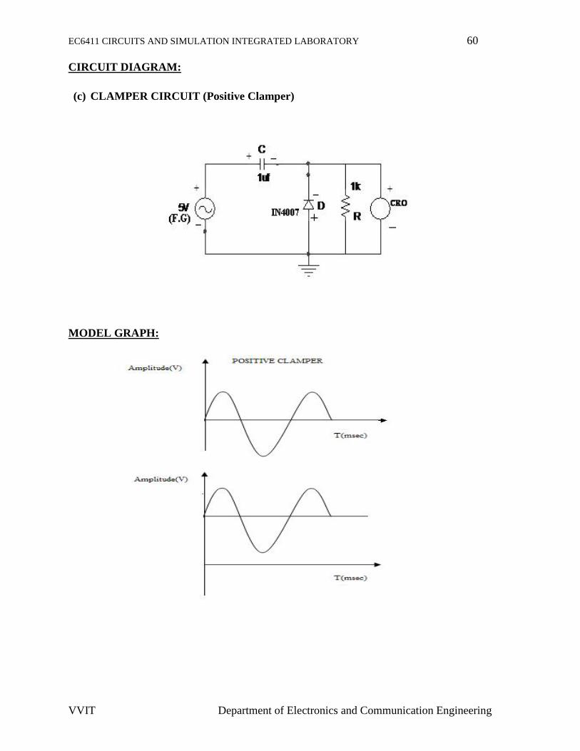
THEORY
Clipper:
A Clipper is a circuit that removes either the positive or negative part of a waveform. For a
positive clipper only the negative half cycle will appear as output. Clipping circuits are also
referred as voltage or current limiters, Amplitude selectors, or Slicers.
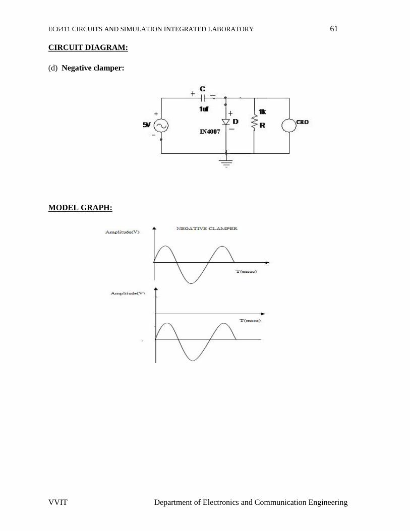
Clamper:
A Clamper circuit is a circuit that adds a dc voltage to the signal. A positive clamper
shifts the ac reference level up to a dc level.
Working:
During the positive half cycle, the diode turns on and looks like a short circuit across the
output terminals. Ideally, the output voltage is zero. But practically, the diode voltage is 0.7 V
while conducting. On the negative half cycle, the diode is open and hence the negative half
cycle appear across the output.
Application:
Used for wave shaping
To protect sensitive circuits
PROCEDURE:
1. Connect as per the circuit diagram.
2. Set the signal voltage (say 5V, 1 KHz) using signal generator.
3. Observe the output waveform using CRO.
4. Sketch the output waveform.
EC6411 CIRCUITS AND SIMULATION INTEGRATED LABORATORY 60
VVIT Department of Electronics and Communication Engineering
CIRCUIT DIAGRAM:
(c) CLAMPER CIRCUIT (Positive Clamper)
MODEL GRAPH:
EC6411 CIRCUITS AND SIMULATION INTEGRATED LABORATORY 60
VVIT Department of Electronics and Communication Engineering
CIRCUIT DIAGRAM:
(c) CLAMPER CIRCUIT (Positive Clamper)
MODEL GRAPH:
EC6411 CIRCUITS AND SIMULATION INTEGRATED LABORATORY 60
VVIT Department of Electronics and Communication Engineering
CIRCUIT DIAGRAM:
(c) CLAMPER CIRCUIT (Positive Clamper)
MODEL GRAPH:
EC6411 CIRCUITS AND SIMULATION INTEGRATED LABORATORY 61
VVIT Department of Electronics and Communication Engineering
CIRCUIT DIAGRAM:
(d) Negative clamper:
MODEL GRAPH:
EC6411 CIRCUITS AND SIMULATION INTEGRATED LABORATORY 61
VVIT Department of Electronics and Communication Engineering
CIRCUIT DIAGRAM:
(d) Negative clamper:
MODEL GRAPH:
EC6411 CIRCUITS AND SIMULATION INTEGRATED LABORATORY 61
VVIT Department of Electronics and Communication Engineering
CIRCUIT DIAGRAM:
(d) Negative clamper:
MODEL GRAPH:
EC6411 CIRCUITS AND SIMULATION INTEGRATED LABORATORY 62
VVIT Department of Electronics and Communication Engineering
RESULT:
Thus, the output waveforms for Clipper and Clamper circuits were observed.
EC6411 CIRCUITS AND SIMULATION INTEGRATED LABORATORY 63
VVIT Department of Electronics and Communication Engineering
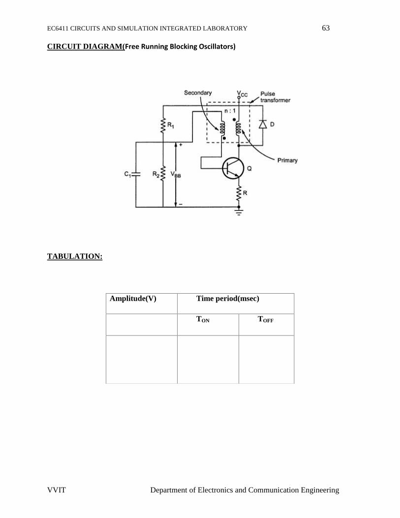
CIRCUIT DIAGRAM(Free Running Blocking Oscillators)
TABULATION:
Amplitude(V) Time period(msec)
TON TOFF
EC6411 CIRCUITS AND SIMULATION INTEGRATED LABORATORY 64
VVIT Department of Electronics and Communication Engineering
Ex. No: 12FREE RUNNING BLOCKING OSCILLATORS
Date:
AIM:
To design and test the performance of free running blocking oscillator and to obtain its
output waveform.
APPARATUS REQUIRED:
S. NoAPPARATUS
REQUIREDRANGE QUANTITY
1 Resistors 100 k,10K 2,1
2 RPS (0-30)V 1
3 Transistor BC547 2
4 CRO (0-30)MHz 1
5 Capacitor 25pf 1
6 Transformer 6V-0-6V 1
7 Diode 1N4001 1
8 Bread board - 1
EC6411 CIRCUITS AND SIMULATION INTEGRATED LABORATORY 65
VVIT Department of Electronics and Communication Engineering
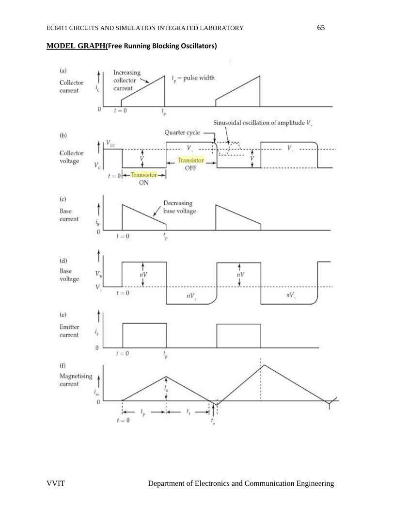
MODEL GRAPH(Free Running Blocking Oscillators)
EC6411 CIRCUITS AND SIMULATION INTEGRATED LABORATORY 66
VVIT Department of Electronics and Communication Engineering
THEORY:
Astable blocking oscillator is also called free running blocking oscillator. It produces
train of pulses, when triggered. The pulse width and the duty cycle of the blocking oscillator
output can be controlled as per the requirement. There are two types of blockling oscillators
available, which are,
1. Diode controlled Astable blocking oscillator.
2. RC controlled Astable blocking oscillator.
Applications:
1. Both Monostable and Astable blocking oscillators are used for generating pulses of
large peak power.
2. It is used as a frequency divider or counter.
3. It is used to discharge a capacitor rapidly.
4. It may be used as a gating waveform with very small mark space ratio.
5. Both positive and negative pulses can be obtained from a blocking oscillator by using a
tertiary winding.
PROCEDURE:
1. Connect the circuit as per the circuit diagram.
2. Note down the voltages and current at various base, emitter and collector.
3. Note the magnetizing current.
4. Draw the waveform for various values.
RESULT:
Thus the free running blocking oscillator is designed and the performance is verified.
EC6411 CIRCUITS AND SIMULATION INTEGRATED LABORATORY 67
VVIT Department of Electronics and Communication Engineering
SIMULATION USING PSPICE
(Using Transistor)
EC6411 CIRCUITS AND SIMULATION INTEGRATED LABORATORY 68
VVIT Department of Electronics and Communication Engineering
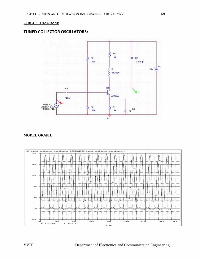
CIRCUIT DIAGRAM:
TUNED COLLECTOR OSCILLATORS:
MODEL GRAPH:
EC6411 CIRCUITS AND SIMULATION INTEGRATED LABORATORY 69
VVIT Department of Electronics and Communication Engineering
Ex. No: 13TUNED COLLECTOR OSCILLATORS
Date:
AIM:
To simulate a tuned collector oscillation circuit using PSPICE
APPARATUS REQUIRED:
1. PC
2. PSPICE software
THEORY:
Tuned collector oscillator is a type of transistor LC oscillator where the tuned circuit
(tank) consists of a transformer and a capacitor is connected in the collector circuit of the
transistor. Tuned collector oscillator is of course the simplest and the basic type of LC
oscillators. The tuned circuit connected at the collector circuit behaves like a purely resistive
load at resonance and determines the oscillator frequency. The common applications of tuned
collector oscillator are RF oscillator circuits, mixers, frequency demodulators, signal generators
etc.
PROCEDURE:
1. Click on the start menu and select the Pspice simulation software
2. Select the parts required for the circuit from the parts menu and
place them in the work space
3. Connect the parts using wires
4. Save the file and select the appropriate analysis
5. Simulate the circuit and observe the corresponding output
waveforms
RESULT:
Thus, the tuned collector oscillator circuit is simulated using Pspice.
EC6411 CIRCUITS AND SIMULATION INTEGRATED LABORATORY 70
VVIT Department of Electronics and Communication Engineering
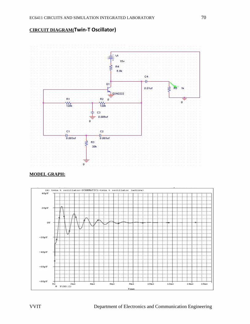
CIRCUIT DIAGRAM(Twin-T Oscillator)
MODEL GRAPH:
EC6411 CIRCUITS AND SIMULATION INTEGRATED LABORATORY 71
VVIT Department of Electronics and Communication Engineering
Ex. No: 14TWIN-T OSCILLATOR
Date:
AIM:
To simulate a twin-T oscillation circuit using PSPICE
APPARATUS REQUIRED:
1. PC
2. PSPICE software
THEORY:
"Twin-T" oscillator uses two "T" RC circuits operated in parallel. One circuit is an R-C-R
"T" which acts as a low-pass filter. The second circuit is a C-R-C "T" which operates as a high-
pass filter. Together, these circuits form a bridge which is tuned at the desired frequency of
oscillation. The signal in the C-R-C branch of the Twin-T filter is advanced, in the R-C-R -
delayed, so they may cancel one another for frequency f=12πRC if x=2; if it is connected as a
negative feedback to an amplifier, and x>2, the amplifier becomes an oscillator.
PROCEDURE:
1. Click on the start menu and select the Pspice simulation software
2. Select the parts required for the circuit from the parts menu and
place them in the work space
3. Connect the parts using wires
4. Save the file and select the appropriate analysis
5. Simulate the circuit and observe the corresponding output
waveforms
RESULT:
Thus, the twin-T oscillator oscillator circuit is simulated using Pspice.
EC6411 CIRCUITS AND SIMULATION INTEGRATED LABORATORY 72
VVIT Department of Electronics and Communication Engineering
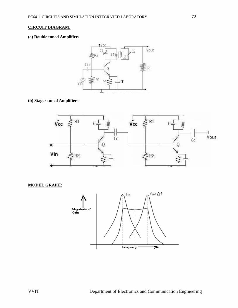
CIRCUIT DIAGRAM:
(a) Double tuned Amplifiers
(b) Stager tuned Amplifiers
MODEL GRAPH:
EC6411 CIRCUITS AND SIMULATION INTEGRATED LABORATORY 73
VVIT Department of Electronics and Communication Engineering
Ex. No: 15DOUBLE AND STAGER TUNED AMPLIFIERS
Date:
AIM:To simulate a double and stager tuned amplifiers circuit using PSPICE
APPARATUS REQUIRED:
1. PC
2. PSPICE software
THEORY:
Stagger Tuned Amplifiers are used to improve the overall frequency response of tuned
Amplifiers. Stagger tuned Amplifiers are usually designed so that the overall response exhibits
maximal flatness around the centre frequency. It needs a number of tuned circuits operating in
union. The overall frequency response of a Stagger tuned amplifier is obtained by adding the
individual response together. Since the resonant Frequencies of different tuned circuits are
displaced or staggered, they are referred as stagger tuned amplifier.
PROCEDURE:
1. Click on the start menu and select the Pspice simulation software
2. Select the parts required for the circuit from the parts menu and
place them in the work space
3. Connect the parts using wires
4. Save the file and select the appropriate analysis
5. Simulate the circuit and observe the corresponding output
waveforms
RESULT:
Thus, the double and stager tuned amplifier circuit is simulated using Pspice.
EC6411 CIRCUITS AND SIMULATION INTEGRATED LABORATORY 74
VVIT Department of Electronics and Communication Engineering
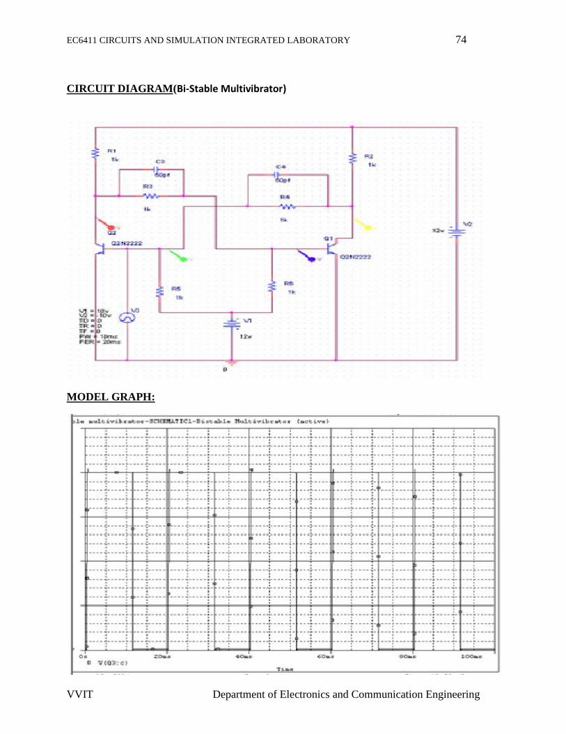
CIRCUIT DIAGRAM(Bi-Stable Multivibrator)
MODEL GRAPH:
EC6411 CIRCUITS AND SIMULATION INTEGRATED LABORATORY 75
VVIT Department of Electronics and Communication Engineering
Ex. No: 16BI-STABLE MULTIVIBRATOR
Date:
AIM:
To simulate an Bi-stable multivibrator using PSPICE
APPARATUS REQUIRED:
1. PC
2. PSPICE software
THEORY:
Bi- stable multivibrator contains two stable states and no quasi states. It requires two
clock or trigger pulses to change the states. It is also called as flip flop, scale of two toggle
circuit, trigger circuit.
PROCEDURE:
1. Click on the start menu and select the Pspice simulation software
2. Select the parts required for the circuit from the parts menu and place
them in the work space
3. Connect the parts using wires
4. Save the file and select the appropriate analysis
5. Simulate the circuit and observe the corresponding output waveforms
APPLICATIONS:
It is used in digital operations like counting, storing data’s in flip flops
and production of square waveforms.
RESULT:
Thus, the Bi-stable multivibrator circuit is simulated using PSpice.
EC6411 CIRCUITS AND SIMULATION INTEGRATED LABORATORY 76
VVIT Department of Electronics and Communication Engineering
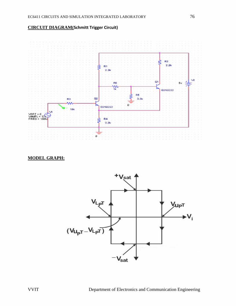
CIRCUIT DIAGRAM(Schmitt Trigger Circuit)
MODEL GRAPH:
EC6411 CIRCUITS AND SIMULATION INTEGRATED LABORATORY 76
VVIT Department of Electronics and Communication Engineering
CIRCUIT DIAGRAM(Schmitt Trigger Circuit)
MODEL GRAPH:
EC6411 CIRCUITS AND SIMULATION INTEGRATED LABORATORY 76
VVIT Department of Electronics and Communication Engineering
CIRCUIT DIAGRAM(Schmitt Trigger Circuit)
MODEL GRAPH:
EC6411 CIRCUITS AND SIMULATION INTEGRATED LABORATORY 77
VVIT Department of Electronics and Communication Engineering
Ex. No: 17 SCHMITT TRIGGER CIRCUIT WITH PREDICTABLEHYSTERESISDate:
AIM:
To simulate a schmitt trigger circuit with predictable hysteresis using PSPICE
APPARATUS REQUIRED:
1. PC
2. PSPICE software
THEORY:
A Schmitt trigger is a comparator circuit with hysteresis, implemented by applying
positive feedback to the non-inverting input of a comparator or differential amplifier. It is an
active circuit which converts an analog input signal to a digital output signal. The circuit is
named a "trigger" because the output retains its value until the input changes sufficiently to
trigger a change. In the non-inverting configuration, when the input is higher than a certain
chosen threshold, the output is high. When the input is below a different (lower) chosen
threshold, the output is low, and when the input is between the two levels, the output retains its
value. This dual threshold action is called hysteresis and implies that the Schmitt trigger
possesses memory and can act as a bistable circuit (latch or flip-flop). There is a close relation
between the two kinds of circuits: a Schmitt trigger can be converted into a latch and a latch can
be converted into a Schmitt trigger.
Schmitt trigger devices are typically used in signal conditioning applications to remove
noise from signals used in digital circuits, particularly mechanical switch bounce. They are also
used in closed loop negative feedback configurations to implement relaxation oscillators, used
in function generators and switching power supplies.
EC6411 CIRCUITS AND SIMULATION INTEGRATED LABORATORY 78
VVIT Department of Electronics and Communication Engineering
PROCEDURE:
1. Click on the start menu and select the Pspice simulation software
2. Select the parts required for the circuit from the parts menu and place
them in the work space
3. Connect the parts using wires
4. Save the file and select the appropriate analysis
5. Simulate the circuit and observe the corresponding output waveforms
RESULT:
Thus, the Bi-stable multivibrator circuit is simulated using PSpice.
EC6411 CIRCUITS AND SIMULATION INTEGRATED LABORATORY 79
VVIT Department of Electronics and Communication Engineering
CIRCUIT DIAGRAM(Mono Stable Multivibrator)
MODEL GRAPH:

EC6411 CIRCUITS AND SIMULATION INTEGRATED LABORATORY 80
VVIT Department of Electronics and Communication Engineering
Ex. No: 18MONO STABLE MULTIVIBRATOR
Date:
AIM:
To simulate an Monostable multivibrator circuit using PSPICE
APPARATUS REQUIRED:
1. PC
2. PSPICE software
THEORY:
Monostable multivibrator is an electronic circuit which has one stable state
and one quasi stable state. It needs external pulse to change their stable state to quasi state and
return back to its stable state after completing the time constant RC. Thus the RC time constant
determines the duration of quasi state. Also called as one-shot, single shot and one swing
multivibrator.
PROCEDURE:
1. Click on the start menu and select the Pspice simulation software
2. Select the parts required for the circuit from the parts menu and
place them in the work space
3. Connect the parts using wires
4. Save the file and select the appropriate analysis
5. Simulate the circuit and observe the corresponding output
waveforms
Applications:
Used as triggering circuit for some circuits like timer circuit, delay
circuits etc.
RESULT:
Thus, the Monostable Multivibrator circuit is simulated using Pspice.
EC6411 CIRCUITS AND SIMULATION INTEGRATED LABORATORY 81
VVIT Department of Electronics and Communication Engineering
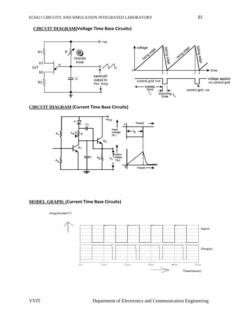
CIRCUIT DIAGRAM(Voltage Time Base Circuits)
CIRCUIT DIAGRAM (Current Time Base Circuits)
MODEL GRAPH: (Current Time Base Circuits)
EC6411 CIRCUITS AND SIMULATION INTEGRATED LABORATORY 81
VVIT Department of Electronics and Communication Engineering
CIRCUIT DIAGRAM(Voltage Time Base Circuits)
CIRCUIT DIAGRAM (Current Time Base Circuits)
MODEL GRAPH: (Current Time Base Circuits)
EC6411 CIRCUITS AND SIMULATION INTEGRATED LABORATORY 81
VVIT Department of Electronics and Communication Engineering
CIRCUIT DIAGRAM(Voltage Time Base Circuits)
CIRCUIT DIAGRAM (Current Time Base Circuits)
MODEL GRAPH: (Current Time Base Circuits)
EC6411 CIRCUITS AND SIMULATION INTEGRATED LABORATORY 82
VVIT Department of Electronics and Communication Engineering
Ex. No: 19VOLTAGE AND CURRENT TIME BASE CIRCUITS
Date:
AIM:
To simulate a voltage and current time base circuits using PSPICE
APPARATUS REQUIRED:
1. PC
2. PSPICE software
THEORY:
A voltage and current time base circuit is an electronic circuit which has one
stable state and one quasi stable state. It needs external pulse to change their stable state to quasi
state and return back to its stable state after completing the time constant RC. Thus the RC time
constant determines the duration of quasi state.
PROCEDURE:
1. Click on the start menu and select the Pspice simulation software
2. Select the parts required for the circuit from the parts menu and
place them in the work space
3. Connect the parts using wires
4. Save the file and select the appropriate analysis
5. Simulate the circuit and observe the corresponding output
waveforms
Applications:
Used as triggering circuit for some circuits like timer circuit, delay
circuits etc.
RESULT:
Thus, the voltage and current time base circuit is simulated using Pspice.


![Analysis and Design of a Low Noise Shunt-Shunt CMOS ... · The shunt-shunt TIA topology is shown in Fig. 1 [6]. This topology is composed by a voltage amplifier with a transfer function](https://img.pdfslide.net/doc/110x75/5ea54e44e44a2608a21306f1/analysis-and-design-of-a-low-noise-shunt-shunt-cmos-the-shunt-shunt-tia-topology.jpg)