Embed Size (px)
Citation preview
IEEE TRANSACTIONS ON BIOMEDICAL CIRCUITS AND SYSTEMS, VOL. 6, NO. 2, APRIL 2012 111
CMOS Low Current Measurement System forBiomedical Applications
Brian Goldstein, Graduate Student Member, IEEE, Dongsoo Kim, Member, IEEE, Jian Xu, T. Kyle Vanderlick, andEugenio Culurciello, Senior Member, IEEE
Abstract—We present a micro-chip implementation of a low cur-rent measurement system for biomedical applications using capac-itive feedback that exhibits 190 fA of RMS noise in a 1 kHz band-width. The sampling rate is selectable up to 100 kHz. When mea-suring the amplifier noise with a 10 G� resistor and a 47 pF capac-itor at the input, typical of cell membrane capacitance in DNA andpatch clamp experiments, the measured RMS noise was 2.44 pA ona 50 pA signal in a 10 kHz bandwidth. Two channels were imple-mented on 630 440 m� using a 0.5- m 3-metal 2-poly CMOSprocess. Each channel consumes 1.5 mW of power from a 3.3 Vsupply. We measured the characteristics of an artificial lipid bi-layer similar to the ones used in DNA sequencing experiments viananopores.
Index Terms—Amperometry, biomedical measurements, ca-pacitive feedback, current measurement, integrator, low currentmeasurement system, low noise circuit, noise analysis, potentio-stat, voltage-clamp.
I. INTRODUCTION
I NTEGRATED multichannel low-noise current mea-surement systems are becoming extremely important
components to interface and study physical phenomena at thesub-micro-scale for use in biological research and instrumen-tation. For example, patch-clamp is the electrophysiology goldstandard technique to measure ion-channel currents when thecell membrane is “clamped” to commanded voltages. A lowcurrent measurement system (LCMS) is required to study theeffect of drugs and medical treatments on ion channel dynamics[1], [2]. During single channel recording, the current level canbe as low as tens of pico-amperes in 1–10 kHz bandwidth witha 50 pF electrode capacitance.
Another application that requires an integrated low currentmeasurement system is a potential rapid DNA sequencing
Manuscript received July 22, 2011; revised November 02, 2011; acceptedDecember 15, 2011. Date of publication February 14, 2012; date of currentversion April 19, 2012. This paper was supported in part by NSF DBI1154498, ONR N00014-08-1-0065, N00014-08-1-1014, N0463A-11-P-0022,and NIH R01 NS06511. This paper was recommended by Associate Editor M.Stanacevic.
B. Goldstein is with the Department of Electrical Engineering, Yale Univer-sity, New Haven, CT 06520 USA (e-mail: [email protected]).
D. Kim was with the Department of Electrical Engineering, Yale University,New Haven, CT 06520 USA. He is now with Aptina Imaging, San Jose, CA95134 USA.
J. Xu and T. Kyle Vanderlick are with the Department of Chemical Engi-neering, Yale University, New Haven, CT 06520 USA.
E. Culurciello is with the Weldon School of Biomedical Engineering, PurdueUniversity, West Lafayette, IN 47907 USA (e-mail: [email protected]).
Color versions of one or more of the figures in this paper are available onlineat http://ieeexplore.ieee.org.
Digital Object Identifier 10.1109/TBCAS.2011.2182512
Fig. 1. Biomedical applications of this low current measurement systeminclude bilayer patch measurements. A compact electronic headstage enableslarge bilayer measurement arrays.
system where base pairs passing through a nanopore can bedetected using current measurements in the range of 10–100 pAwith a 10 kHz bandwidth and an input capacitance of 60 pF[3]. This system will dramatically reduce the cost and increasethe speed of DNA sequencing and genomic research. Genomicinformation has a wide range of applications including humanmedicine, agriculture, security and defense, and evolutionarybiology [4].
The use of artificial nanopores to monitor individual nanopar-ticles is a new technique that allows the use of nanoparticles astags in biological assays, as substrates for multiplexed biolog-ical assays in solution, and as signal transducers in diagnosticassays [5]. This is another application where a LCMS is useful,in this case by clamping the voltage and measuring the currentacross the nanopore during the experiment.
A bilayer lipid membrane (or BLM) is an artificial membranecomprised of two mirror-opposed phospholipid sheets. Whensuspended across an aperture, the resulting bilayer membraneseparates two aqueous compartments and mimics a native mem-brane without the other molecules which are normally present,including carbohydrates, cholesterol, proteins, and metallic ions[6]. Single-channel patch clamp can be considered a subset ofBLM experiments. The use of the BLM in basic biological re-search has increased dramatically since its introduction and hasbeen applied in numerous studies. The primary advantage ofthis system in these applications is the direct detection of singlechannel ion currents, unencumbered chemical and electrical ac-cess to both sides of the membrane for interrogation of modula-tors, the lack of a need for a living cell, and the ability to workwith channel proteins that are not accessible by any other means(e.g., they reside within internal cell membranes). An exampleof a BLM experimental setup is shown in Fig. 1. Here, a small
1932-4545/$31.00 © 2012 IEEE
112 IEEE TRANSACTIONS ON BIOMEDICAL CIRCUITS AND SYSTEMS, VOL. 6, NO. 2, APRIL 2012
aperture in a substrate separates a well filled with a buffer solu-tion into two chambers. A bilayer is suspended across the aper-ture. Electrodes are placed into the chambers and the LCMS,represented here by a schematic of an op-amp with capacitivefeedback, is used to measure the properties of the membrane byclamping a desired voltage at one electrode with respect to theground electrode and measuring the resulting current.
All of these measurements require a compact instrumenta-tion headstage that has a very low input current noise at highsampling frequencies due to the magnitude and the speed of thesignals being measured. It is very difficult to design a LCMSthat can do high speeds such as 10 kHz with low-noise such as
pA RMS input-referred noise measurements in the presenceof a large load such as 60 pF because this input capacitance hasa direct and large effect on the final measurement noise at suchhigh frequencies. It is desirable to have an integrated systemwith a high dynamic range capable of being used in recordingfor all of these applications.
Commercial patch-clamp amplifier systems are available,such as Molecular Devices’ Axopatch 200B [7] and the HEKAEPC-8 [8], but these systems are currently bulky, expensive, andnot particularly suitable for simultaneous automatic measure-ments on a large number of cells in parallel, a very desirablefeature for high-throughput essays and automated parallelsystems [9]. A current amplifier front-end for nanobiosensorsthat uses a sophisticated integrator-differentiator circuit waspresented in [10] and [11], but it requires a large silicon areawhich is less amenable to large array integration. Integratedsystems have the advantage of reducing the electrode capac-itance, which interacts with the voltage noise of the op-ampresulting in the main noise source of the system, and integratedsystems can be used to realize multichannel systems to enablesimultaneous and automatic measurement on a large number ofcells in parallel. While an integrated patch-clamp system hasbeen presented in [12], it is only for use in whole cell recordingwhere the recorded currents are larger, in the range of 1–10 nAwhile typical recording bandwidths are 5–10 kHz.
While there is much literature on potentiostats, [13]–[15],many of these systems work in the nA or uA level or onlyachieve low noise when measuring at low frequencies, belowthe requirements of these applications. While some works dooperate in the pA level [16], [17], or below, [18], they do notreport low-noise levels at high sampling frequencies. For thosethat do report low-noise levels [19]–[21] these works do not re-port their noise at frequencies as high as 10 kHz. Additionally,many of the existing works use low or do not specify the inputload capacitance used to achieve their results, or they measureinternal current signals and do not show a real current measure-ment from off chip. We believe a thorough characterization mustinclude the measurement noise in terms of the quantity beingmeasured (or SNR), along with the bandwidth and load, as wellas the typical measurement range, linearity, power consumption,and size. If different characterization is required for their appli-cation, it should be explained. An integrated system capable ofmeasuring the pA range up to 4 kHz presented in [22] and [23]makes use of an oversampling ADC to reduce the measurementnoise, but it provides no detailed theoretical model of its perfor-mance.
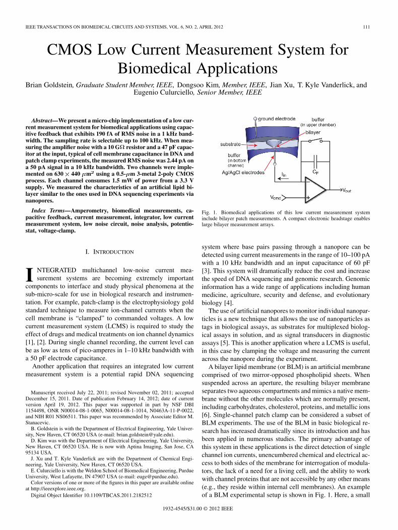
Fig. 2. System block diagram for the fabricated LCMS, featuring a current in-tegrator for the first stage, followed by an inverting post amplifier stage. The op-erational transconductance amplifier (OTA) in the first stage performs voltage-clamping to the commanded voltage, � , with respect to the experimentalground, and the input current is converted to an output voltage. The feedbackcapacitance of the integrator, � , is selectable as either 100 fF or 1 pF. Thepost amplifier can supply a voltage gain of� �� , or be bypassed based on therange of the measured input current. In our system � � ��, resulting in a gainof 10. The low-pass filter is used to filter out high frequency noise that is higherthan the selected sampling frequency.
This work is the foundation for an integrated system capableof recording whole cell experiments and also single channelexperiments. This work presents a low-noise integrated lowcurrent measurement system that features high bandwidth,sensitivity, and dynamic range to measure bidirectional cur-rents in the range required for biomedical recording whileallowing control of the voltage at the input node, known asvoltage clamping and can be scaled up for use in an integratedmultichannel system. We present a theoretical model for themeasurement noise and our fabricated system shows goodmatching. Further, we demonstrate the system’s usefulness byperforming a measurement to characterize a lipid bilayer withresults consistent with the literature.
II. SYSTEM OVERVIEW
A. Architecture
The system, shown in Fig. 2, features a current integrator forthe first stage with controllable gain, followed by an invertingpost amplifier stage. The feedback capacitance of the integratoris selectable as either 100 fF or 1 pF and the post amplifier cansupply a further gain of 10 or be bypassed based on the rangeof the measured input current. The low-pass filter is used tofilter out high frequency noise that is higher than the selectedsampling frequency. Finally, the signal passes through an outputbuffer that is capable of driving the output pad loaded by anexternal ADC. This system’s basic design has been presentedin [24].
In this system, an amplifier with capacitive feedback is usedto fix the applied voltage to the cell under test. Either resistive orcapacitive feedback could have been chosen, each with its ownadvantages and disadvantages. A resistive feedback system en-ables continuous time recording, while our capacitive feedbacksystem is a discrete time system because it requires resettingthe capacitor to avoid the amplifier reaching saturation. Capac-itive feedback was chosen because a resistive feedback systemwould add thermal noise due to the resistor. In order to reducethe thermal noise of the resistor, a very large value resistor would
GOLDSTEIN et al.: CMOS LOW CURRENT MEASUREMENT SYSTEM FOR BIOMEDICAL APPLICATIONS 113
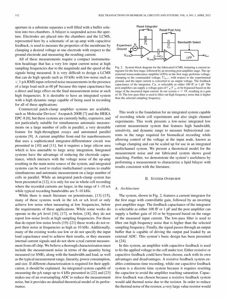
Fig. 3. Transistor schematic of the OTA used in the integrator. The specifica-tions of the OTA are summarized in Table I.
be necessary which would have too much distributed capaci-tance when implemented in this 0.5- m bulk CMOS technology[25]. The capacitive feedback system adds noise only due to theswitching effect on the capacitor. The overall noise of the mea-surement with this system will depend on the equivalent inputcircuit and the sampling frequency, and has previously been an-alyzed in [26].
The current integrator consists of an OTA with a cascodedoutput stage and is shown in Fig. 3. The cascoded output stageboosts the gain of the mirrored OTA. Wide input transistorsare used to reduce channel thermal noise, along with largearea to decrease flicker noise. The input capacitance due to thetransistors is much smaller than the electrode capacitance. Inthis technology, the NMOS mirror transistors exhibit higherlevels of flicker noise than the PMOS, so the lengths of thesewere also increased. While a PMOS input pair could havebeen chosen for the lower flicker noise properties of PMOStransistors, their lower transconductance would have requiredmore area and more power consumption to achieve the sameoverall noise level as choosing an NMOS input pair in thistechnology with this topology, so an NMOS input pair waschosen. The OTA tail transistor was biased for a current of233 A, while the current in the left and right branches isreduced by half, the ratio of the current mirror. This current waschosen to keep the overall power consumption reasonable fora mult-channel system while providing a high gain, low-noise,and enough driving current for the large capacitive load on theoutput. In open loop configuration, the DC gain is 90 dB whichwill ensure high linearity and reduce the clamping voltageoffset between the channels. The integrator is periodicallyreset, so the OTA was designed to have a phase margin of 60degrees when in a buffer configuration. The reset time of theintegrator depends on the OTA bandwidth, which decreaseswith the load capacitance. With a high 60 pF load at the inputfrom the electrode, which is also seen at the output during thereset, the GBP is 3 MHz and the minimum reset time is 2 s.In this system, the integrator is the dominant noise source andwas designed to have 5.850 nV/ of input-referred noise at10 kHz and 4.715 nV/ at 100 kHz to compromise between
TABLE ISUMMARY OF THE DESIGNED OTA AND INTEGRATOR
power, noise, and area. The OTA has an output swing greaterthan 1.5 V. The common mode input range is 1 V, allowing fora wide range of command voltages to be applied. Typically only100–500 mV are applied in patch-clamping. The integrator andits OTA were designed and simulated to have performance assummarized in Table I. The OTA was designed to achieve thesespecifications including its input referred noise, , using themethods in [27] and [28].
The integrator has two phases: reset and integration. Duringthe reset phase, the switch between the negative input terminalof the OTA and its output is closed, shorting the feedback ca-pacitor and setting the output voltage to . In this phase, theonly noise source is the op-amp. During the integration phase,the switch is opened, the feedback capacitor has an initial chargeof zero and integrates the input current. The resulting outputvoltage, of this stage ideally is
(1)
where is the chosen integration capacitor, 100 fF or 1 pF,is the integration time, and is the input current to mea-
sure.The op-amp offset and switching effects due to clock feed
through and charge injection are eliminated off-chip by corre-lated double sampling (CDS). The CDS function reduces theeffect of the low frequency noise by the subtraction operation.Since thermal noise is not correlated, the thermal noise is dou-bled, which is the reason for designing the OTA to exhibit lowthermal noise.
Since the integration time is dictated by the sampling fre-quency, and is limited by the manufacturing process limits,more gain may be required to sample the output voltage. Thepost amplifier can be enabled for this purpose. The invertingconfiguration is chosen to reduce the input common modevoltage range requirement. The gain of the post amplifier isdetermined by the ratio , where .
The low-pass filter is used to reduce the noise componentabove half of the sampling frequency and has a DC gain of 1.
The input current can be determined from the sensor’s outputvoltage by first dividing by the voltage gain of each post ampli-fying stage, , to determine the integrator’s output voltage, andthen converting this voltage to current by using the relation
(2)
114 IEEE TRANSACTIONS ON BIOMEDICAL CIRCUITS AND SYSTEMS, VOL. 6, NO. 2, APRIL 2012
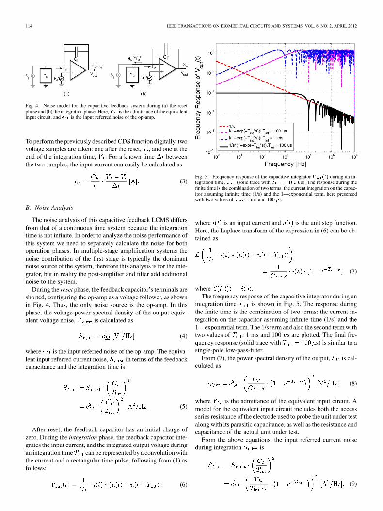
Fig. 4. Noise model for the capacitive feedback system during (a) the resetphase and (b) the integration phase. Here,� is the admittance of the equivalentinput circuit, and � is the input referred noise of the op-amp.
To perform the previously described CDS function digitally, twovoltage samples are taken: one after the reset, , and one at theend of the integration time, . For a known time betweenthe two samples, the input current can easily be calculated as
(3)
B. Noise Analysis
The noise analysis of this capacitive feedback LCMS differsfrom that of a continuous time system because the integrationtime is not infinite. In order to analyze the noise performance ofthis system we need to separately calculate the noise for bothoperation phases. In multiple-stage amplification systems thenoise contribution of the first stage is typically the dominantnoise source of the system, therefore this analysis is for the inte-grator, but in reality the post-amplifier and filter add additionalnoise to the system.
During the reset phase, the feedback capacitor’s terminals areshorted, configuring the op-amp as a voltage follower, as shownin Fig. 4. Thus, the only noise source is the op-amp. In thisphase, the voltage power spectral density of the output equiv-alent voltage noise, is calculated as
(4)
where is the input referred noise of the op-amp. The equiva-lent input referred current noise, in terms of the feedbackcapacitance and the integration time is
(5)
After reset, the feedback capacitor has an initial charge ofzero. During the integration phase, the feedback capacitor inte-grates the input current, and the integrated output voltage duringan integration time can be represented by a convolution withthe current and a rectangular time pulse, following from (1) asfollows:
(6)
Fig. 5. Frequency response of the capacitive integrator � ��� during an in-tegration time, � (solid trace with � � ����s). The response during thefinite time is the combination of two terms: the current integration on the capac-itor assuming infinite time (1/s) and the 1—exponential term, here presentedwith two values of � : 1 ms and 100 �s.
where is an input current and is the unit step function.Here, the Laplace transform of the expression in (6) can be ob-tained as
(7)
where .The frequency response of the capacitive integrator during an
integration time is shown in Fig. 5. The response duringthe finite time is the combination of two terms: the current in-tegration on the capacitor assuming infinite time (1/s) and the1—exponential term. The 1/s term and also the second term withtwo values of : 1 ms and 100 s are plotted. The final fre-quency response (solid trace with s) is similar to asingle-pole low-pass-filter.
From (7), the power spectral density of the output, is cal-culated as
(8)
where is the admittance of the equivalent input circuit. Amodel for the equivalent input circuit includes both the accessseries resistance of the electrode used to probe the unit under testalong with its parasitic capacitance, as well as the resistance andcapacitance of the actual unit under test.
From the above equations, the input referred current noiseduring integration is
(9)
GOLDSTEIN et al.: CMOS LOW CURRENT MEASUREMENT SYSTEM FOR BIOMEDICAL APPLICATIONS 115
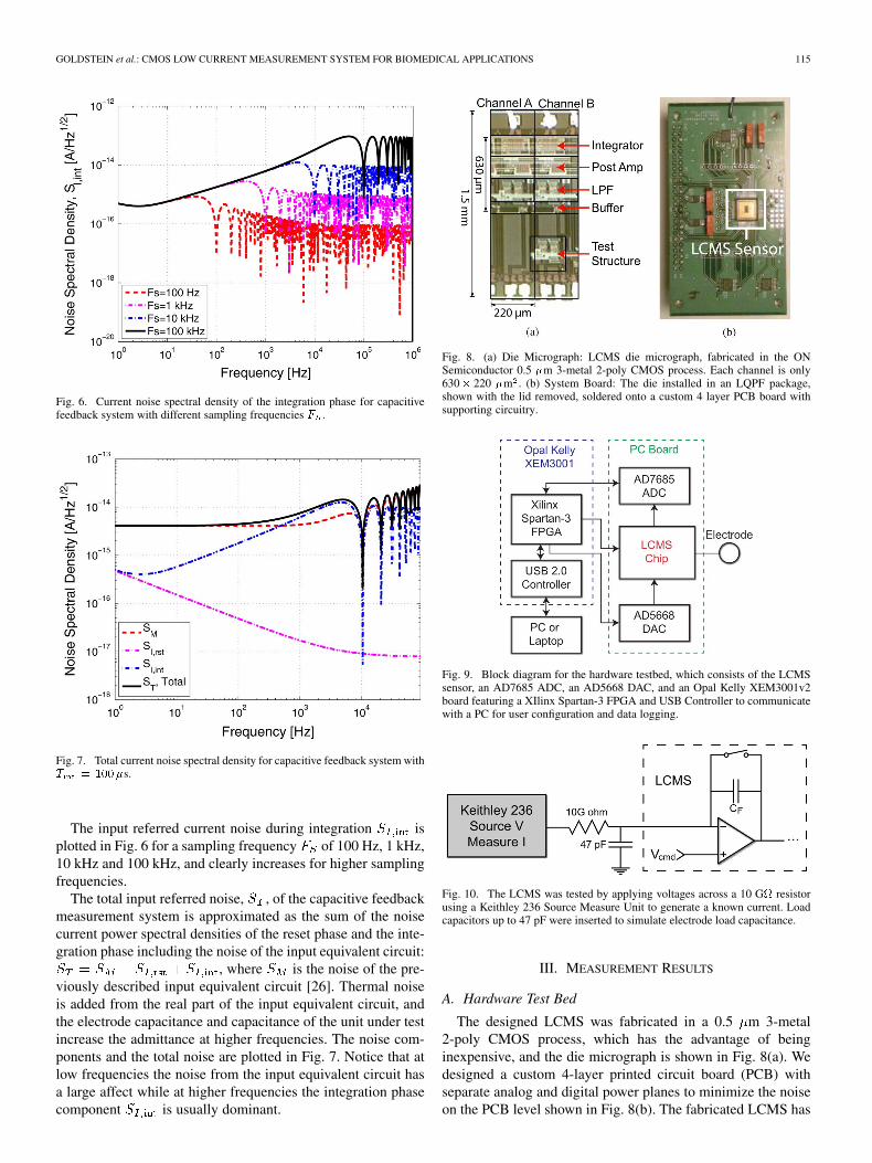
Fig. 6. Current noise spectral density of the integration phase for capacitivefeedback system with different sampling frequencies � .
Fig. 7. Total current noise spectral density for capacitive feedback system with� � ����s.
The input referred current noise during integration isplotted in Fig. 6 for a sampling frequency of 100 Hz, 1 kHz,10 kHz and 100 kHz, and clearly increases for higher samplingfrequencies.
The total input referred noise, , of the capacitive feedbackmeasurement system is approximated as the sum of the noisecurrent power spectral densities of the reset phase and the inte-gration phase including the noise of the input equivalent circuit:
, where is the noise of the pre-viously described input equivalent circuit [26]. Thermal noiseis added from the real part of the input equivalent circuit, andthe electrode capacitance and capacitance of the unit under testincrease the admittance at higher frequencies. The noise com-ponents and the total noise are plotted in Fig. 7. Notice that atlow frequencies the noise from the input equivalent circuit hasa large affect while at higher frequencies the integration phasecomponent is usually dominant.
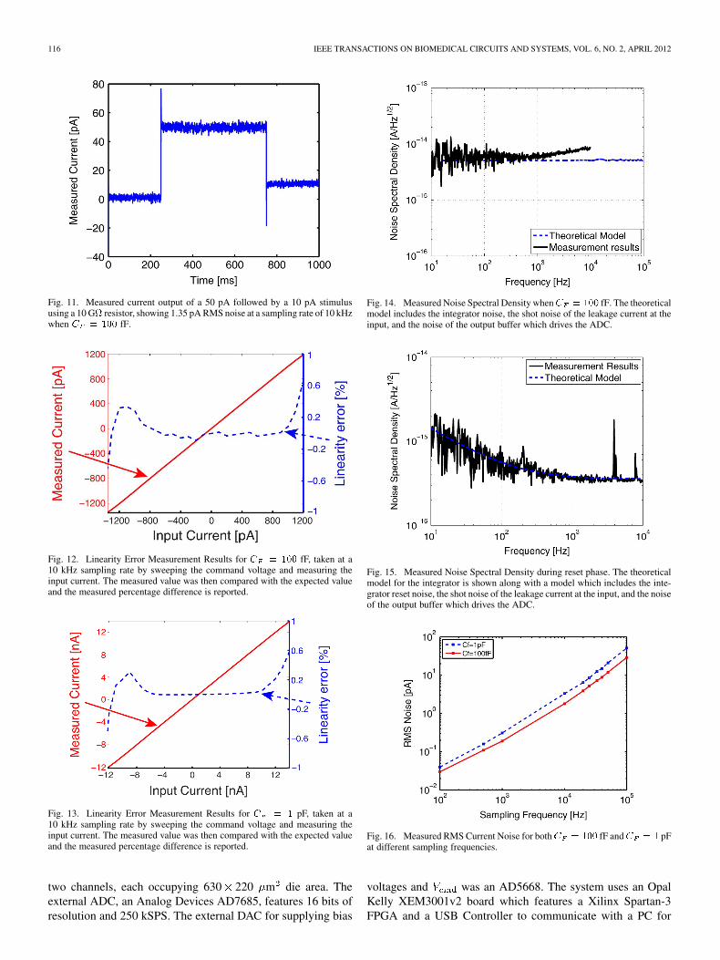
Fig. 8. (a) Die Micrograph: LCMS die micrograph, fabricated in the ONSemiconductor 0.5 �m 3-metal 2-poly CMOS process. Each channel is only630� 220 �m . (b) System Board: The die installed in an LQPF package,shown with the lid removed, soldered onto a custom 4 layer PCB board withsupporting circuitry.
Fig. 9. Block diagram for the hardware testbed, which consists of the LCMSsensor, an AD7685 ADC, an AD5668 DAC, and an Opal Kelly XEM3001v2board featuring a XIlinx Spartan-3 FPGA and USB Controller to communicatewith a PC for user configuration and data logging.
Fig. 10. The LCMS was tested by applying voltages across a 10 G� resistorusing a Keithley 236 Source Measure Unit to generate a known current. Loadcapacitors up to 47 pF were inserted to simulate electrode load capacitance.
III. MEASUREMENT RESULTS
A. Hardware Test Bed
The designed LCMS was fabricated in a 0.5 m 3-metal2-poly CMOS process, which has the advantage of beinginexpensive, and the die micrograph is shown in Fig. 8(a). Wedesigned a custom 4-layer printed circuit board (PCB) withseparate analog and digital power planes to minimize the noiseon the PCB level shown in Fig. 8(b). The fabricated LCMS has
116 IEEE TRANSACTIONS ON BIOMEDICAL CIRCUITS AND SYSTEMS, VOL. 6, NO. 2, APRIL 2012
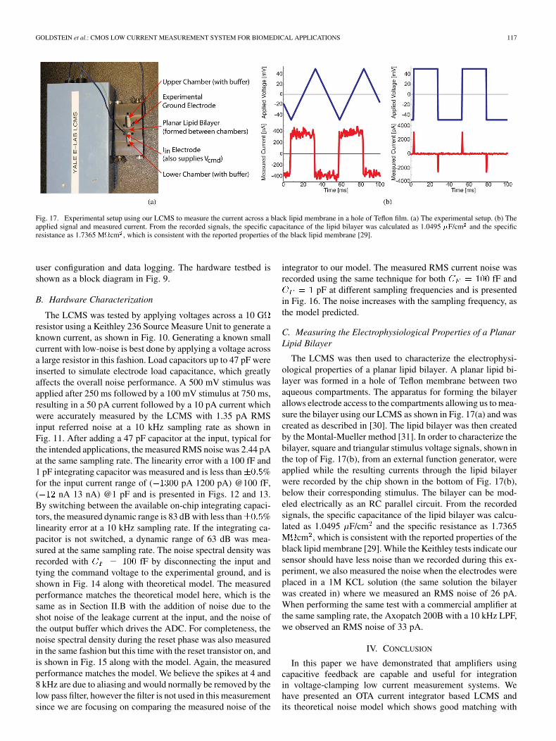
Fig. 11. Measured current output of a 50 pA followed by a 10 pA stimulususing a 10 G� resistor, showing 1.35 pA RMS noise at a sampling rate of 10 kHzwhen � � ��� fF.
Fig. 12. Linearity Error Measurement Results for � � ��� fF, taken at a10 kHz sampling rate by sweeping the command voltage and measuring theinput current. The measured value was then compared with the expected valueand the measured percentage difference is reported.
Fig. 13. Linearity Error Measurement Results for � � � pF, taken at a10 kHz sampling rate by sweeping the command voltage and measuring theinput current. The measured value was then compared with the expected valueand the measured percentage difference is reported.
two channels, each occupying 630 220 m die area. Theexternal ADC, an Analog Devices AD7685, features 16 bits ofresolution and 250 kSPS. The external DAC for supplying bias
Fig. 14. Measured Noise Spectral Density when� � ��� fF. The theoreticalmodel includes the integrator noise, the shot noise of the leakage current at theinput, and the noise of the output buffer which drives the ADC.
Fig. 15. Measured Noise Spectral Density during reset phase. The theoreticalmodel for the integrator is shown along with a model which includes the inte-grator reset noise, the shot noise of the leakage current at the input, and the noiseof the output buffer which drives the ADC.
Fig. 16. Measured RMS Current Noise for both� � ��� fF and� � � pFat different sampling frequencies.
voltages and was an AD5668. The system uses an OpalKelly XEM3001v2 board which features a Xilinx Spartan-3FPGA and a USB Controller to communicate with a PC for
GOLDSTEIN et al.: CMOS LOW CURRENT MEASUREMENT SYSTEM FOR BIOMEDICAL APPLICATIONS 117
Fig. 17. Experimental setup using our LCMS to measure the current across a black lipid membrane in a hole of Teflon film. (a) The experimental setup. (b) Theapplied signal and measured current. From the recorded signals, the specific capacitance of the lipid bilayer was calculated as 1.0495 �F/cm and the specificresistance as 1.7365 M�cm , which is consistent with the reported properties of the black lipid membrane [29].
user configuration and data logging. The hardware testbed isshown as a block diagram in Fig. 9.
B. Hardware Characterization
The LCMS was tested by applying voltages across a 10 Gresistor using a Keithley 236 Source Measure Unit to generate aknown current, as shown in Fig. 10. Generating a known smallcurrent with low-noise is best done by applying a voltage acrossa large resistor in this fashion. Load capacitors up to 47 pF wereinserted to simulate electrode load capacitance, which greatlyaffects the overall noise performance. A 500 mV stimulus wasapplied after 250 ms followed by a 100 mV stimulus at 750 ms,resulting in a 50 pA current followed by a 10 pA current whichwere accurately measured by the LCMS with 1.35 pA RMSinput referred noise at a 10 kHz sampling rate as shown inFig. 11. After adding a 47 pF capacitor at the input, typical forthe intended applications, the measured RMS noise was 2.44 pAat the same sampling rate. The linearity error with a 100 fF and1 pF integrating capacitor was measured and is less than %for the input current range of ( pA 1200 pA) @100 fF,( nA 13 nA) @1 pF and is presented in Figs. 12 and 13.By switching between the available on-chip integrating capaci-tors, the measured dynamic range is 83 dB with less than %linearity error at a 10 kHz sampling rate. If the integrating ca-pacitor is not switched, a dynamic range of 63 dB was mea-sured at the same sampling rate. The noise spectral density wasrecorded with fF by disconnecting the input andtying the command voltage to the experimental ground, and isshown in Fig. 14 along with theoretical model. The measuredperformance matches the theoretical model here, which is thesame as in Section II.B with the addition of noise due to theshot noise of the leakage current at the input, and the noise ofthe output buffer which drives the ADC. For completeness, thenoise spectral density during the reset phase was also measuredin the same fashion but this time with the reset transistor on, andis shown in Fig. 15 along with the model. Again, the measuredperformance matches the model. We believe the spikes at 4 and8 kHz are due to aliasing and would normally be removed by thelow pass filter, however the filter is not used in this measurementsince we are focusing on comparing the measured noise of the
integrator to our model. The measured RMS current noise wasrecorded using the same technique for both fF and
pF at different sampling frequencies and is presentedin Fig. 16. The noise increases with the sampling frequency, asthe model predicted.
C. Measuring the Electrophysiological Properties of a PlanarLipid Bilayer
The LCMS was then used to characterize the electrophysi-ological properties of a planar lipid bilayer. A planar lipid bi-layer was formed in a hole of Teflon membrane between twoaqueous compartments. The apparatus for forming the bilayerallows electrode access to the compartments allowing us to mea-sure the bilayer using our LCMS as shown in Fig. 17(a) and wascreated as described in [30]. The lipid bilayer was then createdby the Montal-Mueller method [31]. In order to characterize thebilayer, square and triangular stimulus voltage signals, shown inthe top of Fig. 17(b), from an external function generator, wereapplied while the resulting currents through the lipid bilayerwere recorded by the chip shown in the bottom of Fig. 17(b),below their corresponding stimulus. The bilayer can be mod-eled electrically as an RC parallel circuit. From the recordedsignals, the specific capacitance of the lipid bilayer was calcu-lated as 1.0495 F/cm and the specific resistance as 1.7365M cm , which is consistent with the reported properties of theblack lipid membrane [29]. While the Keithley tests indicate oursensor should have less noise than we recorded during this ex-periment, we also measured the noise when the electrodes wereplaced in a 1M KCL solution (the same solution the bilayerwas created in) where we measured an RMS noise of 26 pA.When performing the same test with a commercial amplifier atthe same sampling rate, the Axopatch 200B with a 10 kHz LPF,we observed an RMS noise of 33 pA.
IV. CONCLUSION
In this paper we have demonstrated that amplifiers usingcapacitive feedback are capable and useful for integrationin voltage-clamping low current measurement systems. Wehave presented an OTA current integrator based LCMS andits theoretical noise model which shows good matching with
118 IEEE TRANSACTIONS ON BIOMEDICAL CIRCUITS AND SYSTEMS, VOL. 6, NO. 2, APRIL 2012
our fabricated system. We have measured the performanceof the system and demonstrated its usefulness in biomedicalapplications by using it to characterize a lipid bilayer. Themeasurement noise depends on the noise of the equivalentinput circuit, the noise of the op-amp, the size of the integra-tion capacitor, and the integration time. We believe capacitivefeedback to be capable of very low levels of noise and to havesuperior noise performance compared to resistive feedbacksystems that are usually dominated by the thermal of noise oftheir feedback resistor.
Because high frequency noise is the dominant componentof the overall RMS current noise, especially when high sam-pling frequencies are desired, we recommend using an ampli-fier with very low thermal noise levels. The amplifier must alsohave enough common mode range to cover the clamping voltagerange, enough output swing to avoid saturation within the inte-gration time for the given integration capacitor and input cur-rent, and high linearity, such as in the system presented in thiswork. CDS can be used to reduce flicker noise. Because anynoise on the command voltage adds to the clamping voltage andtherefore output noise, we recommend having a very clean com-mand voltage or add an input low pass filter on the chip to filterout noise on the stimulus. Because the input equivalent circuitalso contributes noise, especially at lower frequencies, we ad-vise users to minimize parasitic input capacitance. Additionally,leakage current can contribute shot noise to the input and shouldbe minimized. We also advise users to minimize external envi-ronmental noise sources by working in a faraday cage.
ACKNOWLEDGMENT
The authors would like to thank B. Martini for his program-ming assistance.
REFERENCES
[1] O. Hamill, A. Marty, E. Neher, B. Sakmann, and F. Sigworth, “Im-proved patch-clamp techniques for high-resolution current recordingfrom cells and cell-free membrane patches,” Pflugers Arch. Eur. J.Phys., vol. 391, no. 2, pp. 85–100, 1981.
[2] F. Sigworth and K. Klemic, “Microchip technology in ion-channel re-search,” IEEE Trans. Nanobiosci., vol. 4, pp. 121–127, 2005.
[3] J. Clarke, H. Wu, L. Jayasinghe, A. Patel, S. Reid, and H. Bayley,“Continuous base identification for single-molecule nanopore DNA se-quencing,” Nature Nanotechnol., vol. 4, pp. 265–270, 2009, 4.
[4] D. Branton et al., “The potential and challenges of nanopore se-quencing,” Nature Biotechnol., vol. 26, pp. 1146–1153, 2008.
[5] S. G. Penn, L. He, and M. J. Natan, “Nanoparticles for bioanalysis,”Current Opin. Chem. Biol., vol. 7, pp. 609–615, Oct. 2003.
[6] H. T. Tien and A. L. Ottova, “The lipid bilayer concept and its exper-imental realization: From soap bubbles, kitchen sink, to bilayer lipidmembranes,” J. Membr. Sci., vol. 189, no. 1, pp. 83–117, 2001.
[7] Axon Instruments [Online]. Available: http://www.axon.com[8] HEKA Electronics [Online]. Available: http://www.heka.com[9] C. Wood and C. Williams, “Patch-clamping by numbers,” Drug Disc.
Today, vol. 4, pp. 434–441, 2004.[10] G. Ferrari, F. Gozzini, and M. Sampietro, “A current-sensitive
front-end amplifier for nano-biosensors with a 2 MHz BW,” in Proc.IEEE Int. Solid-State Circuits Conf., Dig. Tech. Papers, 2007, pp.164–165.
[11] G. Ferrari, F. Gozzini, A. Molari, and M. Sampietro, “Transimpedanceamplifier for high sensitivity current measurements on nanodevices,”IEEE J. Solid-State Circuits, vol. 44, no. 5, pp. 1609–1616, May 2009.
[12] P. Weerakoon, K. Klemic, F. Sigworth, and E. Culurciello, “An inte-grated patch-clamp potentiostat with electrode compensation,” IEEETrans. Biomed. Circuits Syst., vol. 3, pp. 117–125, 2009.
[13] R. Genov, M. Stanacevic, M. Naware, G. Cauwenberghs, and N.Thakor, “16-channel integrated potentiostat for distributed neuro-chemical sensing,” IEEE Trans. Circuits Syst. I, Reg. Papers, vol. 53,no. 11, pp. 2371–2376, Nov. 2006.
[14] M. Ahmadi and G. Jullien, “Current-mirror-based potentiostats forthree-electrode amperometric electrochemical sensors,” IEEE Trans.Circuits Syst. I, Reg. Papers, vol. 56, no. 7, pp. 1339–1348, July 2009.
[15] S. Hwang and S. Sonkusale, “CMOS VLSI potentiostat for portableenvironmental sensing applications,” IEEE Sensors J., vol. 10, no. 4,pp. 820–821, Apr. 2010.
[16] M. Breten, T. Lehmann, and E. Braun, “Integrating data converters forpicoampere currents from electrochemical transducers,” in Proc. IEEEInt. Symp. Circuits and Systems, Geneva, Switzerland, 2000, vol. 5, pp.709–712.
[17] H. Narula and J. Harris, “A time-based VLSI potentiostat for ion cur-rent measurements,” IEEE Sensors J., vol. 6, no. 2, pp. 239–247, Apr.2006.
[18] A. Gore, S. Chakrabartty, S. Pal, and E. Alocilja, “A multichannelfemtoampere-sensitivity potentiostat array for biosensing applica-tions,” IEEE Trans. Circuits Syst. I, Reg. Papers, vol. 53, no. 11, pp.2357–2363, Nov. 2006.
[19] S. Ayers, K. Gillis, M. Lindau, and B. Minch, “Design of a CMOSpotentiostat circuit for electrochemical detector arrays,” IEEE Trans.Circuits Syst. I, Reg. Papers, vol. 54, no. 4, pp. 736–744, Apr. 2007.
[20] M. Stanacevic, K. Murari, A. Rege, G. Cauwenberghs, and N. Thakor,“Vlsi potentiostat array with oversampling gain modulation for wide-range neurotransmitter sensing,” IEEE Trans. Biomed. Circuits Syst.,vol. 1, no. 1, pp. 63–72, Mar. 2007.
[21] C. Yang, Y. Huang, B. Hassler, R. Worden, and A. Mason, “Am-perometric electrochemical microsystem for a miniaturized proteinbiosensor array,” IEEE Trans. Biomed. Circuits Syst., vol. 3, no. 3, pp.160–168, June 2009.
[22] M. Bennati, F. Thei, M. Rossi, M. Crescentini, G. D’Avino, A. Baschi-rotto, and M. Tartagni, “A sub-pa delta-sigma current amplifier forsingle-molecule nanosensors,” in Proc. IEEE Int. Solid-State CircuitsConf., Dig. Tech. Papers, Feb. 2009, pp. 348–349, 349a.
[23] F. Thei, M. Rossi, M. Bennati, M. Crescentini, F. Lodesani, H. Morgan,and M. Tartagni, “Parallel recording of single ion channels: A hetero-geneous system approach,” IEEE Trans. Nanotechnol., vol. 9, no. 3, pp.295–302, May 2010.
[24] B. Goldstein, D. Kim, A. Rottigni, J. Xu, T. K. Vanderlick, and E.Culurciello, “CMOS low current measurement system for biomedicalapplications,” in Proc. IEEE Int. Symp. Circuits Syst., Rio de Janeiro,Brazil, May 2011, pp. 1017–1020.
[25] P. Weerakoon, K. Klemic, F. Sigworth, and E. Culurciello, “A low-noise miniaturized patch-clamp amplifier,” in Proc. IEEE LISA Conf.,NIH, Nov. 8th, 2007.
[26] D. Kim, W. Tang, B. Goldstein, P. Weerakoon, and E. Culurciello,“Performance comparison of low current measurement systems forbiomedical applications,” in Proc. IEEE Int. Symp. Circuits andSystems, Paris, France, May 2010.
[27] R. J. Baker, “Institute of Electrical and Electronics Engineers and IEEESolid-State Circuits Society,” in CMOS: Circuit Design, Layout andSimulation, ser. IEEE Press Series on Microelectronic Systems. Pis-cataway, NJ: IEEE Press, 2008.
[28] B. Razavi, Design of Analog CMOS Integrated Circuits, ser. McGraw-Hill series in electrical and computer engineering. New York: Mc-Graw-Hill, 2001.
[29] F. Yi, J. Xu, A. M. Smith, A. N. Parikh, and D. A. LaVa,“Nanofiber-supported phospholipid bilayers,” Soft Matter, vol. 5,no. 24, pp. 5037–5041, 2009.
[30] D. P. Nikolelis and U. J. Krull, “Bilayer lipid membranes for electro-chemical sensing,” Electroanal., vol. 5, pp. 539–545, 1993.
[31] M. Montal and P. Mueller, “Formation of bimolecular membranes fromlipid monolayers and a study of their electrical properties,” Proc. Nat.Acad. Sci. USA, vol. 69, no. 12, pp. 3561–3566, 1972.
Brian Goldstein (GS’08) received the B.S. degreein computer and systems engineering and computerscience from Rensselaer Polytechnic Institute, Troy,NY, in 2006, and the M.S. and M.Phil. degrees inelectrical engineering from Yale University, NewHaven, CT, in 2010 and 2011, respectively.
Currently, he is working toward the Ph.D. degreeat Yale University. From 2006 to 2008, he workedon embedded systems at Goodrich Pump and EngineControl Systems, N.A., West Hartford, CT. His re-search interests include analog and mixed-signal in-
tegrated circuits, low-noise circuit design, and systems engineering for biomed-ical applications.
GOLDSTEIN et al.: CMOS LOW CURRENT MEASUREMENT SYSTEM FOR BIOMEDICAL APPLICATIONS 119
Dongsoo Kim (M’02) received the M.S. and Ph.D.degrees in electrical and electronics engineering fromYonsei University, Seoul, Korea, in 2004 and 2008,respectively.
Currently, he works as a Senior Analog DesignEngineer at Aptina Imaging, San Jose, CA. From2008 to 2010, he was a Postdoctoral Associate in theDepartment of Electrical Engineering, Yale Univer-sity, New Haven, CT. His research interests includeCMOS image sensors, smart sensors, low-noisecircuit design, and biomedical instrumentation.
Jian Xu received the Ph.D. degree in electrical en-gineering from Yale University, New Haven, CT in2008.
Currently, he is a Postdoctoral Associate inthe Department of Chemical Engineering at YaleUniversity. His research interests include under-standing and exploiting the function of natural cells,including cell signaling and energy conversion, bycreating synthetic versions of the natural cells. Theseartificial cells are fabricated by various engineeringapproaches, including electroformation of GUVs,
droplet based bilayer, soft lithography, and planar lipid bilayer formation fromair-water interfaces.
T. Kyle Vanderlick received the B.S. and M.S. de-grees in chemical engineering from Rensselaer Poly-technic Institute, Troy, NY, in 1981 and 1983, respec-tively, and the Ph.D. degree from the University ofMinnesota, Twin Cities, Minneapolis and St. Paul, in1988.
She is the Dean of the School of Engineering andApplied Science and the Thomas E. Golden, Jr. Pro-fessor of Engineering at Yale University, New Haven,CT. Noted for her research in interfacial phenomena,currently centered on biological and synthetic mem-
brane-based materials, she received the Presidential Young Investigator Awardin 1989 as well as the prestigious David and Lucile Packard Fellowship in 1991.She is also the recipient of numerous teaching awards including the highest suchhonors at the University of Pennsylvania, Philadelphia (1993 Christian R. andMary F. Lindback Award for Distinguished Teaching) and Princeton Univer-sity, Princeton, NJ (2002 President’s Award for Distinguished Teaching). AsDean of Engineering, she led the establishment of the new Yale School of En-gineering and Applied Science, and is directing new initiatives in both teachingand research to shape the school’s distinctive identity and its premier role inengineering education.
Eugenio Culurciello (S’97-M’99–SM’11) receivedthe Ph.D. degree in electrical and computer en-gineering from The Johns Hopkins University,Baltimore, MD, in 2004.
He is an Associate Professor in the Weldon Schoolof Biomedical Engineering, Purdue University, WestLafayette, IN, where he directs the ‘e-Lab’ labora-tory. His research interests include analog and mixed-mode integrated circuits for biomedical instrumenta-tion, synthetic vision, bio-inspired sensory systemsand networks, biological sensors, and silicon-on-in-
sulator design. He was the recipient of The Presidential Early Career Awardfor Scientists and Engineers (PECASE) and Young Investigator Program fromONR, the Distinguished Lecturer of the IEEE (CASS), and is the author of Sil-icon-on-Sapphire Circuits and Systems, Sensor and Biosensor Interfaces (Mc-Graw-Hill: New York) in 2009.