Embed Size (px)
Citation preview

International Journal of Computer and Electrical Engineering, Vol.2, No.6, December, 2010 1793-8163
1010
Abstract—A resource efficient with low computational
overheads SVPWM algorithm for three phase voltage source inverter which is used to supply variable voltage and variable frequency to three phase AC drives is proposed in this paper. Because of its advantages like lower switching losses, higher dc-bus utilization SVPWM scheme becomes the preferred PWM technique for various three-phase power converter applications. Conventional SVPWM algorithm involves complex mathematics and requires more hardware resources to implement and takes more time for its execution. The Field Programmable Gate Arrays (FPGAs) offer high computational ability and flexibility due to their parallel execution and reconfigurable hardware. Hence the scheme suggests the implementation of a resource efficient algorithm with low computational overheads for SVPWM generation using FPGA and obtains higher sampling rates with minimal use of hardware resources. Resource utilization of proposed algorithm obtained is 4% for XILINX XC3S500E processor operating at 50 MHz. The output fundamental frequency can be adjusted from 0.1Hz to 1500Hz and PWM switching frequency can be set from 200 to 50 KHz. The adjustable delay time logic for PWM gating signals is also implemented. The proposed algorithm is tested for 3-phase induction motor with VSI and the experimented results are validated.
Index Terms—Digital Control, FPGA, SVPWM, Xilinx
XC3S500E
I. INTRODUCTION Variable voltage and frequency supply for ac drive is
invariably obtained from three-phase Voltage Source Inverter. A number of PWM techniques have been presented to obtain variable voltage and variable frequency supply[4]. Space Vector Pulsewidth Modulation has become one of the most important PWM method for three-phase voltage source inverters[5]. It has an advantages over carrier-based sine tringle pwm such as higher dc bus utilization, lower switching losses and less harmonic distortions [14].
In order to implement SVPWM algorithm DSPs are widely used but the execution of SVPWM algorithm in less number of machine cycles is need of many applications which can not be satisfied with conventioanl DSPs because
Manuscript received June 30, 2010. D. N. Sonawane is with the Department of Instrumentation and Control
of College of Engineering, Pune-411005, MH,INDIA (91-020- 25507185; fax: 91-020-25507299; e-mail: dns.instru@ coep.ac.in).
M. S. Sutaone is with Department of Electronics and Communication of College of Engineering, Pune-411005, MH, INDIA (91-020- 25507141; fax: 91-020-25507299; e-mail: mssutaone@ extc.coep.org.in)
B. N. Choudhari is with Department of Electrical Engineering of College of Engineering, Pune-411005, MH, INDIA (91-020- 25507112; fax: 91-020-25507299; e-mail: bnc.elec@ coep.ac.in)
they executes instructions sequentially and thus requires more time to compute. Whereas, field programmable gate array (FPGA) performs the entire procedures with concurrent operation by using its reconfigurable hardware and parallel processing. Employing FPGA to realize PWM strategies provides advantages such as rapid prototyping, simple hardware and software design, higher switching frequency and reduction of computational overheads [5]. Computational Complexity and resource utiliazation of conventional SVPWM algorithm increases thus the execution time with number of levels of converter [2].
In this paper, a resource efficient SVPWM algorithm is proposed which reduces computational overheads and solves the problem of high sampling time in real time applications. The proposed algorithm uses only adders, subtractors, comparators, shifters,etc to be implemeted using FPGA’s and takes less number of resources and execution time than conventional algorithm. Finally, experimental results from an inverter prototype are presented to confirm the validity and performance of the designed SVPWM algorithm. Fig.1 shows the open loop control scheme for three phase induction motor which is used for testing and validation of algorithm.
This paper is organized as follows. Section II introduces conventional SVPWM algorithm and mathematics involved in it. Section III discusses simplified SVPWM algorithm. Section IV describes FPGA implementation of proposed simplified SVPWM algorithm and experimental results. Finally conclusion is in Section V.
Fig. 1 Open loop scheme for three-phase induction motor
II. CONVENTIONAL SVPWM ALGORITHM
To implement the space vector PWM, the voltage equations in the abc reference frame can be transformed into
FPGA Implementation of Simplified SVPWM Algorithm for Three Phase Voltage Source
Inverter D. N. Sonawane, M. S. Sutaone , B. N. Choudhari and Abhijeet Badurkar
International Journal of Computer and Electrical Engineering, Vol.2, No.6, December, 2010 1793-8163
1011
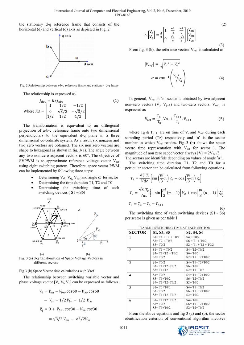
the stationary d-q reference frame that consists of the horizontal (d) and vertical (q) axis as depicted in Fig. 2
Fig. 2 Relationship between a-b-c reference frame and stationay d-q frame
The relationship is expressed as 1
Where 1 1/2 1/20 √3 2⁄ √3 2⁄1/2 1/2 1/2
The transformation is equivalent to an orthogonal projection of a-b-c reference frame onto two dimensional perpendiculars to the equivalent d-q plane in a three dimensional co-ordinate system. As a result six nonzero and two zero vectors are obtained. The six non zero vectors are shape to hexagonal as shown in fig. 3(a). The angle between any two non zero adjacent vectors is 60°. The objective of SVPWM is to approximate reference voltage vector Vref using eight switching pattern. Therefore, space vector PWM can be implemented by following three steps:
• Determining Vd, Vq, Vref and angle α for sector • Determining the time duration T1, T2 and T0 • Determining the switching time of each
switching devices ( S1 ~ S6)
(a) (b) Fig. 3 (a) d-q transfomation of Space Voltage Vectors in different sectors Fig 3 (b) Space Vector time calculations with Vref
The relationship between switching variable vector and phase voltage vector [Va Vb Vc] can be expressed as follows. . 60 . 60
1 2⁄ 1 2⁄
0 . 30 . 30
√3 2 √3 2
(2)
VV 1 0 √ √ VVV
(3) From fig. 3 (b), the reference vectror Vref is calculated as
(4)
In general, Vref in ‘n’ sector is obtained by two adjecent non-zero vectors (Vj, Vj+1) and two-zero vectors. Vref is expressed as V T T . Vn TT . V 5
where Tn & Tn+1 are on time of Vn and Vn+1 during each sampling period (Tz) respectively and ‘n’ is the sector number in which Vref resides. Fig 3 (b) shows the space vectro time representation with Vref for sector 1. The magnitude of non zero sapce vector always ||Vj||= 2Vdc /3. The sectors are identifide depending on values of angle ’.
The switching time duration T1, T2 and T0 for a perticular sector can be calculated from following equations . √3. sin 3 cos 3
√3. sin 3 1 cos 3 1 (6)
The switching time of each switching devices (S1~ S6) per sector is given as per table I
TABLE I SWITCHING TIME AT EACH SECTOR
SECTOR S1, S3, S5 S2, S4, S6 1 S1= T1 + T2 + T0/2
S3= T2 + T0/2 S5= T0/2
S4 = T0/2 S6 = T1 + T0/2 S2 = T1 + T2 + T0/2
2 S1= T1 + T0/2 S3= T1+T2 + T0/2 S5= T0/2
S4= T2+T0/2 S6= T0/2 S2= T1+T2+T0/2
3 S1= T0/2 S3= T1+T2+T0/2 S5= T1+T2
S4= T1+T2+T0/2 S6= T0/2 S2= T1+T0/2
4 S1= T0/2 S3= T1+T0/2 S5= T1+T2+T0/2
S4= T1+T2+T0/2 S6= T2+T0/2 S2= T0/2
5 S1= T2+T0/2 S3= T0/2 S5= T1+T2+T0/2
S4= T1+T0/2 S6= T1+T2+T0/2 S2= T0/2
6 S1= T1+T2+T0/2 S3= T0/2 S5= T1+T0/2
S4= T0/2 S6= T1+T2+T0/2 S2= T2+T0/2
From the above equations and fig 3 (a) and (b), the sector identification criterion of conventional algorithm involves
International Journal of Computer and Electrical Engineering, Vol.2, No.6, December, 2010 1793-8163
1012
floating point operations as to get angle that requires calculating inverse tan function. Because of sine function and square root values involved in computation switching time duration i.e. T1, T2 and T0, implementation of conventional algorithm using digital processor becomes difficult. In context with FPGA implementation the floating point operations and trigonometric functions increases resource utilization thus execution time. Attempt to be made to simplify mathematical equations which require only addition, subtraction, shifting, etc. to implement the SVPWM algorithm for three phase VSI.
III. SIMPLIFIED ALGORITHM
The conventional SVPWM algorithm includes d-q transformation of three input voltages Van, Vbn and Vcn as given by equation (4) this transformation requires value of √3 to be calculated it is difficult to implement floating point numbers using FPGA. Hence instead of d-q transformation, intermediate transformation vectors are used. The eq. (3) can be written as:
23 13 13 &
1√3 1√3 7 13 2 1√3
(8) By defining intermediate variables as Xd and Xq, the eq.
(7) written as: 2 & (9)
By combining eq. (8) and (9), the Vd and Vq are
expressed in terms of intermediate vectors as: √ (10)
Hence the algorithm needs only to calculate Xd and Xq which requires simple operators namely shifter (for multiplication by 2), adder and subtractor. The corresponding Vd and Vq calculated by normalizing the values with 1/3 and 1/√3 units.
The determination of sector depends only on the sign of Xd and Xq as per following rules. Determination of the sectors can be done by simply checking 3 conditions:
Condition 1: sign of Xd Condition 2: sign of Xq Condition 3: |Xd | > |Xq/2| The rules to find sectors: Rule 1: if (Xd>0 & Xq>0 & |Xd|>|Xq/2|)
Sector- 1
Rule 2: if (Xd>0 & Xq>0 & |Xd|<|Xq/2|) Sector- 2 OR if (Xd<0 & Xq>0 & |Xd|<|Xq/2|) Sector- 2
Rule 3: if (Xd<0 & Xq>0 & |Xd|>|Xq/2|) Sector-3
Rule 4: if (Xd<0 & Xq<0 & |Xd|>|Xq/2|) Sector-4
Rule 5: if (Xd>0 & Xq<0 & |Xd|<|Xq/2|) Sector-5 OR if (Xd<0 & Xq <0 & |Xd|<|Xq/2|) Sector-5
Rule 6: if (Xd>0 & Xq<0 & |Xd|>|Xq/2|) Sector-6
For a symmetric space vector PWM, the output voltage i.e.
Xd and Xq can be in any of the sector 1 to sector 6 is given by the equation
TT TPWMM XX (11)
Eq. (11) shows that every PWM period, the output
voltages are approximated as (Tz/Vdc) by switching between the two non zero basic vectors that border the sector of the current output voltages. The sum of T and T should be less than or equal toTPWM and rest of period the switching time should be T . The M is called as decomposition matrix, given as
M M MM M
Applying equation (10) to (6), the switching time can be
calculated as
2√3 sin 3 cos 32√3 sin 3 1 cos 3 1
(12)
If Vdc is normalized with √3 per unit, and Tz is set to √3 per unit, the four coefficients in eq. (12) will alter their values according to the sector ‘n’. If reference vector is located in sector I, then ‘n’=1, then M 1, M 1/2,M 0 and M 1.
The coefficients of decomposition matrix according to sector is given in Table II
TABLE II COEFFICIENTS OF DECOMPOSITION MATRIX Sector
‘n’ 1 2 3 4 5 6 M 1 1 0 -1 -1 0

International Journal of Computer and Electrical Engineering, Vol.2, No.6, December, 2010 1793-8163
1013
M -1/2 1/2 1 1/2 -1/2 -1 M 0 -1 -1 0 1 1 M 1 1/2 -1/2 -1 -1/2 1/2
So from eq. (11) the switching times are calculated as
[T ] = [M M XX [T ] =[M M XX
[T ] = √3 T + T (13)
The calculation for eq. (13) will requires simple operators such as shifters, adders and subtractors including Xd, and Xq. Thus the proposed algorithm reduces the complexity of conventional SVPWM algorithm.
IV. FPGA IMPLEMENTATION
Fig. 4 shows the internal architecture of simplified SVPWM algorithm implemented using Spartan 3 FPGA (XILINX XC3S500E)
Fig. 4 Internal Architecture of Simplified SVPWM Algorithm
The architecture mainly consists of five major blocks
1. 3-2 Transformation Module: Values of three phase voltages i.e. Va, Vb, Vc is input to
this block. This module transforms three phase voltage reference frame to two phase voltage reference frame using equations (10). To implement in FPGA the resources requires are only adders, and subtractors.
2. Sector determination module:
The input to this module is Xd and Xq values generated by three to two phase transformation module. This module checks three conditions as explained earlier and the corresponding sectors get determined as per the rules explained earlier.
Result of condition Xd>0 is stored in 1 bit variable as C1. Result of condition Xq>0 is stored in 1 bit variable as C2 And result of condition |Xd|>|Xq/2| is stored as C3. These variables are appended to form a three bit array
named as sect. The array sect = {C1, C2, C3}. The sector can be determined from the value of sect according to following table:
TABLE III VALUES OF ARRAYS ACCORDING TO SECTOR
Sector Array value
1 7
2 2,6
3 3
4 1
5 0,4
6 5
For example, if Xd>0, then C1=1 and Xq<0, C2=0 and
for |Xd|>|Xq/2|, C3=1. So sect= {1,0,1}=5. So according to table III, the sector 6 will get selected.
3. Switching time calculation module: Switching time calculation requires values of Xd, Xq and
sectors. These values are calculated by two blocks as explained earlier. The values of parameters T and T ] are determined from equation (13). The coefficients of decomposition matrix and their values are obtained from table II based on sector number.
4. Symmetrical PWM generation module: This module is the heart of this algorithm which is
responsible for generation of six symmetrical PWM signals. This module requires sector number and switching time values calculated by previous blocks. The PWM switching frequency can be adjusted in this module. Dead time generation module is a part of this module.
Figure 5(a) and 5(b) shows the waveform produced for sector I and II as a sample.
Figure 5 (a) Symmetrical PWM for sector I
Figure 5 (b) Symmetrical PWM for sector II
Each waveform has following properties 1. Each PWM channel switches twice per PWM
period except when duty cycle is 0 or 100%

International Journal of Computer and Electrical Engineering, Vol.2, No.6, December, 2010 1793-8163
1014
2. There is fixed switching order among the three PWM channels for each sector
According to figure 5 (a) and 5 (b) the values of different PWM outputs are changes only for the states S2, S3, S5, and S6 out of which the pattern of S2 and S6 are always same as well the pattern of S3 and S5 are always same, Hence 3 bit array (S2ar and S3ar) is created each for S2 (same for S6) and S3 (same for S5) respectively. Values are assigned to these arrays based on sector of Vref according to table IV.
TABLE IV SYMMETRICAL PWM OUTPUTS ACCORDING TO STATES
STATES
N 1 2 3 4 5 6
S2,S6
PWMA 1 0 0 0 0 1
PWMB 0 1 1 0 0 0
PWMC 0 0 0 1 1 0
S3,S5
PWMA 1 1 0 0 1 1
PWMB 1 1 1 1 0 0
PWMC 0 0 1 1 1 1
The value of switching time Tz is kept equal to Vdc for normalization.
A counter is set to 0 at the beginning of each switching period which counts up to Tz. The time step to this counter is adjustable. Larger time step means smaller frequency and vice versa. Thus the PWM frequency can be adjusted by adjusting the time step. For C < T0/4, PWMA, PWMB and PWMC are off. (Refer S1 state of fig.5). Then for T0/4 ≤ C < Tn’/2, the PWMA, PWMB and PWMC are assigned values of S2ar which are sector dependent (state S2 of Fig.5). For state S3, the values of PWMA, PWMB and PWMC are assigned as given by S3ar.
This procedure is continued till the counter reaches Tz. Thus PWM signals for one switching period are generated. Now the counter is set to zero and again same procedure is repeated for new values of Vref Thus symmetrical PWM signals are continuously generated. The table shows the comparison of resource utilization for conventional SVPWM and simplified SVPWM algorithm implemented using Xilinx Spartan 3 FPGA (XC3S500E) operating at 50MHz.
TABLE V COMPARISION OF SVPWM SCHEMES IMPLEMENTED
USING SPARTEN 3 FPGA OPERATING AT 50MHZ
Scheme Multipliers Dividers Adders/Subtractors
CLB’s % Utilization
Conve- -ntional
8 2 24+ 1796 15%
Proposed 0 0 32+ 490 4%
5) Dead time generation module In ideal conditions, the gating signals to the power
switches of same phase leg of the PWM inverter should be complementary. However, the turn-off time of a power switch is usually longer than its turn-on time. So, if the switching is carried out simultaneously, the device turns on quickly as compared to other device which is supposed to be
turned off. This can cause short circuit due to both switches of the same leg being on at the same time. This can damage the switches as well as coil of motor. So this condition must be avoided. It is done by delaying the switching on of a device than switching off of its complementary device. An appropriate delay time must be inserted between these two gating signals. The length of this delay time is usually about 1.5 to 2 times the maximum turn-off time. The following diagram shows how the dead-time is inserted between two PWM signals of the same leg. Dead time generation module is the part of the symmetric PWM generation algorithm.
Figure 6 Dead time generation for PWMA
The scheme shown in figure (6) is implemented in the
algorithm. As seen from the figure, the switching on of upper switches of VSI is delayed by dead time value which is configurable. The switching off of lower switches of VSI is delayed by dead time value. Thus short circuiting is prevented.
V. EXPRIMENTAL VERIFICATION OF ALGORITHM
The scheme implemented for testing of the algorithm is as shown in figure (1). Figure (7) shows experimental setup. The DAQ card from National Instruments is used for generation of three 120 degree phase shifted variable frequency sine waves as Va, Vb and Vc interfaced with Lab VIEW software. These voltage waveforms are given to SPI based 12-bit ADC MCP3204. It is set to scan three channels continuously. The ADC continuously samples the three sine wave inputs by its minimum sampling time and digital values are continuously accepted by FPGA. Thus FPGA gets the values of Va, Vb and Vc i.e. after calculation Vref for SVPWM generation.
The SVPWM generation algorithm is executed in FPGA. It produces six PWM signals output. The PWM signals from FPGA act as switching signals for IGBT’s of VSI. In place of motor, star connected resistive-inductive load is used. The output of VSI is given to this resistive load. To filter the load voltage, low pass RC filters are used. To observe the outputs, Tektronix DSO with 4 input channels is used which has waveform storage function. After testing on R-L load, the algorithm is tested on three phase induction motor. The result matches those of the simulated R-L load.
Motor Parameters
Rated Voltage : 230V
Three Phase rating : 1.5KW

frlin
No of poles
Frequency (
Power rating
Stator Resis
Rotor Resis
Stator Leaka
Rotor Leaka
Moment of
Figure 7 shequency. Figune-to-neutral v
Figure 7
Figure
Internati
(P)
(f)
g
stance (Rs)
tance (Rr)
age reactance
age reactance
inertia
hows the SVure 8 and 9 shvoltage wavef
7 Experimental re
e 8 Experimental r
ional Journal of
:
:
:
:
:
(Xls) :
(Xlr) :
:
VPWM pulshows the line-forms respecti
esults of output S
result of line-to-li
f Computer and
4
50Hz
3hp
4.6933 Ohm
4.4374 Ohm
4.85737Oh
7.12623Oh
0.01218
ses of 6.25 to line voltagively.
SVPWM pulses
ine voltage
d Electrical Eng1793-8163
1015
m
m
hm
hm
KHz e and
Figurfundfrequoutpfrequ
Fig
gineering, Vol.2
Figure 9 Ex
Figure 10 E
re 11 showdamental frequency in Hz aut frequency uency.
gure 11 Experimeexpected fu
2, No.6, Decem
xperimental result
Experimental resu
s the compquency in Hat the step size
is matching
ental result of Outundamental freque
mber, 2010
t of line-to-neutra
ult of filtered load
parison betwHz and outpue of 5Hz, the g
with expect
tput fundamental ency with step siz
al voltage
d current
ween expectut fundamengraph shows tted fundamen
frequency versusze of 5Hz
ted ntal the
ntal
s

PWinalpralSpraratodeMextww
[1
[2
Figure 12 Ex
In context wWM algorithm
nduction motlgorithm is prorovided to velgorithm. Thepartan 3 FPGanging from anging from 2o digitally impecoders. The
Microcontrollerxecution time.wo-level VSI
with some mod
] Ying-Yu TzoVector PWMTransaction o
] Prawin AngeMultilevel SpEngineering a8236
Internati
xperimental result
Figure 13 Ex
VI. CONwith digital imm for three ptor, a simpoposed in this
erify the feasie algorithm
GA and tested 0.5Hz to 150
200Hz to 50 Kplement as it usame can be irs or DSP p. The VSI mobut the same
difications in a
REFE
ou, and Hau-JeaM Control IC foon Power Electroel Miachael, Dr.Npace Vector PWMand Technology,
ional Journal of
ts of dead time ge
xperimental set-up
NCLUSION mplementationphase inverterlified and r
s paper. Experibility and vais implemenfor the fund
00Hz and swKHz. The algouses only addeimplemented uprocessors anodel used to te
can be used algorithm.
ERENCES an Hsu “FPGA or Three-Phase Ponics, Vol. 12, NoN.Devrajan, “FPM Algorithms” In Vol. 1, No.3, Au
f Computer and
eneration module
p
n of Space Vr used for 3-presource effirimental resulalidity of propnted using Xdamental frequwitching frequorithm is so siers, subtractorusing convent
nd will get fest the algorithfor multilevel
Realization of PWM Inverters”.6, Nov. 1997 GA implementatnternational Jourugust 2009 ISSN
d Electrical Eng1793-8163
1016
Vector phase
ficient ts are posed Xilinx uency uency imple rs and tional faster hm is l VSI
Space- IEEE
tion of rnal of
N:1793-
[3]
[4]
[5]
[6]
[7]
[8]
[9]
[10]
[11]
[12]
[13]
[14]
[15]
gineering, Vol.2
Atif Iqbal, AdouSpace Vector PUniversities PowZ. Keliang andmodulation and analysis,” IEEE Feb. 2002. Zeliang Shu, JianLow ComputatiTransaction on PSimin Jiang, JianFPGA- Based SSociety 2005 IECC.L.Toh, N.R.NTMS320C31 DS(DTC) of Inducscience, engineerA. M. TrzynadTechnique for transaction on 1091~1097 Amit Kumar GMultilevel InvertTransaction on IMa Fengmin. YaScheme for AConference on E7, 2000, ShanzhaSu Chen, GkzaUsing Field ProIEEE Applied PAPEC 2002, DalNikola Celanovfor Multilevel Industrial Applic Zhaoyong ZhouVector PWM CoPower ElectronicWei-Feng Zhang Strategies” JourVol. 5, No.3, SepE.Monmasson, YControl of ElectrSociety Newslette
D. NInstrPuneConNanPunereseFPGHe iand
Dr. of EEngiElecNagpformPhDreseacom
2, No.6, Decem
um Lamine, et.alPWM for Threewer engineering Cd W. Danwei, “
three-phase carrTrans. Ind. Elec
n Tang, et.al. “Anional Overhead Power Electronicsngang Liang, et.a
SVPWM ControlCON 2005, 31st AN.Idris, et.al. SP and FPGA for ction Machines.” ring and technolodlowski, et.al. DSP-Controlled industry applic
Gupta, et.al. “A ters Based on TwIndustrial electronang Tao. et.al. “AAC/DC VoltageEnvironmental Eleai, China a Jobs “Symmetrgrammable Gate
Power Electronicslas ic, et.al. “A Fast Three-Phase Co
cations, Vol. 37, Nu and Tiecai Li, ontroller Based ocs Conference ang and Yue-Hui Yrnal of Electronic
p 2007 Y. A. Chapuis, rical Systems, a Rer 49/(4)
N. Sonawane Asrumentation and e, India. He rece
ntrol form S. Gnded in 1997 and e in 2000. Hearch at Pune Uni
GA (IP Core devis a member of IBiomedical Soci
Mukul SutaoneElectronics and ineering, Pune,
ctronics form Vpur and M E in E
m College of EnD in Texture anal
arch area incmunication.
mber, 2010
l. “MATLAB/SIMe-Phase Voltage Conference, 2006,“Relationship berier-based PWMctron., vol. 49, n
n Efficient SVPWfor Three-Phas
s, Vol.22, No.5, Sal. “Modeling anl for PMSM” Indnnual Conferenc“Design and
Conventional DiProceedings of
ogy, volume 38, F“An integral S
Voltage Sourccations, Vol. 3
Space Vector wo- level Space Vnics, Vol. 53, issu
A Novel Simplifie-Source Converectromagnetic. C
rical SVPWM Pe Array Implemes Conference an
Space-Vector Moonverters” IEEENo.2 march/Aprilet.al. “Design of
on FPGA” 19th annd Exposition, 20
Yu “Comparison ocs Science and T
“Contributions oReview”, IEEE in
ssistant ProfessoControl, Colleg
eived B. E. in InG. G. S. College
ME from College is currently piversity. His rese
velopment) and EInstrument Socieety of India (BM
e, Professor and TelecommunicaIndia. He rec
. R. C. CollegeElectronics and Tngineering, Punelysis form Univecludes signal
MULINK ModelSource Inverter
, New castle etween space-vec
M: A comprehensno. 1, pp. 186–1
WM Algorithm wse Inverters” IESep. 2007 nd Co simulationdustrial Electrone of IEEE Implementation
irect Torque Conf world academyFeb 2009 pace-Vector PW
ce Inverters” IE5, issue 5, 19
PWM Scheme Vector PWM” IEue: 5, 2006 ed SVPWM Contrters” Asia-Pac
CEEMI 2000 May
Pattern Generaentation” 7th Annd Exposition, 20
odulation AlgoritE Transactions l 2001 f a Universal Spnnual IEEE Appl04, APEC 04
of Three SVPWMTechnology of Chi
of FPGA’s to ndustrial Electron
or, Department oge of Engineerinnstrumentation ane of Engineeringe of Engineerinpursuing doctor
earch area includeEmbedded Systemety of India (ISO
MESI)
Head, Departmenation, College oceived B. E. ie of Engineering
Telecommunicatio. He received hersity of Pune; h
processing an
l of rs.”
ctor sive 196,
with EEE
n of nics
of trol
y of
WM EEE 999,
for EEE
trol cific y 3-
ator nual 002,
thm on
ace lied
M ina,
the nics
of g,
nd g, g,
ral es m.
OI)
nt of in g,
on his his nd

International Journal of Computer and Electrical Engineering, Vol.2, No.6, December, 2010 1793-8163
1017
Dr. Bhalchandra Choudhari, Professor and Head, Department of Electrical Engineering, College of Engineering, Pune, India. He received B. E. and M.E in Electrical Engineering from Govt. College of Engineering, Aurangabad. He received his PhD form Indian Institute of Technology, Bombay (IITB) in Machine Design; his research area includes AC-DC machine modeling, design and analysis.