Embed Size (px)
Citation preview
Introduction to the ARM® ProcessorUsing Altera Toolchain
For Quartus II 15.0
1 Introduction
This tutorial presents an introduction to the ARM® Cortex-A9 processor, which is a processor implemented as ahardware block in Altera’s Cyclone® V SoC FPGA devices. The tutorial is intended for a user who wishes to use anARM-based system on Altera’s DE1-SOC board.
A full description of ARM processors is provided in the ARM Architecture Reference Manual, which is available onthe ARM Holdings web site.
Contents:
• Overview of ARM Cortex-A9 Processor Features
• Register Structure
• Instruction Sets
• Accessing Memory and I/O Devices
• Addressing Modes
• ARM Instructions
• Assembler Directives
• Example Program
• Operating Modes
• Banked Registers
• Exception Processing
• Input/Output Operations
Altera Corporation - University ProgramMay 2015
1
INTRODUCTION TO THE ARM® PROCESSOR USING ALTERA TOOLCHAIN For Quartus II 15.0
2 Overview of ARM Cortex-A9 Processor Features
The ARM Cortex-A9 processor has mostly a Reduced Instruction Set Computer (RISC) architecture. Its arithmeticand logic operations are performed on operands in the general-purpose registers. The data is moved between thememory and these registers by means of Load and Store instructions.
The word-length of the processor is 32 bits. Data byte addresses in a 32-bit word are assigned in little-endian style,in which the lower byte addresses are used for the less significant bytes (the rightmost bytes) of the word.
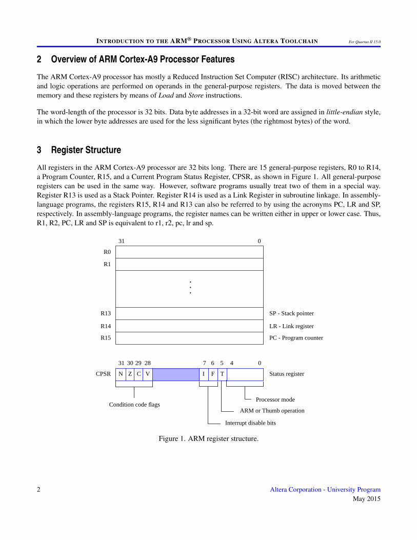
3 Register Structure
All registers in the ARM Cortex-A9 processor are 32 bits long. There are 15 general-purpose registers, R0 to R14,a Program Counter, R15, and a Current Program Status Register, CPSR, as shown in Figure 1. All general-purposeregisters can be used in the same way. However, software programs usually treat two of them in a special way.Register R13 is used as a Stack Pointer. Register R14 is used as a Link Register in subroutine linkage. In assembly-language programs, the registers R15, R14 and R13 can also be referred to by using the acronyms PC, LR and SP,respectively. In assembly-language programs, the register names can be written either in upper or lower case. Thus,R1, R2, PC, LR and SP is equivalent to r1, r2, pc, lr and sp.
•••
N Z C V
31 29 7 02830 6 45
I F T
Processor mode
ARM or Thumb operation
Interrupt disable bits
Condition code flags
031
R0
R1
R13
R14
R15
SP - Stack pointer
LR - Link register
PC - Program counter
Status registerCPSR
Figure 1. ARM register structure.
2 Altera Corporation - University ProgramMay 2015
INTRODUCTION TO THE ARM® PROCESSOR USING ALTERA TOOLCHAIN For Quartus II 15.0
The CPSR register has the following contents:
• Condition Code flags which are set based on the results of a previous operation. Most ARM instructions canbe executed conditionally based on the values of these flags:
– Negative (N) - set to 1 if the result is negative; otherwise, cleared to 0
– Zero (Z) - set to 1 if the result is 0; otherwise, cleared to 0.
– Carry (C) - set to 1 if a carry-out results from the operation; otherwise, cleared to 0.
– Overflow (V) - set to 1 if arithmetic overflow occurs; otherwise cleared to 0.
• Interrupt-disable bits, I and F, where
– I = 1 disables the IRQ interrupts
– F = 1 disables FIQ interrupts
• Thumb bit, where
– T = 0 indicates ARM execution
– T = 1 indicates Thumb execution
• Processor mode bits which identify the mode in which the processor is operating, as explained in Section 9.
For some registers, there are duplicate registers, called banked registers, for saving the contents of primary registerswhen various types of interrupts occur, as discussed in Section 10.
4 Instruction Sets
The ARM Cortex-A9 processor can execute instructions in three different instruction sets, known as ARM, Thumband Thumb-2.
The ARM set is the most powerful. All instructions are 32 bits long. The instructions are stored in memory inword-aligned manner.
The Thumb set is a smaller version, where the instructions are provided in a format that uses only 16 bits. Thisusually results in smaller memory requirements, which can be useful in embedded applications.
The Thumb-2 set includes both 16- and 32-bit instructions. Its functionality is almost identical to that of the ARMinstruction set.
In this tutorial we will deal only with the ARM instruction set. We should note that there exists a Unified AssemblerLanguage (UAL), which provides a common syntax for ARM and Thumb instructions. It supersedes the previousversions of both the ARM and Thumb assembler languages. We will use UAL in this tutorial.
Altera Corporation - University ProgramMay 2015
3
INTRODUCTION TO THE ARM® PROCESSOR USING ALTERA TOOLCHAIN For Quartus II 15.0
5 Accessing Memory and I/O Devices
Any input/output devices that can be accessed by the ARM processor are memory mapped and can be accessedas memory locations. Data accesses to memory locations and I/O interfaces are performed by means of Load andStore instructions, which cause data to be transferred between the memory and general-purpose registers. The ARMprocessor issues 32-bit addresses. The memory space is byte-addressable. Instructions can read and write words (32bits), halfwords (16 bits), or bytes (8 bits) of data.
5.1 Addressing Modes for Load and Store Instructions
The Load and Store instructions are the only type of instructions that can access memory locations. Load instructionscopy the contents of a memory location specified by an addressing mode into a destination register, which is ageneral-purpose register, Rd . Store instructions copy the contents of a general-purpose register, Rd , into a memorylocation specified by an addressing mode.
An addressing mode provides the information needed to determine the address of the desired memory location.There are different ways of specifying the required address. All addressing modes involve one or two general-purpose registers, plus some additional information. One register is referred to as the base register, Rn. If a secondregister is used, it is referred to as the index register, Rm. The memory address is determined by adding the contentsof the base register and a value that is either given as a signed 12-bit offset directly in the instruction or as a magnitudein the index register. The magnitude in Rm can be scaled by shifting it either left or right a number of bit-positionsspecified in the instruction.
There are three primary addressing modes provided:
• Offset mode – the address is determined by adding the contents of a base register and an offset that is eithergiven directly in the instruction or in an index register.
• Pre-indexed mode – the address is determined in the same way as in the Offset mode; subsequently, thisaddress replaces the contents of the base register used.
• Post-indexed mode – the address is the contents of a base register; subsequently, the base register is loadedwith a new address that is determined in the same way as in the Offset mode.
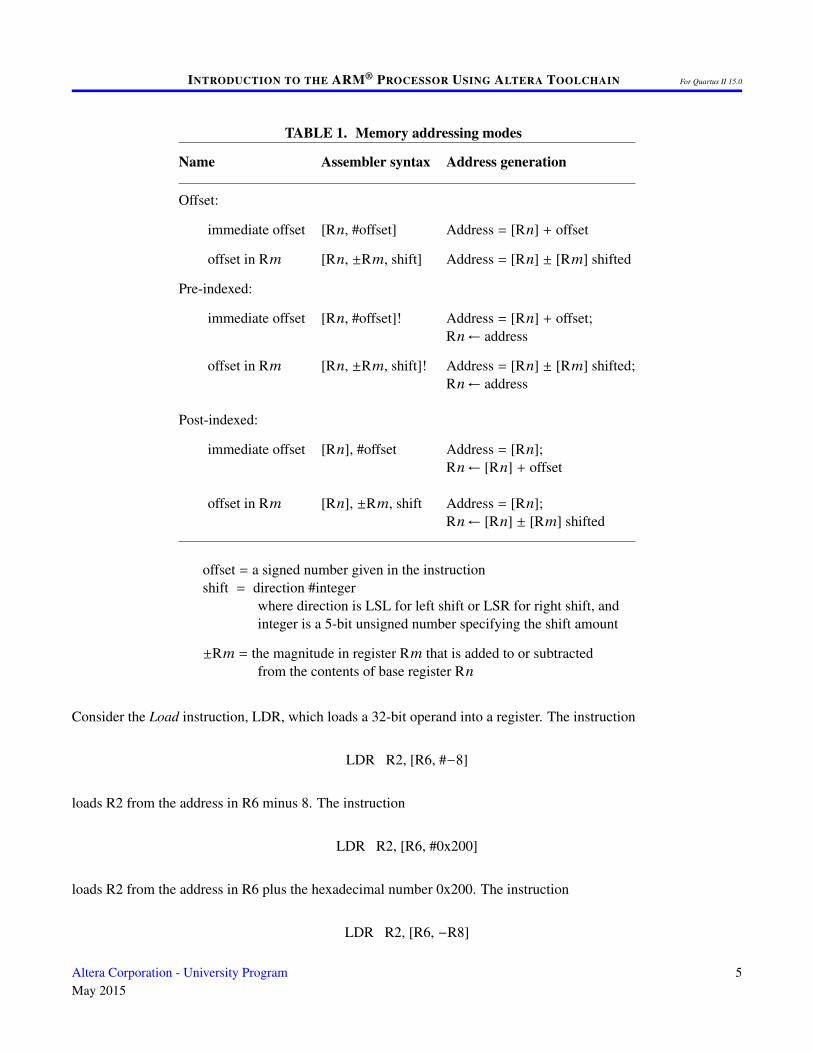
These addressing modes are fully specified in Table 1, which indicates how the address generation is performed.The table also gives the required Assembler syntax.
When an index register is specified, its contents are interpreted as a magnitude which can be either added to orsubtracted from a base register. This magnitude can first be shifted left or right by specifying LSL #k or LSR #k,respectively, where k is an integer from 1 to 31. Shifting operations are discussed further in section 6.7.
Since the Program Counter, R15, can be treated as a general-purpose register, it can be used in the Offset addressingmode as a base register, Rn. This makes it possible to access memory locations in terms of their distance relative tothe current address in R15. This mode is often referred to as the Relative addressing mode.
4 Altera Corporation - University ProgramMay 2015
INTRODUCTION TO THE ARM® PROCESSOR USING ALTERA TOOLCHAIN For Quartus II 15.0
TABLE 1. Memory addressing modes
Name Assembler syntax Address generation
Offset:
immediate offset [Rn, #offset] Address = [Rn] + offset
offset in Rm [Rn, ±Rm, shift] Address = [Rn] ± [Rm] shifted
Pre-indexed:
immediate offset [Rn, #offset]! Address = [Rn] + offset;Rn ← address
offset in Rm [Rn, ±Rm, shift]! Address = [Rn] ± [Rm] shifted;Rn ← address
Post-indexed:
immediate offset [Rn], #offset Address = [Rn];Rn ← [Rn] + offset
offset in Rm [Rn], ±Rm, shift Address = [Rn];Rn ← [Rn] ± [Rm] shifted
offset = a signed number given in the instructionshift = direction #integer
where direction is LSL for left shift or LSR for right shift, andinteger is a 5-bit unsigned number specifying the shift amount
±Rm = the magnitude in register Rm that is added to or subtractedfrom the contents of base register Rn
Consider the Load instruction, LDR, which loads a 32-bit operand into a register. The instruction
LDR R2, [R6, #−8]
loads R2 from the address in R6 minus 8. The instruction
LDR R2, [R6, #0x200]
loads R2 from the address in R6 plus the hexadecimal number 0x200. The instruction
LDR R2, [R6, −R8]
Altera Corporation - University ProgramMay 2015
5
INTRODUCTION TO THE ARM® PROCESSOR USING ALTERA TOOLCHAIN For Quartus II 15.0
loads R2 from the address obtained by subtracting the contents of R8 from the contents of R6.
The Pre-indexed mode is illustrated in
LDR R2, [R6, R8, LSL #4]!
which loads R2 from the location whose address is determined by shifting the contents of R8 to the left by 4 bit-positions (which is equivalent to multiplying by 16) and adding the result to the contents of R6. Subsequently, thegenerated address is loaded into R6.
An example of Post-indexed mode is
LDR R2, [R6], #20
where R6 contains the address of the location from which an operand is loaded into R2. Subsequently, the contentsof R6 are modified by adding to them the offset value 20.
Relative addressing can be used simply by specifying the address label associated with the desired memory location.For example, if MEMLOC is the desired location, then the instruction
LDR R2, MEMLOC
will load the contents of memory location MEMLOC into register R2. The assembler will determine the immediateoffset as the difference between the address MEMLOC and the contents of the updated Program Counter. It willgenerate the instruction
LDR R2, [R15, #offset]
This offset takes into account the fact that when the instruction is to be executed, the Program Counter will alreadybe incremented by 8, because the ARM processor will already have fetched the next instruction (due to pipelinedexecution).
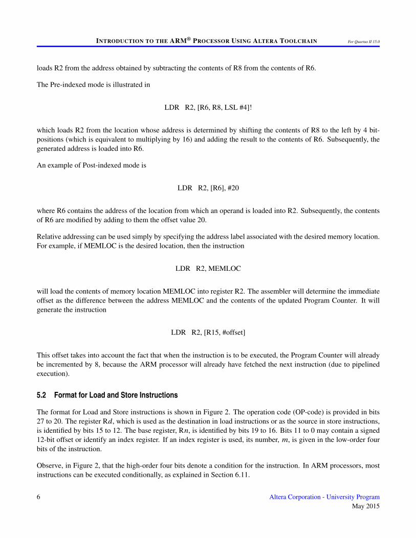
5.2 Format for Load and Store Instructions
The format for Load and Store instructions is shown in Figure 2. The operation code (OP-code) is provided in bits27 to 20. The register Rd , which is used as the destination in load instructions or as the source in store instructions,is identified by bits 15 to 12. The base register, Rn, is identified by bits 19 to 16. Bits 11 to 0 may contain a signed12-bit offset or identify an index register. If an index register is used, its number, m, is given in the low-order fourbits of the instruction.
Observe, in Figure 2, that the high-order four bits denote a condition for the instruction. In ARM processors, mostinstructions can be executed conditionally, as explained in Section 6.11.
6 Altera Corporation - University ProgramMay 2015
INTRODUCTION TO THE ARM® PROCESSOR USING ALTERA TOOLCHAIN For Quartus II 15.0
31 028
Condition
27 1120 19 16 15 12
OP code Rn Rd Offset or Rm
Figure 2. Format for Load and Store instructions.
6 ARM Instructions
ARM instructions are 32-bits long. In addition to machine instructions that are executed directly by the processor,the ARM instruction set includes a number of pseudo-instructions that can be used in assembly language programs.The Assembler replaces each pseudo-instruction by one or more machine instructions.
This section discusses briefly the main features of the ARM instruction set. For a complete description of the instruc-tion set, including the details of how each instruction is encoded, the reader should consult the ARM ArchitectureReference Manual.
6.1 Load and Store Instructions
Load and store instructions are used to move data between memory (and I/0 interfaces) and the general-purposeregisters. The LDR (Load Register) instruction, illustrated in the previous section, loads a 32-bit operand into aregister. The corresponding Store instruction is STR (Store Register). For example,
STR R2, [R4]
copies the contents of R2 into memory location at the address that is found in register R4.
There are also load and store instructions that use operands that are only 8 or 16 bits long. They are referred to asLoad/Store Byte and Load/Store Halfword instructions, respectively. Such load instructions are:
• LDRB (Load Register Byte)
• LDRSB (Load Register Signed Byte)
• LDRH (Load Register Halfword)
• LDRSH (Load Register Signed Halfword)
When a shorter operand is loaded into a 32-bit register, its value has to be adjusted to fit into the register. This isdone by zero-extending the 8- or 16-bit value to 32 bits in the LDRB and LDRH instructions. In the LDRSB andLDRSH instructions the operand is sign-extended.
The corresponding Store instructions are:
• STRB (Store Register Byte)
Altera Corporation - University ProgramMay 2015
7
INTRODUCTION TO THE ARM® PROCESSOR USING ALTERA TOOLCHAIN For Quartus II 15.0
• STRH (Store Register Halfword)
The STRB instruction stores the low byte of register Rd into the memory byte specified by the address. The STRHinstruction stores the low halfword of register Rd .
6.1.1 Loading and Storing Multiple Registers
There are two instructions that allow loading of data into multiple registers, LDM (Load Multiple), and storing thecontents of multiple registers into memory, STM (Store Multiple). The memory operands must be in successiveword locations. These instructions are useful for two main purposes:
• transferring blocks of data between memory and processor registers, and
• saving data in registers on a stack when subroutines are used.
The address of the first word in memory is given in the base register, Rn. Upon transferring the last word of data,the contents of Rn can be updated with the last address by specifying the Pre-indexed addressing mode.
An instruction must specify the registers involved in the transfer. The registers must be listed in ascending order inthe assembly-language instruction, in a field enclosed by braces, but they do not have to be contiguous. A range ofregisters is specified by listing the first and the last registers in the range, separated by a dash (−). In the resultingmachine instruction, each register is identified by setting a corresponding bit in the field comprising the low-order16 bits.
The instruction must also indicate the direction in which memory addresses are computed. For block transfers thereare four possibilities for determining the addresses of consecutive data words. The address can be incremented ordecremented by 4 either before or after each data item is accessed. The desired action is specified by appending asuffix to the OP-code mnemonic in the assembly-language instruction. The four suffixes are:
• IA – Increment After
• IB – Increment Before
• DA – Decrement After
• DB – Decrement Before
For example, the instruction
LDMIA R3!, {R4, R6−R8, R10}
will load registers R4, R6, R7, R8 and R10. If the starting address in R3 is 1000, then the data loaded into theregisters will be from addresses 1000, 1004, 1008, 1012 and 1016, respectively. Because the Pre-indexed mode isspecified, the final contents of R3 will be 1020.
8 Altera Corporation - University ProgramMay 2015
INTRODUCTION TO THE ARM® PROCESSOR USING ALTERA TOOLCHAIN For Quartus II 15.0
The LDM and STM instructions are very useful in the context of subroutines, where they can be used to savethe contents of registers on the stack. For this purpose, there exist pseudo-instructions PUSH and POP, which areactually implemented as particular forms of STM and LDM instructions. In these instructions the Stack Pointer, SP,is the base register, which is always updated. The SP is decremented by 4 before each transfer in PUSH instructions,and it is incremented by 4 after each transfer in POP instructions. For example, the instruction
PUSH {R1, R3−R5}
places the contents of registers R1, R3, R4 and R5 on the stack. The equivalent Store Multiple instruction would be
STMDB SP!, {R1, R3−R5}
The instruction
POP {R1, R3−R5}
restores the contents of these registers from the stack. The equivalent Load Multiple instruction would be
LDMIA SP!, {R1, R3−R5}
6.2 Data Processing Instructions
A variety of ARM instructions are provided for the processing of data, including instructions that perform shifting,arithmetic operations, logical operations, and data transfer between registers.
6.3 Flexible Operands
A number of data processing instruction have the general form
OP Rd , Rn, Operand2
where Rd is the destination register, Rn is the first operand, and Operand2 is the second operand. A considerableamount of flexibility is provided by Operand2. It can be an immediate constant, as in
OP Rd , Rn, #value
This instruction performs the operation OP using the contents of Rn and the constant value, and places the resultinto Rd . For example, if OP is the addition instruction ADD, then
ADD R0, R1, #1
Altera Corporation - University ProgramMay 2015
9
INTRODUCTION TO THE ARM® PROCESSOR USING ALTERA TOOLCHAIN For Quartus II 15.0
adds 1 to the contents of R1 and places the sum into R0. The constant value can be specified as a decimal number,as in this example, or as a binary value #0b1, or as a hexadecimal value #0x1. Valid constants include any eight-bitvalue, such as 0xFF. The eight-bit value can also be produced by rotation in a 32-bit word—for example, other validconstants include 0xFF000000, 0xFF0000, and 0xFF00. In general, the constant can be any value which can begenerated by rotating a byte to the right any even number of times (0, 2, . . ., 30) in a 32-bit word (see the ARMAssembler Reference for more details).
Alternatively, Operand2 can be given as a register Rm, as in
OP Rd , Rn, Rm
This instruction performs the operation OP using the contents of Rn and Rm, and places the result into Rd . Forexample
ADD R0, R1, R2
adds the contents of R1 and R2, and places the sum into R0.
When Operand2 is a register, Rm can either be used directly, as in the above example, or else its value can be shiftedbefore being used. If it is shifted, then the shifting amount can be specified as a five-bit constant, as in
OP Rd , Rn, Rm, LSL #3
or as the least-significant byte of a register Rs, as in
OP Rd , Rn, Rm, LSL Rs
In these examples LSL means Logical Shift Left. Other examples of shift variants include right-shift, and rotateoperations, as discussed in section 6.7.
6.3.1 Using Condition Code Flags
The data processing instructions can optionally affect the ARM condition code flags, or can be executed conditionallybased on the values of the condition code flags. These options are expressed in the general form
OP{S}{cond} Rd , Rn, Operand2
If S is included in the instruction mnemonic, as in ADDS, then the condition code flags will be set depending on theresults of the instruction. But if S is not included, as in ADD, then the flags are unaffected by the instruction. Settingof the condition code flags is discussed further in Section 6.9.
An optional cond appended to an instruction mnemonic allows an instruction to be either executed or skipped,depending on the current values of the condition code flags. This concept is discussed in Section 6.10.
10 Altera Corporation - University ProgramMay 2015
INTRODUCTION TO THE ARM® PROCESSOR USING ALTERA TOOLCHAIN For Quartus II 15.0
6.4 Arithmetic Instructions
As illustrated above, an arithmetic operation such as
ADD Rd , Rn, Operand2
adds the contents of Rn and the value determined as Operand2 into Rd . For example, the instruction
ADD R0, R1, R2, LSL #2
adds the contents of R1 and a shifted version of the contents of R2, and places the sum into R0. The operand R2is shifted to the left by 2 bit positions (which is equivalent to integer multiplication by 4) before it is used in theaddition.
In an assembly-language instruction, it is possible to specify a negative number as the immediate operand, as in
ADD R0, R1, #−24
The Assembler will implement this operation with the Subtract instruction
SUB R0, R1, #24
6.4.1 Multiplication
There are two versions of multiplication instructions:
• MUL – (Multiply)
• MLA – (Multiply Accumulate)
The Multiply instruction
MUL R2, R4, R5
multiplies the contents of registers R4 and R5, and places a 32-bit product into register R2. If the generated productexceeds 32 bits, then the low-order 32 bits are retained and the high-order bits are discarded.
The MLA instruction multiplies the operands in two registers to produce a 32-bit product, which is then added tothe third operand, and the result is written into the destination register. Thus,
MLA R2, R4, R5, R6
multiplies the numbers in R4 and R5, adds to this product the number in R6, and places the result into register R2.
Altera Corporation - University ProgramMay 2015
11
INTRODUCTION TO THE ARM® PROCESSOR USING ALTERA TOOLCHAIN For Quartus II 15.0
6.5 Logic and Test Instructions
The logic instructions provide the AND, OR and Exclusive-OR operations. The AND instruction
AND Rd , Rn, Operand2
performs a bitwise logical AND of the contents of register Rn with the value of Operand2, and stores the result inregister Rd . Similarly, the instructions ORR and EOR perform the OR and Exclusive-OR operations, respectively.
Another useful logic instruction is BIC, which stands for Bit Clear. It performs a bitwise AND of the operand in Rnwith the complement of Operand2, and stores the result in Rd .
There are two instructions that perform logic operations for testing purposes. The Test instruction
TST Rn, Operand2
performs the AND operation using the contents of Rn and Operand2, and sets the condition code flags based on theresult obtained. The Test Equivalence instruction
TEQ Rn, Operand2
compares the value in Rn with the value represented by Operand2. This is done by exclusive-ORing the two valuesand setting the condition code flags accordingly.
6.6 Move Instructions
The Move instructions copy the contents of one register into another, or they place an immediate value into a register.
The Move instruction
MOV Rd , Operand2
moves the value of Operand2 into register Rd .
The Move Negative instruction
MVN Rd , Operand2
moves the complement of the value of Operand2 into Rd .
The Move Top instruction
12 Altera Corporation - University ProgramMay 2015
INTRODUCTION TO THE ARM® PROCESSOR USING ALTERA TOOLCHAIN For Quartus II 15.0
MOVT Rd , #immed16
loads a 16-bit immediate value into the high-order 16 bits of Rd , and leaves the low-order 16 bits unchanged.
There are also two special instructions, MRS and MSR, which copy the contents of a processor status register to/froma general-purpose register. These instructions are available only when the processor is running in a privileged mode,as explained in Section 10.
6.6.1 Loading 32-bit Constants into Registers
The simplest approach is to use the load-register pseudo-instruction
LDR R2, =0x12345678
in which case the Assembler will place this constant, and other constants defined in such manner, into a literal poolin the memory, from where it will be taken at execution time. In the assembled code, this LDR instruction will usethe Relative addressing mode to access the literal pool. The Assembler decides where in memory to place the literalpool; typically, it is immediately following the program’s machine code.
A constant may be represented by a name, say LABEL. For example, LABEL may correspond to the address ofsome memory location. In that case, this address can be loaded into a register, Rd , using the pseudo-instruction
LDR Rd , =LABEL
Again, the Assembler will place the corresponding 32-bit address into the literal pool.
6.7 Shift and Rotate Instructions
ARM has shift and rotate instruction mnemonics:
• LSL – Logical Shift Left
• LSR – Logical Shift Right
• ASR – Arithmetic Shift Right
• ROR – Rotate Right
An example of a shift instruction is
LSL R2, R5, #4
which shifts the value in R5 to the left by four bit-positions (zeros are inserted on the right) and places the result intoR2. Since Operand2 of any instruction can be shifted or rotated, it is possible to use Move instructions mnemonicsinstead of shift and rotate. For example, the instruction
Altera Corporation - University ProgramMay 2015
13
INTRODUCTION TO THE ARM® PROCESSOR USING ALTERA TOOLCHAIN For Quartus II 15.0
MOV R2, R5, LSL #4
is equivalent to the LSL instruction shown above. Also, the same effect can be achieved with the instruction
LSL R2, R5, R6
if the contents of R6 are equal to 4. There is also a logical shift right, LSR, instruction, in which bits are shifted tothe right with zeros being inserted on the left. Similarly, arithmetic shift right, ASR, performs a shift to the right, butin this case the sign bit, b31, is replicated on the left for each shift position. Another example is
ROR R3, R3, #8
which rotates the contents of R3 to the right by eight bit-positions. In the rotate instruction bits shifted out of positionb0 on the right are inserted into position b31 on the left, in a circular fashion.
6.8 Comparison Instructions
The comparison instructions compare the contents of two registers or the contents of a register and an immediatevalue, and set the condition code flags based on the result.
The Compare instruction
CMP Rn, Operand2
performs the comparison by subtracting the value of Operand2 from the value in Rn. It sets the condition code flags,but it does not change the contents of Rn.
The Compare Negative instruction
CMN Rn, Operand2
performs the comparison by adding the value of Operand2 and the value in Rn. It sets the condition code flags, butit does not change the contents of Rn.
6.9 Setting of Condition Code Flags
The condition code flags are always affected by the compare instructions, CMP and CMN, and the test instructions,TST and TEQ. Many other instructions can also affect the condition code flags, but this must be specified in theinstruction. The data processing instructions (arithmetic, logic and move) affect these flags if the suffix S is appendedto the assembly-language OP-code mnemonic, as we mentioned in Section 6.3.1.
For example, the instruction
14 Altera Corporation - University ProgramMay 2015
INTRODUCTION TO THE ARM® PROCESSOR USING ALTERA TOOLCHAIN For Quartus II 15.0
ADDS R2, R3, R4
will set the flags, but
ADD R2, R3, R4
will not.
6.10 Conditional Execution of Instructions
Most ARM instructions can be executed conditionally. The high-order four bits in the machine representation ofeach instruction, as illustrated in Figure 2, specify a condition that must be met for the instruction to be executed.These conditions are associated with the condition code flags N, Z, C and V. The instruction is executed only if thereis a match between the specified condition and the current values of the condition code flags.
The general form of data processing instructions is
OP{S}{cond} Rd , Rn, Operand2
The conditions that can be specified are those in Table 2. Observe that there are 14 patterns for conditions thatdepend on the condition code flags.
For example, the instruction
ADDEQ R2, R3, R4
will be executed if the condition code flag Z is equal to 1. Otherwise, the execution will skip to the next instruction.
The instruction
MOVNE R1, R0
Will transfer the contents of R0 into R1 if the current value of the Z flag is 0. If Z = 1, the Move instruction will notbe executed and the processor will skip to the next instruction.
6.11 Branch Instructions
The flow of execution of a program can be changed by executing a Branch instruction. It may be changed eitherconditionally or unconditionally.
A branch instruction is specified as
Altera Corporation - University ProgramMay 2015
15
INTRODUCTION TO THE ARM® PROCESSOR USING ALTERA TOOLCHAIN For Quartus II 15.0
B{cond_suffix} LABEL
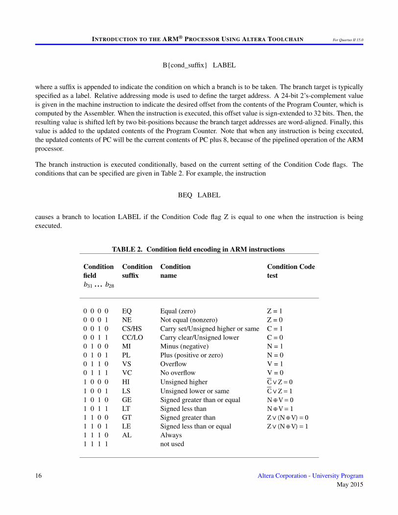
where a suffix is appended to indicate the condition on which a branch is to be taken. The branch target is typicallyspecified as a label. Relative addressing mode is used to define the target address. A 24-bit 2’s-complement valueis given in the machine instruction to indicate the desired offset from the contents of the Program Counter, which iscomputed by the Assembler. When the instruction is executed, this offset value is sign-extended to 32 bits. Then, theresulting value is shifted left by two bit-positions because the branch target addresses are word-aligned. Finally, thisvalue is added to the updated contents of the Program Counter. Note that when any instruction is being executed,the updated contents of PC will be the current contents of PC plus 8, because of the pipelined operation of the ARMprocessor.
The branch instruction is executed conditionally, based on the current setting of the Condition Code flags. Theconditions that can be specified are given in Table 2. For example, the instruction
BEQ LABEL
causes a branch to location LABEL if the Condition Code flag Z is equal to one when the instruction is beingexecuted.
TABLE 2. Condition field encoding in ARM instructions
Condition Condition Condition Condition Codefield suffix name testb31 . . . b28
0 0 0 0 EQ Equal (zero) Z = 10 0 0 1 NE Not equal (nonzero) Z = 00 0 1 0 CS/HS Carry set/Unsigned higher or same C = 10 0 1 1 CC/LO Carry clear/Unsigned lower C = 00 1 0 0 MI Minus (negative) N = 10 1 0 1 PL Plus (positive or zero) N = 00 1 1 0 VS Overflow V = 10 1 1 1 VC No overflow V = 01 0 0 0 HI Unsigned higher C∨Z = 01 0 0 1 LS Unsigned lower or same C∨Z = 11 0 1 0 GE Signed greater than or equal N⊕V = 01 0 1 1 LT Signed less than N⊕V = 11 1 0 0 GT Signed greater than Z∨ (N⊕V) = 01 1 0 1 LE Signed less than or equal Z∨ (N⊕V) = 11 1 1 0 AL Always1 1 1 1 not used
16 Altera Corporation - University ProgramMay 2015
INTRODUCTION TO THE ARM® PROCESSOR USING ALTERA TOOLCHAIN For Quartus II 15.0
The suffix AL (Always) causes the unconditional branch. The same effect is achieved if there is no suffix appended.The Assembler interprets the instruction
B LABEL
as being the same as
BAL LABEL
6.12 Subroutine Linkage Instructions
Subroutine calls are achieved with the Branch and Link instruction
BL Destination
where the Destination is typically the label of the first instruction in the subroutine. In addition to behaving as aBranch instruction, this instruction saves the return address (which is the address of the instruction that follows theBL instruction) in the Link register, R14.
There is no specific return-from-subroutine instruction. The return from a subroutine can be performed by an in-struction that loads the contents of R14 into R15, such as
MOV PC, LR
Since LR can hold only one return address, it follows that if nested subroutines are used it is necessary to save thecontents of R14, typically on the stack, prior to a nested subroutine call.
We should also mention that in the ARM environment, there is a convention that registers R0 to R4 are used to passparameters to a subroutine, while register R0 is used to return a result. If more than four parameters are needed, thensome of the parameters have to be passed via the stack.
7 Assembler Directives
Assembler directives provide information used by the assembler when assembling an application program. Differentassemblers often use different assembler directives. We will restrict our discussion to the assembler that is used bythe Altera Monitor Program. This assembler conforms to the widely used GNU Assembler, which is softwareavailable in the public domain. Thus, the GNU Assembler directives can be used in ARM programs intended to beused with the Altera Monitor Program.
Assembler directives begin with a period. We describe some of the more frequently used assembler directives below.
Altera Corporation - University ProgramMay 2015
17
INTRODUCTION TO THE ARM® PROCESSOR USING ALTERA TOOLCHAIN For Quartus II 15.0
.ascii "string"
A string of ASCII characters is loaded into consecutive byte addresses in the memory. Multiple strings, separatedby commas, can be specified. The directive .asciz is the same, except that each string is terminated by a zero byte.
.byte expressions
Expressions separated by commas are specified. Each expression is assembled into the next byte. Examples ofexpressions are: 8, 5 + LABEL, and K − 6.
.end
Marks the end of the source code file; everything after this directive is ignored by the assembler.
.equ symbol, expression
Sets the value of symbol to expression.
.global symbol
Makes symbol visible outside the assembled object file.
.hword expressions
Expressions separated by commas are specified. Each expression is assembled into a 16-bit number.
.include "filename"
Provides a mechanism for including supporting files in a source program.
.section arguments
Allows a named section to be created in the assembly language file. This directive is used, for example, whenspecifying exception vectors.
.skip size
Emits the number of bytes specified in size; the value of each byte is zero.
.text
Identifies the code that should be placed in the text section of the memory. The desired memory location for the textsection can be specified in the Altera Monitor Program’s system configuration window.
.word expressions
Expressions separated by commas are specified. Each expression is assembled into a 32-bit number.
18 Altera Corporation - University ProgramMay 2015
INTRODUCTION TO THE ARM® PROCESSOR USING ALTERA TOOLCHAIN For Quartus II 15.0
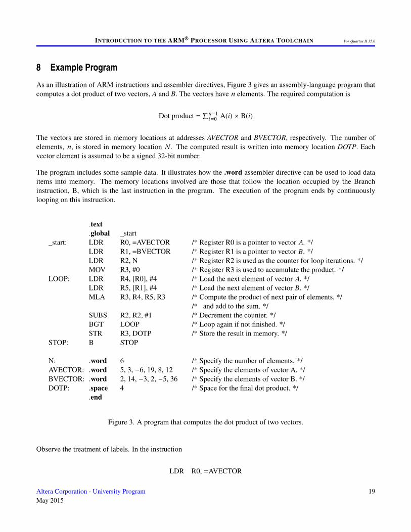
8 Example Program
As an illustration of ARM instructions and assembler directives, Figure 3 gives an assembly-language program thatcomputes a dot product of two vectors, A and B. The vectors have n elements. The required computation is
Dot product = ∑n−1i=0 A(i) × B(i)
The vectors are stored in memory locations at addresses AVECTOR and BVECTOR, respectively. The number ofelements, n, is stored in memory location N . The computed result is written into memory location DOTP. Eachvector element is assumed to be a signed 32-bit number.
The program includes some sample data. It illustrates how the .word assembler directive can be used to load dataitems into memory. The memory locations involved are those that follow the location occupied by the Branchinstruction, B, which is the last instruction in the program. The execution of the program ends by continuouslylooping on this instruction.
.text
.global _start_start: LDR R0, =AVECTOR /* Register R0 is a pointer to vector A. */
LDR R1, =BVECTOR /* Register R1 is a pointer to vector B . */LDR R2, N /* Register R2 is used as the counter for loop iterations. */MOV R3, #0 /* Register R3 is used to accumulate the product. */
LOOP: LDR R4, [R0], #4 /* Load the next element of vector A. */LDR R5, [R1], #4 /* Load the next element of vector B . */MLA R3, R4, R5, R3 /* Compute the product of next pair of elements, */
/* and add to the sum. */SUBS R2, R2, #1 /* Decrement the counter. */BGT LOOP /* Loop again if not finished. */STR R3, DOTP /* Store the result in memory. */
STOP: B STOP
N: .word 6 /* Specify the number of elements. */AVECTOR: .word 5, 3, −6, 19, 8, 12 /* Specify the elements of vector A. */BVECTOR: .word 2, 14, −3, 2, −5, 36 /* Specify the elements of vector B. */DOTP: .space 4 /* Space for the final dot product. */
.end
Figure 3. A program that computes the dot product of two vectors.
Observe the treatment of labels. In the instruction
LDR R0, =AVECTOR
Altera Corporation - University ProgramMay 2015
19
INTRODUCTION TO THE ARM® PROCESSOR USING ALTERA TOOLCHAIN For Quartus II 15.0
a 32-bit address that denotes the location AVECTOR is loaded into register R0, as explained in Section 6.6.1 But, inthe instruction
LDR R2, N
it is the value 6, which is stored at location N, that is loaded into register R2. In both cases, the assembled LDRmachine instruction will use Relative addressing to access the source operand.
9 Operating Modes
The ARM processor can operate in a number of different modes, as follows:
• User mode – is the basic mode in which application programs run. This is an unprivileged mode, which hasrestricted access to system resources.
• System mode – provides full access to system resources. It can be entered only from one of the exceptionmodes listed below.
• Supervisor mode – is entered when a software interrupt is raised by a program executing a Supervisor Callinstruction, SVC. It is also entered on reset or power-up.
• Abort mode – is entered if a program attempts to access a non-existing memory location.
• Undefined mode – is entered if the processor attempts to execute an unimplemented instruction.
• IRQ mode – is entered in response to a normal interrupt request from an external device.
• FIQ mode – is entered in response to a fast interrupt request from an external device. It is used to providefaster service for more urgent requests.
The User mode is unprivileged, and all other modes are privileged. In order to manipulate the contents of theprocessor status register, the processor must be in one of the privileged modes. The User and System modes usethe registers presented in Figure 1. Other modes, which deal with various exceptions, use some other registers, asdescribed in the next section.
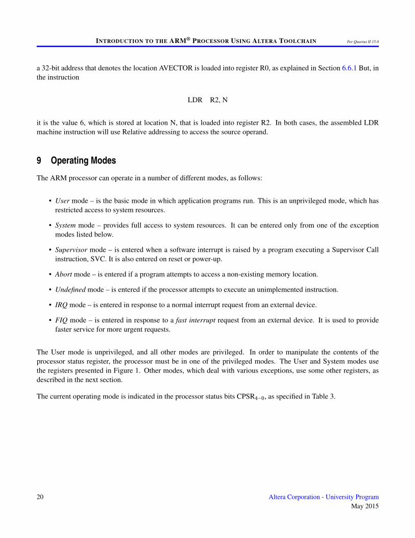
The current operating mode is indicated in the processor status bits CPSR4−0, as specified in Table 3.
20 Altera Corporation - University ProgramMay 2015
INTRODUCTION TO THE ARM® PROCESSOR USING ALTERA TOOLCHAIN For Quartus II 15.0
TABLE 3. Operating Mode Assignment
CPSR4−0 Operating Mode
10000 User10001 FIQ10010 IRQ10011 Supervisor10111 Abort11011 Undefined11111 System
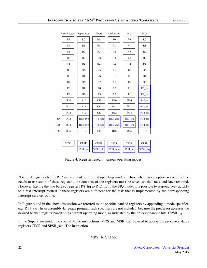
10 Banked Registers
To make the processing of exceptions more efficient, some other registers are involved. These registers are shown inblue in Figure 4. They are called the banked registers. There is a different set of banked registers for each exceptionmode. All exception modes use their own versions of the Stack Pointer, SP_mode, the Link register, LR_mode, andthe Status register, SPSR_mode. The FIQ mode also has its own registers R8 to R12, which are called R8_fiq toR12_fiq in the figure.
Altera Corporation - University ProgramMay 2015
21
INTRODUCTION TO THE ARM® PROCESSOR USING ALTERA TOOLCHAIN For Quartus II 15.0
R0
R1
R2
R3
R4
R5
R6
R7
R8
R9
R10
R11
R12
R13
R14
R15
R0
R1
R2
R3
R4
R5
R6
R7
R8
R9
R10
R11
R12
R13_und
R14_und
R15
R0
R1
R2
R3
R4
R5
R6
R7
R8
R9
R10
R11
R12
R13_irq
R14_irq
R15
R0
R1
R2
R3
R4
R5
R6
R7
R8_fiq
R9_fiq
R10_fiq
R11_fiq
R12_fiq
R13_fiq
R14_fiq
R15
R0
R1
R2
R3
R4
R5
R6
R7
R8
R9
R10
R11
R12
R13_abt
R14_abt
R15
R0
R1
R2
R3
R4
R5
R6
R7
R8
R9
R10
R11
R12
R13_svc
R14_svc
R15
User/System Supervisor Abort Undefined IRQ FIQ
CPSR CPSR CPSR CPSR CPSR CPSR
SPSR_svc SPSR_abt SPSR_und SPSR_irq SPSR_fiq
SP
LR
PC
Figure 4. Registers used in various operating modes.
Note that registers R0 to R12 are not banked in most operating modes. Thus, when an exception service routineneeds to use some of these registers, the contents of the registers must be saved on the stack and later restored.However, having the five banked registers R8_fiq to R12_fiq in the FIQ mode, it is possible to respond very quicklyto a fast interrupt request if these registers are sufficient for the task that is implemented by the correspondinginterrupt-service routine.
In Figure 4 and in the above discussion we referred to the specific banked registers by appending a mode specifier,e.g. R14_svc. In an assembly-language program such specifiers are not included, because the processor accesses thedesired banked register based on its current operating mode, as indicated by the processor-mode bits, CPSR4−0.
In the Supervisor mode, the special Move instructions, MRS and MSR, can be used to access the processor statusregisters CPSR and SPSR_svc. The instruction
MRS Rd , CPSR
22 Altera Corporation - University ProgramMay 2015
INTRODUCTION TO THE ARM® PROCESSOR USING ALTERA TOOLCHAIN For Quartus II 15.0
copies the contents of CPSR into register Rd . Writing into the status registers can be done by affecting one or morefields of the register. The processor status registers have four fields of eight bits, identified by the field specifiers _f,_s, _x and _c, which correspond to PSR31−24, PSR23−16, PSR15−8 and PSR7−0, respectively. Thus, the instruction
MSR CPSR_c, Rd
copies the contents of Rd into CPSR7−0, which affects only the processor mode and interrupt disable bits. All bitscan be affected by the instruction
MSR CPSR_cxsf, Rd
We should note that the field specifiers must be used in the MSR instruction; otherwise, an error will occur at compiletime.
In an exception mode, such as IRQ, it is the banked saved status register that is accessed. Thus,
MRS Rd , SPSR
copies the contents of SPSR_irq into register Rd .
11 Exception Processing
An exception in the normal flow of program execution can be caused by:
• Software interrupt
• Hardware interrupt
• Attempted accessing of a nonexistent memory location
• Unimplemented instruction
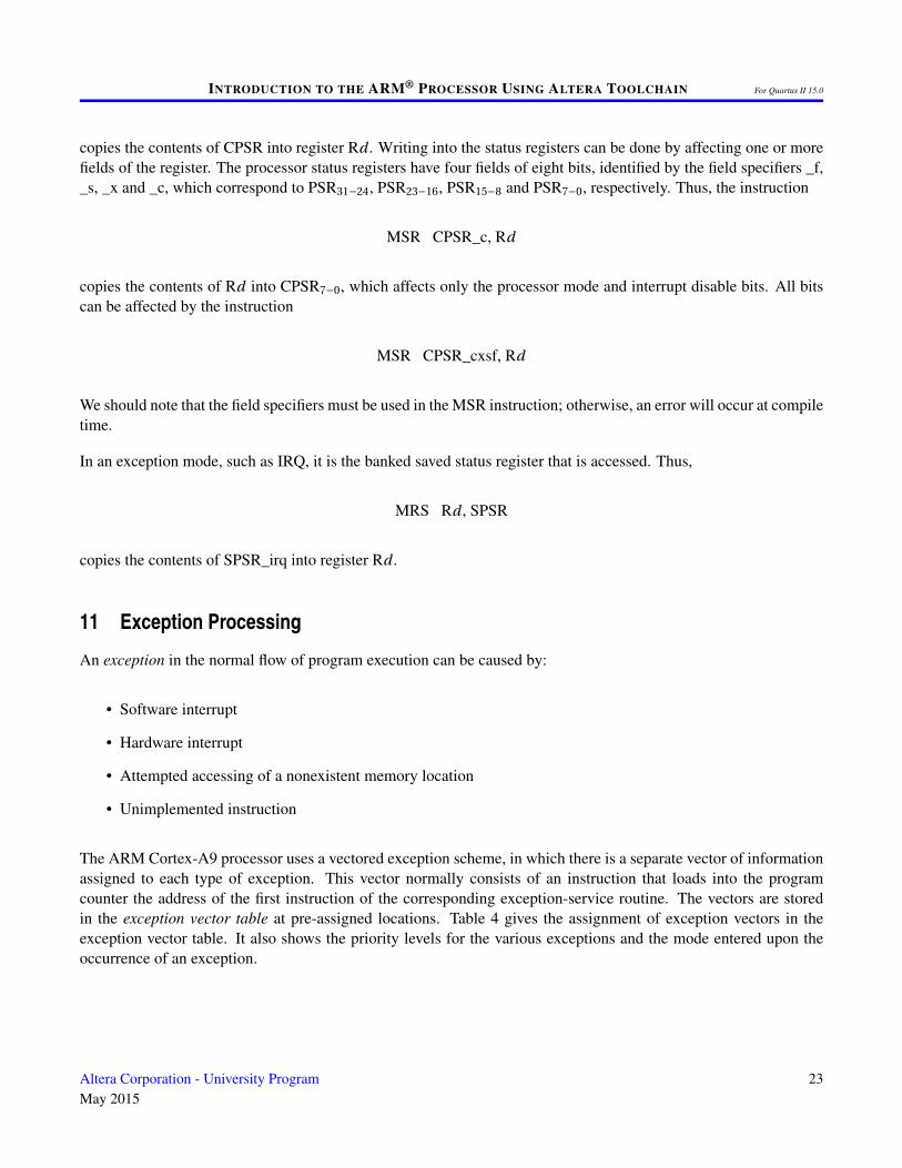
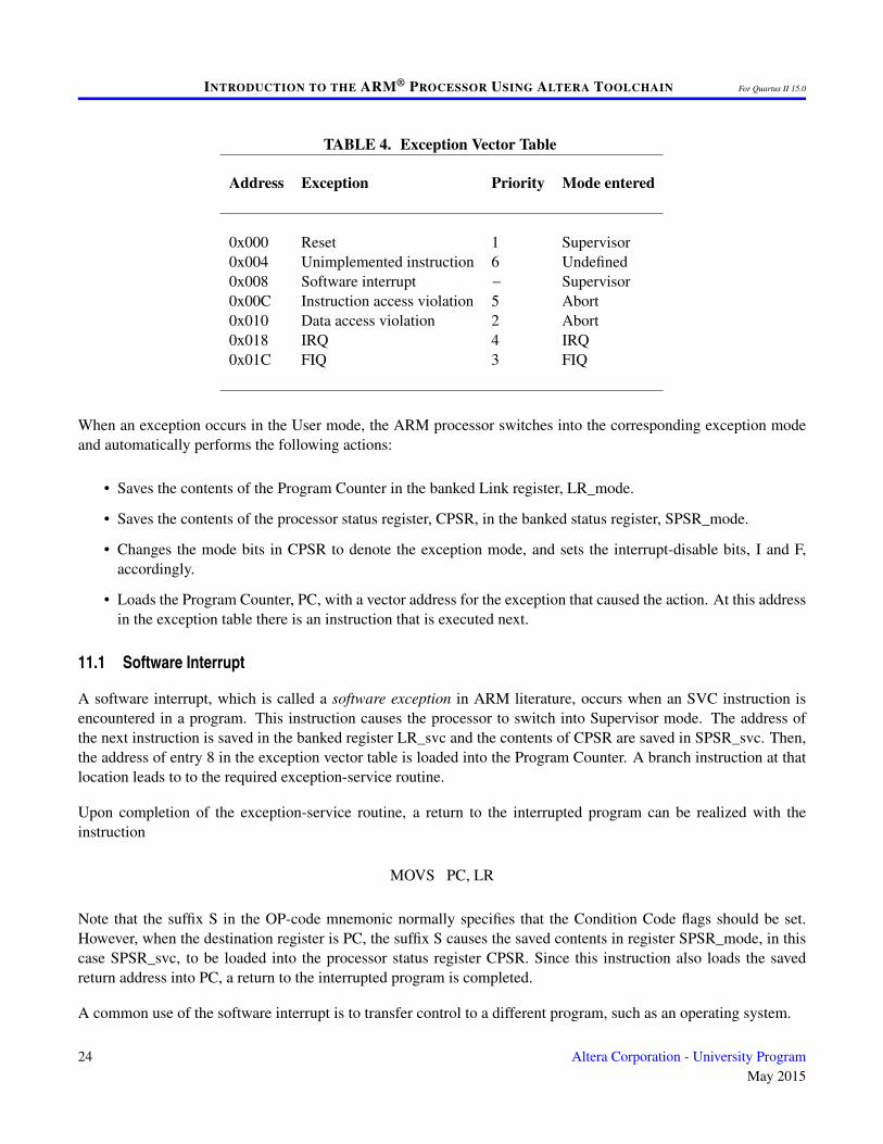
The ARM Cortex-A9 processor uses a vectored exception scheme, in which there is a separate vector of informationassigned to each type of exception. This vector normally consists of an instruction that loads into the programcounter the address of the first instruction of the corresponding exception-service routine. The vectors are storedin the exception vector table at pre-assigned locations. Table 4 gives the assignment of exception vectors in theexception vector table. It also shows the priority levels for the various exceptions and the mode entered upon theoccurrence of an exception.
Altera Corporation - University ProgramMay 2015
23
INTRODUCTION TO THE ARM® PROCESSOR USING ALTERA TOOLCHAIN For Quartus II 15.0
TABLE 4. Exception Vector Table
Address Exception Priority Mode entered
0x000 Reset 1 Supervisor0x004 Unimplemented instruction 6 Undefined0x008 Software interrupt − Supervisor0x00C Instruction access violation 5 Abort0x010 Data access violation 2 Abort0x018 IRQ 4 IRQ0x01C FIQ 3 FIQ
When an exception occurs in the User mode, the ARM processor switches into the corresponding exception modeand automatically performs the following actions:
• Saves the contents of the Program Counter in the banked Link register, LR_mode.
• Saves the contents of the processor status register, CPSR, in the banked status register, SPSR_mode.
• Changes the mode bits in CPSR to denote the exception mode, and sets the interrupt-disable bits, I and F,accordingly.
• Loads the Program Counter, PC, with a vector address for the exception that caused the action. At this addressin the exception table there is an instruction that is executed next.
11.1 Software Interrupt
A software interrupt, which is called a software exception in ARM literature, occurs when an SVC instruction isencountered in a program. This instruction causes the processor to switch into Supervisor mode. The address ofthe next instruction is saved in the banked register LR_svc and the contents of CPSR are saved in SPSR_svc. Then,the address of entry 8 in the exception vector table is loaded into the Program Counter. A branch instruction at thatlocation leads to to the required exception-service routine.
Upon completion of the exception-service routine, a return to the interrupted program can be realized with theinstruction
MOVS PC, LR
Note that the suffix S in the OP-code mnemonic normally specifies that the Condition Code flags should be set.However, when the destination register is PC, the suffix S causes the saved contents in register SPSR_mode, in thiscase SPSR_svc, to be loaded into the processor status register CPSR. Since this instruction also loads the savedreturn address into PC, a return to the interrupted program is completed.
A common use of the software interrupt is to transfer control to a different program, such as an operating system.
24 Altera Corporation - University ProgramMay 2015
INTRODUCTION TO THE ARM® PROCESSOR USING ALTERA TOOLCHAIN For Quartus II 15.0
11.2 Hardware Interrupts
Hardware interrupts can be raised by external sources, such as I/O devices, by asserting one of the processor’sinterrupt-request inputs, IRQ or FIQ. When the processor receives a hardware interrupt request, it enters the corre-sponding exception mode to service the interrupt. It also saves the contents of PC and CPSR.
The saved contents of the PC are supposed to be the return address. However, this is not the case with the ARMCortex-A9 processor. This processor prefetches instructions for execution. While the current instruction is beingexecuted, the next instruction is prefetched and its processing is started. This means that the Program Counterpoints to the instruction after the prefetched one. Namely, the updated contents of PC are the address of the currentinstruction plus 8. Since the interrupt is serviced upon completion of the current instruction, the next prefetchedinstruction is discarded and it must be executed upon return from the interrupt. Therefore, the address saved in thelink register must be decremented by 4 prior to returning to the interrupted program. This can be done by having
SUBS PC, LR, #4
as the last instruction in the exception-service routine. Note that the suffix S causes a proper return to the interruptedprogram, as explained above.
11.2.1 IRQ Interrupts
Upon accepting an IRQ interrupt request, the processor saves the contents of CPSR in the SPSR_irq register, and itsaves the contents of PC in the link register LR_irq. It also sets the mode bits in CPSR to denote the IRQ exceptionmode, and it sets the I bit to 1 to disable further IRQ interrupts. Then, it executes the instruction at location 0x018of the exception vector table, which has to cause a branch that leads to the IRQ exception-service routine.
The return from the exception-service routine should be performed with the instruction
SUBS PC, LR, #4
11.2.2 FIQ Interrupts
An FIQ interrupt request is raised by a device that needs fast response. Upon accepting the request, the processorsaves the contents of CPSR in the SPSR_fiq register, and it saves the contents of PC in the link register LR_fiq. Italso sets the mode bits in CPSR to denote the FIQ exception mode, and it sets the F and I bits to 1 to disable furtherinterrupts. Then, it executes the instruction at location 0x01C of the exception vector table. Since this is the lastlocation in the exception vector table, it can actually hold the first instruction of the FIQ exception-service routine(instead of an instruction that causes a branch to the FIQ exception-service routine), which speeds up the responseto the FIQ request.
In the FIQ mode there are five additional banked registers, R8_fiq to R12_fiq, which means that the exception-serviceroutine can use these registers without first having to save the contents of R8 to R12 on the stack. This leads to afaster response.
The return from the exception-service routine should be performed with the instruction
Altera Corporation - University ProgramMay 2015
25
INTRODUCTION TO THE ARM® PROCESSOR USING ALTERA TOOLCHAIN For Quartus II 15.0
SUBS PC, LR, #4
11.3 Unimplemented Instruction
This exception occurs when the processor encounters a valid instruction that is not implemented in hardware. Theexception-service routine may emulate the required operation in software.
The return from the exception-service routine should be performed with the instruction
SUBS PC, LR, #4
11.4 Instruction Access Violation
This exception occurs if the processor tries to access an instruction at a non-existing memory location.
The return from the exception-service routine should be performed with the instruction
SUBS PC, LR, #4
11.5 Data Access Violation
This exception occurs if the processor tries to access data at a non-existing memory location.
In this case, the return from the exception-service routine should be performed with the instruction
SUBS PC, LR, #8
11.6 Nested Interrupts
When two or more interrupts or exceptions occur at different priority levels, causing the processor to enter differentmodes of operation, their servicing can proceed immediately because the banked registers in various modes areused to save the critical information about the interrupted program. However, if multiple interrupts can occur at thesame priority level, typically multiple IRQ requests, then it is necessary to nest the exception-service routines. Thisincludes saving the contents of the banked link register, LR_mode, on the stack before enabling subsequent requests.Before returning from the corresponding exception-service routine, the contents of the register must be restored.
11.7 Exception Processing Example
The following example shows how the exception vector table can be set up, and how the exception-service routinescan be organized. We will use a hardware IRQ interrupt as an example of an exception-service routine.
26 Altera Corporation - University ProgramMay 2015
INTRODUCTION TO THE ARM® PROCESSOR USING ALTERA TOOLCHAIN For Quartus II 15.0
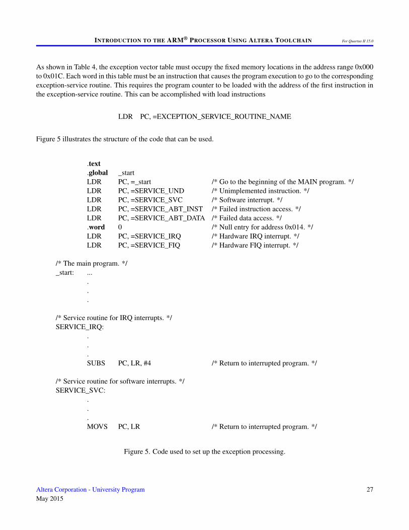
As shown in Table 4, the exception vector table must occupy the fixed memory locations in the address range 0x000to 0x01C. Each word in this table must be an instruction that causes the program execution to go to the correspondingexception-service routine. This requires the program counter to be loaded with the address of the first instruction inthe exception-service routine. This can be accomplished with load instructions
LDR PC, =EXCEPTION_SERVICE_ROUTINE_NAME
Figure 5 illustrates the structure of the code that can be used.
.text
.global _startLDR PC, =_start /* Go to the beginning of the MAIN program. */LDR PC, =SERVICE_UND /* Unimplemented instruction. */LDR PC, =SERVICE_SVC /* Software interrupt. */LDR PC, =SERVICE_ABT_INST /* Failed instruction access. */LDR PC, =SERVICE_ABT_DATA /* Failed data access. */.word 0 /* Null entry for address 0x014. */LDR PC, =SERVICE_IRQ /* Hardware IRQ interrupt. */LDR PC, =SERVICE_FIQ /* Hardware FIQ interrupt. */
/* The main program. */_start: ...
.
.
.
/* Service routine for IRQ interrupts. */SERVICE_IRQ:
.
.
.SUBS PC, LR, #4 /* Return to interrupted program. */
/* Service routine for software interrupts. */SERVICE_SVC:
.
.
.MOVS PC, LR /* Return to interrupted program. */
Figure 5. Code used to set up the exception processing.
Altera Corporation - University ProgramMay 2015
27
INTRODUCTION TO THE ARM® PROCESSOR USING ALTERA TOOLCHAIN For Quartus II 15.0
Observe that 0x000 is inserted in address location 0x014, because this vector location is not allocated to servicing anexception. Observe also that the return from the exception-service routines used as an example is done as explainedin sections 11.2 and 11.2.1.
12 Input/Output Operations
Most I/O devices are accessed by means of their memory-mapped registers. When a program accesses such devices,it is important that each access is made to an actual register. In a processor with a data cache, it is essential to ensurethat the cached data is not used instead of the current values in the I/O device registers. In effect, the data cachehas to be bypassed when reading or writing the registers in I/O devices. The ARM processor does not have separateinstructions for reading and writing the contents of I/O registers. Instead, all I/O devices must have their registersmapped into a memory address region that will not be cached by the processor. This can be accomplished if theprocessor data cache is disabled completely, or if the processor’s memory management unit (MMU) is set up suchthat appropriate regions of memory are designated as non-cacheable. The procedure for setting up the MMU anddata cache is beyond the scope of this document.
Copyright ©1991-2016 Altera Corporation. All rights reserved. Altera, The Programmable Solutions Company, thestylized Altera logo, specific device designations, and all other words and logos that are identified as trademarksand/or service marks are, unless noted otherwise, the trademarks and service marks of Altera Corporation in theU.S. and other countries. All other product or service names are the property of their respective holders. Alteraproducts are protected under numerous U.S. and foreign patents and pending applications, mask work rights, andcopyrights. Altera warrants performance of its semiconductor products to current specifications in accordance withAltera’s standard warranty, but reserves the right to make changes to any products and services at any time withoutnotice. Altera assumes no responsibility or liability arising out of the application or use of any information, product,or service described herein except as expressly agreed to in writing by Altera Corporation. Altera customers areadvised to obtain the latest version of device specifications before relying on any published information and beforeplacing orders for products or services.
This document is being provided on an “as-is” basis and as an accommodation and therefore all warranties, repre-sentations or guarantees of any kind (whether express, implied or statutory) including, without limitation, warrantiesof merchantability, non-infringement, or fitness for a particular purpose, are specifically disclaimed.
28 Altera Corporation - University ProgramMay 2015