Embed Size (px)
Citation preview

FN8944Rev.1.00
Aug 24, 2017
ISL32741EPROFIBUS Compliant 6kV VDE-Reinforced Isolated RS-485 Transceiver
DATASHEET
The ISL32741E is a galvanically isolated, high-speed differential bus transceiver, designed for bidirectional data communication on balanced transmission lines. The device uses Giant Magnetoresistance (GMR) as its isolation technology.
The part is available in a 16 Ld SOICW package with true 8mm creepage distance.
The ISL32741E is PROFIBUS compliant, including the rigorous PROFIBUS differential output voltage specifications.
A unique ceramic/polymer composite barrier provides 6kV reinforced isolation and 44,000 years of barrier life.
The device is compatible with 3V and 5V input supplies, allowing an interface to standard microcontrollers without additional level shifting.
Current limiting and thermal shutdown features protect against output short circuits and bus contention that may cause excessive power dissipation. Receiver inputs are a full fail-safe design, ensuring a logic high R-output if A/B are floating or shorted.
Applications• PROFIBUS-DP and RS-485 networks
• Factory automation
• Building environmental control systems
• Industrial/process control networks
• Equipment covered under IEC 61010-1 Edition 3
Features• 40Mbps data rate
• 6kVRMS isolation/1000VRMS working voltage
• 12.8kV surge immunity
• 3V to 5V power supplies
• 20ns propagation delay
• 5ns pulse skew
• 50kV/µs (typical), 30kV/µs (minimum) common-mode transient immunity
• 15kV ESD protection
• Low EMC footprint
• Thermal shutdown protection
• Temperature Ranges available
• -40°C to +85°C (EIBZ) and -40°C to +125°C (EFBZ)
• Meets or exceeds ANSI RS-485 and ISO 8482:1987(E)
• PROFIBUS compliant
• 0.3” true 8mm 16 Ld SOICW package
• UL 1577 Certification pending
• VDE V 0884-10 certification pending
Related Literature• For a full list of related documents, visit our website
• ISL32741E product page
Figure 1. Typical PROFIBUS Application
ISL32741E
16
12
13
10
9,15
VDD2
B
A
ISODE
GND2
1
4
3
5
6
2, 8
VDD1
R
DE
D
RE
GND1
ISOLATION BARRIER
390R
390R
220R
100n5V
100n
12
13
10
390R
390R
220R
100n3.3V
1M 4.7n 1M4.7n
ISL32741E
16
9,15
VDD2
B
A
ISODE
GND2
1
4
3
5
6
2, 8
VDD1
R
DE
D
RE
GND1
ISOLATION BARRIER
5V
100n
3.3V
FN8944 Rev.1.00 Page 1 of 19Aug 24, 2017

ISL32741E 1. Overview
1. Overview
1.1 Typical Operating Circuit
1.2 Ordering Information
Figure 2. Typical Operating Circuit
Part Number(Notes 1, 2, 3) Part Marking
Temp. Range(°C)
Package(RoHS Compliant) Pkg. Dwg. #
ISL32741EIBZ 32741EIBZ -40 to +85 16 Ld SOICW M16.3A
ISL32741EFBZ 32741EFBZ -40 to +125 16 Ld SOICW M16.3A
ISL32741EVAL1Z Evaluation board
Notes:1. Add “-T” suffix for 1k unit or “-T7A” suffix for 250 unit tape and reel options. Refer to TB347 for details on reel specifications.2. Intersil Pb-free plus anneal products employ special Pb-free material sets; molding compounds/die attach materials and 100%
matte tin plate termination finish, which are RoHS compliant and compatible with both SnPb and Pb-free soldering operations. Intersil Pb-free products are MSL classified at Pb-free peak reflow temperatures that meet or exceed the Pb-free requirements of IPC/JEDEC J STD-020.
3. For Moisture Sensitivity Level (MSL), see the product information page for ISL32741E. For more information on MSL, see TB363.
Table 1. Key Differences Between Family of Parts
Part Number Full/Half DuplexVDD1
(V)VDD2
(V)Data Rate
(Mbps)Isolation Voltage
(kVRMS)
ISL32704E Half 3.0 – 5.5 4.5 – 5.5 4 2.5
ISL32705E Full 3.0 – 5.5 4.5 – 5.5 4 2.5
ISL32740E Half 3.0 – 5.5 4.5 – 5.5 40 2.5
ISL32741E Half 3.0 – 5.5 4.5 – 5.5 40 6
16
12
13
10
9,15
VDD2
B
A
ISODE
GND2
1
4
3
6
5
2, 8
VDD1
R
D
DE
RE
GND1
ISOLATION BARRIER
RFS390R
RFS390R
RT220R
100n
5V100n
ISL32741E
16
12
13
10
9,15
VDD2
B
A
ISODE
GND2
1
4
3
6
5
2, 8
VDD1
R
D
DE
RE
GND1
ISOLATION BARRIER
RFS390R
RFS390R
RT220R
100n
ISL32741E
3.3V 5V 3.3V100n
Z0 = 150R ±10%
FN8944 Rev.1.00 Page 2 of 19Aug 24, 2017

ISL32741E 1. Overview
1.3 Pin Configuration
1.4 Truth Tables
ISL32741E(16 Ld SOICW)
Top View
Transmitting
Inputs Outputs
RE DE D ISODE B A
X 1 1 1 0 1
X 1 0 1 1 0
0 0 X 0 High-Z High-Z
1 0 X 0 High-Z* High-Z*
Receiving
Inputs Output
RE DE A-B RO
0 0 VAB ≥ -0.05V 1
0 0 -0.05V > VAB >-0.2V Undetermined
0 0 VAB ≤ -0.2V 0
0 0 Inputs Open/Shorted 1
1 1 X High-Z
1 0 X High-Z*
Note: *Transceiver shutdown mode
16
15
13
12
14
11
10
9
NC
VDD2
A
NC
B
ISODE
GND2
GND2
1
2
4
3
5
6
8
7
VDD1
R
DE
D
RE
NC
GND1
GND1
FN8944 Rev.1.00 Page 3 of 19Aug 24, 2017

ISL32741E 1. Overview
1.5 Pin Descriptions
Pin Number
Pin Name Function
1 VDD1 Input power supply.
2, 8 GND1 Input power supply ground return. Pin 2 is internally connected to Pin 8.
3 R Receiver output: If A-B ≥-50mV, R is high; If A-B ≤-200mV, R is low; R = High if A and B are unconnected (floating) or shorted, or connected to a terminated bus that is not driven.
4 RE Receiver output enable. R is enabled when RE is low; R is high impedance when RE is high. If the Rx enable function is not required, connect RE directly to GND1.
5 DE Driver output enable. The driver outputs, A and B, are enabled by bringing DE high. They are high impedance when DE is low. If the Tx enable function isn’t required, connect DE to VDD1 through a 1kΩ or greater resistor.
6 D Driver input. A low on D forces output A low and output B high. Similarly, a high on D forces output A high and output B low.
7, 11, 14 NC No internal connection.
9, 15 GND2 Output power supply ground return. Pin 9 is internally connected to Pin 15.
10 ISODE Isolated DE output for use in PROFIBUS applications where the state of the isolated drive enable node needs to be monitored.
12 A ±15kV IEC61000 ESD protected RS-485/RS422 level, noninverting receiver input if DE = 0 and noninverting driver output if DE = 1.
13 B ±15kV IEC61000 ESD protected RS-485/RS422 level, inverting receiver input if DE = 0 and inverting driver output if DE = 1.
16 VDD2 Output power supply.
FN8944 Rev.1.00 Page 4 of 19Aug 24, 2017
ISL32741E 2. Specifications
2. Specifications
2.1 Absolute Maximum Ratings
CAUTION: Do not operate at or near the maximum ratings listed for extended periods of time. Exposure to such conditions may adversely impact product reliability and result in failures not covered by warranty.
2.2 Thermal Information
2.3 Recommended Operation Conditions
Parameter (Note 4) Minimum Maximum Unit
Supply Voltages (Note 7)
VDD1 to GND1 -0.5 +7 V
VDD2 to GND2 7 V
Input Voltages D, DE, RE -0.5 VDD1 + 0.5 V
Input/Output Voltages
A, B -9 +13 V
R -0.5 VDD1 + 1 V
Short-Circuit Duration A, B Continuous V
ESD Rating See “Electrical Specifications” table on page 7
Note:4. Absolute Maximum specifications mean the device will not be damaged if operated under these conditions. It does not
guarantee performance.
Thermal Resistance (Typical) JA (°C/W) JC (°C/W)
16 Ld SOICW Package (Notes 5, 6) 43 20
Notes:5. JA is measured in free air with the component soldered to a double-sided board.6. For JC, the “case temp” location is the center of the package top side.
Parameter Minimum Maximum Unit
Maximum Junction Temperature (Plastic Package) -55 +150 °C
Maximum Storage Temperature Range -55 +150 °C
Maximum Power Dissipation 800 mW
Pb-Free Reflow Profile see TB493
Parameter Minimum Maximum Unit
Supply Voltages
VDD1 3.0 5.5 V
VDD2 4.5 5.5 V
High-Level Digital Input Voltage, VIH
VDD1 = 3.3V 2.4 VDD1 V
VDD1 = 5.0V 3.0 VDD1 V
Low-Level Digital Input Voltage, VIL 0 0.8 V
Differential Input Voltage, VID (Note 8) -7 12 V
FN8944 Rev.1.00 Page 5 of 19Aug 24, 2017
ISL32741E 2. Specifications
2.4 Electrical Specifications
High-Level Output Current (Driver), IOH 60 mA
High-Level Digital Output Current (Receiver), IOH 8 mA
Low-Level Output Current (Driver), IOL -60 mA
Low-Level Digital Output Current (Receiver), IOL -8 mA
Junction Temperature, TJ -40 +110 °C
Ambient Operating Temperature, TA ISL32741EIBZ -40 +85 °C
ISL32741EFBZ -40 +125 °C
Digital Input Signal Rise and Fall Times, tIR, tIF DC Stable
Test conditions: Tmin to Tmax, VDD1 = VDD2 = 4.5V to 5.5V; unless otherwise stated. (Note 7)
Parameter Symbol Test Conditions MinTyp
(Note 11) Max Unit
DC Characteristics
Driver Line Output Voltage (VA, VB) (Note 7)
VO No load - - VDD2 V
Driver Differential Output Voltage (Note 8) VOD1 No load - - VDD2 V
Driver Differential Output Voltage (Note 8) VOD2 RL = 54Ω 2.1 2.8 VDD2 V
Driver Differential Output Voltage(Notes 8, 12)
VOD3 RL = 60Ω 1.9 2.7 - V
Change in Magnitude of Differential Output Voltage (Note 13)
VOD RL = 54Ω or 100Ω - 0.01 0.20 V
Driver Common-Mode Output Voltage VOC RL = 54Ω or 100Ω - - 3 V
Change in Magnitude of Driver Common-Mode Output Voltage (Note 13)
VOC RL = 54Ω or 100Ω - 0.01 0.20 V
Bus Input Current (A, B) (Notes 10, 14) IIN2 DE = 0V VIN = 12V - 220 µA
VIN = -7V -160 µA
High-Level Input Current (DI, DE, RE) IIH VI = 3.5V - - 10 µA
Low-Level Input Current (DI, DE, RE) IIL VI = 0.4V -10 - - µA
Absolute Short-Circuit Output Current IOS DE = VDD1, -7V ≤ VA or VB ≤ 12V - - ±250 mA
Supply Current IDD1 VDD1 = 5V - 4 6 mA
VDD1 = 3.3V - 3 4 mA
Positive-Going Input Threshold Voltage VTH+ -7V ≤ VCM ≤ 12V - - -50 mV
Negative-Going Input Threshold Voltage VTH- -7V ≤ VCM ≤ 12V -200 - - mV
Receiver Input Hysteresis VHYS VCM = 0V - 28 - mV
Differential Bus Input Capacitance CD - 9 12 pF
Receiver Output High Voltage VOH IO = -20µA, VID = -50mV VCC - 0.2 - - V
Receiver Output Low Voltage VOL IO = +20µA, VID = -200mV - - 0.2 V
High impedance Output Current IOZ 0.4V ≤ VO ≤ (VDD2 - 0.5) -1 - 1 µA
Receiver Input Resistance RIN -7V ≤ VCM ≤ 12V 54 80 - kΩ
Supply Current IDD2 DE = VDD1, no load - 5 16 mA
Parameter Minimum Maximum Unit
FN8944 Rev.1.00 Page 6 of 19Aug 24, 2017

ISL32741E 2. Specifications
ESD Performance
RS-485 Bus Pins (A, B) IEC61000-4-2, air-gap discharge to GND2
- ±15 - kV
IEC61000-4-2, contact discharge to GND2
- ±8 - kV
Human Body Model (HBM) discharge to GND2
- ±16.5 - kV
All Pins (R, RE, D, DE) Human Body Model (HBM) discharge to GND1
- ±2 - kV
Switching Characteristics
VDD1 = 5V, VDD2 = 5V
Data Rate DR RL = 54Ω, CL = 50pF 40 - - Mbps
Propagation Delay (Notes 8, 15) tPD VO = -1.5V to 1.5V, CL = 15pF - 20 30 ns
Pulse Skew (Notes 8, 16) tSK (P) VO = -1.5V to 1.5V, CL = 15pF - 1 5 ns
Skew Limit (Note 9) tSK (LIM) RL = 54Ω, CL = 50pF - 2 10 ns
Output Enable Time to High Level tPZH CL = 15pF - 15 30 ns
Output Enable Time to Low Level tPZL CL = 15pF - 15 30 ns
Output Disable Time from High Level tPHZ CL = 15pF - 15 30 ns
Output Disable Time from Low Level tPLZ CL = 15pF - 15 30 ns
Common-Mode Transient Immunity CMTI VCM = 1500 VDC, tTRANSIENT = 25ns 30 50 - kV/µs
VDD1 = 3.3V, VDD2 = 5V
Data Rate DR RL = 54Ω, CL = 50pF 40 - - Mbps
Propagation Delay (Notes 8, 2) tPD VO = -1.5V to 1.5V, CL = 15pF - 25 35 ns
Pulse Skew (Notes 8, 3) tSK (P) VO = -1.5V to 1.5V, CL = 15pF - 2 5 ns
Skew Limit (Note 9) tSK (LIM) RL = 54Ω, CL = 50pF - 4 10 ns
Output Enable Time to High Level tPZH CL = 15pF - 17 30 ns
Output Enable Time to Low Level tPZL CL = 15pF - 17 30 ns
Output Disable Time from High Level tPHZ CL = 15pF - 17 30 ns
Output Disable Time from Low Level tPLZ CL = 15pF - 17 30 ns
Common-Mode Transient Immunity CMTI VCM = 1500 VDC, tTRANSIENT = 25ns 30 50 - kV/µs
Notes: (apply to both driver and receiver sections)7. All voltages on the isolator primary side are with respect to GND1, all line voltages and common-mode voltages on the isolator
secondary or bus side are with respect to GND2. 8. Differential I/O voltage is measured at the noninverting bus Terminal A with respect to the inverting Terminal B.9. Skew limit is the maximum propagation delay difference between any two devices at +25°C.
10. The power-off measurement in ANSI Standard EIA/TIA-422-B applies to disabled outputs only and is not applied to combined inputs and outputs.
11. All typical values are at VDD1, VDD2 = 5V or VDD1 = 3.3V and TA = +25°C.12. -7V < VCM < 12V; 4.5 < VDD < 5.5V.13. VOD and VOC are the changes in magnitude of VOD and VOD respectively, that occur when the input is changed from one
logic state to the other.14. This applies for both power-on and power-off; refer to ANSI standard RS-485 for the exact condition. The EIA/TIA-422 -B limit
does not apply for a combined driver and receiver terminal.15. Includes 10ns read enable time. Maximum propagation delay is 25ns after read assertion.16. Pulse skew is defined as |tPLH - tPHL| of each channel.
Test conditions: Tmin to Tmax, VDD1 = VDD2 = 4.5V to 5.5V; unless otherwise stated. (Note 7) (Continued)
Parameter Symbol Test Conditions MinTyp
(Note 11) Max Unit
FN8944 Rev.1.00 Page 7 of 19Aug 24, 2017

ISL32741E 2. Specifications
2.5 Insulation Specifications
2.6 Magnetic Field Immunity
Parameter Symbol Test Conditions Min Typ Max Unit
Creepage Distance (External) Per IEC 60601 8.03 8.3 - mm
Total Barrier Thickness (Internal) - 13 - µm
Barrier Resistance RIO 500V - >1014 - Ω
Barrier Capacitance CIO f = 1MHz - 7 - pF
Leakage Current 240VRMS, 60Hz - 0.2 - µARMS
Comparative Tracking Index CTI Per IEC 60112 ≥600 - - VRMS
High Voltage Endurance (Maximum Barrier Voltage for Indefinite Life)
VIO At maximum operating temperature 1000 - - VRMS
1500 - - VDC
Barrier Life 100°C, 1000VRMS, 60% CL activation energy
- 44000 - Years
Parameter (Note 17) Symbol Test Conditions Min Typ Max Unit
VDD1 = 5V, VDD2 = 5V
Power Frequency Magnetic Immunity HPF 50Hz/60Hz - 3500 - A/m
Pulse Magnetic Field Immunity HPM tP = 8µs - 4500 - A/m
Damped Oscillatory Magnetic Field HOSC 0.1Hz to 1MHz - 4500 - A/m
Cross-Axis Immunity Multiplier (Note 18) KX - 2.5 - A/m
VDD1 = 3.3V, VDD2 = 5V
Power Frequency Magnetic Immunity HPF 50Hz/60Hz - 1500 - A/m
Pulse Magnetic Field Immunity HPM tP = 8µs - 2000 - A/m
Damped Oscillatory Magnetic Field HOSC 0.1Hz to1MHz - 2000 - A/m
Cross-Axis Immunity Multiplier (Note 18) KX - 2.5 - A/m
Notes:17. The relevant test and measurement methods are given in the “Electromagnetic Compatibility” on page 10.18. External magnetic field immunity is improved by this factor if the field direction is “end-to-end” rather than “pin-to-pin”
(See “Electromagnetic Compatibility” on page 10).
FN8944 Rev.1.00 Page 8 of 19Aug 24, 2017

ISL32741E 3. Safety and Approvals
3. Safety and Approvals
3.1 VDE V 0884-11 (Certification Pending)Standard Isolation Grade; File Number: Certifications pending
• Working voltage (VIORM) 1000VRMS (1415VPK); Reinforced insulation, Pollution degree 2
• Isolation voltage (VISO) 6000VRMS
• Surge Immunity (VIOSM) 12.8kVPK
• Surge rating 8kV
• Transient overvoltage (VIOTM) 6000VPK
• Each part tested at 2387VPK for 1s, 5pC partial discharge limit
• Samples tested at 6000VPK for 60s, then 2122VPK for 10s with 5pC partial discharge limit
3.2 UL 1577 Reinforced Isolation Grade; Recognition Pending
• 6kV rating
• Each part tested at 7.2kVRMS (10.2kVPK) for 1s
• Each lot samples tested at 6000VRMS (8485VPK) for 60s
Symbol Safety-Limiting Values Value Unit
TS Safety Rating Ambient Temperature +180 °C
PS Safety Rating Power (+180°C) 270 mW
IS Supply Current Safety Rating (total of supplies) 54 mA
FN8944 Rev.1.00 Page 9 of 19Aug 24, 2017
ISL32741E 4. Electromagnetic Compatibility
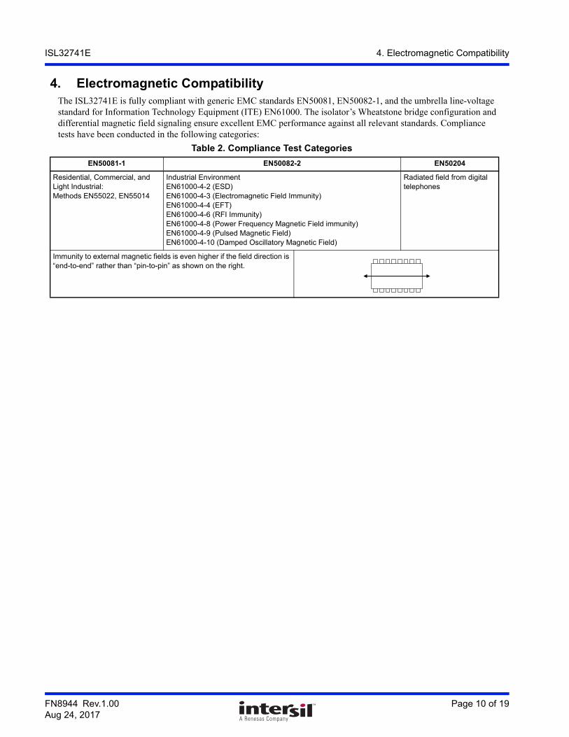
4. Electromagnetic CompatibilityThe ISL32741E is fully compliant with generic EMC standards EN50081, EN50082-1, and the umbrella line-voltage standard for Information Technology Equipment (ITE) EN61000. The isolator’s Wheatstone bridge configuration and differential magnetic field signaling ensure excellent EMC performance against all relevant standards. Compliance tests have been conducted in the following categories:
Table 2. Compliance Test Categories
EN50081-1 EN50082-2 EN50204
Residential, Commercial, and Light Industrial:Methods EN55022, EN55014
Industrial EnvironmentEN61000-4-2 (ESD)EN61000-4-3 (Electromagnetic Field Immunity)EN61000-4-4 (EFT)EN61000-4-6 (RFI Immunity)EN61000-4-8 (Power Frequency Magnetic Field immunity)EN61000-4-9 (Pulsed Magnetic Field)EN61000-4-10 (Damped Oscillatory Magnetic Field)
Radiated field from digital telephones
Immunity to external magnetic fields is even higher if the field direction is “end-to-end” rather than “pin-to-pin” as shown on the right.
FN8944 Rev.1.00 Page 10 of 19Aug 24, 2017

ISL32741E 5. Application Information
5. Application InformationThe ISL32741E is a 6kV reinforced isolated PROFIBUS transceiver specifically designed for PROFIBUS-DP applications.
5.1 PROFIBUSThis transceiver uses a differential input receiver for maximum noise immunity and common-mode rejection. PROFIBUS (Process Field Bus) is specified in IEC61158 as a standard for field bus communication in automation technology. Two versions of PROFIBUS exist: PROFIBUS - PA for Process Automation and PROFIBUS-DP for Decentralized Peripherals. The most commonly used, PROFIBUS-DP, is a protocol for deterministic communication between PROFIBUS masters and their remote I/O slaves.
While the physical layer of PROFIBUS-DP is based on RS-485 with its differential signaling scheme, significant differences between the two physical layers exist with regard to cable type, bus termination, and minimum bus voltage, to name just a few parameters.
5.2 Galvanic IsolationTo enable PROFIBUS transceivers operating over a wider common-mode voltage range than specified in RS-485 (7V to +12V), modern transceiver designs incorporate galvanic digital isolators with the transceiver circuitry. Here the ISL32741E uses a Giant Magnetoresistance (GMR) isolation. Figure 3 shows the principle operation of a single channel GMR isolator.
Figure 3. Single Channel GMR Isolator
The input signal is buffered and drives a primary coil, which creates a magnetic field that changes the resistance of the GMR resistors 1 to 4. GMR1 to GMR4 form a Wheatstone bridge to create a bridge output voltage that reacts only to magnetic field changes from the primary coil. Large external magnetic fields however, are treated as common-mode fields, and are therefore suppressed by the bridge configuration. The bridge output is fed into a comparator whose output signal is identical in phase and shape to the input signal.
Table 3. Main Differences Between RS-485 and PROFIBUS-DP
Parameter RS-485 PROFIBUS-DP
Cable Type Unshielded twisted pair Shielded twisted pair
Characteristic Impedance 120Ω 150Ω
Minimum Driver Output Voltage 1.5V 2.1V
Transceiver Input Capacitance 10 to 15pF 10pF
External Fail-Safe Biasing Customer configurable(none, at single or both cable ends)
Always at both cable ends
Resistor Values Customer configurable Fixed
IN
VDD2
GND2
OUT
EXTERNAL B-FIELD
INTERNALB-FIELD GMR2
GMR4GMR3
GMR1
FN8944 Rev.1.00 Page 11 of 19Aug 24, 2017

ISL32741E 5. Application Information
5.3 GMR Resistor in DetailFigure 4 shows a GMR resistor consisting of ferromagnetic alloy layers B1 and B2 sandwiched around an ultra thin, nonmagnetic conducting middle layer A, typically copper. The GMR structure is designed so that in the absence of a magnetic field, the magnetic moments in B1 and B2 face opposite directions, thus causing heavy electron scattering across layer A, which increases its resistance for current C drastically. When a magnetic field D is applied, the magnetic moments in B1 and B2 are aligned and electron scattering is reduced. This lowers the resistance of layer A and current C increases.
Figure 4. Multilayer GMR Resistor
5.4 Low EmissionsBecause GMR isolators do not use fancy encoding schemes, such as RF carriers or high-frequency clocks, and do not include power transfer coils or transformers, their radiated emission spectrum is practically undetectable.
Figure 5. Undetectable Emissions of GMR Isolators
5.5 Low EMI SusceptibilityBecause GMR isolators have no pulse trains or carriers to interfere with, they also have very low EMI susceptibility.
For the list of compliance tests conducted on GMR isolators, refer to “Electromagnetic Compatibility” on page 10.
5.6 Receiver (Rx) FeaturesThis transceiver uses a differential input receiver for maximum noise immunity and common-mode rejection. Input sensitivity is ±200mV, as required by the RS-422 and RS-485 specifications. Receiver inputs function with common-mode voltages as great as 7V outside the power supplies (for example, +12V and -7V), making them ideal for long networks, or industrial environments, where induced voltages are a realistic concern.
The receiver input resistance of 54kΩ surpasses the RS-422 specification of 4kΩ and is about five times the RS-485 “Unit Load” (UL) requirement of 12kΩ minimum. Thus, the ISL32741E is known as a “one-fifth UL” transceiver, and there can be up to 160 devices on the RS-485 bus while still complying with the RS-485 loading specification.
B1
A
B2
C
B1
A
B2
C C
D
APPLIED MAGNETIC FIELD
HIGH RESISTANCE
LOW RESISTANCE
C
FCC-B < 1GHz 3m
EN55022 < 1GHz 3m
LABORATORY NOISE FLOOR
QP-MEASUREMENTS
10MHz 100MHz 1GHz
60
50
40
30
20
10
0
AM
PL
ITU
DE
(d
Bµ
V/m
)
FN8944 Rev.1.00 Page 12 of 19Aug 24, 2017
ISL32741E 5. Application Information
The receiver is a “full fail-safe” version that ensures a high-level receiver output if the receiver inputs are unconnected (floating), shorted together, or connected to a terminated bus with all the transmitters disabled (terminated/undriven).
Rx outputs deliver large low state currents (typically >30mA) at VOL = 1V.
Receivers easily meet the 40Mbps data rate supported by the driver, and the receiver output is tri-statable using the active low RE input.
5.7 Driver (Tx) FeaturesThe RS-485/RS-422 driver is a differential output device that delivers at least 2.1V across a 54Ω load (RS-485/PROFIBUS), and at least 2.6V across a 100Ω load (RS-422) even with VCC = 4.5V. The drivers feature low propagation delay skew to maximize bit width and to minimize EMI.
Outputs of the drivers are not slew rate limited, so faster output transition times allow data rates of at least 40Mbps. Driver outputs are tri-statable through the active high DE input.
5.7.1 High VOD Improves Noise Immunity and FlexibilityThe ISL32741E driver design delivers larger differential output voltages (VOD) than the RS-485 standard requires, or than most RS-485 transmitters can deliver. The minimum ±2.1V VOD ensures at least ±600mV more noise immunity than networks built using standard 1.5V VOD transmitters.
Another advantage of the large VOD is the ability to drive more than two bus terminations, which allows for using the ISL32741E in “star” and other multi-terminated, “nonstandard” network topologies.
5.8 Built-In Driver Overload ProtectionAs stated previously, the RS-485 specification requires that drivers survive worst case bus contentions undamaged. These transmitters meet this requirement through driver output short-circuit current limits, and on-chip thermal shutdown circuitry.
The driver output stages incorporate short-circuit current limiting circuitry, which ensures that the output current never exceeds the RS-485 specification, even at the common-mode voltage range extremes. In the event of a major short-circuit condition, the device also includes a thermal shutdown feature that disables the drivers whenever the die temperature becomes excessive. This eliminates the power dissipation, allowing the die to cool. The drivers automatically re-enable after the die temperature drops about 15°C. If the contention persists, the thermal shutdown/re-enable cycle repeats until the fault is cleared. Receivers stay operational during thermal shutdown.
5.9 Dynamic Power ConsumptionThe isolator within the ISL32741E achieves its low power consumption from the way it transmits data across the barrier. By detecting the edge transitions of the input logic signal and converting these to narrow current pulses, a magnetic field is created around the GMR Wheatstone bridge. Depending on the direction of the magnetic field, the bridge causes the output comparator to switch following the input signal. Because the current pulses are narrow, about 2.5ns, the power consumption is independent of the mark-to-space ratio and solely depends on frequency.
Table 4. Supply Current Increase with Data Rate
Data Rate(Mbps)
IDD1 (mA)
IDD2 (mA)
1 0.15 0.15
10 1.5 1.5
20 3 3
40 6 6
FN8944 Rev.1.00 Page 13 of 19Aug 24, 2017

ISL32741E 5. Application Information
5.10 Power Supply DecouplingBoth supplies, VDD1 and VDD2, must be bypassed with 100nF ceramic capacitors. These should be placed as close as possible to the supply pins for proper operation.
5.11 DC CorrectnessThe ISL32741E incorporates a patented refresh circuit to maintain the correct output state with respect to data input. At power-up, the bus outputs follow the “Truth Tables” on page 3. The DE input should be held low during power-up to prevent false drive data pulses on the bus.
5.12 Data Rate, Cables, and Terminations Twisted pair is the cable of choice for RS-485, RS-422, and PROFIBUS networks. Twisted pair cables tend to pick up noise and other electromagnetically induced voltages as common-mode signals, which are effectively rejected by the differential receivers in these ICs.
According to guidelines in the RS-422 and PROFIBUS specifications, networks operating at data rates in excess of 3Mbps should be limited to cable lengths of 100m (328 ft) or less and the PROFIBUS specification recommends that the more expensive “Type A” (22AWG) cable be used. The ISL32741E’s large differential output swing, fast transition times, and high drive-current output stages allow operation even at 40Mbps over standard “CAT 5” cables in excess of 100m (328 ft).
The ISL324741E can also be used at slower data rates over longer cables, but there are some limitations. The Rx is optimized for high-speed operation, so its output may glitch if the Rx input differential transition times are too slow. Keeping the transition times below 500ns, (which equates to the Tx driving a 1000’ (305m) CAT 5 cable) yields excellent performance across the full operating temperature range.
To minimize reflections, proper termination is imperative when using this high data rate transceiver. In point-to-point, or point-to-multipoint (single driver on bus) networks, the main cable should be terminated in its characteristic impedance (typically 100Ω for “CAT 5”, 120Ω for RS-485, and 150Ω for “Type A”) at the end farthest from the driver. In multireceiver applications, stubs connecting receivers to the main cable should be kept as short as possible. Multipoint (multidriver) systems require that the main cable be terminated in its characteristic impedance at both ends. Stubs connecting transceivers to the main cable should be kept as short as possible.
PROFIBUS specifies line termination with fail-safe biasing networks of fixed resistor values at both cable ends.
Figure 6. Line Termination for PROFIBUS-DP
For isolated data links meeting the requirements of EIA-485, the resistor values for the fail-safe biasing network can be calculated using (EQ. 1) through (EQ. 4).
For data links longer than 100m (330ft) apply fail-safe biasing at both cable ends to compensate for the attenuation of the bus fail-safe voltage caused by the voltage divider action of the cable’s DC resistance and the remote fail-safe biasing network. Use (EQ. 1) to calculate the bias resistors, RB, and (EQ. 2) to determine the termination resistors, RT.
390R RB
220R RT
390R RB
VS VS
390R
220R
390R
RB
RT
RB
(EQ. 1) RB
VSVAB-----------
Z02
------
FN8944 Rev.1.00 Page 14 of 19Aug 24, 2017

ISL32741E 5. Application Information
where:
• RB is the value of the biasing resistors.
• RT is the value of the termination resistors.
• VS is the minimum transceiver supply voltage.
• VAB is the minimum bus voltage during bus idling.
• Z0 is the characteristic cable impedance of 120Ω.
Figure 7. Dual Fail-Safe Biasing for Long Data Links
For data links shorter than 100m, use a single fail-safe biasing network. Match the termination resistor value at the cable end without fail-safe biasing with the characteristic cable impedance: RT1 = Z0. Then calculate RB using (EQ. 3) and RT2 using (EQ. 4).
Figure 8. Single Fail-Safe Biasing for Short Data Links
Note, the resistor values in Figures 7 and 8 have been calculated for VS = 4.5V, VAB = 0.25V, and Z0 = 120Ω.
(EQ. 2) RT
2RB Z0
2RB Z0–------------------------=
RB
RT
RB
VS1
RB
RT
RB
VS2
GND1 GND2
1.09k
1.09k
127R
1.09k
1.09k
127R
(EQ. 3) RB
VSVAB-----------
Z04
------
(EQ. 4) RT2
2RB Z0
2RB Z0–------------------------=
120R
RB
RT2
RB
VS
RT1
542R
542R
135R
FN8944 Rev.1.00 Page 15 of 19Aug 24, 2017
ISL32741E 5. Application Information
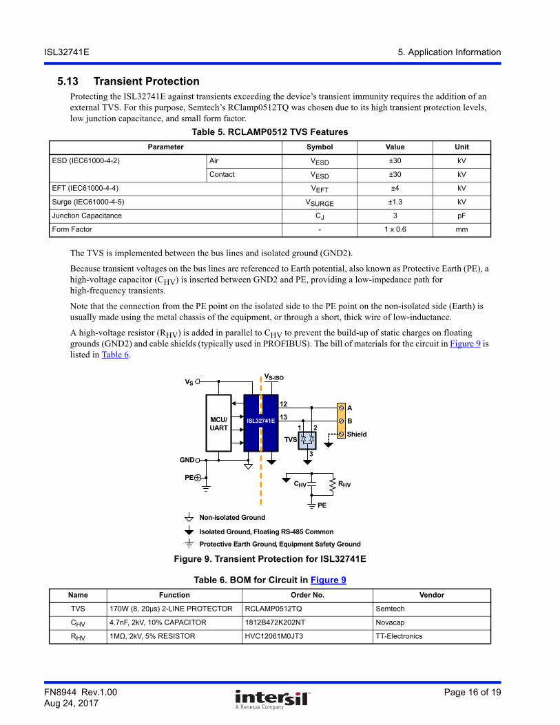
5.13 Transient Protection Protecting the ISL32741E against transients exceeding the device’s transient immunity requires the addition of an external TVS. For this purpose, Semtech’s RClamp0512TQ was chosen due to its high transient protection levels, low junction capacitance, and small form factor.
The TVS is implemented between the bus lines and isolated ground (GND2).
Because transient voltages on the bus lines are referenced to Earth potential, also known as Protective Earth (PE), a high-voltage capacitor (CHV) is inserted between GND2 and PE, providing a low-impedance path for high-frequency transients.
Note that the connection from the PE point on the isolated side to the PE point on the non-isolated side (Earth) is usually made using the metal chassis of the equipment, or through a short, thick wire of low-inductance.
A high-voltage resistor (RHV) is added in parallel to CHV to prevent the build-up of static charges on floating grounds (GND2) and cable shields (typically used in PROFIBUS). The bill of materials for the circuit in Figure 9 is listed in Table 6.
Figure 9. Transient Protection for ISL32741E
Table 5. RCLAMP0512 TVS Features
Parameter Symbol Value Unit
ESD (IEC61000-4-2) Air VESD ±30 kV
Contact VESD ±30 kV
EFT (IEC61000-4-4) VEFT ±4 kV
Surge (IEC61000-4-5) VSURGE ±1.3 kV
Junction Capacitance CJ 3 pF
Form Factor - 1 x 0.6 mm
Table 6. BOM for Circuit in Figure 9
Name Function Order No. Vendor
TVS 170W (8, 20µs) 2-LINE PROTECTOR RCLAMP0512TQ Semtech
CHV 4.7nF, 2kV, 10% CAPACITOR 1812B472K202NT Novacap
RHV 1MΩ, 2kV, 5% RESISTOR HVC12061M0JT3 TT-Electronics
MCU/UART
VS-ISO
13
12
VS
GND
PERHVCHV
B
A
ShieldTVS
ISL32741E
PE
1 2
3
Protective Earth Ground, Equipment Safety Ground
Isolated Ground, Floating RS-485 Common
Non-isolated Ground
FN8944 Rev.1.00 Page 16 of 19Aug 24, 2017

ISL32741E 6. Revision History
6. Revision History
Rev. Date Description
1.00 Aug 24, 2017 Updated Table 1 on page 2.Updated receiving truth table.
0.00 Jun 28, 2017 Initial release
FN8944 Rev.1.00 Page 17 of 19Aug 24, 2017

ISL32741E 7. Package Outline Drawing
.
7. Package Outline DrawingM16.3A16 LEAD WIDE BODY SMALL OUTLINE PLASTIC PACKAGE (SOICW)Rev 1, 6/17
END VIEW
16
1 8
9
PIN #1I.D. MARK
SIDE VIEW
TYPICAL RECOMMENDED LAND PATTERN
0.3 MAX0.1 MIN
DETAIL X
GAUGE
0.05
TOP VIEW
SEATING
PLANE
C
H
SEE DETAIL "X"
0.30.5
1.241.30
0.851.10
0.20.3
0.180.25
0.30.5
0.40 0° TO 8°
0.25
1.30
2.342.67
0.10.3
(0.51)(1.27)
0.10 C 0.1 C BM A
1 3
2 3
5
10.0810.49
10.0010.64
7.427.59
6.607.11
PLANE
2.02.5
(1.7)
(9.75)
NOTES:
19. Dimension does not include mold flash, protrusions, or gate burrs. Mold flash, protrusions, or gate burrs shall not exceed 0.15 per side
20. Dimension does not include interlead flash or protrusion. Interlead flash or protrusion shall not exceed 0.25 per side.
21. Dimensions are measured at datum plane H.
22. Dimensioning and tolerancing per ASME Y14.5M-1994.
23. Dimension does not include dambar protrusion.
24. Dimension in ( ) are for reference only.
25. Pin spacing is a BASIC dimension; tolerances do not accumulate.
26. Dimensions are in mm.
For the most recent package outline drawing, see M16.3A.
FN8944 Rev.1.00 Page 18 of 19Aug 24, 2017

ISL32741E 8. About Intersil
Intersil products are manufactured, assembled and tested utilizing ISO9001 quality systems as notedin the quality certifications found at www.intersil.com/en/support/qualandreliability.html
Intersil products are sold by description only. Intersil may modify the circuit design and/or specifications of products at any time without notice, provided that such modification does not, in Intersil's sole judgment, affect the form, fit or function of the product. Accordingly, the reader is cautioned to verify that datasheets are current before placing orders. Information furnished by Intersil is believed to be accurate and reliable. However, no responsibility is assumed by Intersil or its subsidiaries for its use; nor for any infringements of patents or other rights of third parties which may result from its use. No license is granted by implication or otherwise under any patent or patent rights of Intersil or its subsidiaries.
For information regarding Intersil Corporation and its products, see www.intersil.com
For additional products, see www.intersil.com/en/products.html
© Copyright Intersil Americas LLC 2017. All Rights Reserved.All trademarks and registered trademarks are the property of their respective owners.
8. About IntersilIntersil Corporation is a leading provider of innovative power management and precision analog solutions. The company's products address some of the largest markets within the industrial and infrastructure, mobile computing and high-end consumer markets.
For the most updated datasheet, application notes, related documentation and related parts, please see the respective product information page found at www.intersil.com.
For a listing of definitions and abbreviations of common terms used in our documents, visit: www.intersil.com/glossary.
You can report errors or suggestions for improving this datasheet by visiting www.intersil.com/ask.
Reliability reports are also available from our website at www.intersil.com/support.
FN8944 Rev.1.00 Page 19 of 19Aug 24, 2017