Embed Size (px)
Citation preview

Freescale Semiconductor Document Number: DRM149
Design Reference Manual Rev. 0, 04/2014
© Freescale Semiconductor, Inc., 2014. All rights reserved.
_______________________________________________________________________
Kinetis-M Two-Phase Power Meter
Reference Design by: Luděk Šlosarčík
1 Introduction
The electro-mechanical power meter has been
gradually replaced by the electronic meter.
Modern electronic meters have a number of
advantages over their electro-mechanical
predecessors. Their mechanical construction is
more cost-effective due to the fact that there are
no moving parts. In addition, electronic meters
have one percent accuracy or better in the
typical dynamic range of power measurement of
1000:1, whereas electro-mechanical meters have
two percent accuracy in the dynamic range of
80:1. The higher the accuracy and dynamic
range of the measurement, the more precise the
energy bills.
This design reference manual describes a
solution for a two-phase electronic power meter
based on the MKM34Z128CLL5
microcontroller. This microcontroller is part of
the Freescale Kinetis-M series of MCUs. The
Kinetis-M series microcontrollers address
accuracy needs by providing a high-
performance analog front-end (24-bit AFE)
combined with an embedded Programmable
Gain Amplifier (PGA). Besides high-
performance analog peripherals, these new
devices integrate memories, input-output ports,
digital blocks, and a variety of communication
options. Moreover, the ARM Cortex-M0+ core,
with support for 32-bit math, enables fast
execution of metering algorithms.
Contents 1 Introduction ...................................................... 1
1.1 Specification ...................................................... 2 2 MKM34Z128 microcontroller series ............... 4 3 Basic theory ..................................................... 5
3.1 Active energy ..................................................... 5 3.2 Reactive energy ................................................. 5 3.3 Active power ...................................................... 6 3.4 Reactive power .................................................. 6 3.5 RMS current and voltage .................................. 6 3.6 Apparent Power ................................................. 7 3.7 Power factor ...................................................... 7
4 Hardware design .............................................. 7 4.1 Power supply ..................................................... 8 4.2 Digital circuits ................................................... 9 4.3 Optional communication interfaces .............. 12 4.4 Analog circuits ................................................ 15
5 Software design ............................................. 17 5.1 Block diagram ................................................. 17 5.2 Software tasks ................................................. 18 5.3 Performance .................................................... 24
6 Application set-up .......................................... 24 7 FreeMASTER visualization ........................... 27 8 HAN/NAN visualization .................................. 31 9 Accuracy and performance .......................... 31
9.1 Room temperature accuracy testing .................. 32 9.2 Extended temperature accuracy testing ............ 33
10 Summary ......................................................... 34 11 References ...................................................... 35 12 Revision history ............................................. 37

Kinetis-M Two-Phase Power Meter Reference Design, Rev. 0, 04/2014
2 Freescale Semiconductor
The two-phase power meter reference design is intended for the measurement and registration of active
and reactive energies in two-phase networks. It is targeted specifically at the American and Japanese
regions. Depending on the target region, it is pre-certified according to different standards; the ANSI
C12.20-2002, accuracy classes 0.2 and 0.5 for the U.S., and the international standard IEC 62053-22,
accuracy classes 0.2S and 0.5S for Japan.
The integrated Switched-Mode Power Supply (SMPS) enables an efficient operation of the power meter
electronics and provides enough power for optional modules, such as non-volatile memories (NVM) for
data logging and firmware storage, two low-power digital 3-axis Xtrinsic sensors for electronic tamper
detection, and a Radio Frequency (RF) communication module for Automatic Meter Reading (AMR)
and remote monitoring. The power meter electronics are backed up by a 3.6 V Li-SOCI2 battery when
disconnected from the mains. The meter has no mechanical tampers, only electronic ones. One tamper
event may be generated by an ultra-low-power 3-axis Xtrinsic tilt sensor. With the tilt sensor populated,
the meter electronics are powered when the coordinates of the installed meter unexpectedly change. The
tilt sensor in the meter not only prevents physical tampering, but can also activate the power meter
electronics to disconnect a house from the mains in the case of an earthquake. The second tamper event
may be generated by a low-power 3-axis Xtrinsic magnetometer, which can detect a magnetic field
caused by an external strong magnet. This magnetic field may negatively affect the current transformers
used inside the meter.
The power meter reference design is prepared for use in real applications, as suggested by its
implementation of a Human Machine Interface (HMI) and communication interfaces for remote data
collection.
1.1 Specification
As previously indicated, the Kinetis-M two-phase power meter reference design is ready for use in a real
application. More precisely, its metrology portion has undergone thorough laboratory testing using the
test equipment ELMA8303 [1]. Thanks to intensive testing, an accurate 24-bit AFE, and continual
algorithm improvements, the two-phase power meter calculates active and reactive energies more
accurately and over a higher dynamic range than required by common standards. All information,
including accuracies, operating conditions, and optional features, are summarized in the two following
tables according to the target version (U.S. or Japan):
Table 1-1. Kinetis-M two-phase power meter specification (U.S. version)
Type of meter Two-phase residential active and reactive energy meter
Type of measurement 4-quadrant
Metering algorithm Fast Fourier Transform or Filter based
Accuracy ANSI C12.20-2002 Class 0.2 (for active and reactive energy)
Nominal Voltage 120 VAC 20%
Current Class CL200
Test Current 30 A
Staring Current 50 mA
Nominal Frequency 60 Hz 6
List of impulse numbers for FFT-based algorithm (imp/kWh, imp/kVArh)
500, 1000, 2000, 50002), 10000
2), 20000
2), 50000
2), 100000
2)
List of impulse numbers for Filter-based algorithm (imp/kWh, imp/kVArh)
100, 200, 500, 1000, 2000, 5000, 10000, 20000, 500002), 100000
2),
2000002), 500000
2), 1000000
2)

Kinetis-M Two-Phase Power Meter Reference Design, Rev. 0, 04/2014
Freescale Semiconductor 3
Default Watt-hour (VAr-hour) constant Kh=0.2 (Filter-based algorithm) or Kh=0.5 (FFT-based algorithm)
Functionality V, A, kW, VAr, VA, kWh (import/export), kVArh (import/export), Hz, power factor, time, date, serial number and SW version
Voltage sensor Voltage divider (VTR 2000:1)
Current sensor Current Transformer (CTR 2000:1), type CHEM 9912192
Energy output pulse interface Two super bright red LEDs (active and reactive energy)
Optoisolated pulse output (optional only) Optocoupler (active or reactive energy)
User interface (HMI) 160-segment LCD, one user red LED
Electronic tamper detection 3-axis magnetometer MAG3110, 3-axis accelerometer MMA8491Q
Infrared interface1) According to ANSI C12.18-2006
Isolated RS232 serial interface (optional only) 19200 Bd, 8 data bits, 1 stop bit, no parity
RF interface (the 1st option)
MC1322x-IPB radio module based on 2.4GHz IEEE 802.15.4
RF interface (the 2nd
option) HAN/NAN radio modules based on 900MHz RF Mesh IEEE 802.15.4g/e and 6loWPAN/IPv6 connectivity
Internal battery (for RTC) 1/2AA, 3.6 V Lithium-Thionyl Chloride (Li-SOCI2) 1.2 Ah
Service type Form 12S
Enclosure According to ANSI C12.10-2004
Power consumption @3.3V and 22°C:
Normal mode (powered from mains)
Standby mode (powered from battery)
Power-down mode (powered from battery)
16.0 mA 3) (measurement mode)
192 A (transition from normal to power-down, duration only 2.5 seconds)
2.6 A 4) (MCU only)
Table 1-2. Kinetis-M two-phase power meter specification (Japan version)
Type of meter Two-phase residential active and reactive energy meter
Type of measurement 4-quadrant
Metering algorithm Fast Fourier Transform or Filter based
Accuracy Class 0.5S, IEC 62053-22, IEC 62052-11 (for active and reactive energy)
Nominal Voltage 100 VAC 20%
Maximum Current 60 A
Nominal Current 5 A
Staring Current 20 mA
Nominal Frequency 50 Hz 8
List of impulse numbers (FFT-based algorithm) (imp/kWh, imp/kVArh)
500, 1000, 2000, 5000, 10000, 200002), 50000
2), 100000
2)
List of impulse numbers (Filter-based algorithm) (imp/kWh, imp/kVArh)
100, 200, 500, 1000, 2000, 5000, 10000, 20000, 500002), 100000
2),
2000002), 500000
2), 1000000
2)
Default Watt-hour (VAr-hour) impulse number 50000 (Filter based algorithm) or 10000 (FFT based algorithm)
Functionality V, A, kW, VAr, VA, kWh (import/export), kVArh (import/export), Hz, power factor, time, date, serial number and SW version
Voltage sensor Voltage divider (VTR 2000:1)
Current sensor Current Transformer (CTR 2000:1), type CHEM 9912192
Energy output pulse interface Two super bright red LEDs (active and reactive energy)
Optoisolated pulse output (optional only) Optocoupler (active or reactive energy)
User interface (HMI) 160-segment LCD, one user red LED
Electronic tamper detection 3-axis magnetometer MAG3110, 3-axis accelerometer MMA8491Q
Infrared interface1) According to IEC1107
Isolated RS232 serial interface (optional only) 19200 Bd, 8 data bits, 1 stop bit, no parity
Kinetis-M Two-Phase Power Meter Reference Design, Rev. 0, 04/2014
4 Freescale Semiconductor
Internal battery (for RTC) 1/2AA, 3.6 V Lithium-Thionyl Chloride (Li-SOCI2) 1.2 Ah
Enclosure According to ANSI C12.10-2004
Power consumption @3.3V and 22°C:
Normal mode (powered from mains)
Standby mode (powered from battery)
Power-down mode (powered from battery)
16.0 mA 3) (measurement mode)
192 A (transition from normal to power-down, duration only 2.5 seconds)
2.6 A 4) (MCU only)
1) This functionality is not implemented in the current SW (Rev. 2.0.0.2). 2) These impulse numbers are applicable only for low current measurement 3) Valid for CORECLK=47.972352 MHz and without any RF communication module 4) Magnetometer, accelerometer, EEPROM and IR interface are switched off (VAUX is not applied)
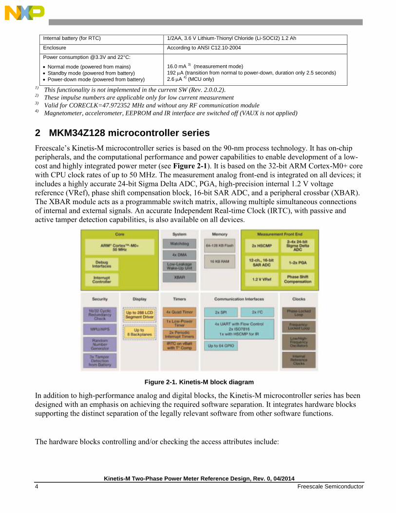
2 MKM34Z128 microcontroller series
Freescale‟s Kinetis-M microcontroller series is based on the 90-nm process technology. It has on-chip
peripherals, and the computational performance and power capabilities to enable development of a low-
cost and highly integrated power meter (see Figure 2-1). It is based on the 32-bit ARM Cortex-M0+ core
with CPU clock rates of up to 50 MHz. The measurement analog front-end is integrated on all devices; it
includes a highly accurate 24-bit Sigma Delta ADC, PGA, high-precision internal 1.2 V voltage
reference (VRef), phase shift compensation block, 16-bit SAR ADC, and a peripheral crossbar (XBAR).
The XBAR module acts as a programmable switch matrix, allowing multiple simultaneous connections
of internal and external signals. An accurate Independent Real-time Clock (IRTC), with passive and
active tamper detection capabilities, is also available on all devices.
Figure 2-1. Kinetis-M block diagram
In addition to high-performance analog and digital blocks, the Kinetis-M microcontroller series has been
designed with an emphasis on achieving the required software separation. It integrates hardware blocks
supporting the distinct separation of the legally relevant software from other software functions.
The hardware blocks controlling and/or checking the access attributes include:

Kinetis-M Two-Phase Power Meter Reference Design, Rev. 0, 04/2014
Freescale Semiconductor 5
ARM Cortex-M0+ Core
DMA Controller Module
Miscellaneous Control Module
Memory Protection Unit
Peripheral Bridge
General Purpose Input-Output Module
The Kinetis-M devices remain first and foremost highly capable and fully programmable
microcontrollers with application software driving the differentiation of the product. Currently, the
necessary peripheral software drivers, metering algorithms, communication protocols, and a vast number
of complementary software routines are available directly from semiconductor vendors or third parties.
Because Kinetis-M microcontrollers integrate a high-performance analog front-end, communication
peripherals, hardware blocks for software separation, and are capable of executing a variety of ARM
Cortex-M0+ compatible software, they are ideal components for development of residential, commercial
and light industrial electronic power meter applications.
3 Basic theory
The critical task for a digital processing engine or a microcontroller in an electricity metering application
is the accurate computation of the active energy, reactive energy, active power, reactive power, apparent
power, RMS voltage, and RMS current. The active and reactive energies are sometimes referred to as the
billing quantities. The remaining quantities are calculated for informative purposes, and they are referred
to as non-billing. Further follows a description of the billing and non-billing metering quantities and
calculation formulas.
3.1 Active energy
The active energy represents the electrical energy produced, flowing or supplied by an electric circuit
during a time interval. The active energy is measured in the unit of watt hours (Wh). The active energy in
a typical one-phase power meter application is computed as an infinite integral of the unbiased
instantaneous phase voltage u(t) and phase current i(t) waveforms.
Eq. 3-1
NOTE
The total active energy in a typical two-phase power meter application is
computed as a sum of two individual active energies.
3.2 Reactive energy
The reactive energy is given by the integral, with respect to time, of the product of voltage and current
and the sine of the phase angle between them. The reactive energy is measured in the unit of volt-
ampere-reactive hours (VARh). The reactive energy in a typical one-phase power meter is computed as
an infinite integral of the unbiased instantaneous shifted phase voltage u(t-90°) and phase current i(t)
waveforms.

Kinetis-M Two-Phase Power Meter Reference Design, Rev. 0, 04/2014
6 Freescale Semiconductor
Eq. 3-2
NOTE
The total reactive energy in a typical two-phase power meter application
is computed as a sum of two individual reactive energies.
3.3 Active power
The active power (P) is measured in watts (W) and is expressed as the product of the voltage and the in-
phase component of the alternating current. In fact, the average power of any whole number of cycles is
the same as the average power value of just one cycle. So, we can easily find the average power of a very
long-duration periodic waveform simply by calculating the average value of one complete cycle with
period T.
Eq. 3-3
3.4 Reactive power
The reactive power (Q) is measured in units of volt-amperes-reactive (VAR) and is the product of the
voltage and current and the sine of the phase angle between them. The reactive power is calculated in the
same manner as active power, but, in reactive power, the voltage input waveform is 90 degrees shifted
with respect to the current input waveform.
Eq. 3-4
3.5 RMS current and voltage
The Root Mean Square (RMS) is a fundamental measurement of the magnitude of an alternating signal.
In mathematics, the RMS is known as the standard deviation, which is a statistical measure of the
magnitude of a varying quantity. The standard deviation measures only the alternating portion of the
signal as opposed to the RMS value, which measures both the direct and alternating components.
In electrical engineering, the RMS or effective value of a current is, by definition, such that the heating
effect is the same for equal values of alternating or direct current. The basic equations for straightforward
computation of the RMS current and RMS voltage from the signal function are the following:
Eq. 3-5

Kinetis-M Two-Phase Power Meter Reference Design, Rev. 0, 04/2014
Freescale Semiconductor 7
Eq. 3-6
3.6 Apparent Power
Total power in an AC circuit, both absorbed and dissipated, is referred to as total apparent power (S).
The apparent power is measured in the units of volt-amperes (VA). For any general waveforms with
higher harmonics, the apparent power is given by the product of the RMS phase current and RMS phase
voltage.
Eq. 3-7
For sinusoidal waveforms with no higher harmonics, the apparent power can also be calculated using the
power triangle method, as a vector sum of the active power (P) and reactive power (Q) components.
Eq. 3-8
Due to better accuracy, we preferably use Eq. 3-7 to calculate the apparent power of any general
waveforms with higher harmonics. In purely sinusoidal systems with no higher harmonics, both Eq. 3-7
and Eq. 3-8 will provide the same results.
3.7 Power factor
The power factor of an AC electrical power system is defined as the ratio of the active power (P) flowing
to the load, to the apparent power (S) in the circuit. It is a dimensionless number between -1 and 1.
Eq. 3-9
where angle is the phase angle between the current and voltage waveforms in the sinusoidal
system.
Circuits containing purely resistive heating elements (filament lamps, cooking stoves, and so forth) have
a power factor of one. Circuits containing inductive or capacitive elements (electric motors, solenoid
valves, lamp ballasts, and others) often have a power factor below one.
The Kinetis-M two-phase power meter reference design uses an FFT-based metering algorithm [2] [3].
This particular algorithm calculates the billing and non-billing quantities according to formulas given in
this section. The algorithm requires only instantaneous voltage and current samples to be provided at
constant sampling intervals. This sampling process should provide a power-of-two number of samples
during one input signal period. After a modification of the application software, it is also possible to use
the Filter-based metering algorithm, whose computing process is completely different [4].
4 Hardware design
This section describes the power meter electronics, which are divided into four separate parts:
Kinetis-M Two-Phase Power Meter Reference Design, Rev. 0, 04/2014
8 Freescale Semiconductor
Power supply
Digital circuits
Optional communication interfaces
Analog signal conditioning circuits
The power supply part is comprised of an 85-265 V AC-DC SMPS, low-noise 3.6 V linear regulator, and
power management. This power supply topology has been chosen to provide low-noise output voltages
for supplying the power meter electronics. A simple power management block is present and works
autonomously; it supplies the power meter electronics from either the 60 Hz (50 Hz) mains or the 3.6 V
Li-SOCI2 battery, which is also integrated. The battery serves as a backup supply in cases when the
power meter is disconnected from the mains, or the mains voltage drops below 85 V AC. For more
information, see subsection 4.1 Power supply.
The digital part can be configured to support both basic and advanced features. The basic configuration is
comprised of only the circuits necessary for power meter operation; i.e. microcontroller
(MKM34Z128MCLL5), debug interface, LCD interface, and LED interface. In contrast to the basic
configuration, all the advanced features are optional and require the following additional components to
be populated: 128 KB SPI flash for firmware upgrade, 4 KB SPI EEPROM for data storage, 3-axis
multifunction digital accelerometer and 3-axis digital magnetometer, both for electronic tamper
detection. For more information, see subsection 4.2 Digital circuits.
The design also supports several types of optional communication interfaces, such as an RF 2.4GHz
IEEE
802.15.4 for AMR communication and remote monitoring, isolated open-collector pulse output
for auxiliary energy measurement, an isolated RS232 interface as an optional communication interface,
and an infrared interface for a basic utility provider communication. For more information, see
subsection 4.3 Optional communication interfaces.
The Kinetis-M devices allow differential analog signal measurements with a common mode reference of
up to 0.8 V and an input signal range of 250 mV. The capability of the device to measure analog signals
with negative polarity brings a significant simplification to the phase current and phase voltage sensors‟
hardware interfaces (see subsection 4.4 Analog circuits).
The power meter electronics have been realized using a double-sided (two copper layers) printed circuit
board (PCB). It is a very good compromise, compared to a more expensive multi-layer PCB, in order to
validate the accuracy of the 24-bit SD ADC on the metering hardware optimized for measurement
accuracy. Figure C-1 and Figure C-2 show the top and bottom views of the power meter PCB
respectively.
4.1 Power supply
The user can use the 85-265 V AC-DC SMPS, which is directly populated on the PCB (see Figure A-1),
or any other modules with different power supply topologies. If a different AC-DC power supply module
is to be used, then the AC (input) side of the module must be connected to JP3, JP4, JP5 and the DC
(output) side to JP6, JP7. The output voltage of the suitable AC-DC power supply module must be 4.0 V
5%.
As previously noted, the reference design is pre-populated with an 85-265 V AC-DC SMPS power
supply based on the LNK302DN. This SMPS is non-isolated and capable of delivering a continuous
Kinetis-M Two-Phase Power Meter Reference Design, Rev. 0, 04/2014
Freescale Semiconductor 9
current of up to 80 mA at 4.125 V [5]. When using the HAN/NAN radio communication modules
(support for 900MHz RF Mesh IEEE 802.15.4g/e), the board‟s current consumption is much higher. In
this case, there must be a more powerful type of this SMPS used, e.g. the LNK306DN with a proper L2
inductor (470 H). The output current rating is extended to 360 mA in this case. The SMPS supplies the
SPX3819 low dropout adjustable linear regulator, which regulates the output voltage (VPWR) by using
two resistors (R53 and R54) according to the formula:
Eq. 4-1
The resistor values R54=45.3 kΩ and R53=23.7 kΩ were chosen to produce a regulated output voltage of
3.6 V. The following supply voltages are all derived from the regulated output voltage (VPWR):
VDD – digital voltage for the microcontroller and digital circuits,
VDDA – analog voltage for the microcontroller‟s 24-bit SD ADC and 1.2 V VREF,
SAR_VDDA – analog voltage for the microcontroller‟s 16-bit SAR ADC.
In addition, the regulated output voltage also supplies those circuits with a bit higher current
consumption: 128 KB SPI flash (U8), and potential external RF modules attached to an expansion header
J2. All these circuits operate only in normal mode when the power meter is connected to the mains.
The battery voltage (VBAT) is separated from the regulated output voltage (VPWR) using the D19 and
D20 diodes. When the power meter is connected to the mains, then the electronics are supplied through
the bottom D20 diode from the regulated output voltage (VPWR). If the power meter is disconnected
from the mains, then the D20 and upper D19 diodes start conducting and the microcontroller device,
including a few additional circuits operating in standby and power-down modes, are supplied from the
battery (VBAT). The switching between the mains and battery voltage sources is performed
autonomously, with a transition time that depends on the rise and fall times of the regulated output
supply (VPWR).
The analog circuits within the microcontroller usually require decoupled power supplies for the best
performance. The analog voltages (VDDA and SAR_VDDA) are decoupled from the digital voltage
(VDD) by the chip inductors L3 and L4, and the small capacitors next to the power pins (C43…C48).
Using chip inductors is especially important in mixed signal designs such as a power meter application,
where digital noise can disrupt precise analog measurements. The L3 and L4 inductors are placed
between the analog supplies (VDDA and SAR_VDDA) and digital supply (VDD) to prevent noise from
the digital circuitry from disrupting the analog circuitries.
NOTE
The digital and analog voltages VDD, VDDA and SAR_VDDA are lower
by a voltage drop on the diode D6 (0.35 V) than the regulated output
voltage VPWR.
4.2 Digital circuits
All the digital circuits are supplied from the VDD, VPWR, and VAUX voltages. The digital voltage
(VDD), which is backed up by the 1/2AA 3.6 V Li-SOCI2 battery (BT1), is active even if the power
meter electronics are disconnected from the mains. It supplies the microcontroller device (U5) and 3
LEDs. The regulated output voltage (VPWR) supplies the digital circuits that can be switched off during

Kinetis-M Two-Phase Power Meter Reference Design, Rev. 0, 04/2014
10 Freescale Semiconductor
the standby and power-down operating modes. This is only 128KB SPI Flash memory (U8) in this
section. For other circuits supplied by the VPWR voltage, see Subsection 4.3-Optional communication
interfaces. In order to optimize power consumption of the meter electronics in standby and power-down
modes, the auxiliary voltage (VAUX) is sourced from the PTF2 pin of the microcontroller. The
microcontroller uses this pin to power the 4KB SPI EEPROM (U4), IR Interface (Q1), the 3-axis digital
accelerometer (U7), and the 3-axis digital magnetometer (U6), if in use.
4.2.1 MKM34Z128MCLL5
The MKM34Z128MCLL5 microcontroller (U5) is the most noticeable component on the metering board
(see Figure A-1). The following components are required for flawless operation of this microcontroller:
Filtering ceramic capacitors C13…C19
LCD charge pump capacitors C25…C28
External reset filter C24 and R42
32.768 kHz crystal Y1
An indispensable part of the power meter is the LCD (DS1). Connector J5 is the SWD interface for MCU
programming.
CAUTION
The debug interface (J5) is not isolated from the mains supply. Use only
galvanic isolated debug probes for programming the MCU when the
power meter is supplied from the mains supply.
4.2.2 Output LEDs
The microcontroller uses two timer channels to control two super-bright LEDs (see Figure 4-1), D13 for
active energy and D14 for reactive energy. These LEDs are used at the time of the meter‟s calibration or
verification. The timers‟ outputs are routed to the respective device pins. The timers were chosen to
produce a low-jitter and high dynamic range pulse output waveform; the method for low-jitter pulse
output generation using software and timer is being patented.
Figure 4-1. Output LEDs control
The SMD user LED (D21) is driven by software through output pin PTF0. It blinks when the power
meter enters the calibration mode, and turns solid after the power meter is calibrated and is operating
normally. All output LEDs can work only in the normal operation mode. These LEDs may be also seen
as a simple unidirectional communication interface.
D13WP7104LSRD
AC
D14WP7104LSRD
AC
R41390.0
R43390.0
VDD
KVARH_LED
KWH_LED
VDD
D21HSMS-C170
AC
R553.9K
VDDUSER_LED

Kinetis-M Two-Phase Power Meter Reference Design, Rev. 0, 04/2014
Freescale Semiconductor 11
4.2.3 MMA8491Q 3-axis digital accelerometer
This sensor can be used for advanced tamper detection. In the schematic diagram, the MMA8491Q 3-
axis digital accelerometer is marked as U7 (see Figure 4-2). The accelerometer communicates with the
microcontroller through the I2C data lines; therefore, the external pull-ups R45 and R46 on the SDA and
SCL lines are required. In addition to I2C communication, the sensor interfaces with the microcontroller
through the MMA_XOUT, MMA_YOUT, and MMA_ZOUT signals. Because of the very small supply
current of this sensor, it is powered directly by the PTF2 pin of the microcontroller (VAUX). The sensor
can work in all three operating modes. With the help of the direct connection, the accelerometer sensor
can wake-up the microcontroller when the coordinates of the installed power meter unexpectedly change.
Figure 4-2. MMA8491Q sensor control
4.2.4 MAG3110 3-axis digital magnetometer
This sensor can be used for advanced tamper detection as well. In the schematic diagram, the MAG3110
3-axis digital magnetometer is marked as U6 (see Figure 4-3). The magnetometer communicates with
the microcontroller through the I2C data lines and uses the same pull-ups resistors as the accelerometer,
i.e. R45 and R46. Similarly to the accelerometer, the magnetometer is also powered directly by the PTF2
pin of the microcontroller (VAUX). Theoretically, it can work in all operating modes, but in practice
there is no reason to run it in the standby or power-down modes. This sensor can detect an external
magnetic field caused by a strong magnet, which may influence a measurement because of the sensitive
current transformers (CT) used inside the meter.
Figure 4-3. MAG3110 sensor control
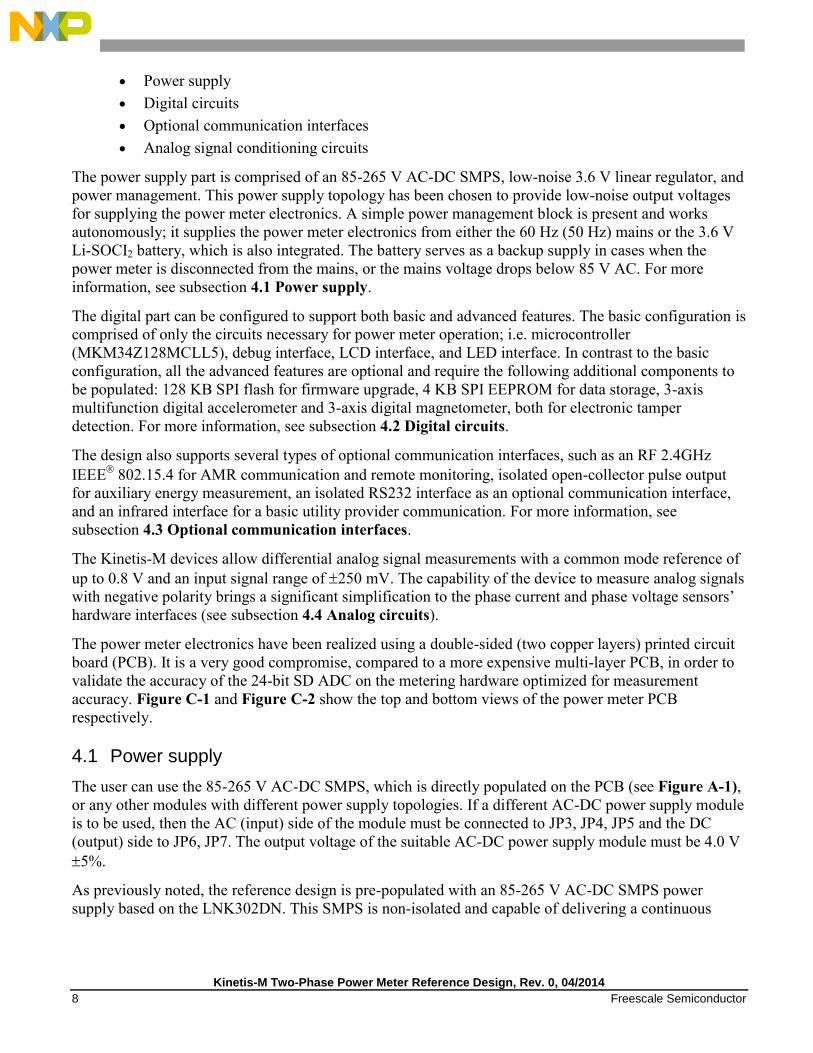
4.2.5 128 KB SPI flash
The 128 KB SPI flash (W25X10CLSN) can be used to store a new firmware application and/or load
profiles. The connection of the flash memory to the microcontroller is made through the SPI1 module, as
shown in Figure 4-4.
MMA_X
MMA_Y
MMA_Z
GND
U7PMMA8491Q
BYP1
NC
_1
11
1G
ND
6
VDD2
EN4
XOUT10
ZOUT8
NC
_1
21
2
YOUT9
SC
L5
SDA3
GND7
GND
I2C0_SCLR46 4.7K
MMA_EN
GND
C340.1UF
R45 4.7K
VAUX
C36
0.1UF
GND
VAUX
I2C0_SDA
U6MAG3110
CAP_A1
VD
D2
NC3
CAP_R4
GN
D1
5
SDA6SCL7V
DD
IO8
INT19
GN
D2
10
I2C0_SCLI2C0_SDA
C300.1UF
C330.1UF
C350.1UFGND
GND
GND
C310.1UF
VAUX
GND
C29 1uF
INT1
TP11
Kinetis-M Two-Phase Power Meter Reference Design, Rev. 0, 04/2014
12 Freescale Semiconductor
The SPI1 module of the MKM34Z128MCLL5 device supports a communication speed of up to 12.5
Mbit/s. This memory is supplied from the regulated output voltage (VPWR), hence it operates when the
power meter is supplied from the mains (normal operation mode).
Figure 4-4. 128 KB SPI flash control
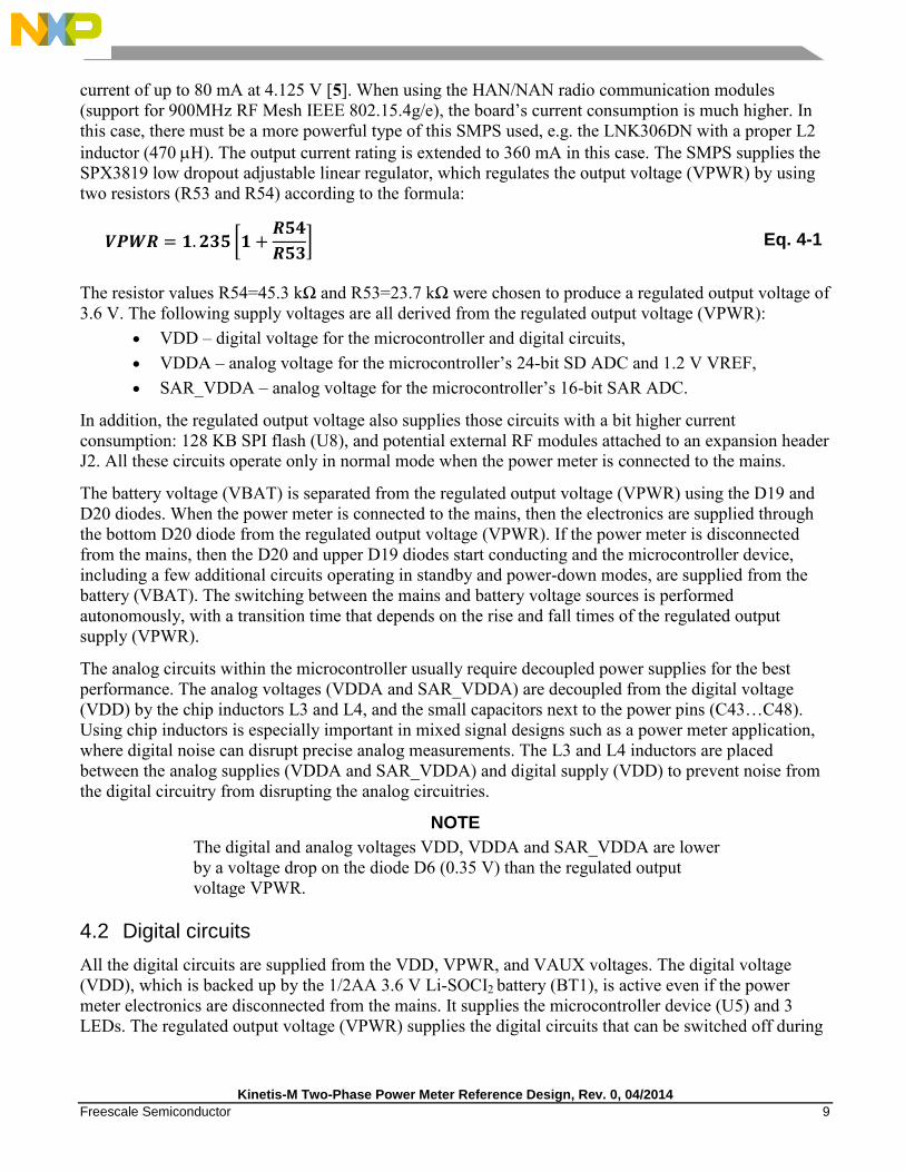
4.2.6 4 KB SPI EEPROM
The 4 KB SPI EEPROM (CAT25040VE) can be used for parameter storage (backup of the calibration
parameters). The connection of the EEPROM memory to the microcontroller is made through the SPI0
module, as shown in Figure 4-5. Because of the very small supply current of this memory, it is powered
directly by the PTF2 pin of the microcontroller (VAUX). Powering from the pin allows the
microcontroller to switch off the memory, and thus minimize current consumption in the standby mode.
The maximum communication throughput is limited by the CAT25040VE device to 10 Mbit/s. The
memory is prepared to work in normal and standby operation modes.
Figure 4-5. 4 KB SPI EEPROM control
4.3 Optional communication interfaces
Apart from the main unidirectional communication interface (see subsection 4.2.2-Output LEDs), the
meter also supports several types of optional communication interfaces that extend its usage. The main
components of these interfaces are: isolated RS232 interface (U2, U3), isolated open-collector pulse
output interface (U1), an expansion header (J2) for some RF daughter card, and an infrared interface. All
of these communication interfaces are intended to run in the normal operation mode only.
4.3.1 RF interfaces
The expansion header J2 (see Figure 4-6) is intended to interface the power meter with two types of
Freescale‟s ZigBee small factor radio modules. Firstly, it supports an RF MC1323x-IPB radio module
based on 2.4GHz IEEE 802.15.4. Secondly, it supports the K11 expansion board (for a schematic, see
GND
W25X10CLSNU8
DNP
CS1
DO/IO12
WP3
GND
4
DI/IO05
CLK6
HOLD7
VCC
8
R47 10K
DNP
C370.1UFDNP
GND
VPWR
VPWR
SPI1_SCK
SPI1_MOSI SPI1_MISO
FL
AS
H_
SS
GND
CAT25040VEU4
CS1
SO2
WP3
VSS
4
SI5
SCK6
HOLD7
VCC
8
R37 10K
C210.1UF
SPI0_MOSI
SPI0_SCK
SPI0_MISO
VAUX
GND SP
I0_
SS

Kinetis-M Two-Phase Power Meter Reference Design, Rev. 0, 04/2014
Freescale Semiconductor 13
Appendix B), which is used for connecting two HAN/NAN small radio sub-modules based on 900MHz
RF Mesh IEEE 802.15.4g/e and 6loWPAN/IPv6 connectivity (not included in the schematic in
Appendix B). The J2 expansion header provides the regulated output voltage VPWR to supply these RF
communication modules. Therefore, all modules should accept a supply voltage of 3.6 V with a
continuous current of up to 60 mA (MC1323x-IPB) or up to 150 mA (K11 HAN/NAN board with two
RF sub-modules). Both RF daughter cards need different MCU peripherals, therefore the J2 expansion
header supports connections to SPI1, SCI3 and the I2C1 peripherals, as well as to several I/O lines for
modules reset, handshaking, and control.
Figure 4-6. RF interfaces control
NOTE
Only one RF daughter card can be operated at one time inside the meter,
that is, the MC1323x-IPB or the K11 HAN/NAN with two RF sub-
modules.
4.3.2 Isolated open-collector pulse output interface
Figure 4-7 shows the schematic diagram of the open collector pulse output. This may be used for
switching loads with a continuous current as high as 50 mA and with a collector-to-emitter voltage of up
to 70 V. The interface is controlled through the peripheral crossbar (PXBAR_OUT7) pin of the
microcontroller, and hence it may be controlled by a variety of internal signals, for example timer
channels generating pulse outputs. The isolated open-collector pulse output interface is accessible on
connector J3.
Figure 4-7. Open-collector pulse output control
NOTE
The J3 output connector is not bonded to the meter‟s enclosure. Therefore,
the described interface is primarily used at the time of development
(uncovered equipment).
4.3.3 IR interface
The power meter has a galvanic isolated optical communication port, as per IEC 1107 (Japan version) or
ANSI C12.18 (U.S. version), so that it can be easily connected to a hand-held common meter reading
J2
CON_2X10
1 23 4
657 89 10
11 1213 1415 1617 1819 20
SCI3_TX[3]SCI3_RX[3]
RF_CTRL[3]RF_IO[3]
SCI3_RTS[3]SCI3_CTS[3]
RF_RST[3]SPI1_SCK[3]
SPI1_MOSI[3]
I2C1_SCL[3]
I2C1_SDA[3]
C9 0.1UF
R274.7K
R264.7K
GND
VPWRGND
SPI1_SS[3]
SPI1_MISO[3]
EOC[3]
J3
HDR 1X2
12
U1
SFH6106-4
1
2 3
4
R29
390.0
VDD
Kinetis-M Two-Phase Power Meter Reference Design, Rev. 0, 04/2014
14 Freescale Semiconductor
instrument for data exchange. The IR interface is driven by the SCI0. The IR interface schematic part is
shown in the Figure 4-8. Because of the very small supply current of the NPN phototransistor (Q1), it is
powered directly by the PTF2 (PTF7) pin of the microcontroller. Powering from the pin allows the
microcontroller to switch off the phototransistor circuit, and thus minimize current consumption in the
standby mode.
Figure 4-8. IR control
NOTE
Alternatively, this interface can be also used for waking up the meter
(from power-down to standby mode) by an external optical probe. This
feature has impact of increasing the current consumption in both operation
modes.
4.3.4 Isolated RS232 interface
This communication interface is used primarily for real-time visualization using FreeMASTER [6]. The
communication is driven by the SCI1 module of the microcontroller. Communication is optically isolated
through the optocouplers U2 and U3. Besides the RXD and TXD communication signals, the interface
implements two additional control signals, RTS and DTR. These signals are usually used for
transmission control, but this function is not used in the application. As there is a fixed voltage level on
these control lines generated by the PC, it is used to supply the secondary side of the U2 and the primary
side of the U3 optocouplers. The communication interface, including the D9…D11, C10, R30, and R32
components, required to supply the optocouplers from the transition control signals, is shown in Figure
4-9.
Figure 4-9. RS232 control
C112200PF
R33
10K
SCI0_TX[3]
SCI0_RX[3]
GND
GND
GND
~2.65mA @ 3.3V
R35 680
TP10
TP9
D12
TSAL4400
A C
Q1OP506B
21
R34
1.0K
VAUX2
SCI1_TX[3]
SCI1_RX[3]
D10MMSD4148T1G
DNP
AC
R32 470
DNP
D11
MMSD4148T1GDNP
AC
J4
HDR_2X5
DNP
1 23 4
657 89 10
VDD
U2
SFH6106-4DNP
1
2 3
4
U3
SFH6106-4DNP
1
23
4
R28
390.0DNP
R311.0KDNP
GND
R30 4.7K
DNP
D9
MMSD4148T1GDNP
A C
C102.2uFDNP
Max. 19200 Bd

Kinetis-M Two-Phase Power Meter Reference Design, Rev. 0, 04/2014
Freescale Semiconductor 15
NOTE
The J4 output connector is not bonded to the meter‟s enclosure. Therefore,
the described interface is primarily used at the time of development
(uncovered equipment).
4.4 Analog circuits
An excellent performance of the metering AFE, including external analog signal conditioning, is crucial
for a power meter application. The most critical is the phase current measurement, due to the high
dynamic range of the current measurement (typically 2000:1) and the relatively low input signal range
(from microvolts to several tens of millivolts). All analog circuits are described in the following
subsections.
4.4.1 Phase current measurement
The Kinetis-M two-phase power meter reference design is optimized primarily for current transformers
measurement. Alternatively, the Rogowski coils can be also used. Unfortunately, the shunt resistors
cannot be used here due to a strict requirement for the galvanic isolation between each phase. The
interface of a current sensor to the MKM34Z128MCLL5 device is very simple. Because of the two-
phase meter, this part of the interface is doubled (see Figure 4-10). Firstly, there are burden resistors
(R15+R18 and R21+R24) which transform currents from both the CT sensors to voltages. The values of
these burden resistors are adjusted to have a 0.25 V peak on each individual AFE input. This is due to
using the whole AFE range for the maximum phase current (see the tables in Section 1.1 for the meter‟s
specification). Secondly, there are anti-aliasing low-pass first order RC filters attenuating signals with
frequencies greater than the Nyquist frequency. The cut-off frequency of each individual analog filter
implemented on the board is 33.863 kHz; such a filter has an attenuation of 39.15 dB at the Nyquist
frequency of 3.072 MHz.
Figure 4-10. Phase currents signal conditioning circuit
R151.5
R211.5
R181.5
R241.5
C6
0.1UF
TP6
Sensor Mains ScalingR15,R18
R21,R24
1.5 CT 1:2000 U.S. 235 Amps
5.6 CT 1:2000 Japan 63 Amps
TP8
C8
0.1UF
J1
HDR 1X4
1234
R19
47.0
R14
47.0
CT1=1:2000
GNDA
CT1_OUT
C50.1UF
GNDA
CT1_IN
CT2_IN
CT2_OUT
GNDA
PHASE 1
R25
47.0
R20
47.0
GNDA
C70.1UF
CT2=1:2000
PHASE 2
SDADP1[3]
SDADM1[3]
SDADM0[3]
SDADP0[3]
TP5
TP7
Kinetis-M Two-Phase Power Meter Reference Design, Rev. 0, 04/2014
16 Freescale Semiconductor
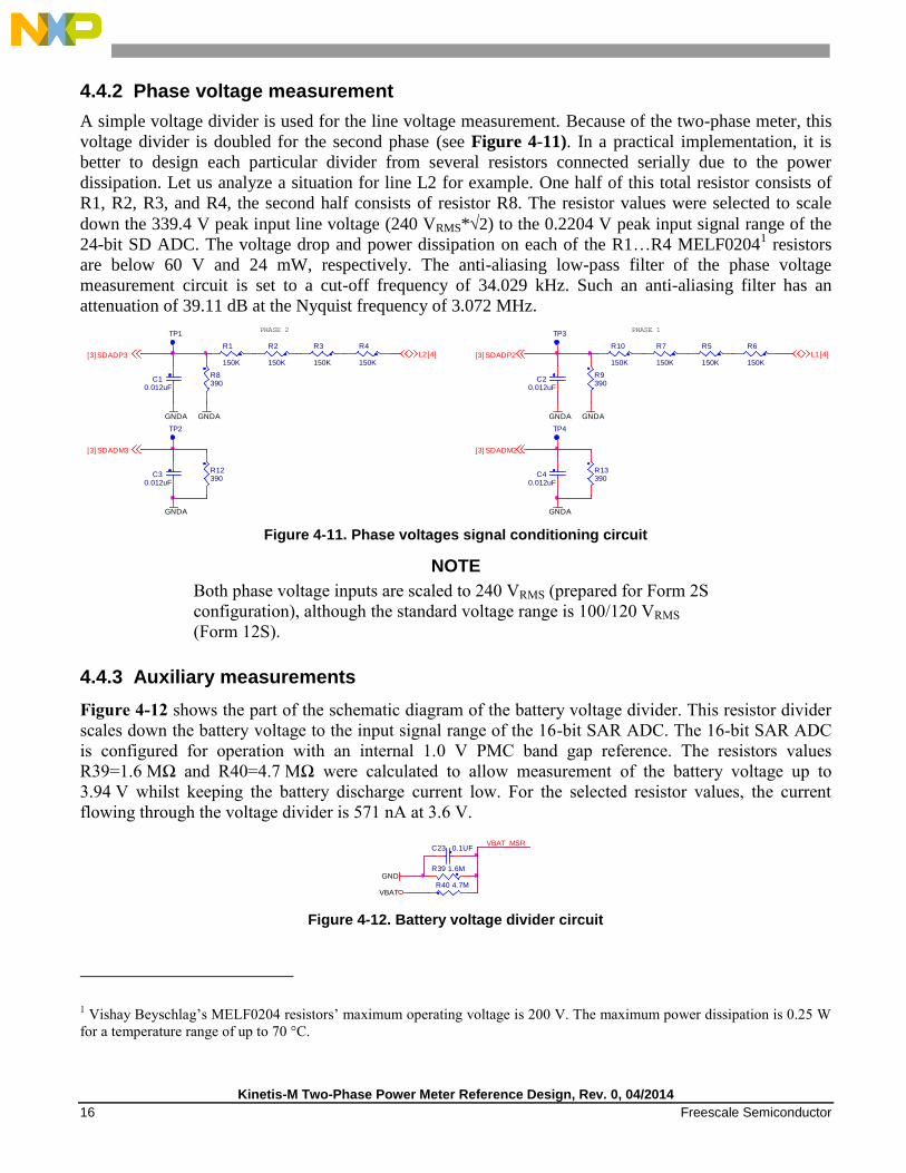
4.4.2 Phase voltage measurement
A simple voltage divider is used for the line voltage measurement. Because of the two-phase meter, this
voltage divider is doubled for the second phase (see Figure 4-11). In a practical implementation, it is
better to design each particular divider from several resistors connected serially due to the power
dissipation. Let us analyze a situation for line L2 for example. One half of this total resistor consists of
R1, R2, R3, and R4, the second half consists of resistor R8. The resistor values were selected to scale
down the 339.4 V peak input line voltage (240 VRMS*2) to the 0.2204 V peak input signal range of the
24-bit SD ADC. The voltage drop and power dissipation on each of the R1…R4 MELF02041 resistors
are below 60 V and 24 mW, respectively. The anti-aliasing low-pass filter of the phase voltage
measurement circuit is set to a cut-off frequency of 34.029 kHz. Such an anti-aliasing filter has an
attenuation of 39.11 dB at the Nyquist frequency of 3.072 MHz.
Figure 4-11. Phase voltages signal conditioning circuit
NOTE
Both phase voltage inputs are scaled to 240 VRMS (prepared for Form 2S
configuration), although the standard voltage range is 100/120 VRMS
(Form 12S).
4.4.3 Auxiliary measurements
Figure 4-12 shows the part of the schematic diagram of the battery voltage divider. This resistor divider
scales down the battery voltage to the input signal range of the 16-bit SAR ADC. The 16-bit SAR ADC
is configured for operation with an internal 1.0 V PMC band gap reference. The resistors values
R39=1.6 MΩ and R40=4.7 MΩ were calculated to allow measurement of the battery voltage up to
3.94 V whilst keeping the battery discharge current low. For the selected resistor values, the current
flowing through the voltage divider is 571 nA at 3.6 V.
Figure 4-12. Battery voltage divider circuit
1 Vishay Beyschlag‟s MELF0204 resistors‟ maximum operating voltage is 200 V. The maximum power dissipation is 0.25 W
for a temperature range of up to 70 °C.
R9390
R13390
R8390
R12390
C20.012uF
C40.012uF
GNDA GNDA
GNDA
C10.012uF
C30.012uF
GNDA
GNDA
GNDA
L1[4]L2[4]
PHASE 1PHASE 2
R1
150K
R2
150K
R3
150K
SDADM2[3]
R4
150KSDADP2[3]SDADP3[3]
SDADM3[3]
R10
150K
R7
150K
R5
150K
R6
150K
TP1
TP2
TP3
TP4
C23 0.1UF
R40 4.7M
GND
VBAT
R39 1.6M
VBAT_MSR

Kinetis-M Two-Phase Power Meter Reference Design, Rev. 0, 04/2014
Freescale Semiconductor 17
Status information on whether the power meter is connected or disconnected from the mains is critical
for transitioning between the power meter operating modes. The presence of a mains AC voltage is
signaled by the logic signal PWR_MSR (see the following figure) that is derived from the regulated
output voltage (VPWR). If the power meter is connected to the mains (VPWR=3.6 V), the PWR_MSR
will transition to 3.15 V and the software will read this signal from the PTC5 pin as logic 1. On the other
hand, a power meter disconnected from the mains will be read by the microcontroller device as logic 0.
Figure 4-13. Supply voltage divider circuit
5 Software design
This section describes the software application of the Kinetis-M two-phase power meter reference
design. The software application consists of measurement, calculation, calibration, user interface, and
communication tasks.
5.1 Block diagram
The application software has been written in C-language and compiled using the IAR Embedded
Workbench for ARM (version 6.40.2) with high optimization for execution speed (except for loop
unrolling). The software application is based on the Kinetis-M bare-metal software drivers [7] and the
FFT-based metering algorithm library [2] [3].
The software transitions between operating modes, performs a power meter calibration after first start-up,
calculates all metering quantities, controls the active and reactive energies pulse outputs, controls the
LCD, stores and retrieves parameters from the NVMs, and allows application remote monitoring and
control. The application monitoring and control is performed through FreeMASTER.
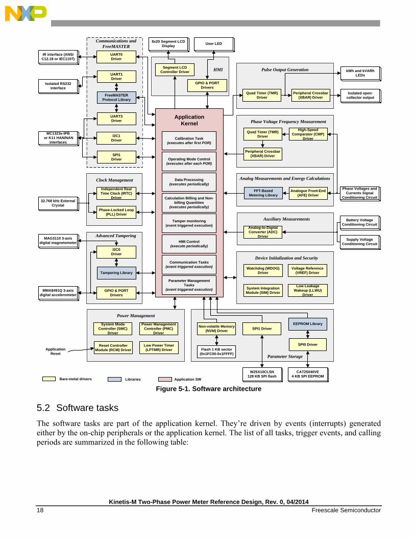
The following figure shows the software architecture of the power meter including interactions of the
software peripheral drivers and application libraries with the application kernel. All tasks executed by the
Kinetis-M two-phase power meter software are briefly explained in the following subsections.
VPWR
C22 0.1UF PWR_MSR
R38 330K
R36 47K
GND
Kinetis-M Two-Phase Power Meter Reference Design, Rev. 0, 04/2014
18 Freescale Semiconductor
Figure 5-1. Software architecture
5.2 Software tasks
The software tasks are part of the application kernel. They‟re driven by events (interrupts) generated
either by the on-chip peripherals or the application kernel. The list of all tasks, trigger events, and calling
periods are summarized in the following table:
Power Management
Phase-Locked Loop
(PLL) Driver
Reset Controller
Module (RCM) Driver
Power Management
Controller (PMC)
Driver
Application
Kernel
Non-volatile Memory
(NVM) Driver
Analogue Front-End
(AFE) Driver
Parameter Storage
Flash 1 KB sector
(0x1FC00-0x1FFFF)
SPI1 Driver
W25X10CLSN
128 KB SPI flash
SPI0 Driver
CAT25040VE
4 KB SPI EEPROM
Analog Measurements and Energy Calculations
High-Speed
Comparator (CMP)
Driver
Phase Voltages and
Currents Signal
Conditioning Circuit
Quad Timer (TMR)
Driver
Pulse Output Generation
Phase Voltage Frequency Measurement
Peripheral Crossbar
(XBAR) Driver
kWh and kVARh
LEDs
Quad Timer (TMR)
Driver
Peripheral Crossbar
(XBAR) DriverIsolated open-
collector output
Communications and
FreeMASTER
MC1323x-IPB
or K11 HAN/NAN
interfaces
Application
Reset
System Mode
Controller (SMC)
Driver
Clock Management
IR interface (ANSI
C12.18 or IEC1107)
UART0
Driver
Isolated RS232
interface
UART1
Driver
UART3
Driver
I2C1
Driver
SPI1
Driver
Analog-to-Digital
Converter (ADC)
Driver
Auxiliary Measurements Battery Voltage
Conditioning Circuit
Supply Voltage
Conditioning Circuit
FFT-Based
Metering Library
Independent Real
Time Clock (IRTC)
Driver32.768 kHz External
Crystal
MMA8491Q 3-axis
digital accelerometer
Advanced Tampering
8x20 Segment LCD
Display
HMISegment LCD
Controller Driver
GPIO & PORT
Drivers
User LED
GPIO & PORT
Drivers
I2C0
Driver
Watchdog (WDOG)
Driver
System Integration
Module (SIM) Driver
Device Initialization and Security
Low Leakage
Wakeup (LLWU)
Driver
Data Processing
(executes periodically)
Low Power Timer
(LPTMR) Driver
Voltage Reference
(VREF) Driver
Calibration Task
(executes after first POR)
HMI Control
(execute periodically)
Operating Mode Control
(executes after each POR)
Communication Tasks
(event triggered execution)
Parameter Management
Tasks
(event triggered execution)
Calculation Billing and Non-
billing Quantities
(executes periodically)
Tamper monitoring
(event triggered execution)
FreeMASTER
Protocol Library
MAG3110 3-axis
digital magnetometer
Bare-metal drivers Libraries Application SW
Tampering Library
EEPROM Library
Kinetis-M Two-Phase Power Meter Reference Design, Rev. 0, 04/2014
Freescale Semiconductor 19
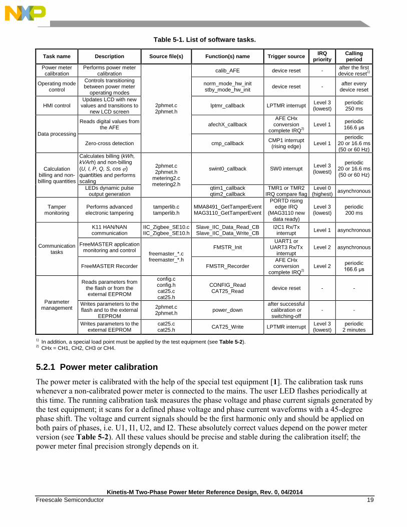
Table 5-1. List of software tasks.
1) In addition, a special load point must be applied by the test equipment (see Table 5-2).
2) CHx = CH1, CH2, CH3 or CH4.
5.2.1 Power meter calibration
The power meter is calibrated with the help of the special test equipment [1]. The calibration task runs
whenever a non-calibrated power meter is connected to the mains. The user LED flashes periodically at
this time. The running calibration task measures the phase voltage and phase current signals generated by
the test equipment; it scans for a defined phase voltage and phase current waveforms with a 45-degree
phase shift. The voltage and current signals should be the first harmonic only and should be applied on
both pairs of phases, i.e. U1, I1, U2, and I2. These absolutely correct values depend on the power meter
version (see Table 5-2). All these values should be precise and stable during the calibration itself; the
power meter final precision strongly depends on it.
Task name Description Source file(s) Function(s) name Trigger source IRQ
priority Calling period
Power meter calibration
Performs power meter calibration
2phmet.c 2phmet.h
calib_AFE device reset - after the first device reset
1)
Operating mode control
Controls transitioning between power meter
operating modes
norm_mode_hw_init stby_mode_hw_init
device reset - after every
device reset
HMI control Updates LCD with new
values and transitions to new LCD screen
lptmr_callback LPTMR interrupt Level 3 (lowest)
periodic 250 ms
Data processing
Reads digital values from the AFE
afechX_callback AFE CHx
conversion complete IRQ
2) Level 1
periodic 166.6 μs
Zero-cross detection cmp_callback CMP1 interrupt
(rising edge) Level 1
periodic 20 or 16.6 ms (50 or 60 Hz)
Calculation billing and non-billing quantities
Calculates billing (kWh, kVArh) and non-billing
(U, I, P, Q, S, cos ) quantities and performs scaling
2phmet.c 2phmet.h
metering2.c metering2.h
swint0_callback SW0 interrupt Level 3 (lowest)
periodic 20 or 16.6 ms (50 or 60 Hz)
LEDs dynamic pulse output generation
qtim1_callback qtim2_callback
TMR1 or TMR2 IRQ compare flag
Level 0 (highest)
asynchronous
Tamper monitoring
Performs advanced electronic tampering
tamperlib.c tamperlib.h
MMA8491_GetTamperEvent MAG3110_GetTamperEvent
PORTD rising edge IRQ
(MAG3110 new data ready)
Level 3 (lowest)
periodic 200 ms
Communication tasks
K11 HAN/NAN communication
IIC_Zigbee_SE10.c IIC_Zigbee_SE10.h
Slave_IIC_Data_Read_CB Slave_IIC_Data_Write_CB
I2C1 Rx/Tx interrupt
Level 1 asynchronous
FreeMASTER application monitoring and control
freemaster_*.c freemaster_*.h
FMSTR_Init UART1 or
UART3 Rx/Tx interrupt
Level 2 asynchronous
FreeMASTER Recorder FMSTR_Recorder AFE CHx
conversion complete IRQ
2) Level 2
periodic 166.6 μs
Parameter management
Reads parameters from the flash or from the external EEPROM
config.c config.h cat25.c cat25.h
CONFIG_Read CAT25_Read
device reset - -
Writes parameters to the flash and to the external
EEPROM
2phmet.c 2phmet.h
power_down after successful
calibration or switching-off
- -
Writes parameters to the external EEPROM
cat25.c cat25.h
CAT25_Write LPTMR interrupt Level 3 (lowest)
periodic 2 minutes
Kinetis-M Two-Phase Power Meter Reference Design, Rev. 0, 04/2014
20 Freescale Semiconductor
Table 5-2. List of calibration load points
Power meter version Current range INOM(IMAX) [A]
Voltage load point UNOM [V]
Current load point INOM [A]
Frequency [Hz]
U to I phase shift [degree]
U.S.: ANSI C12.20 (Form 12S) 30(200) 120 30 60 (50) 45
Japan: IEC62053-22 5(60) 100 5 50 (60) 45
Each voltage and current load point is applied with two different frequencies (50 and 60 Hz)
independently. It is not mandatory, but thanks to this, the calibrated power meter is prepared for working
with different mains around the world. If the calibration task detects such a load point, then the
calibration task calculates the calibration gains, and phase shift using the following formulas:
Eq. 5-1
Eq. 5-2
Eq. 5-3
Where:
, are unsigned 16-bit values of both the voltage and power gains for a known frequency;
these are used in the scaling_power function after calibration,
is the signed 16-bit value of the calculated phase shift caused by parasitic inductance of the
current transformer for a known frequency; it is used in the AFE channel delay register after
calibration (in the afe_chan_init function),
j-index is the number of the phase (0=Phase 1, 1=Phase 2),
, are calibration (load) points (see Table 5-2),
, are scaled non-billing quantities measured by the non-calibrated meter,
, are scaled computed quantities: ; ,
is the divide factor (4 for the U.S. meter and 1 for the Japan meter).
NOTE
The AFE offsets are not calibrated due to the metering algorithm used,
which ignores this phenomenon for power computing [2].
The calibration task terminates by storing the calibration gains and phase shifts into two non-volatile
memories; the internal flash memory and the external EEPROM memory (backup storage). The whole
calibration process is terminated by resetting the microcontroller device finally. The recalibration of the
power meter can be re-initiated later from the FreeMASTER tool by rewriting the Calibration status
flag.
NOTE
The user LED is permanently turned off after successful calibration.
5.2.2 Operating mode control
The transitioning of the power meter electronics between operating modes helps maintain a long battery
lifetime. The power meter software application supports the following operating modes:
Normal (electricity is supplied, causing the power meter to be fully-functional)
Kinetis-M Two-Phase Power Meter Reference Design, Rev. 0, 04/2014
Freescale Semiconductor 21
Standby (electricity is disconnected, and the user can see the latest kWh value on the LCD
for a limited time, 2.5 seconds)
Power-down (electricity is disconnected with no user interaction)
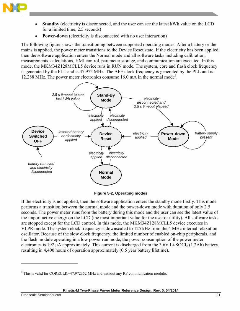
The following figure shows the transitioning between supported operating modes. After a battery or the
mains is applied, the power meter transitions to the Device Reset state. If the electricity has been applied,
then the software application enters the Normal mode and all software tasks including calibration,
measurements, calculations, HMI control, parameter storage, and communication are executed. In this
mode, the MKM34Z128MCLL5 device runs in RUN mode. The system, core and flash clock frequency
is generated by the FLL and is 47.972 MHz. The AFE clock frequency is generated by the PLL and is
12.288 MHz. The power meter electronics consume 16.0 mA in the normal mode2.
Figure 5-2. Operating modes
If the electricity is not applied, then the software application enters the standby mode firstly. This mode
performs a transition between the normal mode and the power-down mode with duration of only 2.5
seconds. The power meter runs from the battery during this mode and the user can see the latest value of
the import active energy on the LCD (the most important value for the user or utility). All software tasks
are stopped except for the LCD control. In this mode, the MKM34Z128MCLL5 device executes in
VLPR mode. The system clock frequency is downscaled to 125 kHz from the 4 MHz internal relaxation
oscillator. Because of the slow clock frequency, the limited number of enabled on-chip peripherals, and
the flash module operating in a low power run mode, the power consumption of the power meter
electronics is 192 μA approximately. This current is discharged from the 3.6V Li-SOCI2 (1.2Ah) battery,
resulting in 4,400 hours of operation approximately (0.5 year battery lifetime).
2 This is valid for CORECLK=47.972352 MHz and without any RF communication module.
Power-down
Mode
Stand-By
Mode
Normal
Mode
Device
Reset
Device
Switched
OFF
inserted battery or electricity
applied
electricity applied
electricity disconnected
electricity disconnected and
2.5 s timeout elapsed
electricity applied
2.5 s timeout to see last kWh value
battery removed and electricity disconnected
electricitydisconnected
electricity applied
battery supply present
Kinetis-M Two-Phase Power Meter Reference Design, Rev. 0, 04/2014
22 Freescale Semiconductor
Finally, when the duration of the standby mode has elapsed, the power meter goes into the power-down
mode. The MKM34Z128MCLL5 device is forced to enter VLLS0 mode, where recovery is only possible
when the mains is supplied. The power meter runs from the 3.6V Li-SOCI2 (1.2Ah) battery during this
mode. The power-down mode is characterized by a battery current consumption of 2.6 μA, which results
in 270,000 hours of operation approximately (more than 20 year battery lifetime).
5.2.3 Data processing
Reading the phase voltage and phase current samples from the analog front-end (AFE) occurs
periodically every 166.6 μs. This task runs on the high priority level and is triggered asynchronously
when the AFE result registers receive new samples. The task reads the phase voltage and phase current
samples from four AFE result registers (two voltages and two currents), and writes these values to the
buffers for use by the calculation task.
Another separate task monitors the mains zero-crossings, which is necessary for starting the main
calculation process by a software interrupt (one complete calculation process per one signal period). This
task also backs up the buffers with current AFE results to prevent an overwrite of these values by new
AFE results.
5.2.4 Calculations
The execution of the calculation task is carried out when the SW0 interrupt is generated. This interrupt is
caused by a zero-crossing of the input signal. This is done periodically at the beginning of each signal
period. At this time, all circle buffers are filled up with the AFE results from the previous signal period.
Therefore, the execution period of the calculation task depends on the input signal frequency. The
calculation task performs the power computation by the PowerCalculation function, according to the
metering algorithm used ([2] [3]), and also scales the results by the scaling_power function, using the
calibration gains obtained during the calibration phase:
Eq. 5-4
Eq. 5-5
Eq. 5-6
Eq. 5-7
Where: , , are scaled non-billing values,
, are calibration parameters (see Section 5.2.1),
, , , are FFT outputs; not scaled, and non-billing values,
, are voltage and power divide constants for rough basic scaling,
j-index is the number of the phase (0=Phase 1, 1=Phase 2).
These scaled non-billing values are used for computing the billing values (energies) by the
EnergyCalculation function consecutively, and also for producing a low-jitter, high dynamic range pulse
output waveform for two energy LEDs (kWh and KVArh).
Kinetis-M Two-Phase Power Meter Reference Design, Rev. 0, 04/2014
Freescale Semiconductor 23
NOTE
and values are computed indirectly in the HMI task (see
Section 5.2.5).
5.2.5 HMI control
The Human Machine Interface (HMI) control task executes in a 250 ms loop and on the lowest priority
(Level 3). It reads the real-time clock, calculates the mains frequency, runs the calibration task (see
Section 5.2.1), computes any remaining non-billing quantities ( , ), and formats data into a
string that is displayed on the LCD. Because there is no user push-button in the meter, this task also deals
with scrolling the values on the LCD every 5 seconds (see Table 6-1). This task also provides both the
phase and gains compensation according to the measured frequency ( , , and
parameters).
5.2.6 Tamper monitoring
Because there isn‟t any mechanical push-button used for tamper detection, the meter uses an advanced
electronic version. This includes two types of 3-axis sensor, one for cover opening detection
(MMA8491Q) and the other for magnetic tamper detection (MAG3110). The application software
supports a full tamper library for controlling these sensors. The communication with these sensors is
based on an interrupt, which comes periodically from the MAG3110 sensor when new data is ready. The
relevant interrupt service routine is not only used for reading the MAG3110 output, but also for scanning
the MMA8491Q sensor, which doesn‟t generate any interrupt.
5.2.7 Communication tasks
5.2.7.1 FreeMASTER communication task
The FreeMASTER establishes a data exchange with the PC. The communication is fully driven by the
UART1 or UART3 Rx/Tx interrupts, which generate interrupt service calls with priority Level 2. The
priority setting guarantees that data processing and calculation tasks are not impacted by the
communication. Assigning the right UART port is selected by the SCIx_PORT program constant in the
freemaster_cfg.h file. For using the FreeMASTER on the RF 2.4 GHz interface (see Subsection 4.3.1-
RF interfaces), the SCIx_PORT constant should be set to 3, whereas for using on a basic isolated RS232
interface (see Subsection 4.3.4-Isolated RS232 interface), this constant should be set to 1. The power
meter acts as a slave device answering packets received from the master device (PC). The recorder
function is called inside the afechX_callback interrupt service routine every 166.6 μs. For more
information about using FreeMASTER, refer to Subsection 7- FreeMASTER visualization.
5.2.7.2 HAN/NAN communication task
This task is used for Home Area Network (HAN) and Neighborhood Area Network (NAN)
communication. The task is fully driven by the I2C1 Rx/Tx interrupt, which generates interrupt service
calls with priority Level 1. These are asynchronous interrupts. The HAN/NAN communication concept is
based on a wired communication between the metering MCU (MKM34Z128MCLL5), which is the
master, and the K11 HAN/NAN expansion board, which is the slave (from the I2C point of view). The
K11 expansion board contains the ZigBee IP Smart Energy 2.0 Profile stack for directly driving two

Kinetis-M Two-Phase Power Meter Reference Design, Rev. 0, 04/2014
24 Freescale Semiconductor
small RF radio modules, which are part of the K11 board. For more information, refer to Section 8-
HAN/NAN visualization.
5.2.8 Parameter management
The current software application uses the last 1024 bytes sector of the internal flash memory of the
MKM34Z128MCLL5 device for parameter storage. There is also an external 4 kB EPROM used for the
same purpose, but as a backup storage. The main purpose for using these NV memories is to save all the
calibration parameters. By default, parameters are written after a successful calibration and read after
each device reset. In addition, storing and reading parameters can be also initiated through the
FreeMASTER independently (see also Subsection 7- FreeMASTER visualization).
5.3 Performance
Table 5-3 shows the memory requirements of the Kinetis-M two-phase power meter software
application3.
Table 5-3. Memory requirements
Function Description Flash size
[KB] RAM size
[KB]
Application framework Complete application without all libraries and FreeMASTER 25.882 5.871
FFT-based metering library FFT-based metering algorithm library 6.484 -
Tamper library MAG3110 and MMA8491Q tamper library 1.524 0.02
EEPROM library CAT25040VE EEPROM library 0.738 -
FreeMASTER FreeMASTER protocol and serial communication driver 2.328 4.309
Grand Total 36.956 10.200
The software application reserves about 4 kB RAM for the FreeMASTER recorder. If the recorder is not
required, or a fewer number of variables will be recorded, you may reduce the size of this buffer by
modifying the FMSTR_REC_BUFF_SIZE constant (refer to the freemaster_cfg.h header file, line 81).
The system clock of the device is generated by the FLL (except for the AFE clock). In the normal
operating mode, the FLL multiplies the clock of an external 32.768 kHz crystal by a factor of 1464,
hence generating a low-jitter system clock with a frequency of 47.972352 MHz. Such a system clock
frequency is absolutely sufficient for executing the fully functional software application.
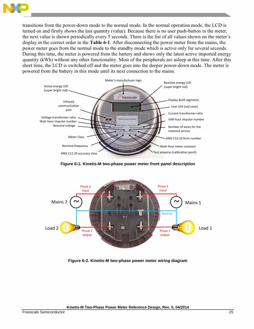
6 Application set-up
The following figures show both the front panel description and the 12S connection wiring diagram of
the Kinetis-M two-phase power meter.
Among the main capabilities of the power meter, is the registering of the active and reactive energy
consumed by an external load. After connecting the power meter to the mains, the power meter
3 Application is compiled using the IAR Embedded Workbench for ARM (version 6.40.2) with high optimization for
execution speed (except for Loop unrolling). Memory requirements are valid for S/W Rev. 2.0.0.2. (December 2013).
Kinetis-M Two-Phase Power Meter Reference Design, Rev. 0, 04/2014
Freescale Semiconductor 25
Mains 1
Phase 2 input
Neutral
~ ~
Phase 1 input
Mains 2
Load 1 Load 2
Phase 1 output
Phase 2 output
transitions from the power-down mode to the normal mode. In the normal operation mode, the LCD is
turned on and firstly shows the last quantity (value). Because there is no user push-button in the meter,
the next value is shown periodically every 5 seconds. There is the list of all values shown on the meter‟s
display in the correct order in the Table 6-1. After disconnecting the power meter from the mains, the
power meter goes from the normal mode to the standby mode which is active only for several seconds.
During this time, the meter is powered from the battery and shows only the latest active imported energy
quantity (kWh) without any other functionality. Most of the peripherals are asleep at this time. After this
short time, the LCD is switched off and the meter goes into the deeper power-down mode. The meter is
powered from the battery in this mode until its next connection to the mains.
Figure 6-1. Kinetis-M two-phase power meter front panel description
Figure 6-2. Kinetis-M two-phase power meter wiring diagram
Display 8x20 segments
Reactive energy LED (super bright red)
Infrared communication
port
Active energy LED (super bright red)
Current transformer ratio
Number of wires for the metered service
ANSI C12.10 form number
Watt-hour meter constant
Test amperes (calibration point) ANSI C12.20 accuracy class
Nominal frequency
Meter Class
Nominal voltage
Voltage transformer ratio VAR-hour impulse number
Watt-hour impulse number
Meter’s manufacturer logo
User LED (red color)
Kinetis-M Two-Phase Power Meter Reference Design, Rev. 0, 04/2014
26 Freescale Semiconductor
NOTE
This power meter can work in purely single-phase installations too. In this
case, use only the Phase 1 and Neutral inputs on the meter.
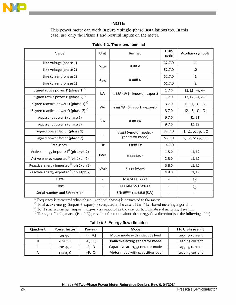
Table 6-1. The menu item list
Value Unit Format OBIS code
Auxiliary symbols
Line voltage (phase 1) VRMS #.## V
32.7.0 L1
Line voltage (phase 2) 52.7.0 L2
Line current (phase 1) ARMS #.### A
31.7.0 I1
Line current (phase 2) 51.7.0 I2
Signed active power P (phase 1) 4)
kW #.### kW (+ import, - export)
1.7.0 I1, L1,
Signed active power P (phase 2) 4)
1.7.0 I2, L2,
Signed reactive power Q (phase 1) 4)
VAr #.## VAr (+import, - export)
3.7.0 I1, L1, +Q, -Q
Signed reactive power Q (phase 2) 4)
3.7.0 I2, L2, +Q, -Q
Apparent power S (phase 1) VA #.## VA
9.7.0 I1, L1
Apparent power S (phase 2) 9.7.0 I2, L2
Signed power factor (phase 1)
- #.### (+motor mode, -
generator mode)
33.7.0 I1, L1, cos , I, C
Signed power factor (phase 2)
53.7.0 I2, L2, cos , I, C
Frequency1)
Hz #.### Hz 14.7.0 -
Active energy imported2)
(ph 1+ph 2) kWh #.### kWh
1.8.0 L1, L2
Active energy exported2)
(ph 1+ph 2) 2.8.0 L1, L2
Reactive energy imported3)
(ph 1+ph 2) kVArh #.### kVArh
3.8.0 L1, L2
Reactive energy exported3)
(ph 1+ph 2) 4.8.0 L1, L2
Date - MMM.DD.YYYY - Time - HH.MM.SS + WDAY -
Serial number and SW version - SN: #### + #.#.#.# (SW) - -
1) Frequency is measured when phase 1 (or both phases) is connected to the meter
2) Total active energy (import + export) is computed in the case of the Filter-based metering algorithm
3) Total reactive energy (import + export) is computed in the case of the Filter-based metering algorithm
4) The sign of both powers (P and Q) provide information about the energy flow direction (see the following table).
Table 6-2. Energy flow direction
Quadrant Power factor Powers Mode I to U phase shift
I cos , I +P, +Q Motor mode with inductive load Lagging current
II -cos , I -P, +Q Inductive acting generator mode Leading current
III -cos , C -P, -Q Capacitive acting generator mode Lagging current
IV cos , C +P, -Q Motor mode with capacitive load Leading current

Kinetis-M Two-Phase Power Meter Reference Design, Rev. 0, 04/2014
Freescale Semiconductor 27
There are two Freescale electronic tamper detection sensors inside the meter. Firstly, there is a
magnetometer sensor, which can detect a magnetic field caused by a strong external magnet. This sensor
works only in the normal operation mode. Secondly, there is an accelerometer sensor, which can detect
some unexpected movements of the meter itself or some parts of the meter, e.g. the front cover due to
tamper detection. When some tampering occurs, the applicable symbol appears on the LCD for a short
time. See also Figure 6-3 for description of the meter‟s entire display.
NOTE
The information about the tamper event is deliberately not saved into the
non-volatile memory due to repeated customer‟s evaluation.
Figure 6-3. Power meter display description
Both energy LEDs (kWh and kVArh) flash simultaneously with the internal energy counters during the
normal operation mode. LED kWh is the sum of both active energies (imported and exported) and LED
kVArh is the sum of both reactive energies (imported and exported). All these active and reactive energy
counters are periodically saved every 2 minutes into the external EEPROM memory (backup storage).
An applicable symbol for data saving flashes on the LCD at this time. These energy quantities remain in
the memory after resetting the Power Meter. To remotely clear these energy counters, you should use the
FreeMASTER application (see section 7-FreeMASTER visualization) and apply the REMOTE
COMMAND/CLEAR ENERGY COUNTERS command.
7 FreeMASTER visualization
The FreeMASTER data visualization software is used for data exchange [6]. The FreeMASTER software
running on a PC communicates with the Kinetis-M two-phase power meter over a defined interface. This
communication is interrupt driven and is active when the power meter is powered from the mains. The
FreeMASTER software allows remote visualization, parameterization and calibration of the power
meter. It runs visualization scripts which are embedded into a FreeMASTER project file.
There can be several types of defined interfaces used for communication between the meter itself and the
remote PC:
2.4GHz RF interface based on the IEEE 802.15.4 standard (default interface),
An isolated RS232 interface (not bonded to the meter‟s enclosure, for development only),
An infrared interface (optional only).
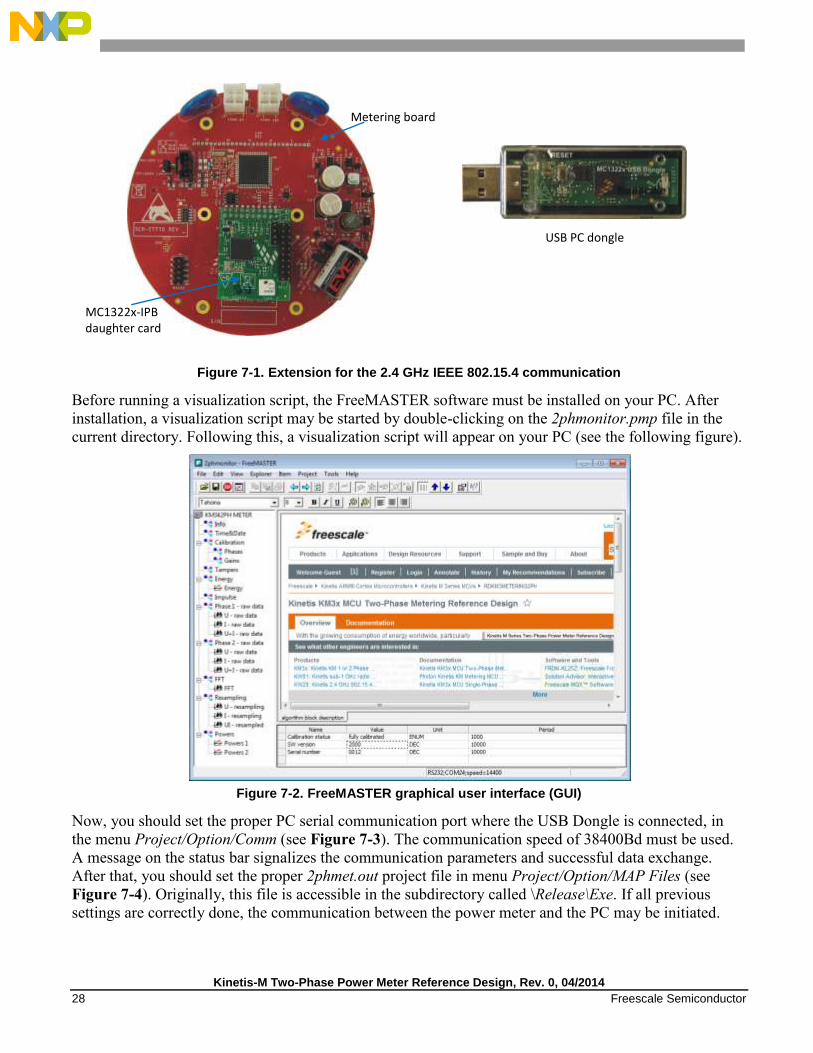
For the hardware formation of the communication based on the 2.4GHz RF interface, an internal
MC1322x-IPB daughter card should be connected inside the meter to the J2 connector (see Figure 7-1)
and the USB Dongle to the PC. The FreeMASTER software running on the PC side shall be used for the
data exchange.
Auxiliary symbols Magnetometer tamper event symbol
Accelerometer tamper event symbol
Main value
Unit of the main value OBIS code
Symbol for saving to NV memory
Kinetis-M Two-Phase Power Meter Reference Design, Rev. 0, 04/2014
28 Freescale Semiconductor
Figure 6-3-1-1-1-1-1-1-1.
Figure 6-3-1-1-1-1-1-1-2.
Figure 6-3-1-1-1-1-1-1-3.
Figure 7-1. Extension for the 2.4 GHz IEEE 802.15.4 communication
Before running a visualization script, the FreeMASTER software must be installed on your PC. After
installation, a visualization script may be started by double-clicking on the 2phmonitor.pmp file in the
current directory. Following this, a visualization script will appear on your PC (see the following figure).
Figure 7-2. FreeMASTER graphical user interface (GUI)
Now, you should set the proper PC serial communication port where the USB Dongle is connected, in
the menu Project/Option/Comm (see Figure 7-3). The communication speed of 38400Bd must be used.
A message on the status bar signalizes the communication parameters and successful data exchange.
After that, you should set the proper 2phmet.out project file in menu Project/Option/MAP Files (see
Figure 7-4). Originally, this file is accessible in the subdirectory called \Release\Exe. If all previous
settings are correctly done, the communication between the power meter and the PC may be initiated.
Metering board
MC1322x-IPB daughter card
USB PC dongle
Kinetis-M Two-Phase Power Meter Reference Design, Rev. 0, 04/2014
Freescale Semiconductor 29
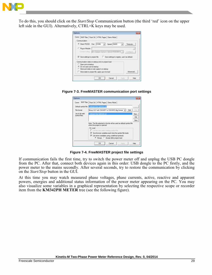
To do this, you should click on the Start/Stop Communication button (the third „red‟ icon on the upper
left side in the GUI). Alternatively, CTRL+K keys may be used.
Figure 7-3. FreeMASTER communication port settings
Figure 7-4. FreeMASTER project file settings
If communication fails the first time, try to switch the power meter off and unplug the USB PC dongle from the PC. After that, connect both devices again in this order: USB dongle to the PC firstly, and the power meter to the mains secondly. After several seconds, try to restore the communication by clicking on the Start/Stop button in the GUI.
At this time you may watch measured phase voltages, phase currents, active, reactive and apparent powers, energies and additional status information of the power meter appearing on the PC. You may also visualize some variables in a graphical representation by selecting the respective scope or recorder item from the KM342PH METER tree (see the following figure).
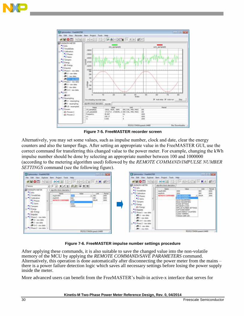
Kinetis-M Two-Phase Power Meter Reference Design, Rev. 0, 04/2014
30 Freescale Semiconductor
Figure 7-5. FreeMASTER recorder screen
Alternatively, you may set some values, such as impulse number, clock and date, clear the energy
counters and also the tamper flags. After setting an appropriate value in the FreeMASTER GUI, use the
correct command for transferring this changed value to the power meter. For example, changing the kWh
impulse number should be done by selecting an appropriate number between 100 and 1000000
(according to the metering algorithm used) followed by the REMOTE COMMAND/IMPULSE NUMBER
SETTINGS command (see the following figure).
Figure 7-6. FreeMASTER impulse number settings procedure
After applying these commands, it is also suitable to save the changed value into the non-volatile memory of the MCU by applying the REMOTE COMMAND/SAVE PARAMETERS command. Alternatively, this operation is done automatically after disconnecting the power meter from the mains – there is a power failure detection logic which saves all necessary settings before losing the power supply inside the meter.
More advanced users can benefit from the FreeMASTER’s built-in active-x interface that serves for

Kinetis-M Two-Phase Power Meter Reference Design, Rev. 0, 04/2014
Freescale Semiconductor 31
exchanging data with other signal processing and programming tools, such as Matlab, Excel, LabView, and LabWindows.
CAUTION
The user is not allowed to change any „red-marked decimal calibration
values‟ in the Calibration section.
8 HAN/NAN visualization
This Power Meter also supports an extension for Home Area Network (HAN) and Neighborhood Area
Network (NAN) communication. To do this, a K11 expansion daughter card with both Nivis and
Coconino radio sub-modules must be connected to the main metering board (see the following figure).
The K11 expansion board works as a mediator between the metering engine and both RF modules
(“sandwich concept”). Both radio modules, housed on the K11 daughter board, are RF-based, therefore
these require an antenna. The Coconino radio module has its own integrated antenna as part of the
printed circuit board, whereas the Nivis radio module needs an external, small and flexible antenna,
connected to the respective connector placed on its front side. This antenna perfectly fits into the meter‟s
enclosure. A software installation for the HAN/NAN communication procedure, connection with the
remote station, and description of its graphical user interface is not included in the content of this
document. It can be found in a separate document through the Freescale support [8].
Figure 8.1 Extension for the HAN/NAN connectivity
9 Accuracy and performance
As already indicated, the Kinetis-M two-phase reference designs have been fully calibrated using the test
equipment ELMA8303 [1], which comprises of a reference meter with a precision of 0.01 %. The U.S.
power meters were tested according to the ANSI C12.20-2002 American national standards for
Electricity Meters 0.2 and 0.5 accuracy classes, whereas the Japan power meters were tested according to
the IEC 62053-22 international standards for electronic meters of active energy classes 0.2S and 0.5S,
the IEC 62053-23 international standard for static meters of reactive energy classes 2 and 3, and the IEC
62052-11 international standards for electricity metering equipment.
Metering board
Coconino (HAN) radio module
Nivis (NAN) radio module
K11 HAN/NAN expansion daughter card
Antenna connector
Kinetis-M Two-Phase Power Meter Reference Design, Rev. 0, 04/2014
32 Freescale Semiconductor
During the calibration and testing process, the power meter measured electrical quantities generated by
the test bench ELMA8303, calculated the active and reactive energies, and generated pulses on the
output LEDs; each generated pulse was equal to the active and reactive energy amount kWh
(kVArh)/imp. The deviations between pulses generated by the power meter and reference pulses
generated by test equipment defined the measurement accuracy.
9.1 Room temperature accuracy testing
The following figure shows the calibration protocol of the typical Freescale two-phase ANSI (U.S.)
power meter. The protocol indicates the results of the power meter calibration performed at 25 °C. The
accuracy and repeatability of the measurement for various phase currents, and the angles between phase
current and phase voltage are shown in these graphs.
The first graph (on the top) indicates the accuracy of the active and reactive energy measurement after
calibration. The x-axis shows variation of the phase current, and the y-axis denotes the average accuracy
of the power meter computed from five successive measurements. Two bold red lines define the ANSI
C12.20-2002 Class 0.2 accuracy margins for active energy measurement for power factor 1.
The second graph (on the bottom) shows the measurement repeatability; i.e. standard deviation of error
of the measurements at a specific load point. Similarly to the power meter accuracy, the standard
deviation has also been computed from five successive measurements. The standard deviation is
approximately ten-times lesser than the meter‟s accuracy (compare the top and bottom graphs).
By analyzing the protocols of several Kinetis-M two-phase power meters, it can be said that this
equipment measures active and reactive energies at all power factors, a 25 °C ambient temperature, and
in the current range 0.9-200 A4, more or less with an accuracy range 0.1%.
4 The current range was scaled to IMAX = 235 A. It is valid for the ANSI (U.S.) version meter.
Kinetis-M Two-Phase Power Meter Reference Design, Rev. 0, 04/2014
Freescale Semiconductor 33
Figure 9.1 Calibration protocol at 25°C according to the ANSI C12.20-2002 class 0.2
9.2 Extended temperature accuracy testing
In addition to room temperature testing, the Kinetis-M two-phase power meter has been evaluated over
the extended operating temperature range (0 °C to 80 °C). This testing was carried out with the power
meter placed in a heat chamber. In order to speed up the measurement, only active energy accuracy has
been evaluated. The isolated open-collector pulse output interface has been used instead of the output
LED to provide active energy pulses to the test equipment for accuracy evaluation.
The following figure shows the accuracy of the power meter evaluated at an extended temperature range.
The temperature test was done on the Japan version of the two-phase power meter, therefore the accuracy
margins are defined by the IEC62053-22 Class 0.5 S. The extended accuracy margins are denoted by
respective bold lines for each temperature. The color of each margin is the same as the color of each
particular error curve. The calibration protocol shows that the active energy measured by the power
meter at all temperatures for a unity power factor fits within the accuracy margins mandated by the
standard with a temperature coefficient approximately 40 ppm/°C.
Kinetis-M Two-Phase Power Meter Reference Design, Rev. 0, 04/2014
34 Freescale Semiconductor
Figure 9.2 Calibration protocol for extended temperature range according to the IEC 62053-22 class 0.5S
10 Summary
This design reference manual describes a solution for a two-phase electronic power meter based on the
MKM34Z128CLL5 microcontroller.
Freescale semiconductor offers both FFT and Filter based metering algorithms for use in customer
applications. The former calculates metering quantities in the frequency domain, the latter in the time
domain. The reference manual explains the basic theory of power metering and lists all the equations to
be calculated by the power meter.
The hardware platform of the power meter is algorithm independent, so application firmware can
leverage any type of metering algorithm based on customer preference. In order to extend the power
meter uses, the hardware platform comprises a 128 KB SPI flash for firmware upgrade, 4 KB SPI
EEPROM for data storage, two Xtrinsic 3-axis digital sensors for enhanced tamper detection, and an
expansion header for two types of the RF daughter boards for AMR communication and monitoring.
The application software has been written in C-language and compiled using the IAR Embedded
Workbench for ARM (6.40 and higher), with optimization for the execution speed. It is based on the
Kinetis-M bare-metal software drivers [7] and the FFT-based metering library [2] [3] as default.
Alternatively, the Filter-based metering library can be also used [4]. The application firmware
automatically calibrates the power meter, calculates all metering quantities, controls active and reactive
energy pulse outputs, the LCD, stores and retrieves parameters from flash memory, and allows
monitoring the application, including recording selected waveforms through the FreeMASTER. The
application software of such complexity requires 36.9 KB of flash and 10.2 KB of RAM approximately.
The system clock frequency of the MKM34Z128CLL5 device must be 23.986176 MHz or higher to
calculate all metering quantities with an update rate of 6 kHz and with the 32 FFT points (16 harmonics
in total) consecutively.
Kinetis-M Two-Phase Power Meter Reference Design, Rev. 0, 04/2014
Freescale Semiconductor 35
This power meter can be produced in two H/W versions: the U.S. version according to the ANSI C12.20
standard, and the Japan version according to the IEC 62053-22 standard. The main H/W difference
between both versions is in the input current range, the S/W is the same.
The power meter is designed to transition between three operating modes. Firstly, in the normal
operating mode, the power meter is powered from the mains. The second mode, the so-called standby
mode, is a transition between the normal mode and the power-down mode with a duration of only several
seconds. The power meter runs from the battery during this mode and the user can see the latest value of
the import active energy on the LCD (the most important value). Finally, when the power meter
electronics automatically transitions from the standby mode to the power-down mode with the slowest
current consumption, the power meter runs from the battery with no user interaction.
The application software allows you to monitor measured and calculated quantities through the
FreeMASTER application running on your PC. All internal static and global variables can be monitored
and modified using the FreeMASTER. In addition, some variables, for example phase voltages and phase
currents, can be recorded in the RAM of the MKM34Z128CLL5 device and sent to the PC afterwards.
This power meter capability helps you to understand the measurement process.
Depending on the H/W version (U.S. or Japan), the Kinetis-M two-phase power meters were tested
according to the ANSI C12.20-2002 American national standards for Electricity Meters 0.2 and 0.5
accuracy classes, the IEC 62053-22 international standards for electronic meters of active energy classes
0.2S and 0.5S, and the IEC 62053-23 international standard for static meters of reactive energy classes 2
and 3. After analyzing several power meters, we can state this equipment measures active and reactive
energies at all power factors, a 25 °C ambient temperature, and in the current range 0.9-200 A, more or
less with an accuracy range 0.1%. Further accuracy testing has been carried out on one power meter in a
heat chamber with very good results.
In summary, the Kinetis-M two-phase power meter demonstrates excellent measurement accuracy with a
low temperature coefficient. In reality, the capabilities of the Kinetis-M two-phase power meter fulfill the
most demanding American and international standards for electronic meters.
11 References
1. Applied Precision s.r.o, “Electricity Meter Test Equipment ELMA 8x01”,
www.appliedp.com/en/elma8x01.htm
2. “AN4255 – FFT-Based Algorithm for Metering Applications”, Freescale Semiconductor, Rev.1,
10/2013, www.freescale.com/files/32bit/doc/app_note/AN4255.pdf
3. “AN4847 – Using an FFT on the Sigma-Delta ADCs”, Freescale Semiconductor, Rev.0, 12/2013,
www.freescale.com/files/32bit/doc/app_note/AN4847.pdf
4. “AN4265 – Filter-Based Algorithm for Metering Applications”, Freescale Semiconductor, Rev.0,
08/2013, www.freescale.com/files/32bit/doc/app_note/AN4265.pdf
5. Power Integrations, “AN37 – LinkSwitch-TN Family Design Guide, April 2009,
www.powerint.com/sites/default/files/product-docs/an37.pdf
6. FreeMASTER Data Visualization and Calibration Software, Freescale Semiconductor,
www.freescale.com/webapp/ sps/site/prod_summary.jsp?code=FREEMASTER

Kinetis-M Two-Phase Power Meter Reference Design, Rev. 0, 04/2014
36 Freescale Semiconductor
7. Freescale Semiconductor, “Kinetis-M Bare-metal Software Drivers”, September 2013,
www.freescale.com/webapp/Download?colCode=KMSWDRV_SBCH
8. “Nivis - Smart Object Development Kit”, Quick Start Guide

Kinetis-M Two-Phase Power Meter Reference Design, Rev. 0, 04/2014
Freescale Semiconductor 37
12 Revision history
Revision Number Date Substantial Changes
0 04/2014 Initial release
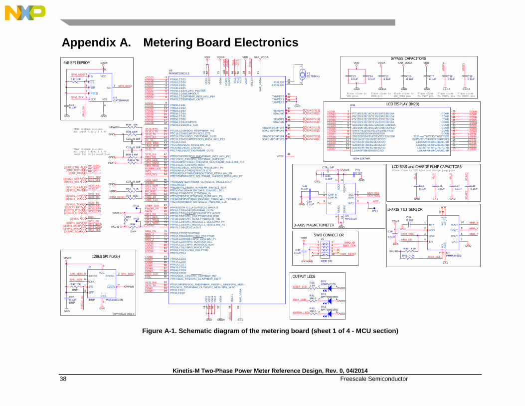
Kinetis-M Two-Phase Power Meter Reference Design, Rev. 0, 04/2014
38 Freescale Semiconductor
Appendix A. Metering Board Electronics
Figure A-1. Schematic diagram of the metering board (sheet 1 of 4 - MCU section)
GND
GND
W25X10CLSN
U8
DNP
CS1
DO/IO12
WP3
GND
4
DI/IO05
CLK6
HOLD7
VCC
8
CAT25040VEU4
CS1
SO2
WP3
VSS
4
SI5
SCK6
HOLD7
VCC
8
Place close toSAR_VDDA pin
Place close to VDDA pin
Place closeto VREFH pin
Place closeto VBAT pin
VC
AP
1
GNDA
VDDA
C24 0.1UF
OPTIONAL ONLY
VLL1
VC
AP
2
VLL2
VLL3
VLL2
VLL1
C23 0.1UF
GND
KWH_LED
I2C0_SDA
I2C0_SCL
VLL3
GND
VPWR
C22 0.1UF RF_IO
VC
AP
2V
CA
P1
R570
C280.1UF
U5PKM34Z128CLL5
PTA0/LCD231
PTA1/LCD242
PTA2/LCD253
PTA3/LCD264
PTA4/LCD27/LLWU_P15/NMI5
PTA5/LCD28/CMP0OUT6
PTA6/LCD29/PXBAR_IN0/LLWU_P147
PTA7/LCD30/PXBAR_OUT08
PTB0/LCD319
VD
D1
10
VS
S1
11
PTB1/LCD3212
PTB2/LCD3313
PTB3/LCD3414
PTB4/LCD3515
PTB5/LCD3616
PTB6/LCD37/CMP1P017
PTB7/LCD38/AFE_CLK18
PTC0/LCD39/SCI3_RTS/PXBAR_IN119
PTC1/LCD40/CMP1P1/SCI3_CTS20
PTC2/LCD41/SCI3_TXD/PXBAR_OUT121
PTC3/LCD42/CMP0P3/SCI3_RXD/LLWU_P1322
PTC4/LCD4323
EXTAL32K26V
DD
A31
VS
SA
32
PTC5/AD0/SCI0_RTS/LLWU_P1244
PTC6/AD1/SCI0_CTS/QT145
PTC7/AD2/SCI0_TXD/PXBAR_OUT246
PTD0/CMP0P0/SCI0_RXD/PXBAR_IN2/LLWU_P1147
PTD1/SCI1_TXD/SPI0_SS/PXBAR_OUT3/QT348
PTD2/CMP0P1/SCI1_RXD/SPI0_SCK/PXBAR_IN3/LLWU_P1049
PTD3/SCI1_CTS/SPI0_MOSI50
PTD4/AD3/SCI1_RTS/SPI0_MISO/LLWU_P951
PTD5/AD4/LPTIM2/QT0/SCI3_CTS52
PTD6/AD5/LPTIM1/CMP1OUT/SCI3_RTS/LLWU_P853
PTD7/CMP0P4/I2C0_SCL/PXBAR_IN4/SCI3_RXD/LLWU_P754
PTE0/I2C0_SDA/PXBAR_OUT4/SCI3_TXD/CLKOUT55
PTE1/RESET56
PTE2/EXTAL1/EWM_IN/PXBAR_IN6/I2C1_SDA57
PTE3/XTAL1/EWM_OUT/AFE_CLK/I2C1_SCL58
VS
S3
59
SA
R_
VS
SA
60
SA
R_
VD
DA
61
VD
D2
62
PTE4/LPTIM0/SCI2_CTS/EWM_IN63
PTE5/QT3/SCI2_RTS/EWM_OUT/LLWU_P664
PTE6/CMP0P2/PXBAR_IN5/SCI2_RXD/LLWU_P5/SWD_IO65
PTE7/AD6/PXBAR_OUT5/SCI2_TXD/SWD_CLK66
PTF0/AD7/RTCCLKOUT/QT2/CMP0OUT67
PTF1/LCD0/AD8/QT0/PXBAR_OUT668
PTF2/LCD1/AD9/CMP1OUT/RTCCLKOUT69
PTF3/LCD2/SPI1_SS/LPTIM1/SCI0_RXD70
PTF4/LCD3/SPI1_SCK/LPTIM0/SCI0_TXD71
PTF5/LCD4/SPI1_MISO/I2C1_SCL/LLWU_P472
PTF6/LCD5/SPI1_MOSI/I2C1_SDA/LLWU_P373
PTF7/LCD6/QT2/CLKOUT74
PTG0/LCD7/QT1/LPTIM275
PTG1/LCD8/AD10/LLWU_P2/LPTIM076
PTG2/LCD9/AD11/SPI0_SS/LLWU_P177
PTG3/LCD10/SPI0_SCK/I2C0_SCL78
PTG4/LCD11/SPI0_MOSI/I2C0_SDA79
PTG5/LCD12/SPI0_MISO/LPTIM180
PTG6/LCD13/LLWU_P0/LPTIM281
PTG7/LCD1482
PTH0/LCD1583
PTH1/LCD1684
PTH2/LCD1785
PTH3/LCD1886
PTH4/LCD1987
PTH5/LCD2088
PTH6/SCI1_CTS/SPI1_SS/PXBAR_IN789
PTH7/SCI1_RTS/SPI1_SCK/PXBAR_OUT790
PTI0/CMP0P5/SCI1_RXD/PXBAR_IN8/SPI1_MISO/SPI1_MOSI91
PTI1/SCI1_TXD/PXBAR_OUT8/SPI1_MOSI/SPI1_MISO92
PTI2/LCD2193
PTI3/LCD2294
VS
S4
95
VLL3
96
VLL2
97
VLL1
98
VC
AP
299
VC
AP
1100
VS
S2
27
TAMPER030
TAMPER129
TAMPER228
VB
AT
24
XTAL32K25
SDADP033
SDADM034
SDADP135
SDADM136
VR
EF
H37
VR
EF
L38
SDADP2/CMP1P239
SDADM2/CMP1P340
VREF41
SDADP3/CMP1P442
SDADM3/CMP1P543
C270.1UF
C260.1UF
R58
0DNP
C250.1UF
Place closeto VREFL pin
GNDA
C190.1UF
RF_CTRL[2]
VR
EF
H
VR
EF
H
RF_CTRL
VR
EF
L
VR
EF
L
C180.1UF
R38 330K
TP13
C170.1UF
VAUX2
R40 4.7M
SWD_CLK
SWD_RESET
SWD_IO
C320.1UF
C160.1UF
VDD
GND
J5
HDR 2X5
1 23 4
657 89 10
SWD CONNECTOR
GND
C150.1UF
D13WP7104LSRD
AC
C140.1UF
D14WP7104LSRD
AC
R41390.0
Y132.768KHz
12
R43390.0
VDD
KVARH_LED
KWH_LED
VDD
OUTPUT LEDS
VDD
R47 10K
DNP
C130.1UFR37 10K
VDD VDDA
C210.1UF
SAR_VDDA
LCD11
MMA_Y
MMA_X
MMA_ZMMA_X
MMA_ZMMA_Y
GND
SPI0_SS
INT1KVARH_LED
C370.1UFDNP
GND
GND
GND
VDD
SAR_VDDA
/RESET
GND
VPWR
GNDA
EOC[2]EOC
I2C1_SCL[2]I2C1_SCLI2C1_SDA[2]I2C1_SDA
SCI3_TX[2]SCI3_RX[2]
SCI3_TXSCI3_RX
SCI3_RTS[2]SCI3_CTS[2]
SCI3_RTS
LCD DISPLAY (8x20)
SCI3_CTS
SCI1_TX[2]SWD_RESETSCI1_RX[2] SCI1_TX
SCI1_RX
SCI0_TX[2]SCI0_RX[2] SCI0_TX
SCI0_RX
RF_IO[2]RF_RST[2] RF_IO
4kB SPI EEPROM
128kB SPI FLASH
RF_RST
SPI1_SCK[2]
SPI1_SS[2]SPI1_MOSI[2]
TP12
SPI1_MISO[2]
VPWR
SPI1_SS
SPI1_SCKSPI1_MISOSPI1_MOSI
SPI1_SCK
SPI1_MOSI SPI1_MISO
GND
FLASH_SS
EOC
MMA_EN
VBAT
GND
GND
U7PMMA8491Q
BYP1
NC
_1
111
GN
D6
VDD2
EN4
XOUT10
ZOUT8
NC
_1
212
YOUT9
SC
L5
SDA3
GND7
GND
I2C0_SCLR46 4.7K
MMA_EN
GND
C340.1UF
R45 4.7K
DS1
GDH-1247WP
P7/14D/14E/14C/14G/14F/14B/14A1
P6/13D/13E/13C/13G/13F/13B/13A2
P5/12D/12E/12C/12G/12F/12B/12A3
P4/11D/11E/11C/11G/11F/11B/11A4
S18/10D/10E/10C/10G/10F/10B/10A5
15D/15E/15C/15G/15F/15B/15A/S176
S40/S7/S12/S13/S11/S10/S14/S197
S3/S4/S8/S5/S9/S6/S1/S208
S28/S25/S24/S16/S23/S22/S21/S389
S26/1A/1F/1B/1G/1E/1C/1D10
S27/2A/2F/2B/2G/2E/2C/2D11
S39/3A/3F/3B/3G/3E/3C/3D12
S36/4A/4F/4B/4G/4E/4C/4D13
L1/5A/5F/5B/5G/5E/5C/5D14
COM828
COM727
COM626
COM525
COM424
COM323
COM222
COM121
S15/rms/T1/T2/T3/T4/S37/S3520
S2/P3/S31/S32/S33/S34/P2/P119
S30/9A/9F/9B/9G/9E/9C/9D18
S29/8A/8F/8B/8G/8E/8C/8D17
L3/7A/7F/7B/7G/7E/7C/7D16
L2/6A/6F/6B/6G/6E/6C/6D15
SCI1_TX
COM3COM2COM1
SCI1_RX
COM6
LCD37LCD38
COM8COM7
LCD33LCD34LCD35LCD36
LCD11
LCD14LCD13LCD12
LCD25LCD24LCD23
LCD29LCD28LCD27LCD26
LCD32LCD31LCD30
COM4COM5
VAUX
VAUX
VAUX
RF_CTRLRF_RST
R42 4.7K
SPI1_MOSISPI1_MISOSPI1_SCK
C36
0.1UF
SPI1_SS
I2C1_SCLI2C1_SDA
R36 47K
GND
VPWR voltage divider: ADC input 3.151V @ 3.6V
SPI0_MISOSPI0_MOSISPI0_SCK
SCI0_RX
SDADP0[1]
SCI0_TX
R39 1.6M
VBAT_MSR
SDADP1[1]
SDADM0[1]
SDADM1[1]
SDADP2[1]SDADM2[1]
SDADP3[1]SDADM3[1]
VBAT voltage divider:
ADC input 0.838V @ 3.3V
(wait for 2s to stabilize)
VAUX
R44 820
PWR_MSR
FL
AS
H_
SS
I2C0_SDA
3-AXIS TILT SENSOR
GND
U6MAG3110
CAP_A1
VD
D2
NC3
CAP_R4
GN
D1
5
SDA6SCL7V
DD
IO8
INT19
GN
D2
10
I2C0_SCLI2C0_SDA
C300.1UF
C330.1UF
C350.1UFGND
GND
GND
C310.1UF
VAUX
GND
SPI0_MOSI
C29 1uF
INT1
SPI0_SCK
SPI0_MISO
VAUX
COM6COM7COM8
COM2
COM3COM4COM5
COM1
GND LCD36LCD37LCD38
LCD32LCD33LCD34LCD35
LCD31
LCD27LCD28LCD29LCD30
LCD23LCD24LCD25LCD26
SCI3_RTSSCI3_CTS
VDD
GND
SCI3_RX
LCD12LCD13LCD14
SCI3_TX
GNDA
SWD_IOSWD_CLK
D21HSMS-C170
AC
CLKOUT
R553.9K
VDDUSER_LED
SP
I0_
SS
3-AXIS MAGNETOMETER
BYPASS CAPACITORS
USER_LED
TP11
VDD
GND
GND
Place close toVDD pins
LCD BIAS and CHARGE PUMP CAPACITORSPlace close to LCD bias and charge pump pins
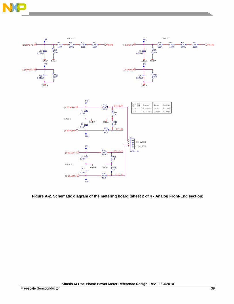
Kinetis-M One-Phase Power Meter Reference Design, Rev. 0, 04/2014
Freescale Semiconductor 39
Figure A-2. Schematic diagram of the metering board (sheet 2 of 4 - Analog Front-End section)
R9390
R13390
R8390
R12390
C20.012uF
C40.012uF
GNDA GNDA
GNDA
C10.012uF
C30.012uF
GNDA
GNDA
GNDA
L1[4]L2[4]
PHASE 1PHASE 2
R1
150K
R2
150K
R3
150K
SDADM2[3]
R4
150KSDADP2[3]SDADP3[3]
SDADM3[3]
R10
150K
R7
150K
R5
150K
R6
150K
TP1
TP2
TP3
TP4
R151.5
R211.5
R181.5
R241.5
C6
0.1UF
TP6
Sensor Mains ScalingR15,R18
R21,R24
1.5 CT 1:2000 U.S. 235 Amps
5.6 CT 1:2000 Japan 63 Amps
TP8
C8
0.1UF
J1
HDR 1X4
1234
R19
47.0
R14
47.0
CT1=1:2000
GNDA
CT1_OUT
C50.1UF
GNDA
CT1_IN
CT2_IN
CT2_OUT
GNDA
PHASE 1
R25
47.0
R20
47.0
GNDA
C70.1UF
CT2=1:2000
PHASE 2
SDADP1[3]
SDADM1[3]
SDADM0[3]
SDADP0[3]
TP5
TP7
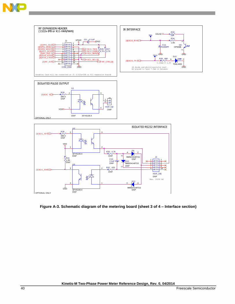
Kinetis-M Two-Phase Power Meter Reference Design, Rev. 0, 04/2014
40 Freescale Semiconductor
Figure A-3. Schematic diagram of the metering board (sheet 3 of 4 – Interface section)
J2
CON_2X10
1 23 4
657 89 10
11 1213 1415 1617 1819 20
Daughter Card will be connected on J2 (1322x-IPB or K11 expansion board)
OPTIONAL ONLY
OPTIONAL ONLY
SCI1_TX[3]
SCI1_RX[3]
EOC[3]
SCI3_TX[3]SCI3_RX[3]
RF_CTRL[3]RF_IO[3]
SCI3_RTS[3]SCI3_CTS[3]
RF_RST[3]SPI1_SCK[3]
SPI1_MOSI[3]
I2C1_SCL[3]
I2C1_SDA[3]
C112200PF
R33
10K
SCI0_TX[3]
SCI0_RX[3]
GND
GND
IR INTERFACE
GND
~2.65mA @ 3.3V
R35 680
TP10
TP9
IR diode and phototransistor mustbe placed to have 7.5mm in between
D12
TSAL4400
A C
Q1OP506B
21
R34
1.0K
VAUX2
C9 0.1UF
J3
HDR 1X2
DNP
12
D10MMSD4148T1G
DNP
AC
R32 470
DNP
D11
MMSD4148T1GDNP
AC
J4
HDR_2X5
DNP
1 23 4
657 89 10
VDD
U2
SFH6106-4DNP
1
2 3
4
U3
SFH6106-4DNP
1
23
4
U1
SFH6106-4DNP
1
2 3
4
R28
390.0DNP
R311.0KDNP
R29
390.0DNP
VDD
ISOLATED RS232 INTERFACE
ISOLATED PULSE OUTPUT
GND
R274.7K
R264.7K
R30 4.7K
DNP
D9
MMSD4148T1GDNP
A C
GND
VPWRGND
C102.2uFDNP
Max. 19200 Bd
RF EXPANSION HEADER(1322x-IPB or K11-HAN/NAN)
SPI1_SS[3]
SPI1_MISO[3]
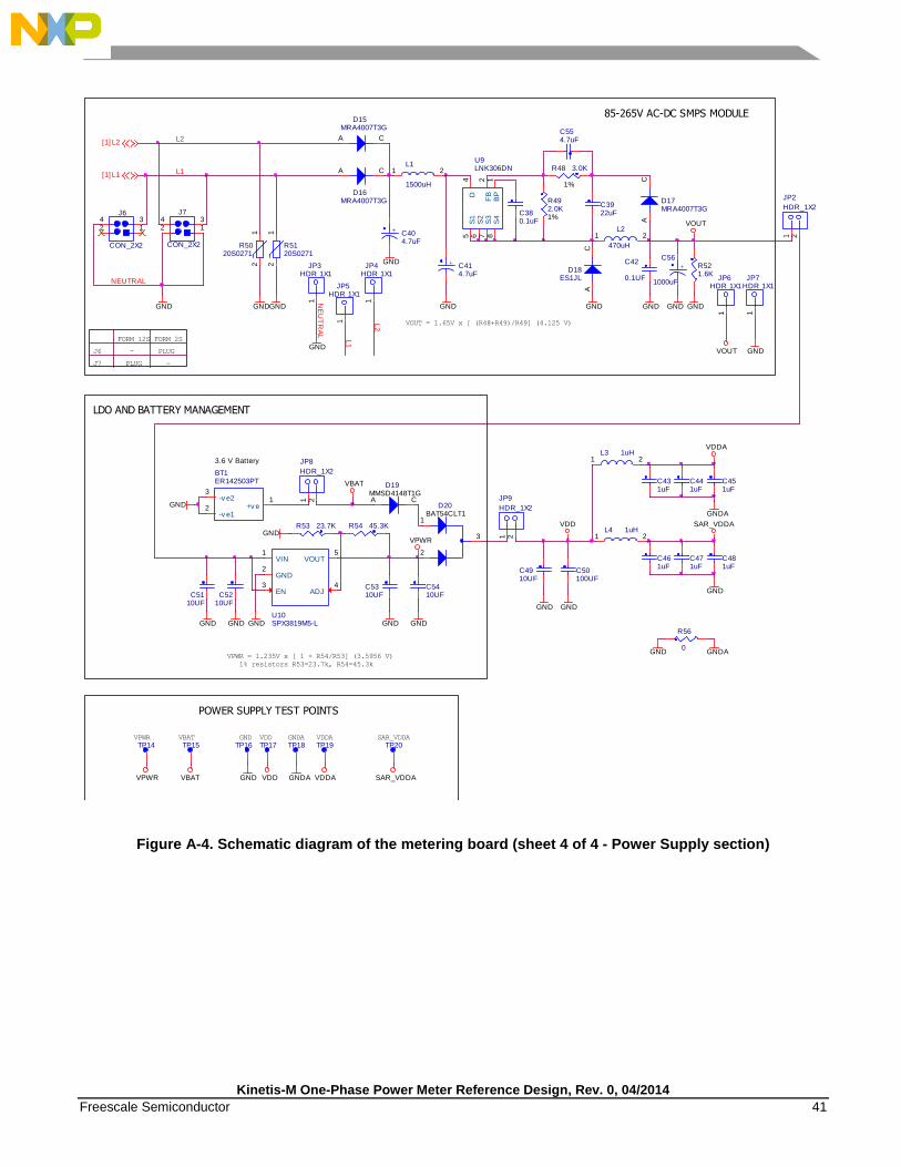
Kinetis-M One-Phase Power Meter Reference Design, Rev. 0, 04/2014
Freescale Semiconductor 41
Figure A-4. Schematic diagram of the metering board (sheet 4 of 4 - Power Supply section)
GND
L1[1]
R5020S0271
12
L2[1]
J6
CON_2X2
1234
R5120S0271
12
J7
CON_2X2
1234
GND
JP6HDR 1X1
1
JP7HDR 1X1
1
GND
D19MMSD4148T1GA C
U10SPX3819M5-L
EN3
VIN1
GND2
ADJ4
VOUT5
R53 23.7KGND
GND
NE
UT
RA
L
L3 1uH1 2
C5110UF
L4 1uH1 2
85-265V AC-DC SMPS MODULE
L1
GNDA
GND
R492.0K
1%
1%
R48 3.0K
D16MRA4007T3G
A C
+
C56
1000uF
D17MRA4007T3G
AC
C3922uF
D18ES1JL
AC
GND
+ C404.7uF
VDDA
+ C414.7uF
R54 45.3K
GND
GND
SAR_VDDA
C451uF
C441uF
C431uF
C481uF
C471uF
C461uF
GND
GND
GNDA
VBAT
VOUT
VOUT
GND
VDD
GND
GNDGND
C4910UF
GND GND
C5410UFC52
10UF
VPWR = 1.235V x [ 1 + R54/R53] (3.5956 V)
GND
C5310UF
GND
D15MRA4007T3G
A C
C380.1uF
1% resistors R53=23.7k, R54=45.3k
GND
VOUT = 1.65V x [ (R48+R49)/R49] (4.125 V)
L2
JP2
HDR_1X2
1 2
JP8
HDR_1X2
1 2
JP4HDR 1X1
1
GND
L2
JP9
HDR_1X21 2
L1
1500uH
1 2
VPWR
BT1ER142503PT
+v e1-v e2
3
-v e12
3.6 V Battery
R521.6K
JP3HDR 1X1
1GND
JP5HDR 1X1
1
D20BAT54CLT1
2
3
1
TP19
R56
0
TP16GNDA
GNDVBATVPWR
TP15VBATVPWR
VDD
VDDGND
TP17VDDA SAR_VDDA
VDDA
TP20
SAR_VDDAGNDA
TP18TP14
POWER SUPPLY TEST POINTS
NEUTRAL
PLUG
PLUG
L1
C554.7uF
FORM 2SFORM 12S
J6
J7
-
-
L2
470uH
1 2
LDO AND BATTERY MANAGEMENT
U9LNK306DN
BP
1F
B2
D4
S1
5
S2
6
S3
7
S4
8
C50100UF
C42
0.1UF
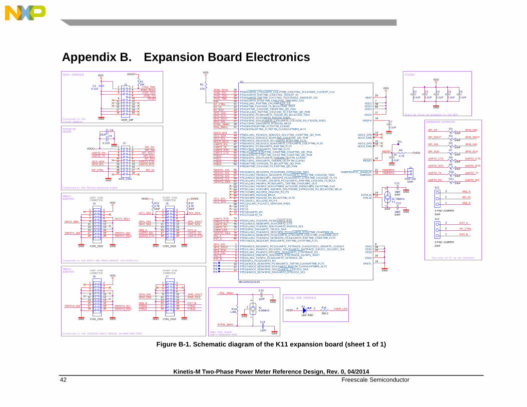
Kinetis-M Two-Phase Power Meter Reference Design, Rev. 0, 04/2014
42 Freescale Semiconductor
Appendix B. Expansion Board Electronics
Figure B-1. Schematic diagram of the K11 expansion board (sheet 1 of 1)
OPTICAL USER INTERFACE
R15
390.0
R2
47K
R110K
MK11DN512VLK5
U1
PTE16/ADC0_SE4A/SPI0_PCS0/UART2_TX/FTM_CLKIN0/FTM0_FLT39
PTE19/ADC0_SE7A/SPI0_SIN/UART2_RTS/I2C0_SCL12
PTE1/LLWU_P0/ADC0_SE11/SPI1_SOUT/UART1_RX/TRACE_D3/I2C1_SCL/SPI1_SIN2
PTB1/ADC0_SE9/I2C0_SDA/FTM1_CH1/FTM1_QD_PHB44
PTB10/SPI1_PCS0/UART3_RX/FTM0_FLT147 PTB3/ADC0_SE13/I2C0_SDA/UART0_CTS/UART0_COL/FTM0_FLT046
PTC0/ADC0_SE14/SPI0_PCS4/PDB0_EXTRG/I2S0_TXD155
PTC1/LLWU_P6/ADC0_SE15/SPI0_PCS3/UART1_RTS/FTM0_CH0/I2S0_TXD056
PTD0/LLWU_P12/SPI0_PCS0/UART2_RTS73
PTD4/LLWU_P14/ADC0_SE21/SPI0_PCS1/UART0_RTS/FTM0_CH4/EWM_IN77
PTD5/ADC0_SE6B/SPI0_PCS2/UART0_CTS/UART0_COL/FTM0_CH5/EWM_OUT78
PTA5/FTM0_CH2/I2S0_TX_BCLK/JTAG_TRST31
PTB0/LLWU_P5/ADC0_SE8/I2C0_SCL/FTM1_CH0/FTM1_QD_PHA43
PTB11/SPI1_SCK/UART3_TX/FTM0_FLT248
PTB12/UART3_RTS/FTM1_CH0/FTM0_CH4/FTM1_QD_PHA49
PTD7/ADC0_SE22/CMT_IRO/UART0_TX/FTM0_CH7/FTM0_FLT180
PTC17/UART3_TX72
PTE0/ADC0_SE10/SPI1_PCS1/UART1_TX/TRACE_CLKOUT/I2C1_SDA/RTC_CLKOUT1
PTC1370
PTC16/UART3_RX71
PTC10/I2C1_SCL/I2S0_RX_FS67
PTA15/SPI0_SCK/UART0_RX/I2S0_RXD035
PTA16/SPI0_SOUT/UART0_CTS/UART0_COL/I2S0_RX_FS/I2S0_RXD136
VSS359
VSSA20
EXTAL3224
PTA0/UART0_CTS/UART0_COL/FTM0_CH5/JTAG_TCLK/SWD_CLK/EZP_CLK26
PTA1/UART0_RX/FTM0_CH6/JTAG_TDI/EZP_DI27
PTA12/FTM1_CH0/I2S0_TXD0/FTM1_QD_PHA32
PTA13/LLWU_P4/FTM1_CH1/I2S0_TX_FS/FTM1_QD_PHB33
PTA17/SPI0_SIN/UART0_RTS/I2S0_MCLK37
PTA18/EXTAL0/FTM0_FLT2/FTM_CLKIN040
PTA19/XTAL0/FTM1_FLT0/FTM_CLKIN1/LPTMR0_ALT141
PTA14/SPI0_PCS0/UART0_TX/I2S0_RX_BCLK/I2S0_TXD134
PTB17/SPI1_SIN/UART0_TX/EWM_OUT/FTM_CLKIN152
PTB18/FTM2_CH0/I2S0_TX_BCLK/FTM2_QD_PHA53
PTB19/FTM2_CH1/I2S0_TX_FS/FTM2_QD_PHB54
PTB2/ADC0_SE12/I2C0_SCL/UART0_RTS/FTM0_FLT345
PTC11/LLWU_P11/I2C1_SDA/I2S0_RXD168
PTC1269
PTC9/CMP0_IN3/I2S0_RX_BCLK/FTM2_FLT066
PTD1/ADC0_SE5B/SPI0_SCK/UART2_CTS74
PTD2/LLWU_P13/SPI0_SOUT/UART2_RX/I2C0_SCL75
PTD3/SPI0_SIN/UART2_TX/I2C0_SDA76
PTD6/LLWU_P15/ADC0_SE7B/SPI0_PCS3/UART0_RX/FTM0_CH6/FTM0_FLT079
PTE17/ADC0_SE5A/SPI0_SCK/UART2_RX/FTM_CLKIN1/LPTMR0_ALT310
PTE18/ADC0_SE6A/SPI0_SOUT/UART2_CTS/I2C0_SDA11
VDD360
VBAT25
VDD17
PTB16/SPI1_SOUT/UART0_RX/EWM_IN/FTM_CLKIN051
VDD238
VDDA17
TAMPER122
VSS239
VREFH18
VREFL19
VSS18
PTB13/UART3_CTS/FTM1_CH1/FTM0_CH5/FTM1_QD_PHB50
XTAL3223
RESET42
TAMPER0/RTC_WAKEUP21
PTA2/UART0_TX/FTM0_CH7/JTAG_TDO/TRACE_SWO/EZP_DO28
PTA3/UART0_RTS/FTM0_CH0/JTAG_TMS/SWD_DIO29
PTA4/LLWU_P3/FTM0_CH1/NMI/EZP_CS30
PTC2/ADC0_SE4B/CMP1_IN0/SPI0_PCS2/UART1_CTS/FTM0_CH1/I2S0_TX_FS57
PTC3/LLWU_P7/CMP1_IN1/SPI0_PCS1/UART1_RX/FTM0_CH2/I2S0_TX_BCLK58
PTC4/LLWU_P8/SPI0_PCS0/UART1_TX/FTM0_CH3/CMP1_OUT61
PTC5/LLWU_P9/SPI0_SCK/LPTMR0_ALT2/I2S0_RXD0/CMP0_OUT/FTM0_CH262
PTC6/LLWU_P10/CMP0_IN0/SPI0_SOUT/PDB0_EXTRG/I2S0_RX_BCLK/I2S0_MCLK63
PTC7/CMP0_IN1/SPI0_SIN/I2S0_RX_FS64
PTC8/CMP0_IN2/I2S0_MCLK65
PTE2/LLWU_P1/ADC0_DP1/SPI1_SCK/UART1_CTS/TRACE_D23
PTE3/ADC0_DM1/SPI1_SIN/UART1_RTS/TRACE_D1/SPI1_SOUT4
PTE4/LLWU_P2/SPI1_PCS0/UART3_TX/TRACE_D05
PTE5/SPI1_PCS2/UART3_RX6
ADC0_DP013
ADC0_DM014
ADC0_DP315
ADC0_DM316
J1
HDR_19P
1 23 4
658
9 1011 1213 1415 1617 1819 20
D1
LED RED
A C
C12
18pFDNP
SJ1
3 PAD JUMPER
DNP
1
2
3
SJ2
3 PAD JUMPER
DNP
1
2
3
C11
18pFDNP
IRQ_B
RF_IO
RST_B
RF_CTRL
RST_A
IRQ_A
R4
0 DNPR5
0 DNPR7
0 DNPR8
0 DNPR9
0 DNPR10
0 DNPR11
0 DNP
I2C1_SCLI2C1_SDA
JTAG_TCLKJTAG_TDI
JTAG_TMSJTAG_TDO
C13
12PF
C14
12PF
R141.0M
XTAL_8MHz
GND
GND
EXTAL_8MHz
GND
8MHz XTAL BLOCK
DON'T POPULATE PART
VDD
XTAL_8MHzEXTAL_8MHz
I2C0_SDA
I2C0_SCLI2C0_SDA
I2C0_SCL
GND
JTAG_TDIJTAG_TDO
JTAG_TCLK
RF_CTRLRF_IO
RF_IORF_CTRL
UART3_RTSUART3_CTS
UART3_TX
J7
CON_2X10
1 23 4
657 89 10
11 1213 1415 1617 1819 20
LEFT SIDECONNECTOR
RIGHT SIDECONNECTOR
GND GND
J6
CON_2X10
1 23 4
657 89 10
11 1213 1415 1617 1819 20
UART3_RXUART3_TX
VDD
IRQ_BPTB16PTB18
GND
C8
10UF
GND
SPI0_SS0SPI0_SIN
Connected to the COCONINO RADIO MODULE (X-TRWPI-MC13242)
TWRPI2ADAPTORS
USER_LED
RST_B
SPI0_SCKSPI0_SOUT
PTB19PTB17
TP1
TWRPI2_ID1
TWRPI1_ID1TWRPI1_ID0
TWRPI2_ID1TWRPI2_ID0TWRPI1_ID1TWRPI1_ID0
TWRPI2_RES
UART3_RX
TP2TP3TP4TP5
C7
0.1UF
GND
PTB19PTB18PTB17PTB16
UART2_TXUART2_RXUART2_CTSUART2_RTS
J5
CON_2X10
1 23 4
657 89 10
11 1213 1415 1617 1819 20
DEBUG INTERFACE
EXPANSION
HEADER
SPI_SINSPI_SOUTSPI_SCK
TWRPI2_ID0
RIGHT SIDE
CONNECTOR
LEFT SIDE
CONNECTOR
TWRPI1_RES
ADC0_SE13ADC0_SE8
TWRPI2_RES
Connected to the
J-Link adaptor
Connected to the Photon metering board
ADC0_SE13
ADC0_SE8
GND
J4
CON_2X10
1 23 4
657 89 10
11 1213 1415 1617 1819 20
GND
GND
VDDVDD
RESET
IRQ_BRST_B
FILTERS
VDD
VDD
Place as close as possible to the MCU
R6
4.7K
Y132.768KHz
DNP
12
UART2_CTS
IRQ_AUART2_RX
GND
GND
GND
R134.7KDNP
R124.7KDNP
GND
VDD
VDD
GND
GND
GND
SPI1_SS1SPI1_SIN
Connected to the NIVIS SMO RADIO MODULE (40-00045-01)
TWRPI1
ADAPTORS
VDD
SPI1_SOUT
I2C1_SDA
UART2_RTSUART2_TXRST_A
SPI1_SCK
VDD
C10
0.1UF
RESET
VDD
C2
0.1UF
I2C1_SCL
C3
0.1UF
J2
HDR_2X10
1234
6 57891011121314151617181920
C4
0.1UF
VDD
C5
0.1UF
GND
C6
0.1UF
SPI_SS
INTERFACES BYPASSING
Use only if U1 is not present!
TWRPI1_RESIRQ_ARST_A
USER_LED
NMI
SPI1_SOUTSPI1_SS1
SPI1_SINSPI1_SCK
UART3_RTSUART3_CTS
C9
0.1UF
SPI0_SS0
SPI0_SINSPI0_SOUT
R3
0 DNP
SPI0_SS0SPI_SS
SPI0_SCK
RF_RST
RF_RST
X18.00MHZ
13
2
SPI0_SOUTSPI_SOUT
JTAG_TMS
J3
HDR 1X2DNP
12
SPI0_SINSPI_SIN
SPI0_SCKSPI_SCK
UART2_CTSUART3_CTS
TAMPER0TAMPER1
C10.1UF
UART2_RTSUART3_RTS
UART2_TXUART3_TX
UART2_RXUART3_RX
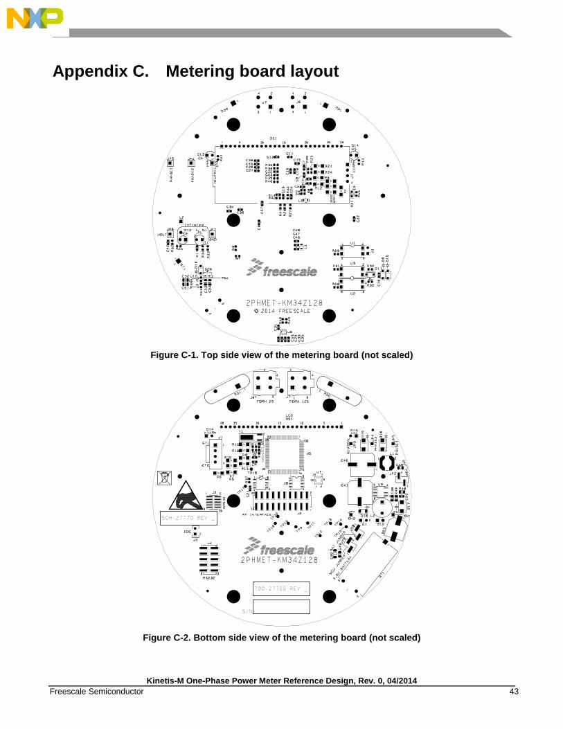
Kinetis-M One-Phase Power Meter Reference Design, Rev. 0, 04/2014
Freescale Semiconductor 43
Appendix C. Metering board layout
Figure C-1. Top side view of the metering board (not scaled)
Figure C-2. Bottom side view of the metering board (not scaled)
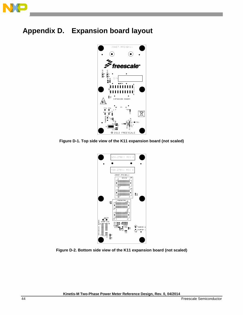
Kinetis-M Two-Phase Power Meter Reference Design, Rev. 0, 04/2014
44 Freescale Semiconductor
Appendix D. Expansion board layout
Figure D-1. Top side view of the K11 expansion board (not scaled)
Figure D-2. Bottom side view of the K11 expansion board (not scaled)
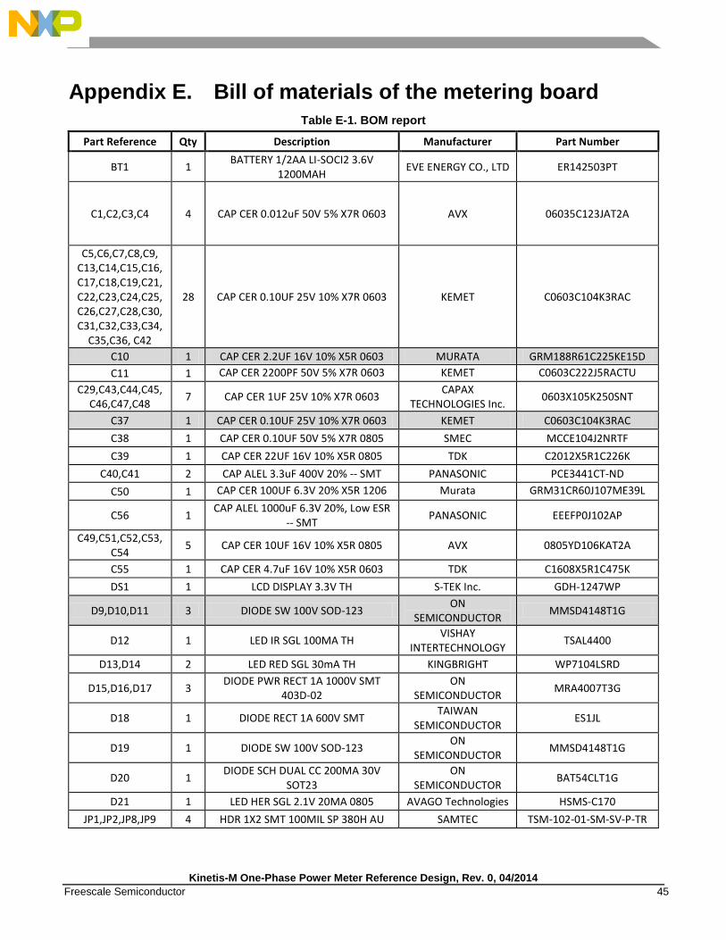
Kinetis-M One-Phase Power Meter Reference Design, Rev. 0, 04/2014
Freescale Semiconductor 45
Appendix E. Bill of materials of the metering board
Table E-1. BOM report
Part Reference Qty Description Manufacturer Part Number
BT1 1 BATTERY 1/2AA LI-SOCI2 3.6V
1200MAH EVE ENERGY CO., LTD ER142503PT
C1,C2,C3,C4 4 CAP CER 0.012uF 50V 5% X7R 0603 AVX 06035C123JAT2A
C5,C6,C7,C8,C9, C13,C14,C15,C16,C17,C18,C19,C21,C22,C23,C24,C25,C26,C27,C28,C30,C31,C32,C33,C34,
C35,C36, C42
28 CAP CER 0.10UF 25V 10% X7R 0603 KEMET C0603C104K3RAC
C10 1 CAP CER 2.2UF 16V 10% X5R 0603 MURATA GRM188R61C225KE15D
C11 1 CAP CER 2200PF 50V 5% X7R 0603
KEMET
C0603C222J5RACTU C29,C43,C44,C45,
C46,C47,C48 7 CAP CER 1UF 25V 10% X7R 0603
CAPAX TECHNOLOGIES Inc.
0603X105K250SNT
C37 1 CAP CER 0.10UF 25V 10% X7R 0603 KEMET C0603C104K3RAC
C38 1 CAP CER 0.10UF 50V 5% X7R 0805 SMEC MCCE104J2NRTF
C39 1 CAP CER 22UF 16V 10% X5R 0805 TDK C2012X5R1C226K
C40,C41 2 CAP ALEL 3.3uF 400V 20% -- SMT PANASONIC PCE3441CT-ND
C50 1 CAP CER 100UF 6.3V 20% X5R 1206 Murata GRM31CR60J107ME39L
C56 1 CAP ALEL 1000uF 6.3V 20%, Low ESR
-- SMT PANASONIC EEEFP0J102AP
C49,C51,C52,C53,C54
5 CAP CER 10UF 16V 10% X5R 0805 AVX 0805YD106KAT2A
C55 1 CAP CER 4.7uF 16V 10% X5R 0603 TDK C1608X5R1C475K
DS1 1 LCD DISPLAY 3.3V TH S-TEK Inc. GDH-1247WP
D9,D10,D11 3 DIODE SW 100V SOD-123 ON
SEMICONDUCTOR MMSD4148T1G
D12 1 LED IR SGL 100MA TH VISHAY
INTERTECHNOLOGY TSAL4400
D13,D14 2 LED RED SGL 30mA TH KINGBRIGHT WP7104LSRD
D15,D16,D17 3 DIODE PWR RECT 1A 1000V SMT
403D-02 ON
SEMICONDUCTOR MRA4007T3G
D18 1 DIODE RECT 1A 600V SMT TAIWAN
SEMICONDUCTOR ES1JL
D19 1 DIODE SW 100V SOD-123 ON
SEMICONDUCTOR MMSD4148T1G
D20 1 DIODE SCH DUAL CC 200MA 30V
SOT23 ON
SEMICONDUCTOR BAT54CLT1G
D21 1 LED HER SGL 2.1V 20MA 0805 AVAGO Technologies HSMS-C170
JP1,JP2,JP8,JP9 4 HDR 1X2 SMT 100MIL SP 380H AU SAMTEC TSM-102-01-SM-SV-P-TR
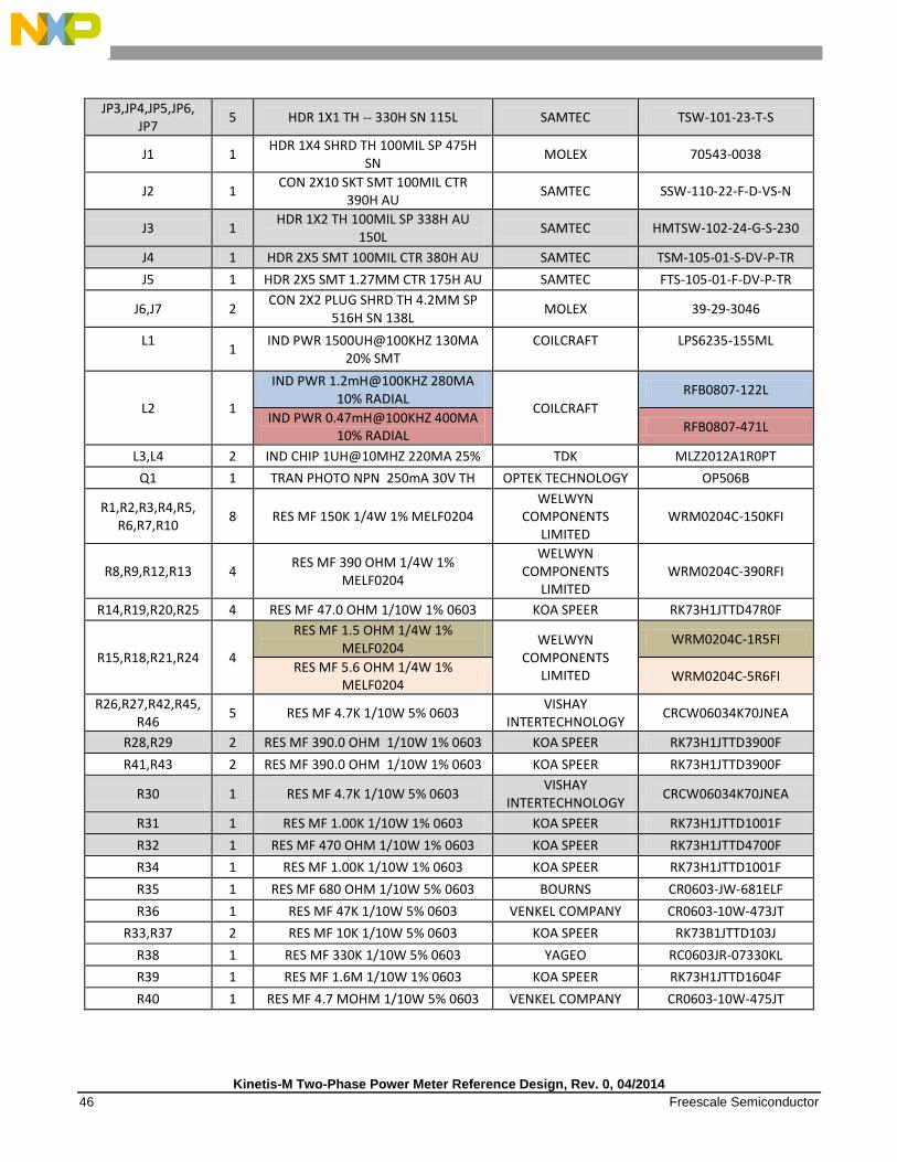
Kinetis-M Two-Phase Power Meter Reference Design, Rev. 0, 04/2014
46 Freescale Semiconductor
JP3,JP4,JP5,JP6, JP7
5 HDR 1X1 TH -- 330H SN 115L SAMTEC TSW-101-23-T-S
J1 1 HDR 1X4 SHRD TH 100MIL SP 475H
SN MOLEX 70543-0038
J2 1 CON 2X10 SKT SMT 100MIL CTR
390H AU SAMTEC SSW-110-22-F-D-VS-N
J3 1 HDR 1X2 TH 100MIL SP 338H AU
150L SAMTEC HMTSW-102-24-G-S-230
J4 1 HDR 2X5 SMT 100MIL CTR 380H AU SAMTEC TSM-105-01-S-DV-P-TR
J5 1 HDR 2X5 SMT 1.27MM CTR 175H AU SAMTEC FTS-105-01-F-DV-P-TR
J6,J7 2 CON 2X2 PLUG SHRD TH 4.2MM SP
516H SN 138L MOLEX 39-29-3046
L1
1 IND PWR 1500UH@100KHZ 130MA
20% SMT COILCRAFT
LPS6235-155ML
L2 1
IND PWR 1.2mH@100KHZ 280MA 10% RADIAL
COILCRAFT
RFB0807-122L
IND PWR 0.47mH@100KHZ 400MA 10% RADIAL
RFB0807-471L
L3,L4 2 IND CHIP 1UH@10MHZ 220MA 25% TDK MLZ2012A1R0PT
Q1 1 TRAN PHOTO NPN 250mA 30V TH OPTEK TECHNOLOGY OP506B
R1,R2,R3,R4,R5, R6,R7,R10
8 RES MF 150K 1/4W 1% MELF0204 WELWYN
COMPONENTS LIMITED
WRM0204C-150KFI
R8,R9,R12,R13 4 RES MF 390 OHM 1/4W 1%
MELF0204
WELWYN COMPONENTS
LIMITED WRM0204C-390RFI
R14,R19,R20,R25 4 RES MF 47.0 OHM 1/10W 1% 0603 KOA SPEER RK73H1JTTD47R0F
R15,R18,R21,R24 4
RES MF 1.5 OHM 1/4W 1% MELF0204
WELWYN COMPONENTS
LIMITED
WRM0204C-1R5FI
RES MF 5.6 OHM 1/4W 1% MELF0204
WRM0204C-5R6FI
R26,R27,R42,R45,R46
5 RES MF 4.7K 1/10W 5% 0603 VISHAY
INTERTECHNOLOGY CRCW06034K70JNEA
R28,R29 2 RES MF 390.0 OHM 1/10W 1% 0603 KOA SPEER RK73H1JTTD3900F
R41,R43 2 RES MF 390.0 OHM 1/10W 1% 0603 KOA SPEER RK73H1JTTD3900F
R30 1 RES MF 4.7K 1/10W 5% 0603 VISHAY
INTERTECHNOLOGY CRCW06034K70JNEA
R31 1 RES MF 1.00K 1/10W 1% 0603 KOA SPEER RK73H1JTTD1001F
R32 1 RES MF 470 OHM 1/10W 1% 0603 KOA SPEER RK73H1JTTD4700F
R34 1 RES MF 1.00K 1/10W 1% 0603 KOA SPEER RK73H1JTTD1001F
R35 1 RES MF 680 OHM 1/10W 5% 0603 BOURNS CR0603-JW-681ELF
R36 1 RES MF 47K 1/10W 5% 0603 VENKEL COMPANY CR0603-10W-473JT
R33,R37 2 RES MF 10K 1/10W 5% 0603 KOA SPEER RK73B1JTTD103J
R38 1 RES MF 330K 1/10W 5% 0603 YAGEO RC0603JR-07330KL
R39 1 RES MF 1.6M 1/10W 1% 0603 KOA SPEER RK73H1JTTD1604F
R40 1 RES MF 4.7 MOHM 1/10W 5% 0603 VENKEL COMPANY CR0603-10W-475JT
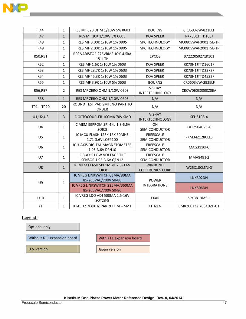
Kinetis-M One-Phase Power Meter Reference Design, Rev. 0, 04/2014
Freescale Semiconductor 47
R44 1 RES MF 820 OHM 1/10W 5% 0603 BOURNS CR0603-JW-821ELF
R47 1 RES MF 10K 1/10W 5% 0603 KOA SPEER RK73B1JTTD103J
R48 1 RES MF 3.00K 1/10W 1% 0805 SPC TECHNOLOGY MC0805WAF3001T5E-TR
R49 1 RES MF 2.00K 1/10W 1% 0805 SPC TECHNOLOGY MC0805WAF2001T5E-TR
R50,R51 2 RES VARISTOR 275VRMS 10% 4.5kA
151J TH EPCOS B72220S0271K101
R52 1 RES MF 1.6K 1/10W 1% 0603 KOA SPEER RK73H1JTTD1601F
R53 1 RES MF 23.7K 1/10W 1% 0603 KOA SPEER RK73H1JTTD2372F
R54 1 RES MF 45.3K 1/10W 1% 0603 KOA SPEER RK73H1JTTD4532F
R55 1 RES MF 3.9K 1/10W 5% 0603 BOURNS CR0603-JW-392ELF
R56,R57 2 RES MF ZERO OHM 1/10W 0603 VISHAY
INTERTECHNOLOGY CRCW06030000Z0EA
R58 1 RES MF ZERO OHM 1/10W 0603 N/A N/A
TP1….TP20 20 ROUND TEST PAD SMT; NO PART TO
ORDER N/A N/A
U1,U2,U3 3 IC OPTOCOUPLER 100MA 70V SMD VISHAY
INTERTECHNOLOGY SFH6106-4
U4 1 IC MEM EEPROM SPI 4Kb 1.8-5.5V
SOIC8 ON
SEMICONDUCTOR CAT25040VE-G
U5 1 IC MCU FLASH 128K 16K 50MHZ
1.71-3.6V LQFP100 FREESCALE
SEMICONDUCTOR PKM34Z128CLL5
U6 1 IC 3-AXIS DIGITAL MAGNETOMETER
1.95-3.6V DFN10 FREESCALE
SEMICONDUCTOR MAG3110FC
U7 1 IC 3-AXIS LOW VOLTAGE TILT
SENSOR 1.95-3.6V QFN12 FREESCALE
SEMICONDUCTOR MMA8491Q
U8 1 IC MEM FLASH SPI 1MBIT 2.3-3.6V
SOIC8 WINBOND
ELECTRONICS CORP W25X10CLSNIG
U9 1
IC VREG LINKSWITCH 63MA/80MA 85-265VAC/700V S0-8C POWER
INTEGRATIONS
LNK302DN
IC VREG LINKSWITCH 225MA/360MA 85-265VAC/700V S0-8C
LNK306DN
U10 1 IC VREG LDO ADJ 500MA 2.5-16V
SOT23-5 EXAR SPX3819M5-L
Y1 1 XTAL 32.768KHZ PAR 20PPM -- SMT CITIZEN CMR200T32.768KDZF-UT
Legend:
Optional only
Without K11 expansion board With K11 expansion board
U.S. version Japan version
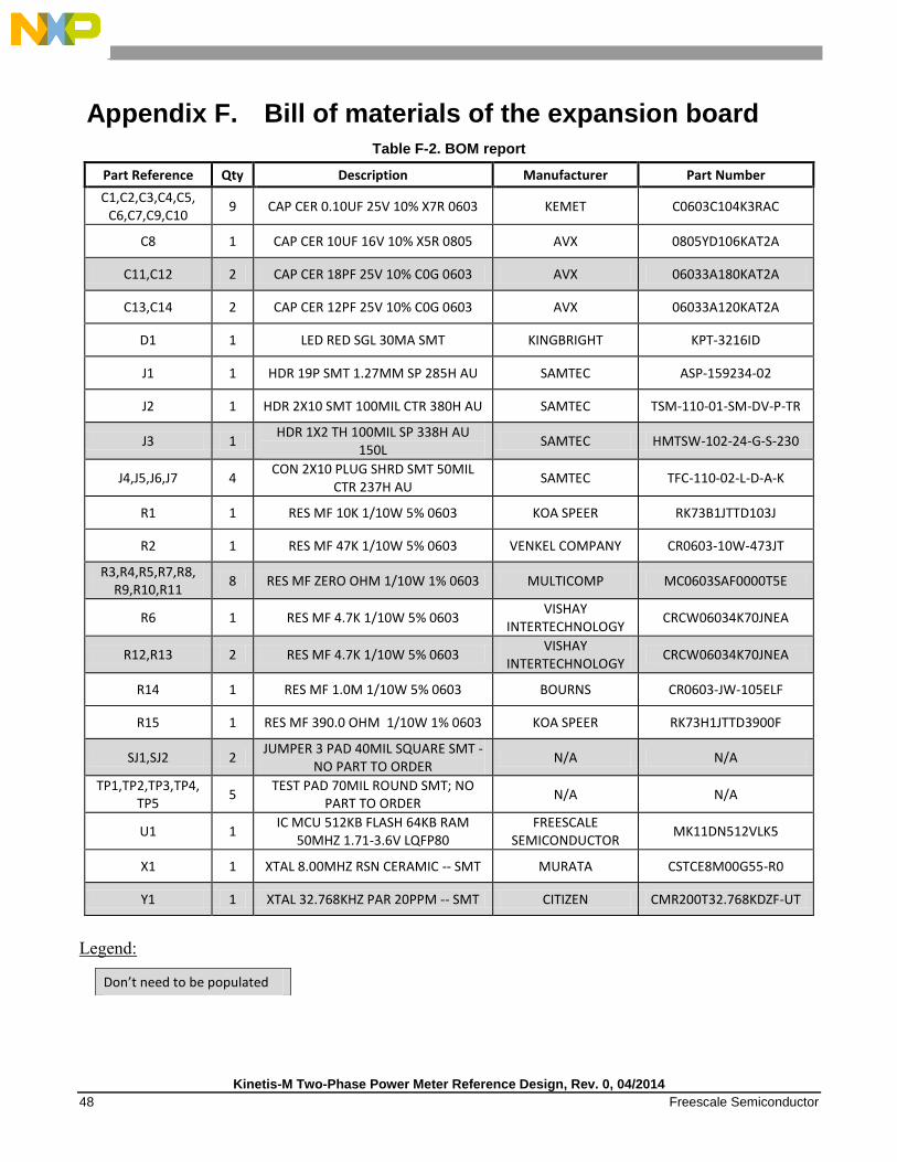
Kinetis-M Two-Phase Power Meter Reference Design, Rev. 0, 04/2014
48 Freescale Semiconductor
Appendix F. Bill of materials of the expansion board
Table F-2. BOM report
Part Reference Qty Description Manufacturer Part Number
C1,C2,C3,C4,C5, C6,C7,C9,C10
9 CAP CER 0.10UF 25V 10% X7R 0603 KEMET C0603C104K3RAC
C8 1 CAP CER 10UF 16V 10% X5R 0805 AVX 0805YD106KAT2A
C11,C12 2 CAP CER 18PF 25V 10% C0G 0603 AVX 06033A180KAT2A
C13,C14 2 CAP CER 12PF 25V 10% C0G 0603 AVX 06033A120KAT2A
D1 1 LED RED SGL 30MA SMT KINGBRIGHT KPT-3216ID
J1 1 HDR 19P SMT 1.27MM SP 285H AU SAMTEC ASP-159234-02
J2 1 HDR 2X10 SMT 100MIL CTR 380H AU SAMTEC TSM-110-01-SM-DV-P-TR
J3 1 HDR 1X2 TH 100MIL SP 338H AU
150L SAMTEC HMTSW-102-24-G-S-230
J4,J5,J6,J7 4 CON 2X10 PLUG SHRD SMT 50MIL
CTR 237H AU SAMTEC TFC-110-02-L-D-A-K
R1 1 RES MF 10K 1/10W 5% 0603 KOA SPEER RK73B1JTTD103J
R2 1 RES MF 47K 1/10W 5% 0603 VENKEL COMPANY CR0603-10W-473JT
R3,R4,R5,R7,R8, R9,R10,R11
8 RES MF ZERO OHM 1/10W 1% 0603 MULTICOMP MC0603SAF0000T5E
R6 1 RES MF 4.7K 1/10W 5% 0603 VISHAY
INTERTECHNOLOGY CRCW06034K70JNEA
R12,R13 2 RES MF 4.7K 1/10W 5% 0603 VISHAY
INTERTECHNOLOGY CRCW06034K70JNEA
R14 1 RES MF 1.0M 1/10W 5% 0603 BOURNS CR0603-JW-105ELF
R15 1 RES MF 390.0 OHM 1/10W 1% 0603 KOA SPEER RK73H1JTTD3900F
SJ1,SJ2 2 JUMPER 3 PAD 40MIL SQUARE SMT -
NO PART TO ORDER N/A N/A
TP1,TP2,TP3,TP4, TP5
5 TEST PAD 70MIL ROUND SMT; NO
PART TO ORDER N/A N/A
U1 1 IC MCU 512KB FLASH 64KB RAM
50MHZ 1.71-3.6V LQFP80 FREESCALE
SEMICONDUCTOR MK11DN512VLK5
X1 1 XTAL 8.00MHZ RSN CERAMIC -- SMT MURATA CSTCE8M00G55-R0
Y1 1 XTAL 32.768KHZ PAR 20PPM -- SMT CITIZEN CMR200T32.768KDZF-UT
Legend:
Don’t need to be populated

Document Number: DRM149
Rev. 0
04/2014
How to Reach Us:
Home Page:
freescale.com
Web Support:
freescale.com/support
Information in this document is provided solely to enable system and software implementers to use Freescale products. There are no express or implied copyright licenses granted hereunder to design or fabricate any integrated circuits based on the information in this document.
Freescale reserves the right to make changes without further notice to any products herein. Freescale makes no warranty, representation, or guarantee regarding the suitability of its products for any particular purpose, nor does Freescale assume any liability arising out of the application or use of any product or circuit, and specifically disclaims any and all liability, including without limitation consequential or incidental damages. “Typical” parameters that may be provided in Freescale data sheets and/or specifications can and do vary in different applications, and actual performance may vary over time. All operating parameters, including “typicals,” must be validated for each customer application by customer’s technical experts. Freescale does not convey any license under its patent rights nor the rights of others. Freescale sells products pursuant to standard terms and conditions of sale, which can be found at the following address: freescale.com/SalesTermsandConditions.
Freescale, the Freescale logo, and Kinetis, are trademarks of Freescale Semiconductor, Inc., Reg. U.S. Pat. & Tm. Off. All other product or service names are the property of their respective owners.
© Freescale Semiconductor, Inc. 2014. All rights reserved.