Embed Size (px)
Citation preview
For Academic Use Only
This material exempt per Department of Commerce license exception TSU
Lab 5 – SDK Lab
Targeting MicroBlaze™ on the Spartan-3E™
Starter Kit
SDK Lab: www.xilinx.com/university 5-3 MicroBlaze Processor [email protected]
Lab 5: SDK Lab
Introduction
This lab guides you through the process of adding timer and interrupt controller to an embedded system and writing a software application that utilizes these timer and interrupt controller. The SDK will be used to
create and debug the software application.
Objectives
After completing this lab, you will be able to:
• Utilize the XPS timer with interrupt controller
• Assign an interrupt handler to the timer
• Develop an interrupt handler function
• Use SDK Debugger to set break points and view the content of variables and memory
Procedure
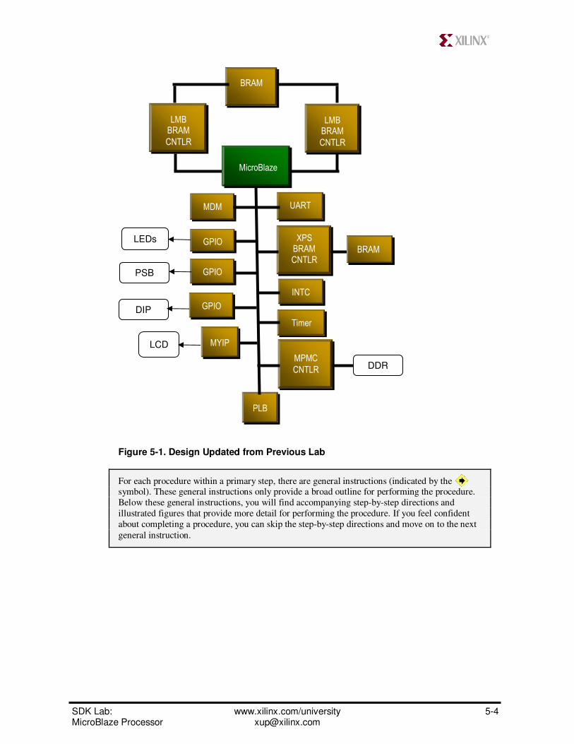
You will extend the hardware design created in lab 5 to include an XPS interrupt controller and XPS Timer
(see Figure 5-1). You will develop an interrupt handler to count the interrupts generated from the timer.
The steps for completing the lab are listed below:
1. Add a timer and interrupt controller
2. Create a SDK software project
3. Write an Interrupt Handler
4. Add a Linker script
5. Verify operation in hardware
SDK Lab: www.xilinx.com/university 5-4 MicroBlaze Processor [email protected]
Figure 5-1. Design Updated from Previous Lab
For each procedure within a primary step, there are general instructions (indicated by the symbol). These general instructions only provide a broad outline for performing the procedure.
Below these general instructions, you will find accompanying step-by-step directions and
illustrated figures that provide more detail for performing the procedure. If you feel confident
about completing a procedure, you can skip the step-by-step directions and move on to the next
general instruction.
LMB
BRAM
CNTLR
LMB
BRAM
CNTLR
BRAM
PLB
MDM UART
INTC
MicroBlaze
Timer
GPIO
GPIO
PSB
LEDs
LCD MYIP
GPIO DIP
BRAM
XPS
BRAM
CNTLR
MPMC
CNTLR DDR
SDK Lab: www.xilinx.com/university 5-5 MicroBlaze Processor [email protected]
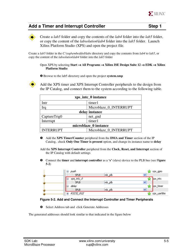
Add a Timer and Interrupt Controller Step 1
Create a lab5 folder and copy the contents of the lab4 folder into the lab5 folder,
or copy the content of the labsolution\lab4 folder into the lab5 folder. Launch
Xilinx Platform Studio (XPS) and open the project file.
Create a lab5 folder in the C:\xup\embedded\labs directory and copy the contents from lab4 to lab5, or
copy the content of the labsolution\lab4 folder into the lab5 folder
Open XPS by selecting Start →→→→ All Programs →→→→ Xilinx ISE Design Suite 12 →→→→ EDK →→→→ Xilinx
Platform Studio
� Browse to the lab5 directory and open the project system.xmp
Add the XPS timer and XPS Interrupt Controller peripherals to the design from
the IP Catalog, and connect them to the system according to the following table.
xps_intc_0 instance
Intr timer1
Irq Microblaze_0_INTERRUPT
delay instance
CaptureTrig0 net_gnd
Interrupt timer1
microblaze_0 instance
INTERRUPT Microblaze_0_INTERRUPT
� Add the XPS Timer/Counter peripheral from the DMA and Timer section of the IP
Catalog, check Only One Timer is present option, and change its instance name to delay
Add the XPS Interrupt Controller peripheral from the Clock, Reset, and Interrupt section of
the IP Catalog with default settings
� Connect the timer and interrupt controller as a ‘s’ (slave) device to the PLB bus (see Figure
5-2)
Figure 5-2. Add and Connect the Interrupt Controller and Timer Peripherals
� Select Address tab and click Generate Addresses
The generated addresses should look similar to that indicated in the figure below
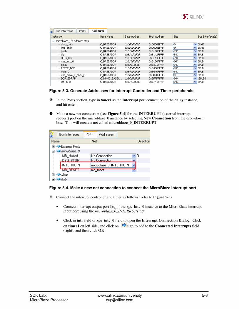
SDK Lab: www.xilinx.com/university 5-6 MicroBlaze Processor [email protected]
Figure 5-3. Generate Addresses for Interrupt Controller and Timer peripherals
� In the Ports section, type in timer1 as the Interrupt port connection of the delay instance,
and hit enter
� Make a new net connection (see Figure 5-4) for the INTERRUPT (external interrupt
request) port on the microblaze_0 instance by selecting New Connection from the drop-down box. This will create a net called microblaze_0_INTERRUPT
Figure 5-4. Make a new net connection to connect the MicroBlaze Interrupt port
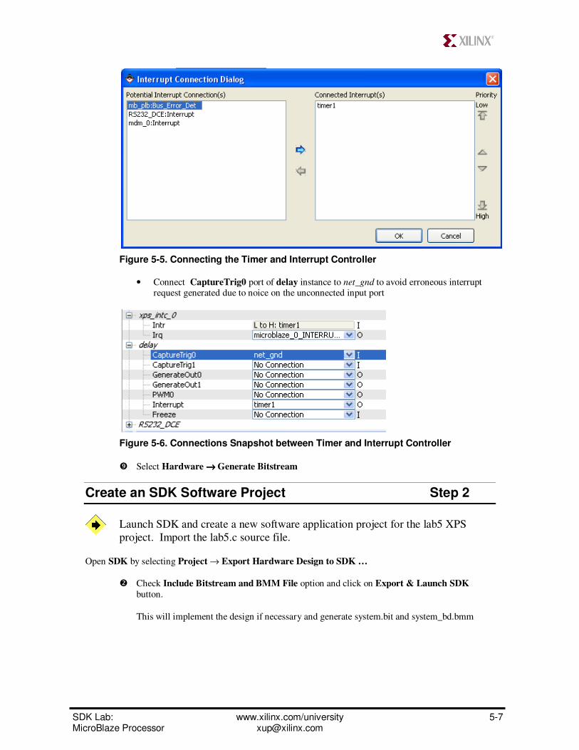
� Connect the interrupt controller and timer as follows (refer to Figure 5-5)
• Connect interrupt output port Irq of the xps_intc_0 instance to the MicroBlaze interrupt
input port using the microblaze_0_INTERRUPT net
• Click in intr field of xps_intc_0 field to open the Interrupt Connection Dialog. Click
on timer1 on left side, and click on sign to add to the Connected Interrupts field (right), and then click OK
SDK Lab: www.xilinx.com/university 5-7 MicroBlaze Processor [email protected]
Figure 5-5. Connecting the Timer and Interrupt Controller
• Connect CaptureTrig0 port of delay instance to net_gnd to avoid erroneous interrupt request generated due to noice on the unconnected input port
Figure 5-6. Connections Snapshot between Timer and Interrupt Controller
� Select Hardware →→→→ Generate Bitstream
Create an SDK Software Project Step 2
Launch SDK and create a new software application project for the lab5 XPS
project. Import the lab5.c source file.
Open SDK by selecting Project → Export Hardware Design to SDK …
� Check Include Bitstream and BMM File option and click on Export & Launch SDK
button.
This will implement the design if necessary and generate system.bit and system_bd.bmm

SDK Lab: www.xilinx.com/university 5-8 MicroBlaze Processor [email protected]
Figure 5-7. Export to SDK and Launch SDK
� Right-click on standalone_bsp_0 in the Project Explorer window and select New C Project
� Enter lab5 in the Project Name field and choose Empty Project in Project type window
Click Finish
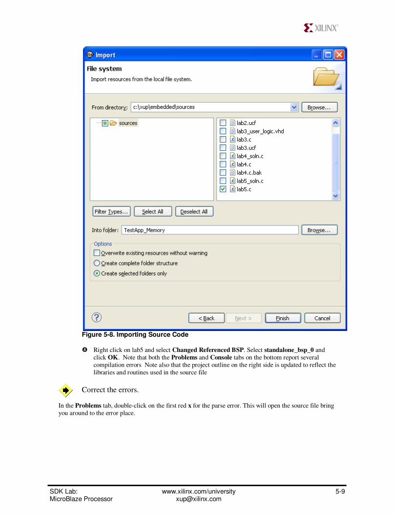
� Select lab5 in the project view, right-click, and select Import
� Extend the General folder and Double-click on File System and browse to
c:\xup\embedded\sources. Select lab5.c and click Finish
SDK Lab: www.xilinx.com/university 5-9 MicroBlaze Processor [email protected]
Figure 5-8. Importing Source Code
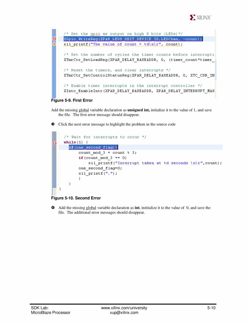
� Right click on lab5 and select Changed Referenced BSP. Select standalone_bsp_0 and
click OK. Note that both the Problems and Console tabs on the bottom report several
compilation errors Note also that the project outline on the right side is updated to reflect the
libraries and routines used in the source file
Correct the errors.
In the Problems tab, double-click on the first red x for the parse error. This will open the source file bring
you around to the error place.
SDK Lab: www.xilinx.com/university 5-10 MicroBlaze Processor [email protected]
Figure 5-9. First Error
Add the missing global variable declaration as unsigned int, initialize it to the value of 1, and save
the file. The first error message should disappear.
� Click the next error message to highlight the problem in the source code
Figure 5-10. Second Error
� Add the missing global variable declaration as int, inititalize it to the value of 0, and save the
file. The additional error messages should disappear.
SDK Lab: www.xilinx.com/university 5-11 MicroBlaze Processor [email protected]
Write an Interrupt Handler Step 3
Create the interrupt handler for the XPS timer
Go to where the interrupt handler function has already been stubbed out in the source file (a fast way to do
this is to click on the function in the outline view).
Create new local variable for the timer_int_handler function:
unsigned int csr;
The first step in creating an XPS timer interrupt handler is to verify that the XPS
timer caused the interrupt. This can be determined by looking at the XPS Timer
Control Status Register. Open the API documentation to determine how the
Control Status Register works.
In the XPS System Assembly View window, right-click the delay instance and select View PDF
Datasheet to open the data sheet
Go to the Register Description section in the data sheet and study the TCSR0 Register. Notice
that bit 23 has the following description:
Timer0 Interrupt Indicates that the condition for an interrupt on this timer has occurred. If the timer mode is
capture and the timer is enabled, this bit indicates a capture has occurred. If the mode is
generate, this bit indicates the counter has rolled over. Must be cleared by writing a 1
Read:
0 - No interrupt has occurred
1 - Interrupt has occurred
Write:
0 No change in state of T0INT
1 Clear T0INT (clear to ’0’)
The level 0 driver for the XPS timer provides two functions that read and write to the Control
Status Register. View the timer API doc by right-clicking on the delay instance in the System
Assembly View and selecting Driver:tmrctr_v2_00_a � View API Documentation. In the
API document, click on the File List link at the top of the document, then click on the link
labeled xtmrctr_l.h in the file list. This brings up the document on identifiers and the low-
level driver functions declared in this header file. Scroll down in the document and click on
the link for the XTmrCtr_GetControlStatusReg( ) function to read more about this
function. Use this function to determine whether an interrupt has occurred. The following is
the pertinent information found in the XPS timer documentation:
XTmrCtr_GetControlStatusReg ( BaseAddress, TmrCtrNumber )
Get the Control Status Register of a timer counter
Parameters:

SDK Lab: www.xilinx.com/university 5-12 MicroBlaze Processor [email protected]
o BaseAddress is the base address of the device. o TmrCtrNumber is the specific timer counter within the device, a zero-based
number, 0 -> (XTC_DEVICE_TIMER_COUNT - 1)
Returns:
o The value read from the register, a 32-bit value
� Add the XTmrCtr_GetControlStatusReg function call to the code with the associated parameters. The resulting 32-bit return value should be stored in the variable csr.
csr = XTmrCtr_GetControlStatusReg(baseaddr, 0);
Note: Substitute baseaddr with the base address for the delay peripheral. Refer to
xparameters.h
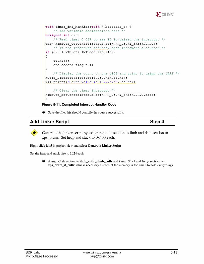
� Complete the Interrupt handler (see Figure 5-15) according to the steps below
1. Test to see if bit 23 is set by ANDing csr with the XTC_CSR_INT_OCCURED_MASK
parameter.
2. Increment a counter if an interrupt was taken.
3. Display the count value by using the LEDs_8Bit peripheral and print the value using
xil_printf (same functionality as printf with the exception of floating-point handling)
Hint: You may use the XGpio_DiscreteWrite () function
4. Clear the interrupt by using the following function call:
XTmrCtr_SetControlStatusReg(baseaddr, 0, csr);
The completed handler should look like as shown in the next figure
SDK Lab: www.xilinx.com/university 5-13 MicroBlaze Processor [email protected]
Figure 5-11. Completed Interrupt Handler Code
Save the file, this should compile the source successully.
Add Linker Script Step 4
Generate the linker script by assigning code section to ilmb and data section to
xps_bram. Set heap and stack to 0x400 each.
Right-click lab5 in project view and select Generate Linker Script
Set the heap and stack size to 1024 each
� Assign Code section to ilmb_cntlr_dlmb_cntlr and Data, Stack and Heap sections to
xps_bram_if_cntlr (this is necessary as each of the memory is too small to hold everything)

SDK Lab: www.xilinx.com/university 5-14 MicroBlaze Processor [email protected]
Figure 5-12. Generate Linker Script
� Click Generate to generate the linker script, add to the project and recompile the program.
Look in the console to answer the following question.
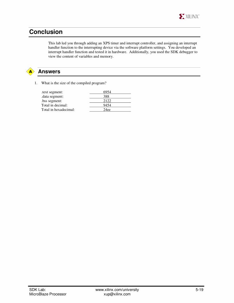
1. What is the size of the compiled program?
.text segment:
.data segment:
.bss segment:
Total in decimal:
Total in hexadecimal:
Verify Operation in Hardware Step 5
Generate the bitstream and download to the Spartan-3E starter kit.
Connect and power the board
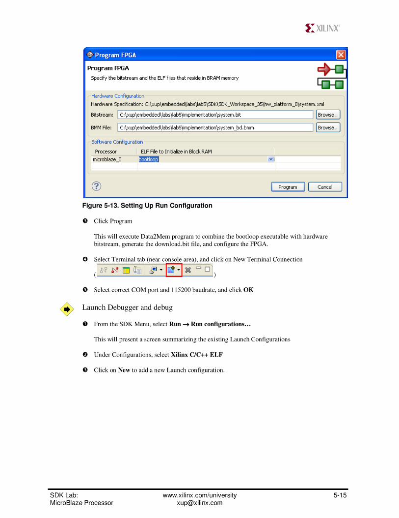
� Select Xilinx Tools ���� Program FPGA
� Browse and select system.bit and system_bd.bmm files from the lab5\implementation (this
step is required for 12.2 version. For other version, you may skip this step and try with the
default paths to see if it works)
?
SDK Lab: www.xilinx.com/university 5-15 MicroBlaze Processor [email protected]
Figure 5-13. Setting Up Run Configuration
� Click Program
This will execute Data2Mem program to combine the bootloop executable with hardware
bitstream, generate the download.bit file, and configure the FPGA.
� Select Terminal tab (near console area), and click on New Terminal Connection
( )
Select correct COM port and 115200 baudrate, and click OK
Launch Debugger and debug
� From the SDK Menu, select Run →→→→ Run configurations…
This will present a screen summarizing the existing Launch Configurations
� Under Configurations, select Xilinx C/C++ ELF
� Click on New to add a new Launch configuration.
SDK Lab: www.xilinx.com/university 5-16 MicroBlaze Processor [email protected]
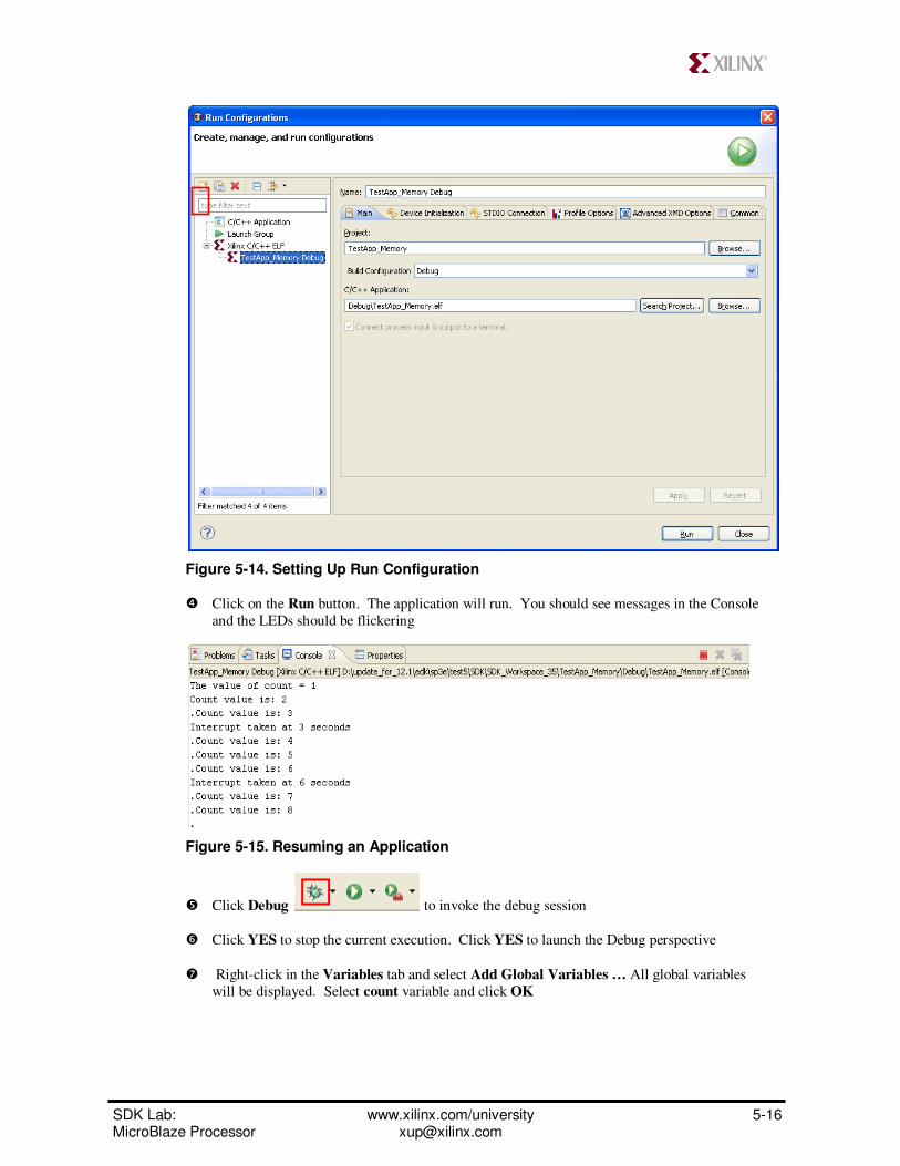
Figure 5-14. Setting Up Run Configuration
� Click on the Run button. The application will run. You should see messages in the Console
and the LEDs should be flickering
Figure 5-15. Resuming an Application
Click Debug to invoke the debug session
� Click YES to stop the current execution. Click YES to launch the Debug perspective
� Right-click in the Variables tab and select Add Global Variables … All global variables
will be displayed. Select count variable and click OK

SDK Lab: www.xilinx.com/university 5-17 MicroBlaze Processor [email protected]
Monitor variables and memory content.
� Double-click to set a breakpoint on the line in lab5.c where count is written to LED
Figure 5-16. Setting Breakpoint
� Click on Resume button to continue executing the program up until the breakpoint.
As you do step over, you will notice that the count variable value is changing.
� Click on the memory tab. If you do not see it, go to Window ���� Show View ���� Memory
� Click the sign to add a Memory Monitor
Figure 5-17. Adding Memory Address
Enter the address for the count variable as follows, and click OK

SDK Lab: www.xilinx.com/university 5-18 MicroBlaze Processor [email protected]
Figure 5-18. Monitoring a Variable
� Click the Resume button to continue execution of the program.
Notice that the count variables increment every time you click resume.
Figure 5-19. Viewing Memory Content of the count variable
� Terminate the session by clicking on the Terminate button.
Figure 5-20. Terminating a Debug Session
� Close the SDK application and close the XPS project
Click to terminate
session
Watch count
value increment
SDK Lab: www.xilinx.com/university 5-19 MicroBlaze Processor [email protected]
Conclusion
This lab led you through adding an XPS timer and interrupt controller, and assigning an interrupt handler function to the interrupting device via the software platform settings. You developed an
interrupt handler function and tested it in hardware. Additionally, you used the SDK debugger to
view the content of variables and memory.
Answers
1. What is the size of the compiled program?
.text segment: 6954
.data segment: 388
.bss segment: 2122
Total in decimal: 9454
Total in hexadecimal: 24ee
A
SDK Lab: www.xilinx.com/university 5-20 MicroBlaze Processor [email protected]
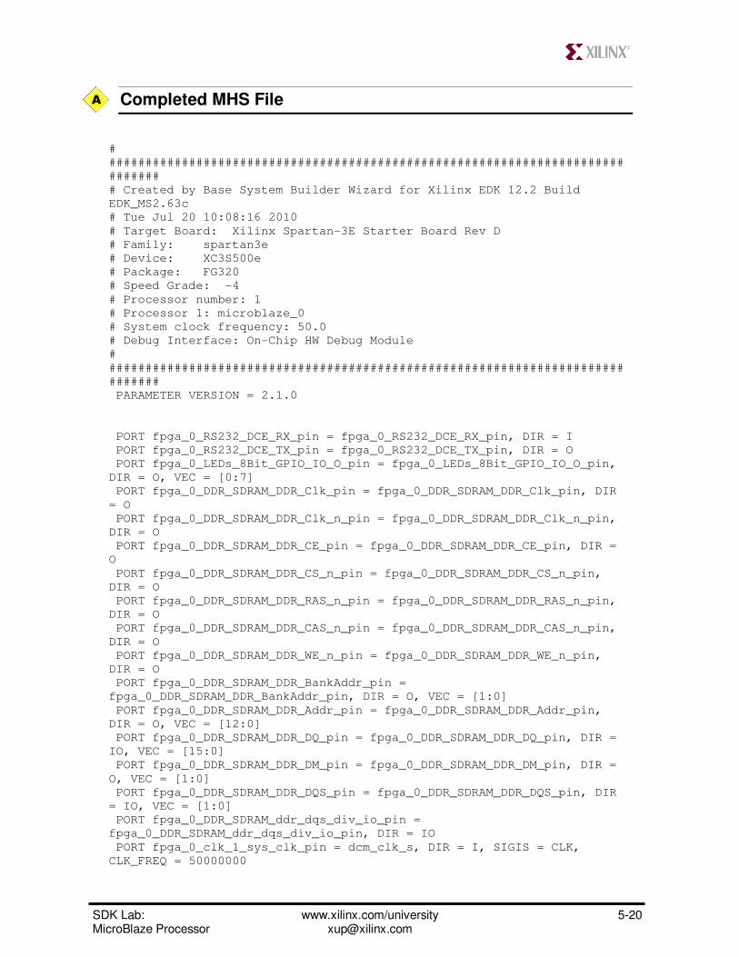
Completed MHS File
#
#######################################################################
#######
# Created by Base System Builder Wizard for Xilinx EDK 12.2 Build
EDK_MS2.63c
# Tue Jul 20 10:08:16 2010
# Target Board: Xilinx Spartan-3E Starter Board Rev D
# Family: spartan3e
# Device: XC3S500e
# Package: FG320
# Speed Grade: -4
# Processor number: 1
# Processor 1: microblaze_0
# System clock frequency: 50.0
# Debug Interface: On-Chip HW Debug Module
#
#######################################################################
#######
PARAMETER VERSION = 2.1.0
PORT fpga_0_RS232_DCE_RX_pin = fpga_0_RS232_DCE_RX_pin, DIR = I
PORT fpga_0_RS232_DCE_TX_pin = fpga_0_RS232_DCE_TX_pin, DIR = O
PORT fpga_0_LEDs_8Bit_GPIO_IO_O_pin = fpga_0_LEDs_8Bit_GPIO_IO_O_pin,
DIR = O, VEC = [0:7]
PORT fpga_0_DDR_SDRAM_DDR_Clk_pin = fpga_0_DDR_SDRAM_DDR_Clk_pin, DIR
= O
PORT fpga_0_DDR_SDRAM_DDR_Clk_n_pin = fpga_0_DDR_SDRAM_DDR_Clk_n_pin,
DIR = O
PORT fpga_0_DDR_SDRAM_DDR_CE_pin = fpga_0_DDR_SDRAM_DDR_CE_pin, DIR =
O
PORT fpga_0_DDR_SDRAM_DDR_CS_n_pin = fpga_0_DDR_SDRAM_DDR_CS_n_pin,
DIR = O
PORT fpga_0_DDR_SDRAM_DDR_RAS_n_pin = fpga_0_DDR_SDRAM_DDR_RAS_n_pin,
DIR = O
PORT fpga_0_DDR_SDRAM_DDR_CAS_n_pin = fpga_0_DDR_SDRAM_DDR_CAS_n_pin,
DIR = O
PORT fpga_0_DDR_SDRAM_DDR_WE_n_pin = fpga_0_DDR_SDRAM_DDR_WE_n_pin,
DIR = O
PORT fpga_0_DDR_SDRAM_DDR_BankAddr_pin =
fpga_0_DDR_SDRAM_DDR_BankAddr_pin, DIR = O, VEC = [1:0]
PORT fpga_0_DDR_SDRAM_DDR_Addr_pin = fpga_0_DDR_SDRAM_DDR_Addr_pin,
DIR = O, VEC = [12:0]
PORT fpga_0_DDR_SDRAM_DDR_DQ_pin = fpga_0_DDR_SDRAM_DDR_DQ_pin, DIR =
IO, VEC = [15:0]
PORT fpga_0_DDR_SDRAM_DDR_DM_pin = fpga_0_DDR_SDRAM_DDR_DM_pin, DIR =
O, VEC = [1:0]
PORT fpga_0_DDR_SDRAM_DDR_DQS_pin = fpga_0_DDR_SDRAM_DDR_DQS_pin, DIR
= IO, VEC = [1:0]
PORT fpga_0_DDR_SDRAM_ddr_dqs_div_io_pin =
fpga_0_DDR_SDRAM_ddr_dqs_div_io_pin, DIR = IO
PORT fpga_0_clk_1_sys_clk_pin = dcm_clk_s, DIR = I, SIGIS = CLK,
CLK_FREQ = 50000000
A

SDK Lab: www.xilinx.com/university 5-21 MicroBlaze Processor [email protected]
PORT fpga_0_rst_1_sys_rst_pin = sys_rst_s, DIR = I, SIGIS = RST,
RST_POLARITY = 1
PORT push_GPIO_IO_I_pin = push_GPIO_IO_I, DIR = I, VEC = [0:3]
PORT dip_GPIO_IO_I_pin = dip_GPIO_IO_I, DIR = I, VEC = [0:3]
PORT lcd_ip_0_lcd_pin = lcd_ip_0_lcd, DIR = O, VEC = [0:6]
BEGIN microblaze
PARAMETER INSTANCE = microblaze_0
PARAMETER C_AREA_OPTIMIZED = 1
PARAMETER C_DEBUG_ENABLED = 1
PARAMETER HW_VER = 7.30.b
BUS_INTERFACE DLMB = dlmb
BUS_INTERFACE ILMB = ilmb
BUS_INTERFACE DPLB = mb_plb
BUS_INTERFACE IPLB = mb_plb
BUS_INTERFACE DEBUG = microblaze_0_mdm_bus
PORT MB_RESET = mb_reset
PORT INTERRUPT = microblaze_0_INTERRUPT
END
BEGIN plb_v46
PARAMETER INSTANCE = mb_plb
PARAMETER HW_VER = 1.04.a
PORT PLB_Clk = clk_50_0000MHz
PORT SYS_Rst = sys_bus_reset
END
BEGIN lmb_v10
PARAMETER INSTANCE = ilmb
PARAMETER HW_VER = 1.00.a
PORT LMB_Clk = clk_50_0000MHz
PORT SYS_Rst = sys_bus_reset
END
BEGIN lmb_v10
PARAMETER INSTANCE = dlmb
PARAMETER HW_VER = 1.00.a
PORT LMB_Clk = clk_50_0000MHz
PORT SYS_Rst = sys_bus_reset
END
BEGIN lmb_bram_if_cntlr
PARAMETER INSTANCE = dlmb_cntlr
PARAMETER HW_VER = 2.10.b
PARAMETER C_BASEADDR = 0x00000000
PARAMETER C_HIGHADDR = 0x00001fff
BUS_INTERFACE SLMB = dlmb
BUS_INTERFACE BRAM_PORT = dlmb_port
END
BEGIN lmb_bram_if_cntlr
PARAMETER INSTANCE = ilmb_cntlr
PARAMETER HW_VER = 2.10.b
PARAMETER C_BASEADDR = 0x00000000
PARAMETER C_HIGHADDR = 0x00001fff
BUS_INTERFACE SLMB = ilmb
SDK Lab: www.xilinx.com/university 5-22 MicroBlaze Processor [email protected]
BUS_INTERFACE BRAM_PORT = ilmb_port
END
BEGIN bram_block
PARAMETER INSTANCE = lmb_bram
PARAMETER HW_VER = 1.00.a
BUS_INTERFACE PORTA = ilmb_port
BUS_INTERFACE PORTB = dlmb_port
END
BEGIN xps_uartlite
PARAMETER INSTANCE = RS232_DCE
PARAMETER C_BAUDRATE = 115200
PARAMETER C_DATA_BITS = 8
PARAMETER C_USE_PARITY = 0
PARAMETER C_ODD_PARITY = 0
PARAMETER HW_VER = 1.01.a
PARAMETER C_BASEADDR = 0x84000000
PARAMETER C_HIGHADDR = 0x8400ffff
BUS_INTERFACE SPLB = mb_plb
PORT RX = fpga_0_RS232_DCE_RX_pin
PORT TX = fpga_0_RS232_DCE_TX_pin
END
BEGIN xps_gpio
PARAMETER INSTANCE = LEDs_8Bit
PARAMETER C_ALL_INPUTS = 0
PARAMETER C_GPIO_WIDTH = 8
PARAMETER C_INTERRUPT_PRESENT = 0
PARAMETER C_IS_DUAL = 0
PARAMETER HW_VER = 2.00.a
PARAMETER C_BASEADDR = 0x81440000
PARAMETER C_HIGHADDR = 0x8144ffff
BUS_INTERFACE SPLB = mb_plb
PORT GPIO_IO_O = fpga_0_LEDs_8Bit_GPIO_IO_O_pin
END
BEGIN mpmc
PARAMETER INSTANCE = DDR_SDRAM
PARAMETER C_NUM_PORTS = 1
PARAMETER C_SPECIAL_BOARD = S3E_STKIT
PARAMETER C_MEM_TYPE = DDR
PARAMETER C_MEM_PARTNO = MT46V32M16-6
PARAMETER C_MEM_DATA_WIDTH = 16
PARAMETER C_PIM0_BASETYPE = 2
PARAMETER HW_VER = 6.01.a
PARAMETER C_MPMC_BASEADDR = 0x8c000000
PARAMETER C_MPMC_HIGHADDR = 0x8fffffff
BUS_INTERFACE SPLB0 = mb_plb
PORT MPMC_Clk0 = clk_100_0000MHzDCM0
PORT MPMC_Clk90 = clk_100_0000MHz90DCM0
PORT MPMC_Rst = sys_periph_reset
PORT DDR_Clk = fpga_0_DDR_SDRAM_DDR_Clk_pin
PORT DDR_Clk_n = fpga_0_DDR_SDRAM_DDR_Clk_n_pin
PORT DDR_CE = fpga_0_DDR_SDRAM_DDR_CE_pin
PORT DDR_CS_n = fpga_0_DDR_SDRAM_DDR_CS_n_pin
PORT DDR_RAS_n = fpga_0_DDR_SDRAM_DDR_RAS_n_pin

SDK Lab: www.xilinx.com/university 5-23 MicroBlaze Processor [email protected]
PORT DDR_CAS_n = fpga_0_DDR_SDRAM_DDR_CAS_n_pin
PORT DDR_WE_n = fpga_0_DDR_SDRAM_DDR_WE_n_pin
PORT DDR_BankAddr = fpga_0_DDR_SDRAM_DDR_BankAddr_pin
PORT DDR_Addr = fpga_0_DDR_SDRAM_DDR_Addr_pin
PORT DDR_DQ = fpga_0_DDR_SDRAM_DDR_DQ_pin
PORT DDR_DM = fpga_0_DDR_SDRAM_DDR_DM_pin
PORT DDR_DQS = fpga_0_DDR_SDRAM_DDR_DQS_pin
PORT DDR_DQS_Div_O = fpga_0_DDR_SDRAM_ddr_dqs_div_io_pin
PORT DDR_DQS_Div_I = fpga_0_DDR_SDRAM_ddr_dqs_div_io_pin
END
BEGIN clock_generator
PARAMETER INSTANCE = clock_generator_0
PARAMETER C_CLKIN_FREQ = 50000000
PARAMETER C_CLKOUT0_FREQ = 100000000
PARAMETER C_CLKOUT0_PHASE = 90
PARAMETER C_CLKOUT0_GROUP = DCM0
PARAMETER C_CLKOUT0_BUF = TRUE
PARAMETER C_CLKOUT1_FREQ = 100000000
PARAMETER C_CLKOUT1_PHASE = 0
PARAMETER C_CLKOUT1_GROUP = DCM0
PARAMETER C_CLKOUT1_BUF = TRUE
PARAMETER C_CLKOUT2_FREQ = 50000000
PARAMETER C_CLKOUT2_PHASE = 0
PARAMETER C_CLKOUT2_GROUP = NONE
PARAMETER C_CLKOUT2_BUF = TRUE
PARAMETER C_EXT_RESET_HIGH = 1
PARAMETER HW_VER = 4.00.a
PORT CLKIN = dcm_clk_s
PORT CLKOUT0 = clk_100_0000MHz90DCM0
PORT CLKOUT1 = clk_100_0000MHzDCM0
PORT CLKOUT2 = clk_50_0000MHz
PORT RST = sys_rst_s
PORT LOCKED = Dcm_all_locked
END
BEGIN mdm
PARAMETER INSTANCE = mdm_0
PARAMETER C_MB_DBG_PORTS = 1
PARAMETER C_USE_UART = 1
PARAMETER C_UART_WIDTH = 8
PARAMETER HW_VER = 1.00.g
PARAMETER C_BASEADDR = 0x84400000
PARAMETER C_HIGHADDR = 0x8440ffff
BUS_INTERFACE SPLB = mb_plb
BUS_INTERFACE MBDEBUG_0 = microblaze_0_mdm_bus
PORT Debug_SYS_Rst = Debug_SYS_Rst
END
BEGIN proc_sys_reset
PARAMETER INSTANCE = proc_sys_reset_0
PARAMETER C_EXT_RESET_HIGH = 1
PARAMETER HW_VER = 2.00.a
PORT Slowest_sync_clk = clk_50_0000MHz
PORT Ext_Reset_In = sys_rst_s
PORT MB_Debug_Sys_Rst = Debug_SYS_Rst
PORT Dcm_locked = Dcm_all_locked
SDK Lab: www.xilinx.com/university 5-24 MicroBlaze Processor [email protected]
PORT MB_Reset = mb_reset
PORT Bus_Struct_Reset = sys_bus_reset
PORT Peripheral_Reset = sys_periph_reset
END
BEGIN xps_gpio
PARAMETER INSTANCE = dip
PARAMETER HW_VER = 2.00.a
PARAMETER C_GPIO_WIDTH = 4
PARAMETER C_ALL_INPUTS = 1
PARAMETER C_BASEADDR = 0x81420000
PARAMETER C_HIGHADDR = 0x8142ffff
BUS_INTERFACE SPLB = mb_plb
PORT GPIO_IO_I = dip_GPIO_IO_I
END
BEGIN xps_gpio
PARAMETER INSTANCE = push
PARAMETER HW_VER = 2.00.a
PARAMETER C_GPIO_WIDTH = 4
PARAMETER C_ALL_INPUTS = 1
PARAMETER C_BASEADDR = 0x81400000
PARAMETER C_HIGHADDR = 0x8140ffff
BUS_INTERFACE SPLB = mb_plb
PORT GPIO_IO_I = push_GPIO_IO_I
END
BEGIN lcd_ip
PARAMETER INSTANCE = lcd_ip_0
PARAMETER HW_VER = 1.00.a
PARAMETER C_BASEADDR = 0xcf400000
PARAMETER C_HIGHADDR = 0xcf40ffff
BUS_INTERFACE SPLB = mb_plb
PORT lcd = lcd_ip_0_lcd
END
BEGIN bram_block
PARAMETER INSTANCE = bram_block_0
PARAMETER HW_VER = 1.00.a
BUS_INTERFACE PORTA = xps_bram_if_cntlr_0_PORTA
END
BEGIN xps_bram_if_cntlr
PARAMETER INSTANCE = xps_bram_if_cntlr_0
PARAMETER HW_VER = 1.00.b
PARAMETER C_SPLB_NATIVE_DWIDTH = 32
PARAMETER C_BASEADDR = 0x88208000
PARAMETER C_HIGHADDR = 0x88209fff
BUS_INTERFACE SPLB = mb_plb
BUS_INTERFACE PORTA = xps_bram_if_cntlr_0_PORTA
END
BEGIN xps_timer
PARAMETER INSTANCE = delay
PARAMETER HW_VER = 1.02.a
PARAMETER C_ONE_TIMER_ONLY = 1
PARAMETER C_BASEADDR = 0x83c00000

SDK Lab: www.xilinx.com/university 5-25 MicroBlaze Processor [email protected]
PARAMETER C_HIGHADDR = 0x83c0ffff
BUS_INTERFACE SPLB = mb_plb
PORT CaptureTrig0 = net_gnd
PORT Interrupt = timer1
END
BEGIN xps_intc
PARAMETER INSTANCE = xps_intc_0
PARAMETER HW_VER = 2.01.a
PARAMETER C_BASEADDR = 0x81800000
PARAMETER C_HIGHADDR = 0x8180ffff
BUS_INTERFACE SPLB = mb_plb
PORT Intr = timer1
PORT Irq = microblaze_0_INTERRUPT
END