Embed Size (px)
Citation preview
Lab 8: Op Amps III
Christopher AgostinoLab Partner: MacCallum Robertson
April 6, 2015
Introduction
In this lab we will be exploring a lot of the real world limitations on operational amplifiers. We will lookat the input offset voltages associated with op amp inputs as well as the biased input current associatedwith the inputs. We also will explore ways to minimize the input offset using a trimming potentiometer.We also will explore the finite output current of op amps as well as the existence of oscillations in opamp feedback loops. We will utilize Multisim to better understand how some of these circuits shouldwork theoretically and will gain an introduction to LabVIEW. We will also build a circuit which playsmusic and then improve the quality of it by using BJT’s and a push-pull stage inside of the op amp’sfeedback loop.
8.1
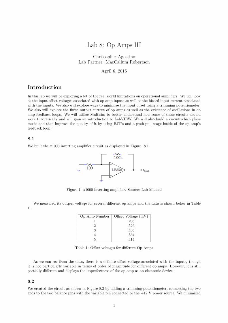
We built the x1000 inverting amplifier circuit as displayed in Figure 8.1.
Figure 1: x1000 inverting amplifier. Source: Lab Manual
We measured its output voltage for several different op amps and the data is shown below in Table1.
Op Amp Number Offset Voltage (mV)1 .2062 .5263 .4054 .5345 .414
Table 1: Offset voltages for different Op Amps
As we can see from the data, there is a definite offset voltage associated with the inputs, thoughit is not particularly variable in terms of order of magnitude for different op amps. However, it is stillpartially different and displays the imperfectness of the op amp as an electronic device.
8.2
We created the circuit as shown in Figure 8.2 by adding a trimming potentiometer, connecting the twoends to the two balance pins with the variable pin connected to the +12 V power source. We minimized
1
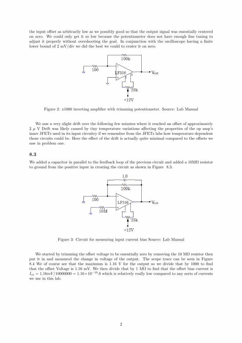
the input offset as arbitrarily low as we possibly good so that the output signal was essentially centeredon zero. We could only get it so low because the potentiometer does not have enough fine tuning toadjust it properly without overshooting the goal. In conjunction with the oscilloscope having a finitelower bound of 2 mV/div we did the best we could to center it on zero.
Figure 2: x1000 inverting amplifier with trimming potentiometer. Source: Lab Manual
We saw a very slight drift over the following few minutes where it reached an offset of approximately2 µ V Drift was likely caused by tiny temperature variations affecting the properties of the op amp’sinner JFETs used in its input circuitry if we remember from the JFETs labs how temperature dependentthose circuits could be. Here the effect of the drift is actually quite minimal compared to the offsets wesaw in problem one.
8.3
We added a capacitor in parallel to the feedback loop of the previous circuit and added a 10MΩ resistorto ground from the positive input in creating the circuit as shown in Figure 8.3.
Figure 3: Circuit for measuring input current bias Source: Lab Manual
We started by trimming the offset voltage to be essentially zero by removing the 10 MΩ resistor thenput it in and measured the change in voltage of the output. The scope trace can be seen in Figure8.4 We of course see that the maximum is 1.16 V for the output so we divide that by 1000 to findthat the offset Voltage is 1.16 mV. We then divide that by 1 MΩ to find that the offset bias current isIos = 1.16mV/10000000 = 1.16 ∗ 10−10A which is relatively really low compared to any sorts of currentswe use in this lab.
2
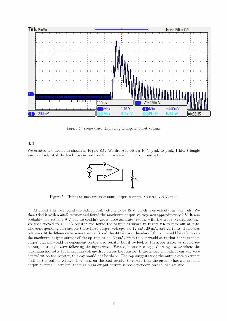
Figure 4: Scope trace displaying change in offset voltage
8.4
We created the circuit as shown in Figure 8.5. We drove it with a 10 V peak to peak, 1 kHz trianglewave and adjusted the load resistor until we found a maximum current output.
Figure 5: Circuit to measure maximum output current. Source: Lab Manual
At about 1 kΩ, we found the output peak voltage to be 12 V, which is essentially just the rails. Wethen tried it with a 306Ω resistor and found the maximum output voltage was approximately 9 V. It wasprobably not actually 9 V but we couldn’t get a more accurate reading with the scope on that setting.We then moved to a 99.8Ω resistor and found the output as shown in Figure 8.6 to max out at 2.92.The corresponding currents for those three output voltages are 12 mA, 29 mA, and 29.2 mA. There wasrelatively little difference between the 306 Ω and the 99.8Ω case, therefore I think it would be safe to capthe maximum output current of the op amp to be 30 mA. From this, it would seem that the maximumoutput current would be dependent on the load resistor but if we look at the scope trace, we should seean output triangle wave following the input wave. We see, however, a capped triangle wave where themaximum indicates the maximum voltage drop across the resistor. If the maximum output current weredependent on the resistor, this cap would not be there. The cap suggests that the output sets an upperlimit on the output voltage depending on the load resistor to ensure that the op amp has a maximumoutput current. Therefore, the maximum output current is not dependent on the load resistor.
3
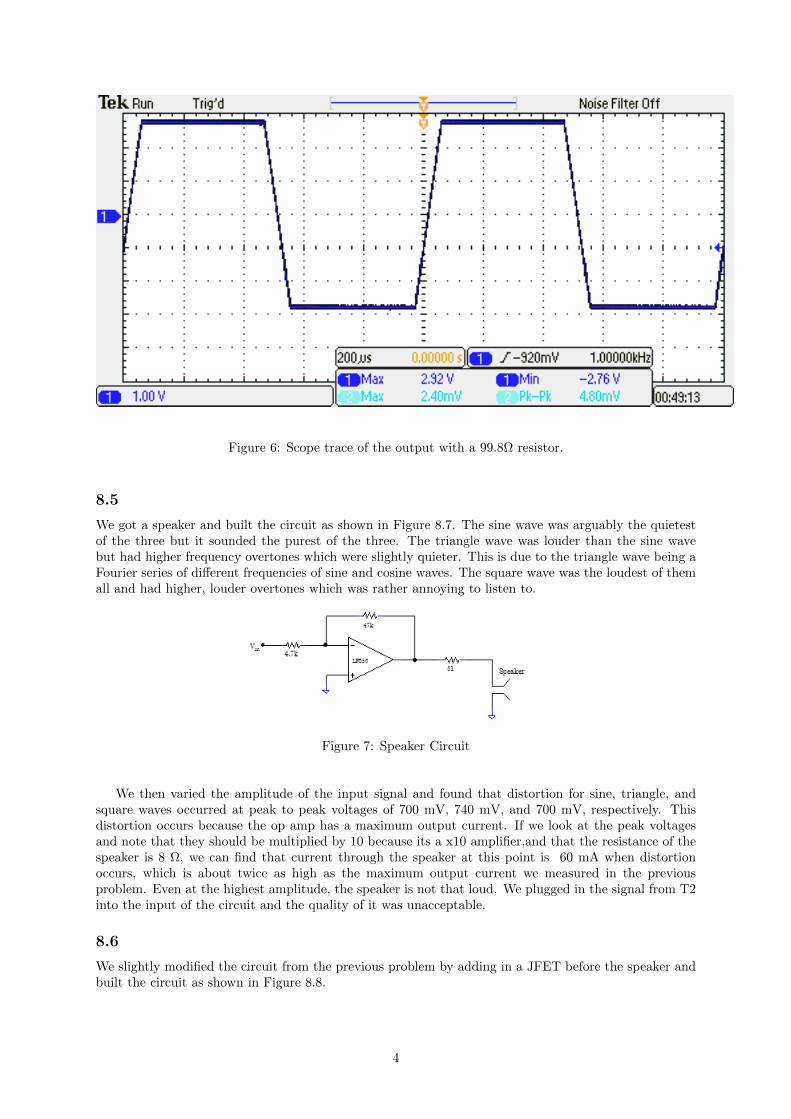
Figure 6: Scope trace of the output with a 99.8Ω resistor.
8.5
We got a speaker and built the circuit as shown in Figure 8.7. The sine wave was arguably the quietestof the three but it sounded the purest of the three. The triangle wave was louder than the sine wavebut had higher frequency overtones which were slightly quieter. This is due to the triangle wave being aFourier series of different frequencies of sine and cosine waves. The square wave was the loudest of themall and had higher, louder overtones which was rather annoying to listen to.
Figure 7: Speaker Circuit
We then varied the amplitude of the input signal and found that distortion for sine, triangle, andsquare waves occurred at peak to peak voltages of 700 mV, 740 mV, and 700 mV, respectively. Thisdistortion occurs because the op amp has a maximum output current. If we look at the peak voltagesand note that they should be multiplied by 10 because its a x10 amplifier,and that the resistance of thespeaker is 8 Ω, we can find that current through the speaker at this point is 60 mA when distortionoccurs, which is about twice as high as the maximum output current we measured in the previousproblem. Even at the highest amplitude, the speaker is not that loud. We plugged in the signal from T2into the input of the circuit and the quality of it was unacceptable.
8.6
We slightly modified the circuit from the previous problem by adding in a JFET before the speaker andbuilt the circuit as shown in Figure 8.8.
4
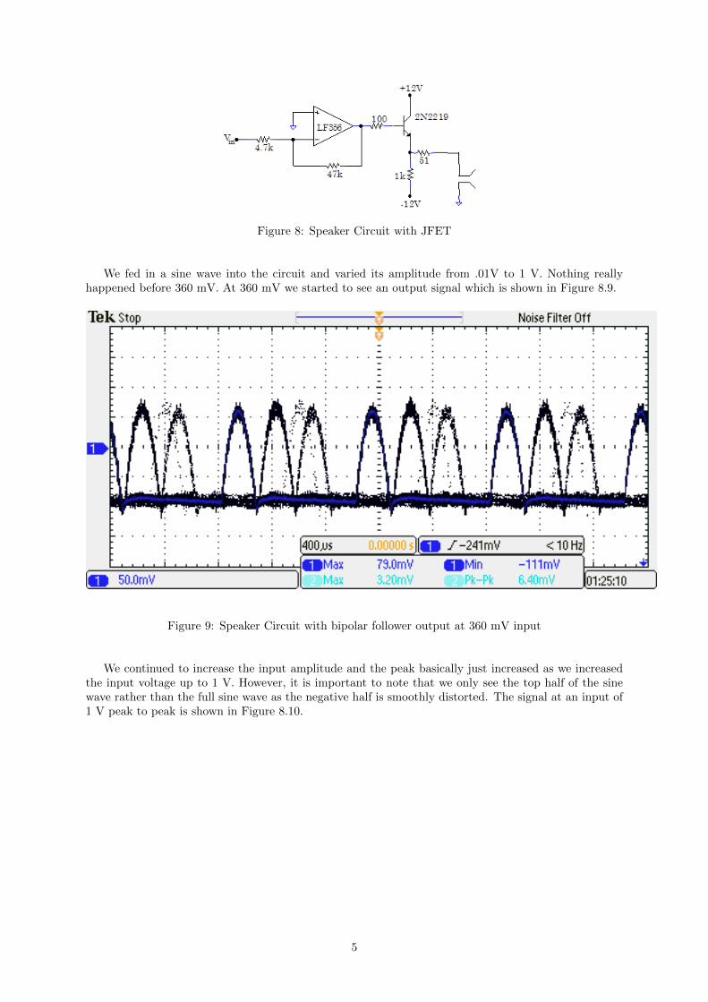
Figure 8: Speaker Circuit with JFET
We fed in a sine wave into the circuit and varied its amplitude from .01V to 1 V. Nothing reallyhappened before 360 mV. At 360 mV we started to see an output signal which is shown in Figure 8.9.
Figure 9: Speaker Circuit with bipolar follower output at 360 mV input
We continued to increase the input amplitude and the peak basically just increased as we increasedthe input voltage up to 1 V. However, it is important to note that we only see the top half of the sinewave rather than the full sine wave as the negative half is smoothly distorted. The signal at an input of1 V peak to peak is shown in Figure 8.10.
5
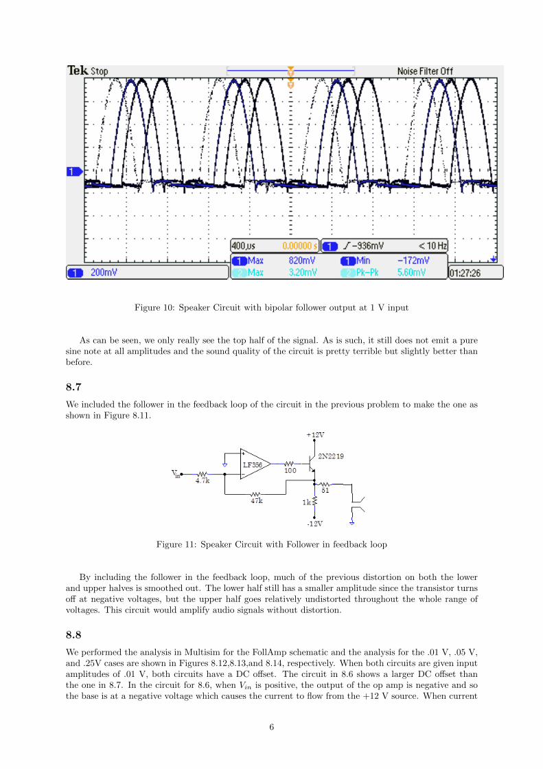
Figure 10: Speaker Circuit with bipolar follower output at 1 V input
As can be seen, we only really see the top half of the signal. As is such, it still does not emit a puresine note at all amplitudes and the sound quality of the circuit is pretty terrible but slightly better thanbefore.
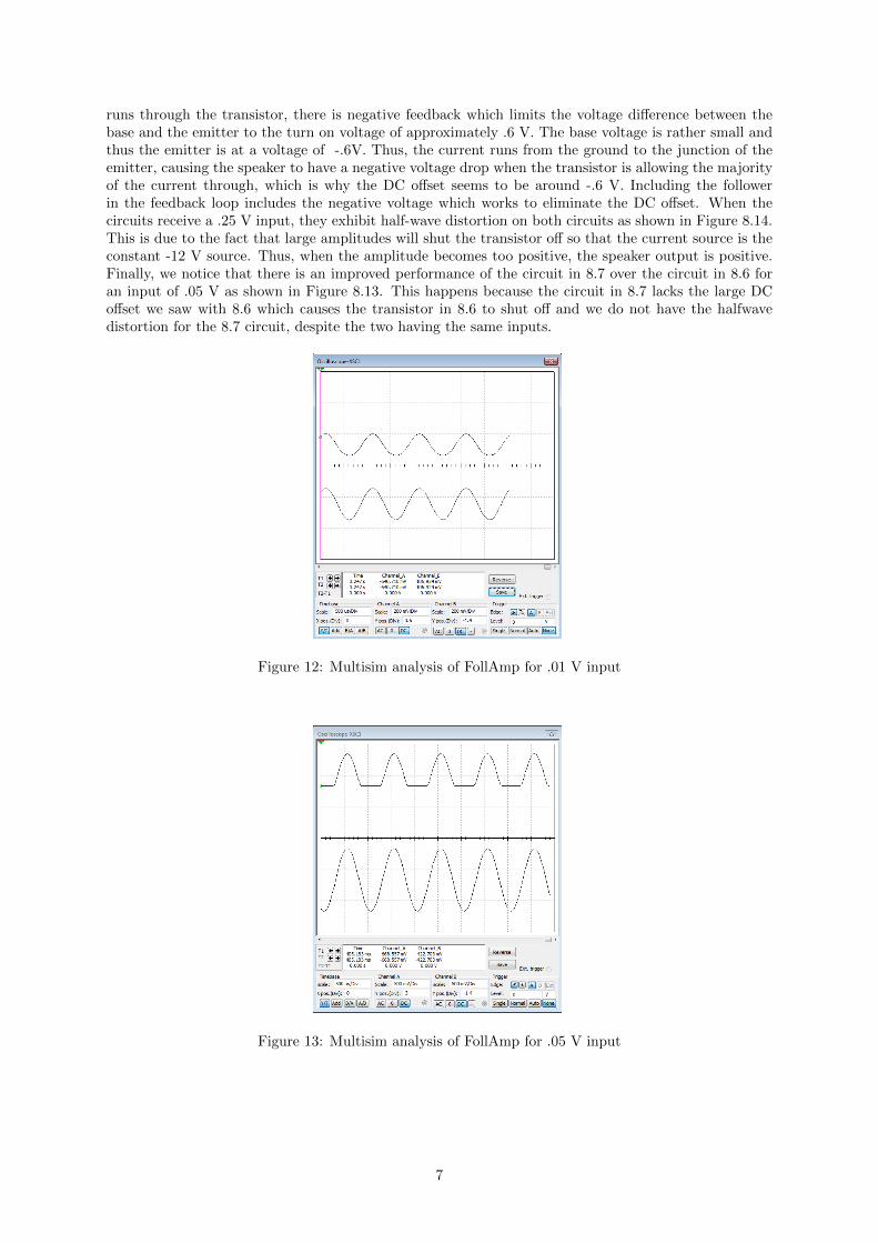
8.7
We included the follower in the feedback loop of the circuit in the previous problem to make the one asshown in Figure 8.11.
Figure 11: Speaker Circuit with Follower in feedback loop
By including the follower in the feedback loop, much of the previous distortion on both the lowerand upper halves is smoothed out. The lower half still has a smaller amplitude since the transistor turnsoff at negative voltages, but the upper half goes relatively undistorted throughout the whole range ofvoltages. This circuit would amplify audio signals without distortion.
8.8
We performed the analysis in Multisim for the FollAmp schematic and the analysis for the .01 V, .05 V,and .25V cases are shown in Figures 8.12,8.13,and 8.14, respectively. When both circuits are given inputamplitudes of .01 V, both circuits have a DC offset. The circuit in 8.6 shows a larger DC offset thanthe one in 8.7. In the circuit for 8.6, when Vin is positive, the output of the op amp is negative and sothe base is at a negative voltage which causes the current to flow from the +12 V source. When current
6
runs through the transistor, there is negative feedback which limits the voltage difference between thebase and the emitter to the turn on voltage of approximately .6 V. The base voltage is rather small andthus the emitter is at a voltage of -.6V. Thus, the current runs from the ground to the junction of theemitter, causing the speaker to have a negative voltage drop when the transistor is allowing the majorityof the current through, which is why the DC offset seems to be around -.6 V. Including the followerin the feedback loop includes the negative voltage which works to eliminate the DC offset. When thecircuits receive a .25 V input, they exhibit half-wave distortion on both circuits as shown in Figure 8.14.This is due to the fact that large amplitudes will shut the transistor off so that the current source is theconstant -12 V source. Thus, when the amplitude becomes too positive, the speaker output is positive.Finally, we notice that there is an improved performance of the circuit in 8.7 over the circuit in 8.6 foran input of .05 V as shown in Figure 8.13. This happens because the circuit in 8.7 lacks the large DCoffset we saw with 8.6 which causes the transistor in 8.6 to shut off and we do not have the halfwavedistortion for the 8.7 circuit, despite the two having the same inputs.
Figure 12: Multisim analysis of FollAmp for .01 V input
Figure 13: Multisim analysis of FollAmp for .05 V input
7
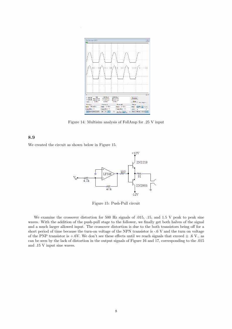
Figure 14: Multisim analysis of FollAmp for .25 V input
8.9
We created the circuit as shown below in Figure 15.
Figure 15: Push-Pull circuit
We examine the crossover distortion for 500 Hz signals of .015, .15, and 1.5 V peak to peak sinewaves. With the addition of the push-pull stage to the follower, we finally get both halves of the signaland a much larger allowed input. The crossover distortion is due to the both transistors being off for ashort period of time because the turn-on voltage of the NPN transistor is -.6 V and the turn on voltageof the PNP transistor is +.6V. We don’t see these effects until we reach signals that exceed ± .6 V., ascan be seen by the lack of distortion in the output signals of Figure 16 and 17, corresponding to the .015and .15 V input sine waves.
8
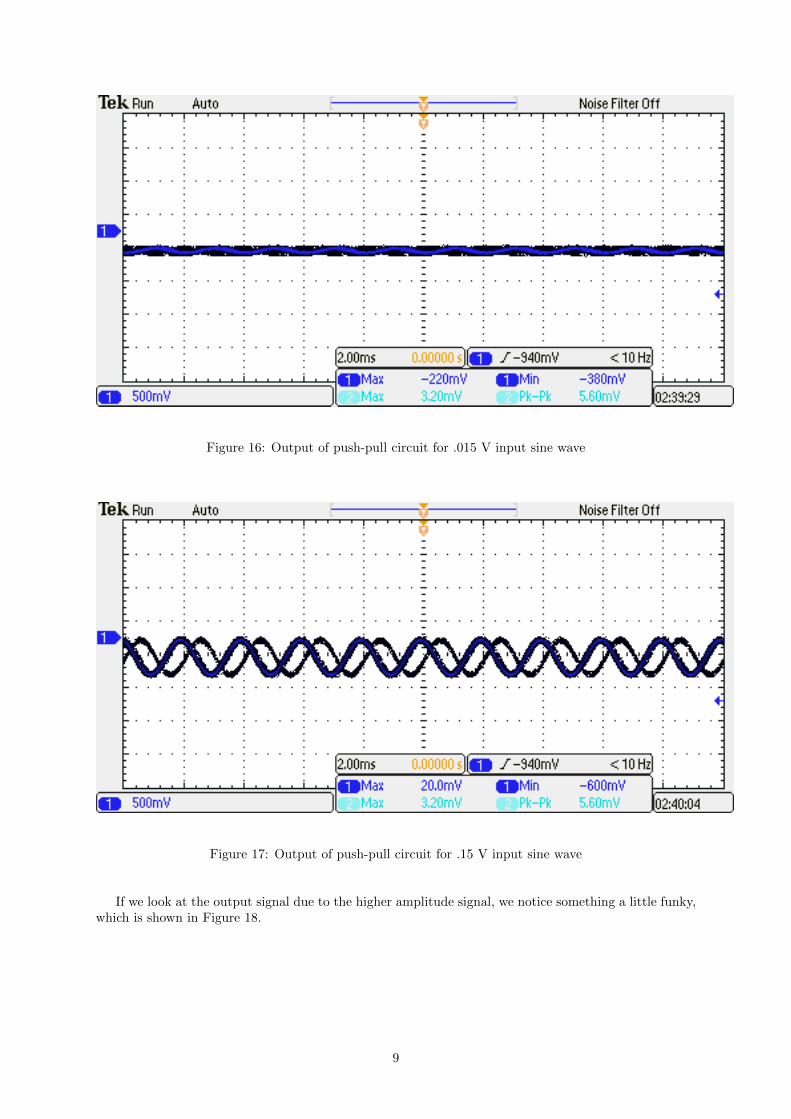
Figure 16: Output of push-pull circuit for .015 V input sine wave
Figure 17: Output of push-pull circuit for .15 V input sine wave
If we look at the output signal due to the higher amplitude signal, we notice something a little funky,which is shown in Figure 18.
9
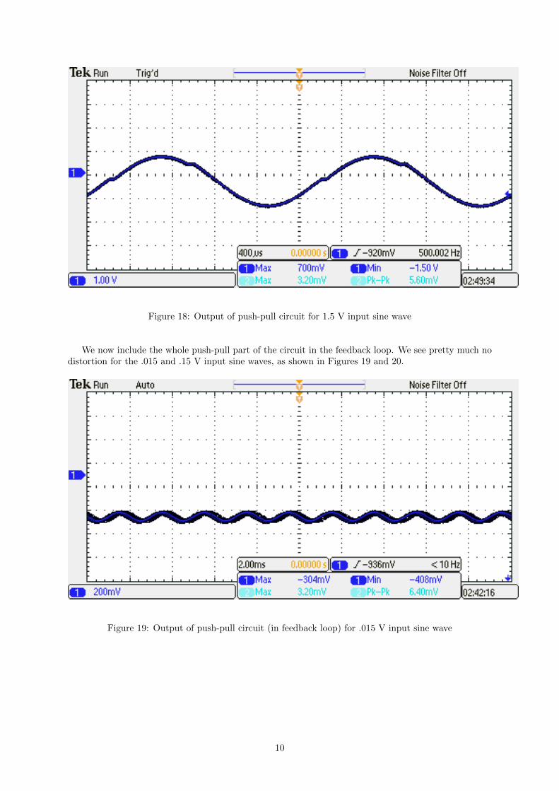
Figure 18: Output of push-pull circuit for 1.5 V input sine wave
We now include the whole push-pull part of the circuit in the feedback loop. We see pretty much nodistortion for the .015 and .15 V input sine waves, as shown in Figures 19 and 20.
Figure 19: Output of push-pull circuit (in feedback loop) for .015 V input sine wave
10
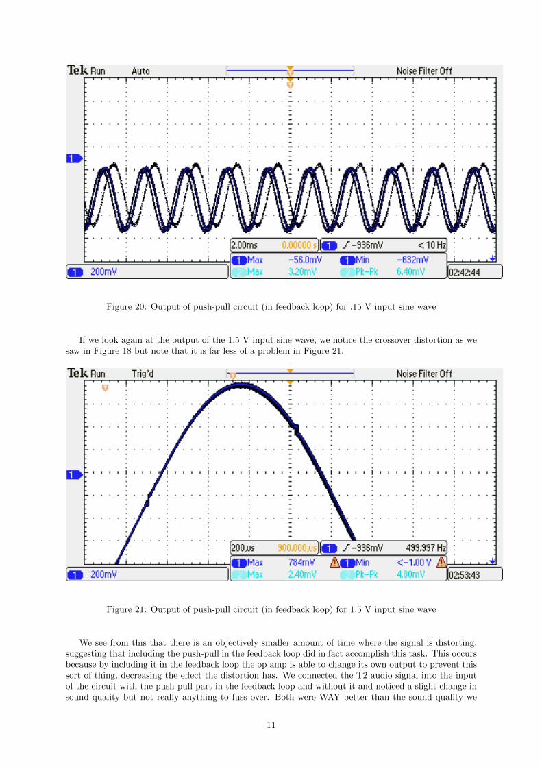
Figure 20: Output of push-pull circuit (in feedback loop) for .15 V input sine wave
If we look again at the output of the 1.5 V input sine wave, we notice the crossover distortion as wesaw in Figure 18 but note that it is far less of a problem in Figure 21.
Figure 21: Output of push-pull circuit (in feedback loop) for 1.5 V input sine wave
We see from this that there is an objectively smaller amount of time where the signal is distorting,suggesting that including the push-pull in the feedback loop did in fact accomplish this task. This occursbecause by including it in the feedback loop the op amp is able to change its own output to prevent thissort of thing, decreasing the effect the distortion has. We connected the T2 audio signal into the inputof the circuit with the push-pull part in the feedback loop and without it and noticed a slight change insound quality but not really anything to fuss over. Both were WAY better than the sound quality we
11

heard in 8.5 and 8.6
8.10
We obtained the strange commercial preamp and attached it into the circuit we built in Figure 21.
Figure 22: Output of push-pull circuit (in feedback loop) for .15 V input sine wave
We set the preamp gain to 100 and set its low pass filter to 100kHz and its high pass filter to 1kHz.We then measured the RMS noise from the op amp by setting R=0 and we found it to be 2.2 mV. Wethen looked at the signal on the scope and found its peak to peak to be 9.4 mV. Divided by six, that’s1.6 mV for the RMS, which is a pretty good estimation considering how crude the measurement is inthe first place. We then replaced the R=0 with a 1 MΩ resistor and found the RMS value to be 32 mV.We then looked at the scope and noticed that the peak to peak value of the noise was about 160 mV.If we divide this by six, we get about 27 mV which is also a pretty good estimate for the RMS value,suggesting the approximation is a decent one, albeit far from accurate. We have to divide both all of ourestimations by 100 as we used the preamp to amplify the signal by a gain of 100 so we actually foundnoise levels of 94 µ V and 320µV respectively.
8.11
We used the LabView Noise Generator program to create several different data sets of Gaussian dis-tributed white noise. The histograms for the amplitudes of this data are Gaussian distributed as wellas the spectra, because the inverse Fourier transform of a Gaussian will always just be a Gaussian. Thenoise has a uniform distribution of amplitude, rather than a Gaussian one, but they sound pretty muchthe same when played over the speakers. We also played the 1/f white noise through the speakers. Forthese, the overall average amplitude falls off as 1/f. This sounded like the Gaussian noise but with aslightly lower pitch. Gaussian noise that was cut off sounded a lot more like a really old air conditionerbecause there are almost no higher pitched overtones on top of the lower noise. Though the amplitudesof the overtones are very small for the 1/f noise, they are sadly present. The shot noise data with low Nsounds like wind rustling leaves. If you increase the average shots per sample the data set begins to soundnoisier as individual shots become indistinguishable. The amplitude histogram eventually approachesa Gaussian distribution, which makes sense since the limit as N approaches large of Poisson noise isGaussian. Because the data is normalized, the overall volume decreases if any particular frequency’samplitude is lowered. Thus, we can obtain a wider range of frequencies, but at decreased amplitudes.The line noise sounds terrible but I have heard this sound from the background noise of electronics likemy computer.
8.12
We ran the Multisim schematic ”DirectGn” and the bode plot is shown below in Figure 23 which showsthe gain and phase shift of the signal as a function of the frequency.
12
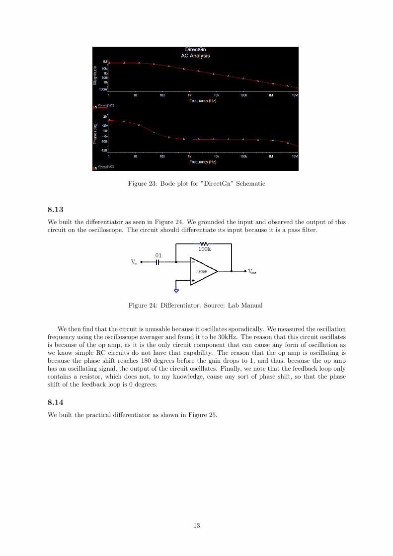
Figure 23: Bode plot for ”DirectGn” Schematic
8.13
We built the differentiator as seen in Figure 24. We grounded the input and observed the output of thiscircuit on the oscilloscope. The circuit should differentiate its input because it is a pass filter.
Figure 24: Differentiator. Source: Lab Manual
We then find that the circuit is unusable because it oscillates sporadically. We measured the oscillationfrequency using the oscilloscope averager and found it to be 30kHz. The reason that this circuit oscillatesis because of the op amp, as it is the only circuit component that can cause any form of oscillation aswe know simple RC circuits do not have that capability. The reason that the op amp is oscillating isbecause the phase shift reaches 180 degrees before the gain drops to 1, and thus, because the op amphas an oscillating signal, the output of the circuit oscillates. Finally, we note that the feedback loop onlycontains a resistor, which does not, to my knowledge, cause any sort of phase shift, so that the phaseshift of the feedback loop is 0 degrees.
8.14
We built the practical differentiator as shown in Figure 25.
13
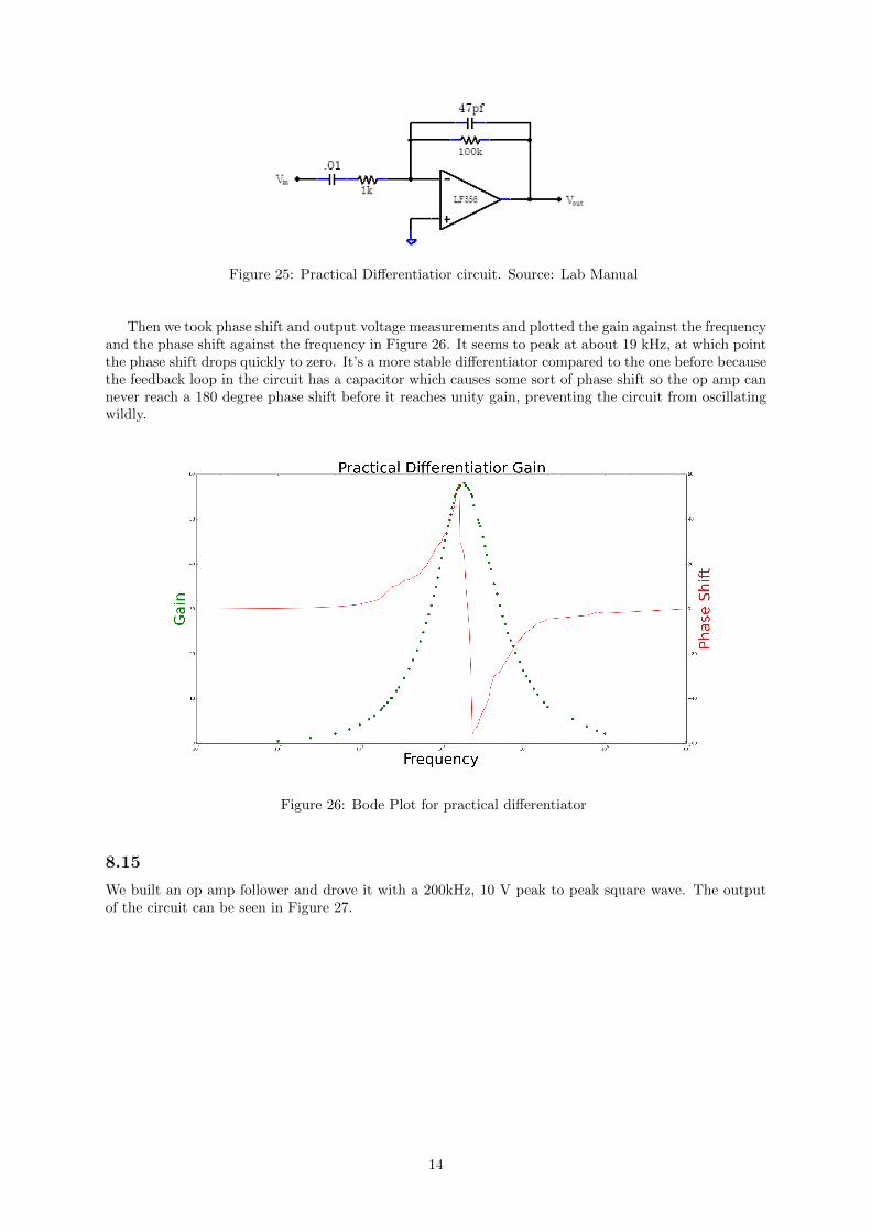
Figure 25: Practical Differentiatior circuit. Source: Lab Manual
Then we took phase shift and output voltage measurements and plotted the gain against the frequencyand the phase shift against the frequency in Figure 26. It seems to peak at about 19 kHz, at which pointthe phase shift drops quickly to zero. It’s a more stable differentiator compared to the one before becausethe feedback loop in the circuit has a capacitor which causes some sort of phase shift so the op amp cannever reach a 180 degree phase shift before it reaches unity gain, preventing the circuit from oscillatingwildly.
Figure 26: Bode Plot for practical differentiator
8.15
We built an op amp follower and drove it with a 200kHz, 10 V peak to peak square wave. The outputof the circuit can be seen in Figure 27.
14
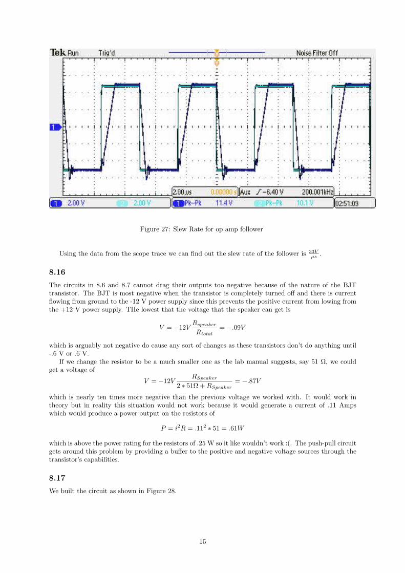
Figure 27: Slew Rate for op amp follower
Using the data from the scope trace we can find out the slew rate of the follower is 33Vµs .
8.16
The circuits in 8.6 and 8.7 cannot drag their outputs too negative because of the nature of the BJTtransistor. The BJT is most negative when the transistor is completely turned off and there is currentflowing from ground to the -12 V power supply since this prevents the positive current from lowing fromthe +12 V power supply. THe lowest that the voltage that the speaker can get is
V = −12VRspeakerRtotal
= −.09V
which is arguably not negative do cause any sort of changes as these transistors don’t do anything until-.6 V or .6 V.
If we change the resistor to be a much smaller one as the lab manual suggests, say 51 Ω, we couldget a voltage of
V = −12VRSpeaker
2 ∗ 51Ω +RSpeaker= −.87V
which is nearly ten times more negative than the previous voltage we worked with. It would work intheory but in reality this situation would not work because it would generate a current of .11 Ampswhich would produce a power output on the resistors of
P = i2R = .112 ∗ 51 = .61W
which is above the power rating for the resistors of .25 W so it like wouldn’t work :(. The push-pull circuitgets around this problem by providing a buffer to the positive and negative voltage sources through thetransistor’s capabilities.
8.17
We built the circuit as shown in Figure 28.
15
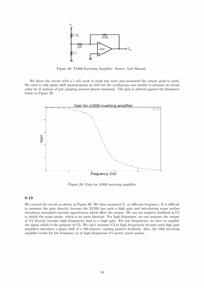
Figure 28: X1000 Inverting Amplifier. Source: Lab Manual,
We drove the circuit with a 1 mV peak to peak sine wave and measured the output peak to peak.We tried to take phase shift measurements as well but the oscilloscope was unable to measure an actualvalue for it instead of just jumping around almost randomly. The gain is plotted against the frequencybelow in Figure 29.
Figure 29: Gain for x1000 inverting amplifier
8.18
We created the circuit as shown in Figure 30. We then measured V- at different frequency. It is difficultto measure the gain directly because the LF356 has such a high gain and introducing scope probesintroduces unwanted external capacitances which effect the output. We can use negative feedback in U2to shield the scope probe, which is its main function. For high frequenies, we can measure the outputof U2 directly because high frequencies lead to a high gain. For low frequencies, we have to amplifythe signal which is the purpose of U3. We can’t measure U3 at high frequencies because such high gainamplifiers introduce a phase shift of a 180 degrees, causing positive feedback. Also, the 100x invertingamplifier works for low frequency so at high frequencies it’s pretty much useless.
16
Frequency (Hz) Vout (mV) V- (mV) Phase Shift Gain100 500 26 176 19.231 k 500 30 123 16.310 k 520 120 91 4.33100 k 560 400 -155.5 1.41 M 520 96 76 5.41
Figure 30: High DC gain circuit. Source: Lab Manual
8.19
We are attempting to calculate the gain of an inverting amplifier. We first note that
V+ − V− =VoutGopen
We have V+ grounded so we write
V− ·Gopen = Vout
V− is essentially grounded if we assume that Gopen is arbitrarily large.
Vin = V− − I ·R1
Vout = V− + I ·R2
We solve some algebra to get rid of the current and find that
R2
R1Vin =
R1 +R2
R1V− − Vout
Then we substitute for V−
Vin = VoutR1 +R2 −R1G
R2G
G =VoutVin
=R2
R1+R2
G −R1
When using the values we had, it does not appear to math the gains we measured. It seem that we mayhave made some sort of measurement error or we may have simply taken the data at the wrong pointsand gotten U2 and U3 mixed up. This is rather unfortunate.
8.20
We built the simple active rectifier as shown in Figure 31. We drove it with a triangle wave and observedits output at 1 kHz. The circuit properly rectified the signal there but when we looked at higherfrequencies it began to turn funky. It works at low frequencies because the output signal of the op ampwill be whatever voltage needs to pass through the diode to make V− equal to V+ and thus Vout equalto Vin. This is only possible when the diode is forward biased so when Vin is negative, the output of theo amp will go as negative a it can t omake V− negative because an increase in the output of the op amp
17
will make V− more positive and further away from Vin. Since the diode is in the circuit in reverse, ifthe op amp output is negative, Vout will be zero, rectifying the signal. Whenever Vin goes from negativeto positive, the output of the op amp shifts from -12V to some smaller positive value which is okay forlower frequency inputs
Figure 31: Active Rectifier circuit. Source: Lab Manual
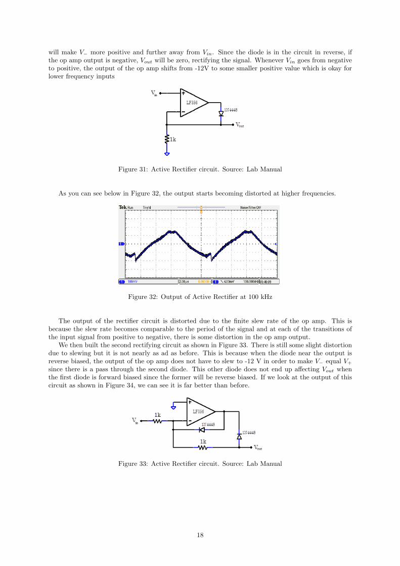
As you can see below in Figure 32, the output starts becoming distorted at higher frequencies.
Figure 32: Output of Active Rectifier at 100 kHz
The output of the rectifier circuit is distorted due to the finite slew rate of the op amp. This isbecause the slew rate becomes comparable to the period of the signal and at each of the transitions ofthe input signal from positive to negative, there is some distortion in the op amp output.
We then built the second rectifying circuit as shown in Figure 33. There is still some slight distortiondue to slewing but it is not nearly as ad as before. This is because when the diode near the output isreverse biased, the output of the op amp does not have to slew to -12 V in order to make V− equal V+since there is a pass through the second diode. This other diode does not end up affecting Vout whenthe first diode is forward biased since the former will be reverse biased. If we look at the output of thiscircuit as shown in Figure 34, we can see it is far better than before.
Figure 33: Active Rectifier circuit. Source: Lab Manual
18
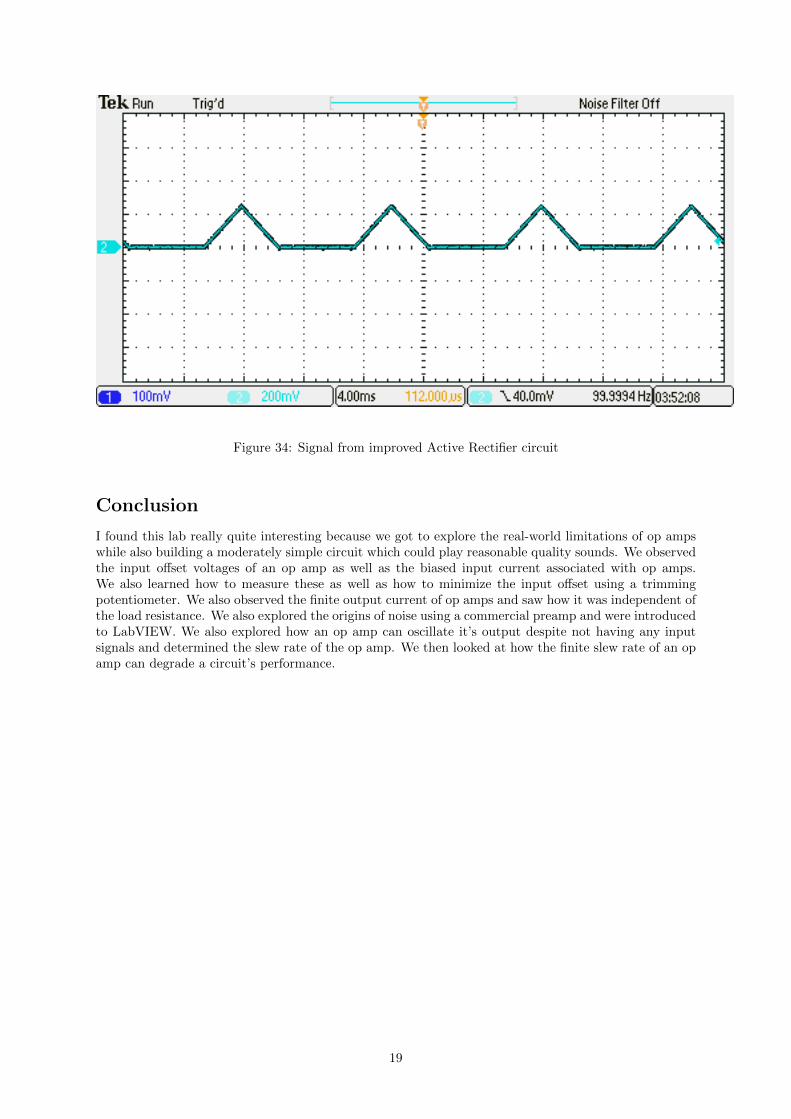
Figure 34: Signal from improved Active Rectifier circuit
Conclusion
I found this lab really quite interesting because we got to explore the real-world limitations of op ampswhile also building a moderately simple circuit which could play reasonable quality sounds. We observedthe input offset voltages of an op amp as well as the biased input current associated with op amps.We also learned how to measure these as well as how to minimize the input offset using a trimmingpotentiometer. We also observed the finite output current of op amps and saw how it was independent ofthe load resistance. We also explored the origins of noise using a commercial preamp and were introducedto LabVIEW. We also explored how an op amp can oscillate it’s output despite not having any inputsignals and determined the slew rate of the op amp. We then looked at how the finite slew rate of an opamp can degrade a circuit’s performance.
19